

Page 1
For Audio Equipment
MN6460A
A/D Converter for Digital Audio Equipment
Overview
The MN6460A is a 16-bit CMOS analog-to-digital
converter designed especially for PCM digital audio
equipment. It features a built-in digital filter. It uses noise
shaping to convert an analog signal to a 16-bit digital
signal.
Incorporating digital filter permits simplification of the
analog filter that normally precedes the A/D converter,
thus greatly reducing the power consumption of the
overall A/D conversion system.
Features
Analog and digital-mixed CMOS LSI
A/D conversion using noise shaping
64-fold oversampling
Built-in digital filter
Sample and hold circuit is unnecessary
Serial output using two's complement code
Built-in offset compensation circuit
Built-in overflow limiter
Single 5-volt power supply (when V
AG=2.5 V)
=1.5 V and
REF
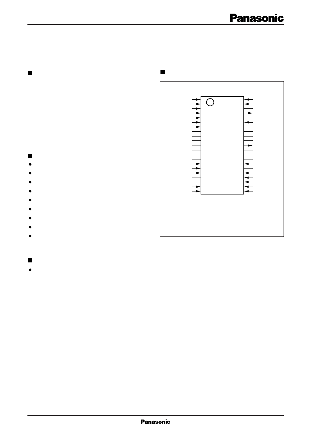
Pin Assignment
DV
DD
LR–POL
I–E
LR–CLK
B–CLK
CLR
OFCLR
N.C.
N.C.
N.C.
N.C.
N.C.
N.C.
N.C.
EXCLK
CV
CV
N.C.
N.C.
AV
AV
1
2
3
4
5
6
7
8
9
10
11
12
13
14
15
16
SS
17
DD
18
19
20
SS
21
DD
SSOP042-P-0450
(TOP VIEW)
DV
42
41
40
39
38
37
36
35
34
33
32
31
30
29
28
27
26
25
24
23
22
SS
TEST
N.C.
DOUT
N.C.
NSUB
N.C.
N.C.
N.C.
N.C.
TCLK
N.C.
N.C.
N.C.
AMPBIAS
N.C.
AV
SS
AV
DD
AIN
AG
V
REF
Applications
DAT players and other digital audio equipment
Page 2
MN6460A For Auido Equipment
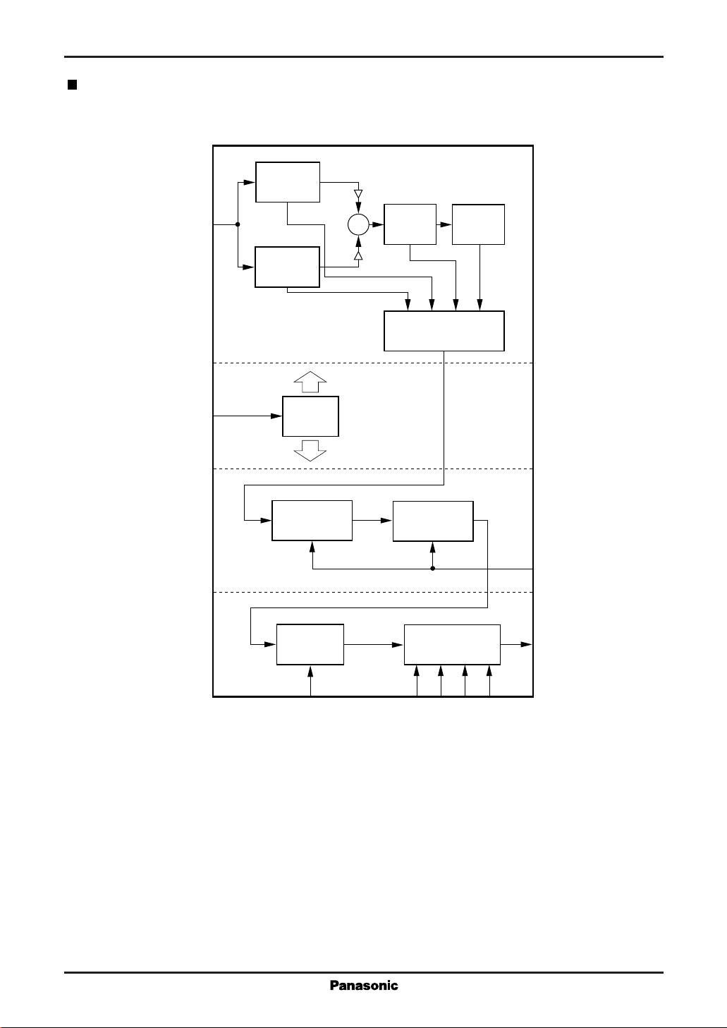
Block Diagram
DSQ:1bit Delta Sigma Quantizer
AIN
1st DSQ (+)
24
1st DSQ (–)
A/D converter
× 1/2
× 1/2
+
–
2nd DSQ
Summing logic
3rd DSQ
EXCLK
15
Digital filter
Clock
Generator
FIR 1
Comb-filter
OFFSET
Canceller
7
OFCLR
FIR 2
Low-pass-filter
P/S
Converter
2
3
I-E
LR-POL
4
LR-CLK
5
B-CLK
6
CLR
39
DOUT
Page 3

For Audio Equipment
Pin Descriptions
Pin No. Symbol Function Description
1DVDDPower supply pin for digital circuits (+5 V)
2 LR-POL Channel selection pin for stereo operation using two chips.
"H" level: right channel. "L" level: left channel.
3 I-E Format selection pin. "L" level: signal processing LSI format. "H" level: I2S format.
4 LR-CLK LRCLK input pin (for stereo operation)
If LR-POL is at "H" level, "H" level: right channel data output.
"L" level, high-impedance state.
If LR-POL is at "L" level, "H" level: high-impedance state.
"L" level, left channel data output.
5 B-CLK Bit transfer command input (At falling edge signal, a bit transfered)
6 CLR Clear pin. Active high.
Driving this pin at "H" level clears internal data. Always this internal
data is cleared by feeding a positive pulse to this pin after applying the power.
7 OFCLR Driving this pin at "L" level enables the offset clear circuit.
8 N.C. No connection (Leave this pin open.)
9 N.C. No connection (Leave this pin open.)
10 N.C. No connection (Leave this pin open.)
11 N.C. No connection (Leave this pin open.)
12 N.C. No connection (Leave this pin open.)
13 N.C. No connection (Leave this pin open.)
14 N.C. No connection (Leave this pin open.)
15 EXCLK 512 fs input pin
16 CV
17 CV
SS
DD
18 N.C. No connection (Leave this pin open.)
19 N.C. No connection (Leave this pin open.)
20 AV
21 AV
22 V
SS
DD
REF
23 AG Analog ground input pin (+2.5 V)
24 AIN Analog input pin
25 AV
26 AV
DD
SS
27 N.C. No connection (Leave this pin open.)
28 AMPBIAS Bias voltage adjustment pin for operational amplifier
29 N.C. No connection (Leave this pin open.)
30 N.C. No connection (Leave this pin open.)
31 N.C. No connection (Leave this pin open.)
Ground pin for digital circuits
Power supply pin for digital circuits (+5 V)
Ground pin for analog circuits
Power supply pin for analog circuits (+5 V)
Analog circuit reference voltage input pin (+1.5 V)
Power supply pin for analog circuits (+5 V)
Ground pin for analog circuits
(Keep this at the same voltage as the AG pin.)
MN6460A
Page 4

MN6460A For Auido Equipment
Pin Descriptions (continued)
Pin No. Symbol Function Description
32 TCLK LSI test clock output pin. (Leave this pin open.)
33 N.C. No connection (Leave this pin open.)
34 N.C. No connection (Leave this pin open.)
35 N.C. No connection (Leave this pin open.)
36 N.C. No connection (Leave this pin open.)
37 NSUB Connect this pin to AVDD.
38 N.C. No connection (Leave this pin open.)
39 DOUT Serial output pin. Two's complement. MSB first.
40 N.C. No connection (Leave this pin open.)
41 TEST LSI test pin. (Connect this pin to DVDD.)
42 DV
SS
Electrical Characteristics
Conversion Characteristics
DVDD=5.0V, AVDD=5.0V, VAG=2.5V, V
Parameter Symbol Test Condition min typ max Unit
Signal-to-noise ratio S/N EIAJ (1kHz) 85 90 dB
Ground pin for digital circuits
REF
=1.5V, f
=24.576MHz, Ta=25˚C
EXCLK
Dynamic range D.R. EIAJ (1KHZ) 85 90 dB
Total harmonic
THD+N EIAJ (1kHz) 0.005 0.010 %
distortion
Specifications for DC Offset
An A/D converter usually does not produce digital zero output from analog zero input because the operational
amplifier inside has an offset. The MN6460A, however, has circuitry for correcting this. The shipping inspection
enables this offset correction circuit and confirms that the DC offset is within the lower four bits.
Parameter Symbol Test Condition min typ max Unit
DC offset
OFCLR="H" ±20 mV
OFCLR="L" ±0.6 mV
Page 5

For Audio Equipment
Application Circuit Example
R1
D1
10kΩ
1
R7
10kΩ
14 13 12 11 10 9 8
1
23456 7
C5
0.1µF
141516 13 12 11 10 9
HC123
10µF
+
C8
SW1
HC32
+
C3
4.7µF
LR-CLK
B-CLK
CLR
OFCLR
GND 5V
D.GND
DD
D.V
–
+
100µF
–
+
100µF
CLR
4.7µF
+
C1
4.7µF
+
C15 C16
+
C2
+
4.7µF 4.7µF
8234567
4.7µF
+
C7
EXCLK-L
4.7µF
C15
4.7µF
C16
10µF
+
+
+
1
1
C12
141516 13 12 11 10 9
HC161.counter
141516 13 12 11 10 9
HC161.counter
MN6460A
256Fs
LRCK
DATA
BCK
14 13 12 1110 9 8
4.7µF
+
C22
8234567
8234567
1
14 13 12 11 10 9 8
+
C23
4.7µF
1
14 13 12 11 10 9 8
1
23456 7
HC74.D-FF
234567
XTAL.512Fs
234567
330Ω
HC32
+
C24
4.7µF
SW
10µF
256Fs
R18
+
512Fs
EXCLK-R
4.7kΩ
C33
20 19 18 17 141516 13 12
4.7µF
C44
+
1
2
R16
HC244
3456 7
11
1098
A.GND
DD
A.V
–12V
A.GND
12V
–
+
100µF
DV
1
1
DD
LR-POL
2
I-E
3
LR-CLK
4
B-CLK
5
CLR
6
OFCLR
7
N.C.
8
N.C.
9
N.C.
10
N.C.(TP0)
11
N.C.(TP1)
12
EXCLK-L
N.C.(TP2)
13
N.C.(TP3)
14
EXCLK
15
10µF
CV
16
C3
SS
+
CV
17
DD
N.C.
18
4.7µF
+
N.C.
19
C41
–
AV
20
+
C16C15 C15 C16
C5
+
4.7µF 4.7µF
100µF
SS
+
AV
21 22
C5
DD
DV
TEST
N.C.
DOUT
N.C.
NSUB
N.C.
N.C.
N.C.
N.C.
TCLK
N.C.
MN6460A
N.C.
N.C.
AMPBIAS
N.C.
AV
AV
AIN
V
42DV
SS
41
40
39
C41
+
38
4.7µF
37
36
35
34
33
32
31
30
R11
VR3
10kΩ
10kΩ
29
28
27
26
SS
25
DD
1000pF
24
AG
23
REF
4.7µF
C18
C23
C41
+
R4
1kΩ
R8
22kΩ
10kΩ
10kΩ
100pF
R3
100µF
+
C17
0.1µF
4.7kΩ
R7
10kΩ
C13
++
C13
3.3µF
1kΩ
VR1
R5
C19
5
6
7
8
1
2
3
4
5
6
HAF0614.LPF
7
0.1µF
C19
–
VR2
22µF
C11
+
22µF
R5
10kΩ
10kΩ
4
+
3
2
1
33µF
C29
C28
+
100µF
C38
–
100µF
1.2kΩ
R9
4.7µF
C14
+
R12
10kΩ
Ain(L)
2
EXCLK-R
3
4
5
6
7
8
9
10
11
12
13
14
15
10µF
16
C26
++
17
18
4.7µF
19
C41
20
–
+
C5
21 22
100µF
R12
22µF
C27
33µF
C32
C31
–
–
+
1
100µF
2
3
C33
+
+
–
4
100µF
5
R22
R10
6
1.2kΩ
7
R21
1.2kΩ
1.2kΩ
Ain(R)
DV
DD
LR-POL
I-E
LR-CLK
B-CLK
CLR
OFCLR
N.C.
N.C.
N.C.
N.C.(TP0)
N.C.(TP1)
N.C.(TP2)
N.C.(TP3)
EXCLK
CV
SS
CV
DD
N.C.
N.C.
AV
SS
AV
DD
HAF0614.LPF
TEST
N.C.
DOUT
N.C.
NSUB
N.C.
N.C.
N.C.
N.C.
TCLK
N.C.
MN6460A
N.C.
N.C.
AMPBIAS
N.C.
AV
AV
AIN
V
42
SS
41
40
39
C41
+
38
4.7µF
37
36
35
34
33
32
31
30
29
28
27
26
SS
25
DD
24
AG
23
REF
1000pF
+
4.7µF
C41
R23
10k
4.7µF
C37
R15
10kΩ
VR5
Ω
C43
0.1µF
C41
100µF
C42
+
–
+
C13
0.1µF
VR5
10kΩ
R28
4.7kΩ
R13
22kΩ
C30
++
3.3µF
10kΩ
1kΩ
R14
10kΩ
22µF
C13
C34
+
22µF
1kΩ
R17
VR4
R14
10kΩ
C36
100pF
Page 6

MN6460A For Auido Equipment
Package Dimensions (Unit: mm)
SSOP042-P-0450
21.25±0.20
2242
1.0±0.2
9.5±0.22.0±0.2
0.05
-
+0.10
0.15
0 to 10°
121
0.3min.
2.4max. 11.5±0.3
(0.6) 0.35±0.10
1.0
0.1±0.1
SEATING PLANE
 Loading...