

Page 1
MCM101525
1
MOTOROLA FAST SRAM
Product Preview
2M x 2 Bit Fast Static
Random Access Memory with
ECL I/O
The MCM101525 is a 4,194,304 bit static random access memory organized
as 2,097,152 words of 2 bits. This device features complementary outputs. This
circuit is fabricated using high performance silicon–gate BiCMOS technology.
Asynchronous design eliminates the need for external clocks or timing strobes.
The MCM101525 is available in a 400 mil, 36 lead TAB.
• Fast Access Times: 12, 15 ns
• Equal Address and Chip Select Access Time
• Power Operation: – 195 mA Maximum, Active AC
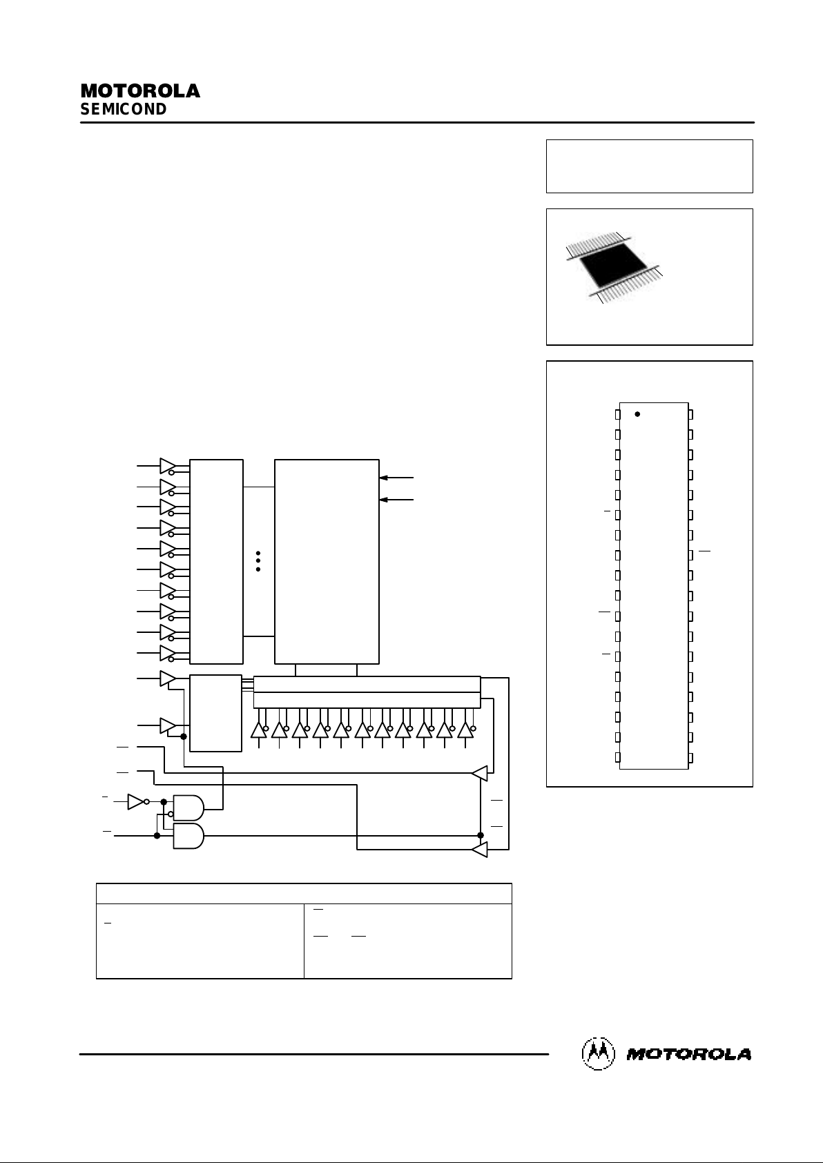
BLOCK DIAGRAM
ROW
DECODER
MEMORY MATRIX
1024 ROWS x
4096 COLUMNS
INPUT
DATA
CONTROL
COLUMN I/O
COLUMN DECODER
A15
A14
A13
A12
A11
A10
A9
A8
A18 A5 A3 A1
S
W
A16
A7 A6 A4 A2
Q0
Q0
Q1
Q1
A17
A0
D1
Q0
Q0
Q1
Q1
V
CC
V
EE
A20 A19
D0
A0 – A20 Address Inputs W Write Enable. . . . . . . . . . . . . . . . . . . . . . . . . . . . . . . . . .
S
Chip Select D0 – D1 Data Input. . . . . . . . . . . . . . . . . . . . . . . . . . . . . . . . . . . . . . . . .
Q0 – Q1 Data Output Q0
and Q1 Complementary Data Out. . . . . . . . . . . . . . . . . .
NC No Connection V
EE
Power Supply. . . . . . . . . . . . . . . . . . . . . . . . . . . . . . . . . . . .
V
CC
Ground. . . . . . . . . . . . . . . . . . . . . . . .
PIN NAMES
This document contains information on a new product under development. Motorola reserves the right to change or discontinue this product without notice.
Order this document
by MCM101525/D
MOTOROLA
SEMICONDUCTOR TECHNICAL DATA
PIN ASSIGNMENT
MCM101525
5
4
3
2
1
10
9
8
7
6
11
12
13
14
15
16
17
18
20
21
22
23
24
25
26
19
27
28
32
31
30
29
36
35
34
33
A13
A12
A11
A10
S
A14
V
EE
V
CC
Q0
D0
Q0
A15
A0
W
A17
A16
A18
V
CC
Q1
D1
NC
A9
A4
A5
A6
A7
V
EE
A3
A8
A19
NC
A20
Q1
A1
A2
TB PACKAGE
400 MIL TAB
CASE 984A–01
V
EE
Motorola, Inc. 1994
8/94
Page 2
MCM101525
2
MOTOROLA FAST SRAM
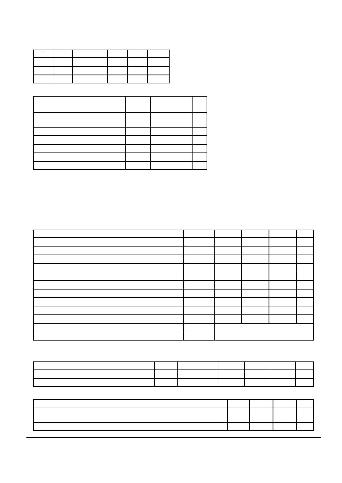
TRUTH TABLE (X = Don’t Care)
S
W Operation Data Output Current
H X Not Enabled X L —
L H Read X Q/Q I
EE
L L Write X L I
EE
ABSOLUTE MAXIMUM RATINGS (See Note)
Rating
Symbol Value Unit
VEE Pin Potential (to Ground) V
EE
– 7.0 to + 0.5 V
Voltage Relative to VCC for Any Pin
Except V
EE
Vin, V
outVEE
– 0.5 to+ 0.5 V
Output Current (per I/O) I
out
– 50 mA
Power Dissipation P
D
2.0 W
Temperature Under Bias T
bias
– 30 to + 85 °C
Operating Temperature T
J
0 to + 60 °C
Storage Temperature — Plastic T
stg
– 55 to + 125 °C
NOTE:Permanent device damage may occur if ABSOLUTE MAXIMUM RATINGS are
exceeded. Functional operation should be restricted to the OPERATING CONDITIONS. Exposure to higher than recommended voltages for extended periods of time
could affect device reliability.
DC OPERATING CONDITIONS AND CHARACTERISTICS
(VCC = 0 V, VEE = – 5.2 V ± 5%, TJ = 0 to + 60°C, Unless Otherwise Noted)
DC OPERATING CONDITIONS AND SUPPLY CURRENTS
Parameter Symbol Min Typ Max Unit
Supply Voltage (Operating Voltage Range) V
EE
– 5.46 – 5.2 – 4.94 V
Input High Voltage V
IH
– 1165 — – 880 mV
Input Low Voltage V
IL
– 1810 — – 1475 mV
Output High Voltage V
OH
– 1025 — – 880 mV
Output Low Voltage V
OL
– 1810 — – 1620 mV
Input Low Current I
IL
– 50 — — µA
Input High Current I
IH
— — 220 µA
Chip Select Input Low Current I
IL(CS)
0.5 — 170 µA
Operating Power Supply Current: tAVAV = 20 ns (All Outputs Open)* I
EE
— — – 195 mA
Quiescent Power Supply Current: fo = 0 MHz (Outputs Open) I
EEQ
— — – 150 mA
Voltage Compensation (VOH) ∆VOH/∆V
EE
± 35 mV/V @ – 4.94 to – 5.46 V
Voltage Compensation (VOL) ∆VOL/∆V
EE
± 60 mV/V @ – 4.94 to – 5.46 V
*Address Increment
RISE/FALL TIME CHARACTERISTICS
Parameter Symbol Test Condition Min Typ Max Unit
Output Rise Time t
r
20% to 80% 0.5 1.0 1.5 ns
Output Fall Time t
f
20% to 80% 0.5 1.0 1.5 ns
CAPACITANCE (f = 1.0 MHz, T
A
= 25°C, Periodically Sampled Rather Than 100% Tested)
Parameter
Symbol Typ Max Unit
Input Capacitance Address and Data
S
, W
C
in
C
ck
3.5
4
7
7
pF
Output Capacitance Q, Q C
out
4 8 pF
This device contains circuitry to protect
the inputs against damage due to high static
voltages or electric fields; however, it is advised that normal precautions be taken to
avoid application of any voltage higher than
maximum rated voltages to these high
impedance circuits.
This BiCMOS memory circuit has been
designed to meet the dc and ac specifications shown in the tables, after thermal equilibrium has been established. The circuit is
in a test socket or mounted on a printed circuit board and transverse air flow of at least
500 linear feet per minute is maintained.
Page 3
MCM101525
3
MOTOROLA FAST SRAM
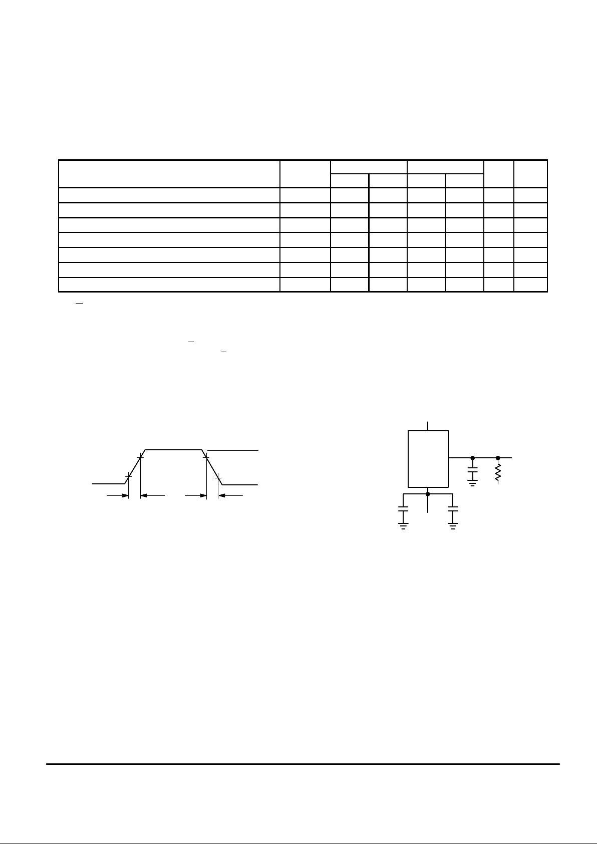
AC OPERATING CONDITIONS AND CHARACTERISTICS
(VEE = – 5.2 V ± 5%, VCC = 0 V, TJ = 0 to +60°C, Unless Otherwise Noted)
Input Pulse Levels – 1.7 V to – 0.9 V (See Figure 1). . . . . . . . . . . . .
Input Rise/Fall Time 1 ns. . . . . . . . . . . . . . . . . . . . . . . . . . . . . . . . . . . .
Input Timing Measurement Reference Level 50%. . . . . . . . . . . . . . . .
Output Timing Measurement Reference Level VOH = – 1165 mV. .
VOL = – 1475 mV
Output Load (AC Test Circuit) See Figure 2. . . . . . . . . . . . . . . . . . . . .
READ CYCLE TIMING (See Notes 1 and 2)
MCM101525–12 MCM101525–15
Parameter Symbol Min Max Min Max Unit Notes
Read Cycle Time t
AVAV
12 — 15 — ns 2, 3
Address Access Time t
AVQV
— 12 — 15 ns
Chip Select Access Time t
SLQV
— 12 — 15 ns 6
Select High to Output Low t
SHQL
0 8 0 9 ns
Output Hold from Address Change t
AXQX
4 — 4 — ns
Power Up Time t
SLIEEH
0 — 0 — ns 4
Power Down Time t
SHIEEL
— 12 — 15 ns 4
NOTES:
1. W
is high for read cycle.
2. Product sensitivites to noise require proper grounding and decoupling of power supplies during read and write cycles.
3. All read cycle timings are referenced from the last valid address to the first transitioning address.
4. This parameter is sampled and not 100% tested.
5. Device is continuously selected (S
≤ VIL).
6. Addresses valid prior to or coincident with S
going low.
80%
Figure 1. Input Levels Figure 2. AC Test Circuit
AC TEST CONDITIONS
50%
20% 20%
50%
80%
– 0.9 V
– 1.7 V
t
f
t
r
V
CC
V
EE
Q
C
L
R
L
– 2.0 V
0.01
µ
F0.1 µF
tr = Rise Time
tf = Fall Time
50% = Timing Reference Levels
RL = 50
Ω
CL = 30 pF
Page 4

MCM101525
4
MOTOROLA FAST SRAM
READ CYCLE 1 (See Notes 1, 2, and 5)
Q/Q (DATA OUT)
A (ADDRESS)
DATA VALIDPREVIOUS DATA VALID
t
AVAV
t
AXQX
t
AVQV
READ CYCLE 2 (See Note 6)
DATA VALID
t
SHQL
S (CHIP SELECT)
Q/Q
(DATA OUT)
t
SLQV
A (ADDRESS)
t
AVAV
t
SHIEEL
t
SLIEEH
SUPPLY CURRENT
IEE
Page 5

MCM101525
5
MOTOROLA FAST SRAM
WRITE CYCLE 1 (W Controlled, See Notes 1 and 2)
MCM101525–12 MCM101525–15
Parameter Symbol Min Max Min Max Unit Notes
Write Cycle Time t
AVAV
12 — 15 — ns 3
Address Setup Time t
AVWL
1 — 1 — ns
Address Valid to End of Write t
AVWH
9 — 10 — ns
Write Pulse Width t
WLWH
,
t
WLSH
8 — 9 — ns
Data Valid to End of Write t
DVWH
8 — 9 — ns
Data Hold Time t
WHDX
1 — 1 — ns
Write High to Output Active t
WHQX
4 — 4 — ns 4
Write High to Output Valid t
WHQV
— 13 — 16 ns
Write Recovery Time t
WHAX
1 — 1 — ns
Write Low to Output Low t
WLQL
0 8 0 9 ns
NOTES:
1. A write occurs during the overlap of S
low and W low.
2. Product sensitivites to noise require proper grounding and decoupling of power supplies during read and write cycles.
3. All write cycle timings are referenced from the last valid address to the first transitioning address.
4. This parameter is sampled and not 100% tested.
WRITE CYCLE 1 (W Controlled, See Notes 1, 2, and 3)
t
DVWH
t
AVWL
t
AVWH
t
AVAV
t
WHAX
t
WLWH
t
WHDX
t
WLQL
t
WHQX
A (ADDRESS)
S
(CHIP SELECT)
Q/Q
(DATA OUT)
D (DATA IN)
t
WLSH
W (WRITE ENABLE)
t
WHQV
DATA VALID
ADDRESS VALID
Motorola reserves the right to make changes without further notice to any products herein. Motorola makes no warranty , representation or guarantee regarding
the suitability of its products for any particular purpose, nor does Motorola assume any liability arising out of the application or use of any product or circuit,
and specifically disclaims any and all liability, including without limitation consequential or incidental damages. “T ypical” parameters can and do vary in different
applications. All operating parameters, including “T ypicals” must be validated for each customer application by customer’s technical experts. Motorola does
not convey any license under its patent rights nor the rights of others. Motorola products are not designed, intended, or authorized for use as components in
systems intended for surgical implant into the body, or other applications intended to support or sustain life, or for any other application in which the failure of
the Motorola product could create a situation where personal injury or death may occur. Should Buyer purchase or use Motorola products for any such
unintended or unauthorized application, Buyer shall indemnify and hold Motorola and its officers, employees, subsidiaries, affiliates, and distributors harmless
against all claims, costs, damages, and expenses, and reasonable attorney fees arising out of, directly or indirectly, any claim of personal injury or death
associated with such unintended or unauthorized use, even if such claim alleges that Motorola was negligent regarding the design or manufacture of the part.
Motorola and are registered trademarks of Motorola, Inc. Motorola, Inc. is an Equal Opportunity/Affirmative Action Employer.
Page 6

MCM101525
6
MOTOROLA FAST SRAM
WRITE CYCLE 2 (S Controlled, See Notes 1 and 2)
MCM101525–12 MCM101525–15
Parameter Symbol Min Max Min Max Unit Notes
Write Cycle Time t
AVAV
12 — 15 — ns 3
Address Setup Time t
AVSL
1 — 1 — ns
Address Valid to End of Write t
AVSH
9 — 10 — ns
Write Pulse Width (S)
(W
)
t
SLSH
t
SLWH
8 — 9 — ns
Data Valid to End of Write t
DVSH
8 — 9 — ns
Chip Select Set–Up Time t
SLWL
0 — 0 — ns
Data Hold Time t
SHDX
1 — 1 — ns
Write Recovery Time t
SHAX
1 — 1 — ns
NOTES:
1. A write occurs during the overlap of S
low and W low.
2. Product sensitivites to noise require proper grounding and decoupling of power supplies during read and write cycles.
3. All write cycle timings are referenced from the last valid address to the first transitioning address.
WRITE CYCLE 2 (S Controlled, See Notes 1 and 2)
t
SLWH
t
SHAX
t
DVSH
t
AVSL
t
SLSH
t
AVSH
DATA VALID
t
AVAV
A (ADDRESS)
W
(WRITE ENABLE)
S
(CHIP SELECT)
Q/Q
(DATA OUT)
D (DATA IN)
t
SHDX
t
SLWL
ORDERING INFORMATION
(Order by Full Part Number)
MCM 101525 XX XX XX
Motorola Memory Prefix
Part Number
Speed (12 = 12 ns, 15 = 15 ns)
Package (TB = TAB)
Shipping Method (Blank = Rails)
Full Part Numbers — MCM101525TB12
MCM101525TB15
Page 7

MCM101525
7
MOTOROLA FAST SRAM
TB PACKAGE
400 MIL TAB
CASE 984A–01
PACKAGE DIMENSIONS
19
VIEW AM
REF 3X
18
TAB
TAPE
WV
U
S1
S
R
TAB TAPE
CARRIER
K
J
AD
P
Z
SECTION AN–AN
DIMAMIN MAX MIN MAX
INCHES
18.14 REF 0.714 REF
MILLIMETERS
B 8.03 REF 0.316 REF
C 26.95 BSC 1.061 BSC
C1 26.95 BSC 1.061 BSC
J ––– 0.25 ––– 0.010
K ––– 0.71 ––– 0.028
P 3.00 REF 0.118 REF
R 2.39 REF 0.094 REF
S 50.00 REF 1.969 REF
S1 50.00 REF 1.969 REF
U 6.00 REF 0.236 REF
U1 6.00 REF 0.236 REF
V 39.40 REF 1.551 REF
W 45.68 REF 1.798 REF
Y 38.00 REF 1.496 REF
Z 1.15 1.25 0.045 0.049
AA 16.21 16.31 0.638 0.642
AB 11.20 11.30 0.441 0.445
AC 8.99 9.09 0.354 0.358
AD 0.15 0.21 0.006 0.008
AE 0.762 BSC 0.030 BSC
AF 0.18 0.28 0.007 0.011
AG 21.31 21.24 0.832 0.836
AH 35.00 REF 1.378 REF
AJ 25.40 REF 1.000 REF
AK 26.95 BSC 1.061 BSC
AL 34.98 REF 1.377 REF
AR 0.65 0.75 0.026 0.030
AS 0.50 BSC 0.020 BSC
AT 0.60 0.70 0.024 0.028
AU 26.95 REF 1.061 REF
AV 25.35 25.45 0.998 1.002
AV1 25.35 25.45 0.998 1.002
NOTES:
1. DIMENSIONING AND TOLERANCING PER
ANSI Y14.5M, 1982.
2. CONTROLLING DIMENSION: MILLIMETER.
U1
Y
RETAINER
CARRIER
1
36
B
VIEW AM
A
-M-
-H-
AN
AN
4X
1.40 (0.055)
H0.05 (0.002)ST M-N
S S
-N-
TAPE CARRIER RETAINER ELIMINATED
FROM VIEW FOR CLARITY
C1
C
-T-
Page 8

MCM101525
8
MOTOROLA FAST SRAM
TB PACKAGE
400 MIL TAB
CASE 984A–01 (cont.)
AV1
AV
BOTTOM VIEW
AU
REF 4X
2.00 (0.78)
AL
AE/2
AE
AK AJ
AA
AB
AC
H0.25 (0.010)ST M-N
S S
H0.25 (0.010)ST M-N
S S
VIEW AP
AH
36X AF
AG
H0.05 (0.0020) ST M-N
S S
4X
34X
AS
194X
196X
AR
H0.10 (0.004)LT M-N
S S
AT
REF AS
H0.10 (0.004)LT M-N
S S
VIEW AP
Literature Distribution Centers:
USA: Motorola Literature Distribution; P .O. Box 20912; Phoenix, Arizona 85036.
EUROPE: Motorola Ltd.; European Literature Centre; 88 T anners Drive, Blakelands, Milton Keynes, MK14 5BP, England.
JAPAN: Nippon Motorola Ltd.; 4–32–1, Nishi–Gotanda, Shinagawa–ku, Tokyo 141, Japan.
ASIA PACIFIC: Motorola Semiconductors H.K. Ltd.; Silicon Harbour Center, No. 2 Dai King Street, Tai Po Industrial Estate, Tai Po, N.T., Hong Kong.
MCM101525/D
*MCM101525/D*
◊
CODELINE TO BE PLACED HERE
 Loading...