

Page 1
Ordering number : EN5904
LA6543M
Monolithic Linear IC
LA6543M
4-Channel Bridge (BTL) Driver for CD-ROM
Overview
The LA6543M is a 4-channel bridge (BTL) driver
developed for CD-ROM applications.
Functions
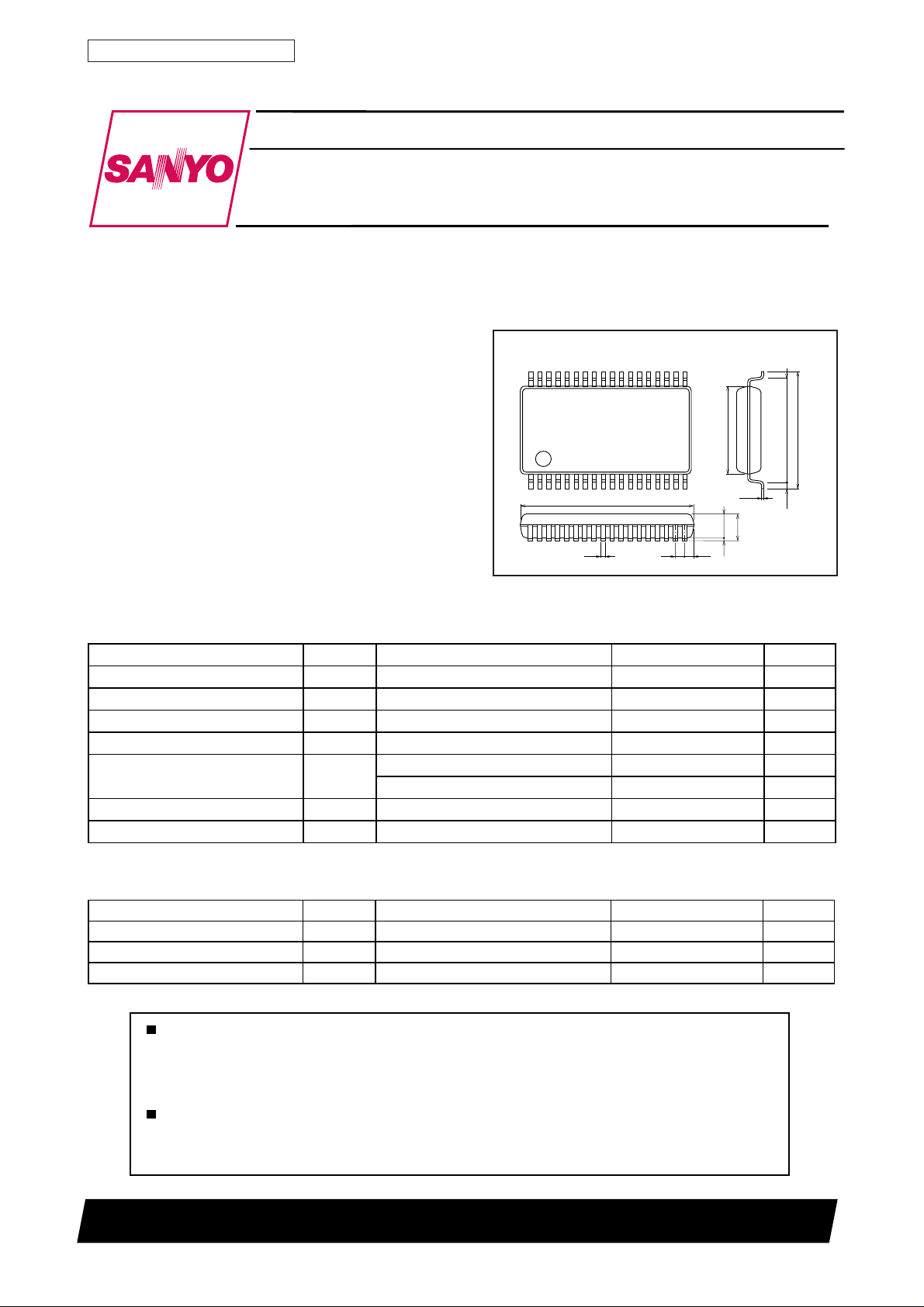
Package Dimensions
unit: mm
3129-MFP36SLF
[LA6543M]
36
19
• 4-channel power amplifier with bridge circuit (BTL)
• IO max: 1A
• Integrated muting circuit (MUTE: Output OFF at Low,
7.9
9.2
output ON at High. MUTE1 is for channel 1, and MUTE2
for channels 2, 3 and 4.)
• Integrated thermal shutdown circuit
• Divided output stage power supply (VS1: CH1, CH2, CH3;
VS2: CH4)
118
15.3
0.4
0.8
0.25
2.250.1
2.5max
0.85
SANYO : MFP36SLF
0.65
Specifications
Maximum Ratings at Ta = 25°C
Parameter Symbol Conditions Ratings Unit
Maximum supply voltage 1 14 V
Maximum supply voltage 2 14 V
Input voltage Input pins 13 V
Mute pin voltage 13 V
Allowable power dissipation Pd max IC only 0.9 W
Operating temperature Topr °C
Storage temperature Tstg °C
Note 1: Specified substrate 76.1 x 114.3 x 1.6 (t)mm, glass exposy
VCCmax
VSmax
VINmax
V
MUTE
VS1, 2
VIN1 to 4
max
Specified substrate Note 1 2.1 W
– 20 to +75
– 55 to +150
10.5
Operating Conditions at Ta = 25°C
Parameter Symbol Conditions Ratings Unit
Recommended operation voltage 1 4 to 13 V
Recommended operation voltage 2-1 4 to 13 V
Recommended operation voltage 2-2 4 to 13 V
*V
> VS1, 2
CC
Any and all SANYO products described or contained herein do not have specifications that can handle
applications that require extremely high levels of reliability, such as life-support systems, aircraft's
control systems, or other applications whose failure can be reasonably expected to result in serious
physical and/or material damage. Consult with your SANYO representative nearest you before using
any SANYO products described or contained herein in such applications.
SANYO assumes no responsibility for equipment failures that result from using products at values that
exceed, even momentarily, rated values (such as maximum ratings, operating condition ranges, or other
parameters) listed in products specifications of any and all SANYO products described or contained
herein.
V
CC
VS1
VS2
VS1: CH1 to CH3
VS2: CH4
output reference power supply
SANYO Electric Co., Ltd. Semiconductor Business Headquarters
TOKYO OFFICE Tokyo Bldg., 1-10, 1 Chome, Ueno, Taito-ku, TOKYO, 110-8534 JAPAN
N1798RM(KI)
No. 5904-1/7
Page 2
LA6543M
Electrical Characteristics at V
Parameter Symbol Conditions
VCC no-load current drain
1 no-load current drain
V
S
V
2 no-load current drain
S
Output offset voltage
Input voltage range 0.5 5 V
Output voltage (source) Vsource Plus and minus outputs at high level 4.4 4.7 V
(sink) Vsink Plus and minus outputs at low level 0.3 0.6 V
Closed circuit voltage gain VG1 Voltage gain between CH1 to CH3 BTL amplifiers 7 dB
Slew rate SR (Note 1) 0.5 V/µs
Mute ON voltage MUTE1, MUTE2 voltage when output is ON (Note 2) 1.5 2 V
Mute ON current MUTE1, MUTE2 current when output is ON (Note 2) 6 10 µA
= 12V, VS = 5V, Ta = 25°C
CC
Ratings
min typ max
All outputs ON (MUTE1, MUTE2: High) 5 10 20 mA
I
1
CC
I
2
All outputs OFF (MUTE1, MUTE2: Low) 5 10 mA
CC
1-1
I
CH1 - CH2 ON (MUTE1, MUTE2: High) 20 30 mA
S
CH1 - CH2 OFF (MUTE1, MUTE2: Low) 4 mA
1-2
I
S
CH3 - CH4 ON (MUTE1, MUTE2: High) 5 10 mA
2-1
I
S
CH3 - CH4 OFF (MUTE1, MUTE2: Low) 4 mA
2-2
I
S
VOF1 to 4
V
Potential difference between plus and minus outputs
for CH1 to CH4
Input voltage range for VIN1 to VIN4
V
IN
= 700 mA
I
O
I
= 700 mA
O
VG2 Voltage gain between CH4 BTL amplifiers 14 dB
MUTE
I
MUTE
–50 +50 mV
Unit
Note 1: Guaranteed design value
Note 2: MUTE turns amplifier output ON at High and OFF at Low. (Output impedance becomes high.) This applies to MUTE1 and
MUTE2.
2.4
With substrate
2.0
1.6
1.2
IC only
0.8
0.4
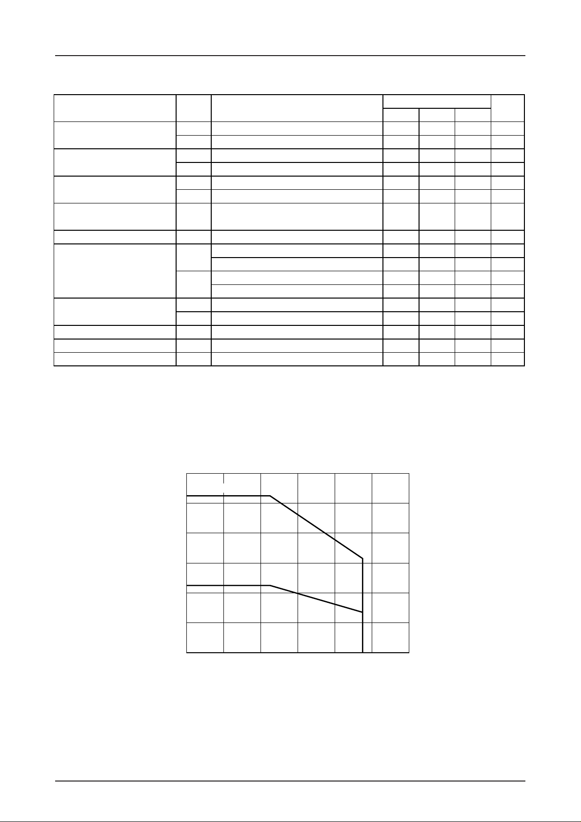
0
Allowable power dissipation, Pd max – mW
0–20 20 40 60 75 80 100
Pd max – Ta
2.1
0.9
Ambient temperature, Ta – ˚C
No. 5904-2/7
Page 3
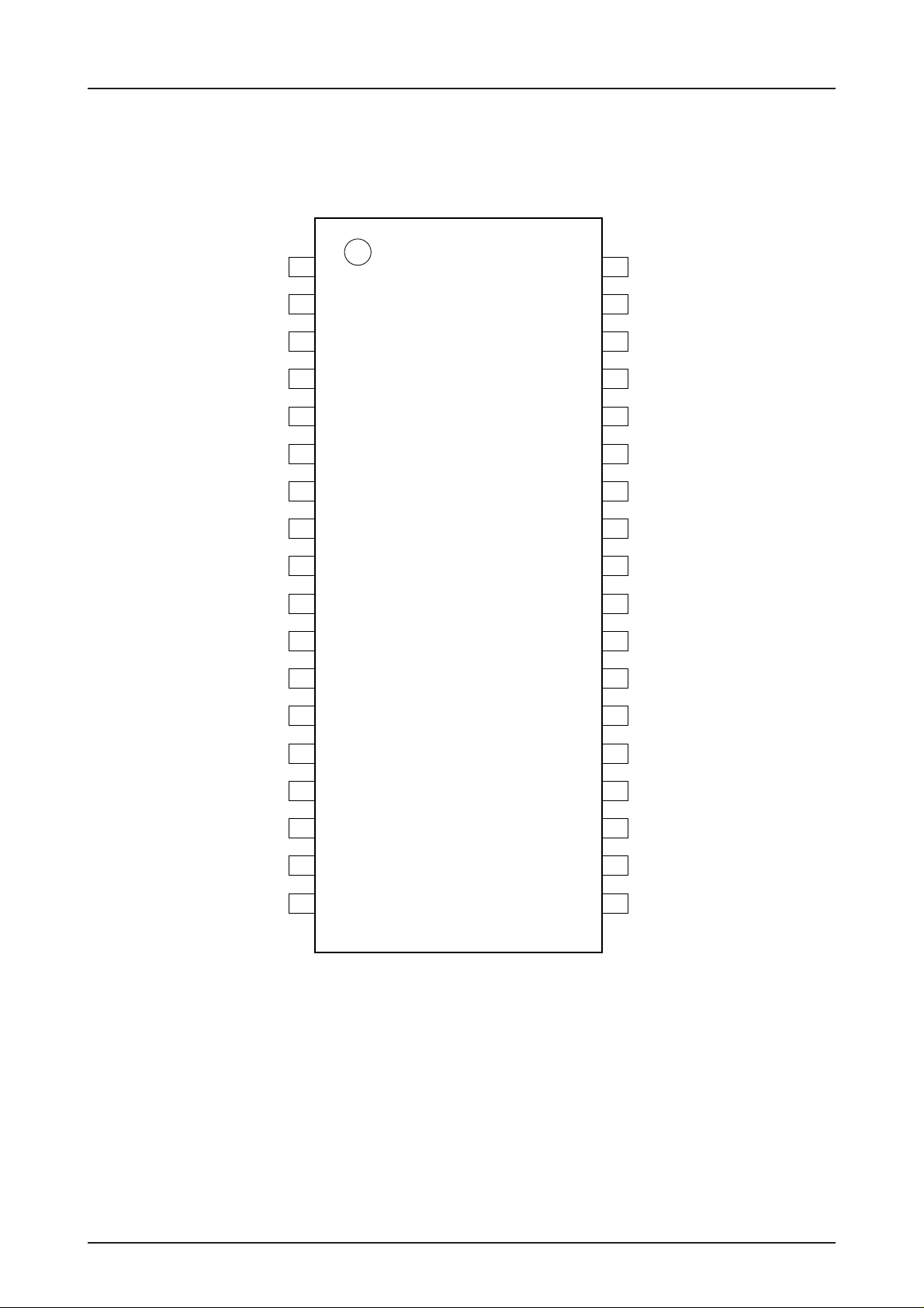
Pin Assignment
LA6543M
V
SS
RF
RF
NC
V
SS
2-OUT
MUTE1
V
IN
VG1
V
IN
VG2
V
IN
VG3
V
IN
1
2
3
4
2
5
6
7
1
8
9
2
36
35
34
33
32
31
30
29
28
RF
RF
V
V
V
V
V
V
V
SS
SS
O
O
S
O
O
1
2
1
3
4
1
1-OUT
LA6543M
10
11
3
12
13
4
27
26
25
24
5
V
O
6
V
O
V
2
S
7
V
O
VG4
MUTE2
V
CC
RF
RF
14
15
16
17
18
23
22
21
20
19
Top view
V
V
V
RF
RF
8
O
REF
REF
OUT
IN
A11323
No. 5904-3/7
Page 4

LA6543M
Pin Function
Pin number Pin name Equivalent circuit Pin function
1, 2
17, 18
19, 20
35, 36
7 Input pin for CH1
9 Input pin for CH2
11 Input pin for CH3
13 Input pin for CH4
8 VG1 Input pin for CH1 (gain adjustment)
10 VG2 Input pin for CH2 (gain adjustment)
12 VG3 Input pin for CH3 (gain adjustment)
14 VG4 Input pin for CH4 (gain adjustment)
16 Power supply
22 Level shift circuit reference voltage
3NC May not be used.
4 Connect to
5 Output stage reference voltage output
6 MUTE1 CH1 output ON/OFF
15 MUTE2 CH2 to CH4 output ON/OFF
R F Substrate (minimum potential)
V
CC
16
VIN1
V
2
IN
V
V
V
V
V
REF
VSS2
SS
3
IN
4
IN
CC
OUT
2-OUT
911
V
IN
713
11kΩ
812
VG
1014
16
A
V
CC
Drive
GND
1 2 17 18
V
OUT
REF
22
19 20 35 36
A10991
1 buffer amplifier output)
(V
REF
V
2
S
(V
2-VBE)/2: typ)
S
MUTE1,2
6
15
To bias circuit
1 2 17 18
19 20 35 36
A10993
IN
21 Level shift circuit reference voltage input
23 CH4 inverted output (AMP8 output)
24 CH4 non-inverted output (AMP7 output)
26 CH3 inverted output (AMP6 output)
27 CH3 non-inverted output (AMP5 output)
28 CH2 inverted output (AMP4 output)
29 CH2 non-inverted output (AMP3 output)
31 CH1 inverted output (AMP2 output)
32 CH1 non-inverted output (AMP1 output)
V
REF
V
V
V
V
V
V
V
V
8
O
7
O
6
O
5
O
4
O
3
O
2
O
1
O
23
V
O
24
29
2631
272832
Drive
V
CC
16
2 17
1 18
19 20 35 36
A10992
1 buffer amplifier input)
(V
REF
25 VS2 CH3 (AMP5, AMP6), CH4 (AMP7, AMP8)
output stage power supply
30 VS1 CH1 (AMP1, AMP2), CH2 (AMP3, AMP4)
output stage power supply
33 Output stage reference voltage
34 Connect to VS1 (resistance split to generate
VSS1-OUT
1
V
SS
(V
2 buffer amplifier input)
REF
1-OUT)
V
SS
(VSS1/2:typ)
No. 5904-4/7
Page 5

Block Diagram
LA6543M
1RF 36 RF
2RF 35 RF
3NC 34 VSS1
4VSS2 33 VSS1-OUT
5VSS2-OUT 32 VO1
VO1 to VO2
6MUTE1 31 VO2
Thermal shutdown
MUTE1 MUTE2
CH1(VO1-VO2)
–
+
CH2(VO3-VO4)
CH3(VO5-VO6)
CH4(VO7-VO8)
–
+
–
+
–
+
Level shift
7VIN1 30 VS1
8VG1 29 VO3
Level shift
9VIN2 28 VO4
10VG2 27 VO5
Level shift
11VIN3 26 VO6
–
+
–
+
–
+
–
+
12VG3 25 VS2
13VIN4 24 VO7
Level shift
14VG4 23 VO8
VO3 to VO8
15MUTE2 22 V
16V
CC
–
+
–
+
–
+
21 V
REF
REF
OUT
IN
17RF 20 RF
18RF 19 RF
System Diagram (relationship between power supply and MUTE)
MUTE1 CH1
CH2
MUTE2 CH3
CH4
VS1
VS2
A10995
A10994
No. 5904-5/7
Page 6

Sample Application Circuit
LA6543M
V
(5V)
S
Loading input
Focus input
Tracking input
Sled input
Gain setting
Gain setting
Gain setting
Gain setting
10
11
12
13
14
15
1
2
3
4
5
6
7
8
9
RF
RF
(NC)
V
2
SS
2-OUT
V
SS
MUTE1
1
V
IN
VG1
V
2
IN
VG2
3
V
IN
VG3
V
4
IN
VG4
MUTE2
LA6543M
V
V
SS
REF
RF
RF
V
SS
1-OUT
V
O
V
O
V
S
V
O
V
O
V
O
V
O
V
S
V
O
V
O
OUT
36
35
34
1
33
32
1
M
Loading
31
2
30
1
29
3
Focus
28
4
27
5
Tracking
26
6
25
2
24
7
Sled
M
23
8
22
VCC (12V)
16
17
18
V
RF
RF
CC
V
REF
IN
RF
RF
21
20
19
Reference
voltage
A10996
No. 5904-6/7
Page 7

LA6543M
Gain Setting (input pins and adjustment pins)
A simplified diagram of VIN and VG is shown below.
1) Consider an 11 kΩ (typ.) inserted between VIN and VG.
2) When only VIN and not VG is used, the BTL gain (between V
case when VIN is not used and an 11 kΩ external resistor is connected to VG for input.
3) Gain is set by the input impedance as seen from point A.
When VG only is used and the external resistor is R, the BTL gain (between V
20 log (11 kΩ/R) + 6 dB.
When an 11 kΩ resistor is inserted between VIN and VG, and input is via VIN, the combined resistance Rz as seen from point A is
Rz = 5.5 kΩ. Gain is
20 log (11 kΩ/5.5 kΩ) + 6 dB = 12 dB.
V
VG
V
REF
V
SS
IN
11 kΩ
–
V
REF
+
CH4 only
1
Level
A
O
shift
+
and V
–
) is set to 6 dB (0 dB for AMP only). This also applies for the
O
+
O
and V
O
–
) is
–
AMP1
+
–
AMP2
+
+
V
O
–
V
O
11 kΩ
11 kΩ
GND
–
V
2
REF
+
Offset Voltage
This IC incorporates a level shifter circuit. The input references the voltage V
voltage (VSS – VBE (0.7))/2V to be output.
Specifications of any and all SANYO products described or contained herein stipulate the performance,
characteristics, and functions of the described products in the independent state, and are not guarantees
of the performance, characteristics, and functions of the described products as mounted in the customer's
products or equipment. To verify symptoms and states that cannot be evaluated in an independent device,
the customer should always evaluate and test devices mounted in the customer's products or equipment.
SANYO Electric Co., Ltd. strives to supply high-quality high-reliability products. However, any and all
semiconductor products fail with some probability. It is possible that these probabilistic failures could
give rise to accidents or events that could endanger human lives, that could give rise to smoke or fire,
or that could cause damage to other property. When designing equipment, adopt safety measures so
that these kinds of accidents or events cannot occur. Such measures include but are not limited to protective
circuits and error prevention circuits for safe design, redundant design, and structural design.
In the event that any or all SANYO products(including technical data,services) described or
contained herein are controlled under any of applicable local export control laws and regulations,
such products must not be exported without obtaining the export license from the authorities
concerned in accordance with the above law.
No part of this publication may be reproduced or transmitted in any form or by any means, electronic or
mechanical, including photocopying and recording, or any information storage or retrieval system,
or otherwise, without the prior written permission of SANYO Electric Co. , Ltd.
Any and all information described or contained herein are subject to change without notice due to
product/technology improvement, etc. When designing equipment, refer to the "Delivery Specification"
for the SANYO product that you intend to use.
Information (including circuit diagrams and circuit parameters) herein is for example only ; it is not
guaranteed for volume production. SANYO believes information herein is accurate and reliable, but
no guarantees are made or implied regarding its use or any infringements of intellectual property rights
or other rights of third parties.
to be applied and references the
REF
A10997
This catalog provides information as of December, 1998. Specifications and information herein are subject to change
without notice.
PS
No. 5904-7/7
 Loading...