

Page 1
Ordering number: EN 5471
Monolithic Linear IC
LA7191N
Global VHS-format VCR
Video Signal Processor
Overview
The LA7191N is a multi-format, single-chip video signal
processing IC that supports TV systems around the world.
Features
.
Compatible with TV systems around the world (NTSC/
PAL/MESECAM/4.43 -NTSC/PAL-M/PAL-N).
.
All filters on chip, except for PB-LPF for chroma (cutoff
frequency requires no adjustment).
.
No adjustment of YNR and DOC levels.
.
Double high-pass noise canceller on chip.
.
Linear phase-type picture control on chip.
.
fsc output can be used as clock for OSD IC.
.
DCC circuit on chip.
.
Pilot burst erasure circuit on chip.
.
High-speed AFC circuit on chip.
.
Switching noise canceller on chip.
.
Smallest package in the industry.
.
Few components needed.
.
2fsc output.
.
I/O pin for CNR insertion added.
.
YNR/LNC switching possible.
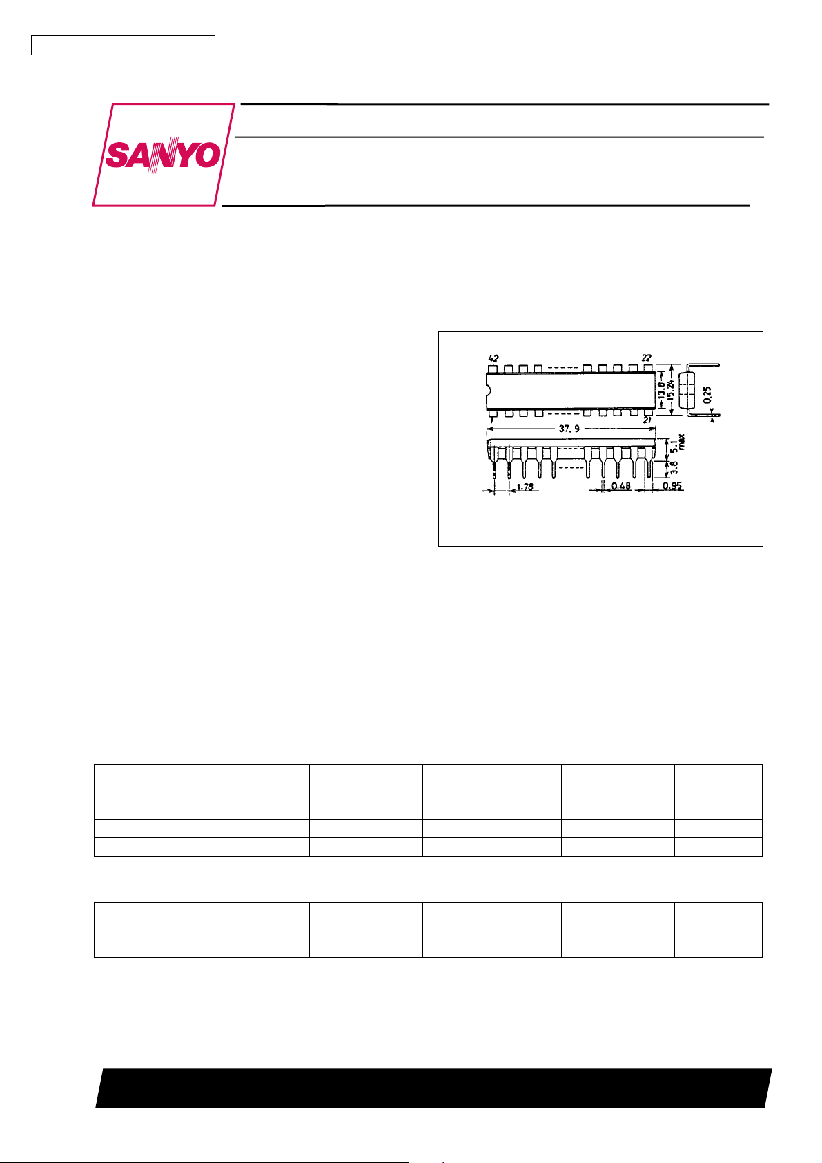
Package Dimensions
unit: mm
3025B-DIP42S
[LA7191N]
SANYO : DIP42S
Specifications
Maximum Ratings at Ta = 25°C
Parameter Symbol Conditions Ratings Unit
Maximum supply voltage V
Allowable power dissipation Pd max Ta %65°C 1020 mW
Operating temperature Topr –10 to +65 °C
Storage temperature Tstg –40 to +150 °C
Operating Conditions at Ta = 25°C
Parameter Symbol Conditions Ratings Unit
Recommended supply voltage V
Operating supply voltage range V
max 7.0 V
CC
CC
op 4.8 to 5.5 V
CC
5.0 V
SANYO Electric Co.,Ltd. Semiconductor Bussiness Headquarters
TOKYO OFFICE Tokyo Bldg., 1-10, 1 Chome, Ueno, Taito-ku, TOKYO, 110 JAPAN
22896HA (II) No.5471 - 1/11
Page 2
LA7191N
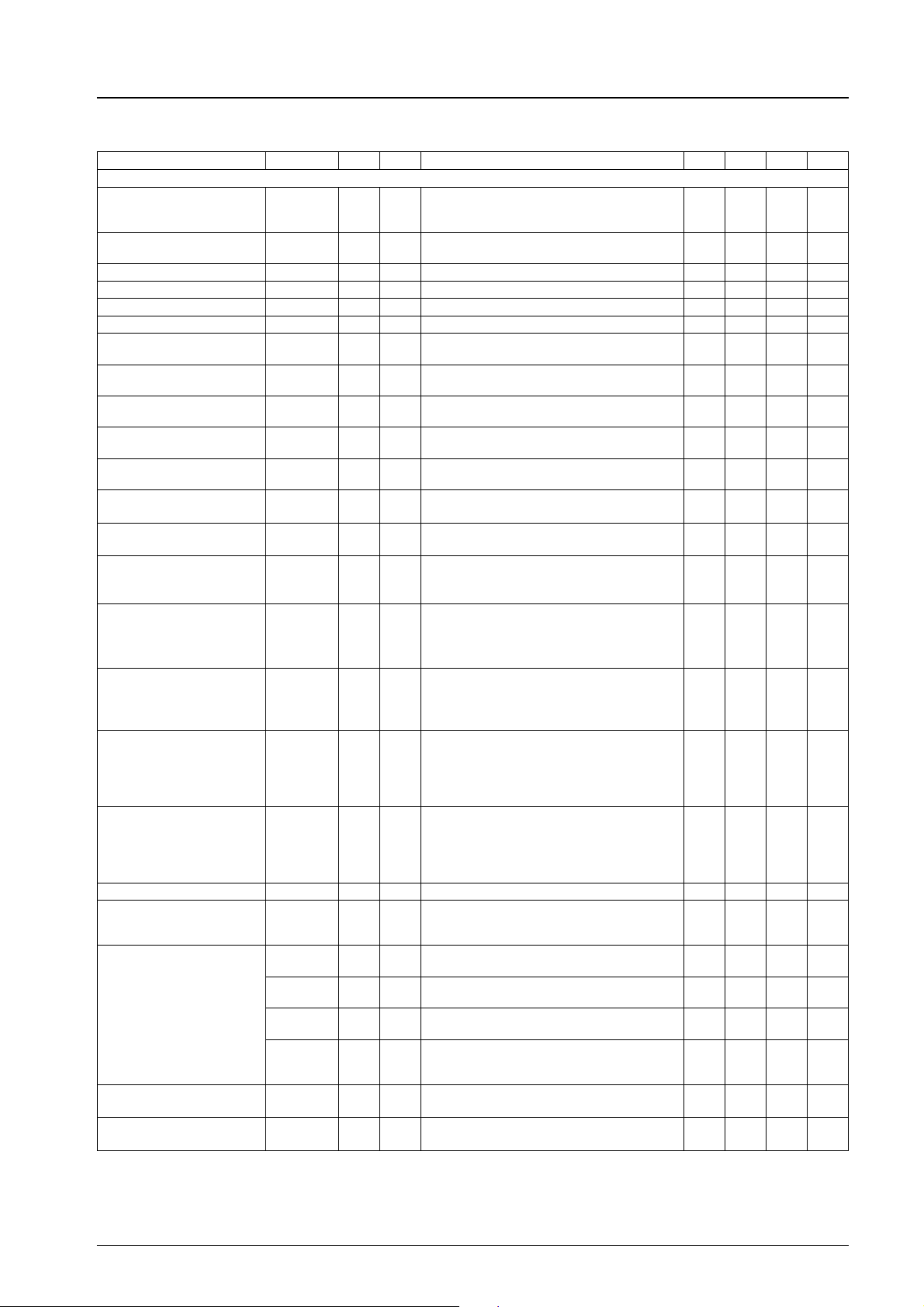
Operating Characteristics at Ta = 25°C, VCC= 5.0 V
Parameter Symbol Input
Output
Conditions min typ max Unit
[REC Mode Y]
Current drain REC I
CCR
When VCC= 5 V (when there is no signal),
measure sum of incoming current at pins 35
95 120 145 mA
and 28
AGC adjustment C
AGC
T37A VIN= 1.0 Vp-p video signal, use VR39 to
adjust T4 output to 0.5 Vp-p
VCA control characteristics VCA T37A T4 Measure T4 output level when S10 is set to 2 0.48 0.5 0.52 Vp-p
AGC adjustment voltage V
AGC
AGC detection voltage V
EE output level V
AGC Output 1 AGC 1 T37A T4 V
AGC Output 2 AGC 2 T37A T4 V
AGC Output 3 AGC 3 T37A T4 V
AGC Output 4 AGC 4 T37A T4 V
Sync separation output level V
Sync separation output
SYR
PW
pulse width
Sync separation output
∆ T
leading edge delay time
Sync separation threshold
TH
level
T37A T39 Measure T39 DC voltage in above state 3.2 3.4 3.6 V
T37A T38 Measure T38 DC voltage in same manner 1.2 1.4 1.6 V
AD
T37A T34A Measure T34A output level in same manner 0.95 1.00 1.05 Vp-p
EE
T37A T32 VIN= 1.0 Vp-p video signal,
= 2.0 Vp-p video signal
IN
Measure T4 output level
= 0.5 Vp-p video signal
IN
Measure T4 output level
= 700 mVp-p LUMI, 600 mVp-p SYNC
IN
Measure T4 SYNC level
= 700 mVp-p LUMI, 150 mVp-p SYNC
IN
Measure T4 SYNC level
500 540 560 mVp-p
470 490 500 mVp-p
135 150 165 mVp-p
70 85 100 mVp-p
4.0 4.2 4.4 Vp-p
Measure T32 output pulse wave high value
T37A T32 VIN= 1.0 Vp-p video signal,
SYR
T37A T32 VIN= 1.0 Vp-p video signal, measure delay
SYR
T37A T32 Gradually attenuate the input level, measure
SYR
Measure T32 output pulse width
time of output SYNC versus input SYNC
input level at point when output pulse width
4.4 4.7 5.0 µs
0.6 0.8 1.0 µs
–18 –14 dB
widens 1 µs or more beyond PWSYR
Sync tip level,
pedestal level,
white level measurement
(REC)
Pseudo V insertion level
(REC)
Pseudo H insertion level
(REC)
White insertion level (REC) ∆ WHR T37A T34 Measure T34 DC voltage when 1.3 V is
L
VOR
T37A T34 Measure electric potential for each of the T34
video output sync tip, pedestal, and white
peak, and assign the measured values to
L
SYN,LPED
, and L
, respectively
WHI
∆ VDR T37A T34 Measure T34 DC voltage when5Visapplied
to T33, and assign the measured value to
L
and calculate the difference with L
VDR
∆VDR=L
SYN–LVDR
SYN
∆ HDR T37A T34 Measure T34 DC voltage when 2.7 V is
applied to T33, and assign the measured
value to L
with L
PED
∆HDR=L
and calculate the difference
HDR
PED–LHDR
–80 0 +80 mV
–200 –100 0 mV
150 250 350 mV
applied to T33, and assign the measured
VCA detection voltage V
REC YNR operation
VR-YNR T37A T3 V
EP/LP
Y-LPF frequency
YLPF 1 T37A T3 V
characteristics
YLPF2 T37A T3 V
YLPF3 T37A T3 V
YLPF4 T37A T3 V
VCA
value to L
with L
WHI
∆WHR=L
T37A T9 Measure T9 DC voltage 3.1 3.4 3.7 V
= white 50% + CW
IN
(15.8 mVp-p) ratio between 32f
and 32.5f
= standard multiburst signal 1 Vp-p,
IN
2 MHz response to 500 kHz at T3
= standard multiburst signal 1 Vp-p,
IN
4.8 MHz response to 500 kHz at T3
= standard multiburst signal 1 Vp-p,
IN
2 MHz response to 500 kHz at T3, T22A: 5 V
= standard multiburst signal 1 Vp-p,
IN
4.8 MHz response to 500 kHz at T3, T22A:
and calculate the difference
WHR
WHI–LWHR
component
H
component
H
3.5 4.5 5.5 dB
0.2 0.7 1.2 dB
–4.5 –3.5 –2.5 dB
0.4 0.9 1.4 dB
–5.0 –4.0 –3.0 dB
5V.
FM modulator output level V
FM modulator secondary
H
distortion
FM
MOD
T40 No input, use VR42 to adjust output
frequency to 4 MHz, measure output level
T40 Ratio of 8 MHz component to 4 MHz in the
above state
0.8 1.0 1.2 Vp-p
–40 –35 dB
Continued on next page.
No. 5471 - 2/11
Page 3

Continued from preceding page.
LA7191N
Parameter Symbol Input
FM modulator modulation
sensitivity
S
MOD
Output
Conditions min typ max Unit
T4 T40 Measure amplitude of change in output
frequency when 2.6 V DC or 3.1 V DC is
applied to T4, 2 x (f3.1 – f2.6)
FM modulator linearity L
1/2 f
carrier shift CS1 T40 Measure amplitude of change in output
H
MOD
T4 T40 Measure output frequency when 2.85 V DC
applied to T4,
L
f2.85 – (f3.1 + f2.6)/2
=
MOD
S
MOD
frequency when SW41B is off and SW41A is
switched from on to off
CS2 T40 Measure amplitude of change in output
frequency when SW41B is on and SW41A is
switched from on to off
Emphasis gain G
EMPH
T4A T5 VIN= 0.5 Vp-p 10 kHz sine wave
Measure ratio of levels of input and output
amplitude at T5
Detail enhancer
characteristics
Nonlinear emphasis
characteristics
Main linear emphasis
characteristics
White clipping level L
Dark clipping level L
Non-linear emphasis
characteristics SP
G
ENH1
T4A T5 VIN= 158 mVp-p 2 MHz sine wave
Measure ratio of levels of T5 and T4,
difference with G
G
ENH2
T4A T5 VIN= 50 mVp-p 2 MHz sine wave
Measure ratio of levels of T5 and T4,
difference with G
G
ENH3
T4A T5 VIN= 15.8 mVp-p 2 MHz sine wave
Measure ratio of levels of T5 and T4,
difference with G
G
ENH4
T4A T5 VIN= 15.8 mVp-p 2 MHz sine wave
Measure output amplitude at T5 in edit mode,
difference with G
G
NLEMP1
T4A T5 VIN= 500 mVp-p 2 MHz
Measure ratio of levels of T5 and T4,
difference with G
G
NLEMP2
T4A T5 VIN= 158 mVp-p 2 MHz
Measure ratio of levels of T5 and T4,
difference with G
G
NLEMP3
T4A T5 VIN= 50 mVp-p 2 MHz
Measure ratio of levels of T5 and T4,
difference with G
G
ME1
T4A T5 VIN= 50 mVp-p 200 kHz sine wave
Measure ratio of levels of T5 and T4,
difference with G
G
ME2
T4A T5 VIN= 50 mVp-p 2 MHz
Measure ratio of levels of T5 and T4,
difference with G
WC
DC
T4A T5 VIN= 500 mVp-p white 100% video signal
Measure white clipping level at T5
T4A T5 VIN= 500 mVp-p white 100% video signal
Measure dark clipping level at T5
NLE-SP T4A T5 Same as G
EMPH
EMPH
EMPH
EMPH
EMPH
EMPH
EMPH
EMPH
EMPH
NLEMP3
[PB Mode Y]
Current drain PB I
Dropout compensation
period
P Incoming current at pins 35 and 28 when
T
CC
DOC
T39A
T4A
V
= 5.0 V
CC
T34A T39A: 4 MHz, 300 mVp-p sine wave
T4A: 0.5Vp-p video signal
T34A: time from when input went to 0 until
T34A output returned, SW10 → 1
DOC loop gain GDOC T39A
T12 T39A: 4 MHz, 300 mVp-p sine wave
T4A
T4A: 0.5Vp-p video signal
T39A: Input/output response when 5H have
elapsed after input went to 0, SW10 → 3
FM demodulation voltage V
FM demodulation sensitivity S
DEM4
DEM
T39A T3 VIN=300 mVp-p,f=4MHz, Output DC
voltage
T39A T3 VIN= 300 mVp-p,f=2MHz, V
VIN= 300 mVp-p,f=6MHz, V
Calculate S
DEM
=(V
DEM6–VDEM2
x 100
DEM2
DEM6
)/4
1.6 2.0 2.4
MHz/V
–2 0 +2 %
6.8 7.8 9.5 kHz
6.8 7.8 9.5 kHz
–0.5 0 +0.5 dB
0.9 1.4 1.9 dB
2.2 3.2 4.2 dB
4.0 5.0 6.0 dB
1.8 2.8 3.8 dB
0.5 1.4 2.3 dB
2.6 3.8 5.2 dB
4.9 6.4 7.9 dB
4.9 5.2 5.5 dB
13.1 13.6 14.1 dB
186 193 200 %
–60 –55 –50 %
3.0 4.0 5.0 dB
125 155 185 mA
0.35 0.5 0.65 ms
–1.0 0 +1.0 dB
1.5 2.0 2.5 V
0.36 0.45 0.54
V/MHz
Continued on next page.
No. 5471 - 3/11
Page 4
Continued from preceding page.
LA7191N
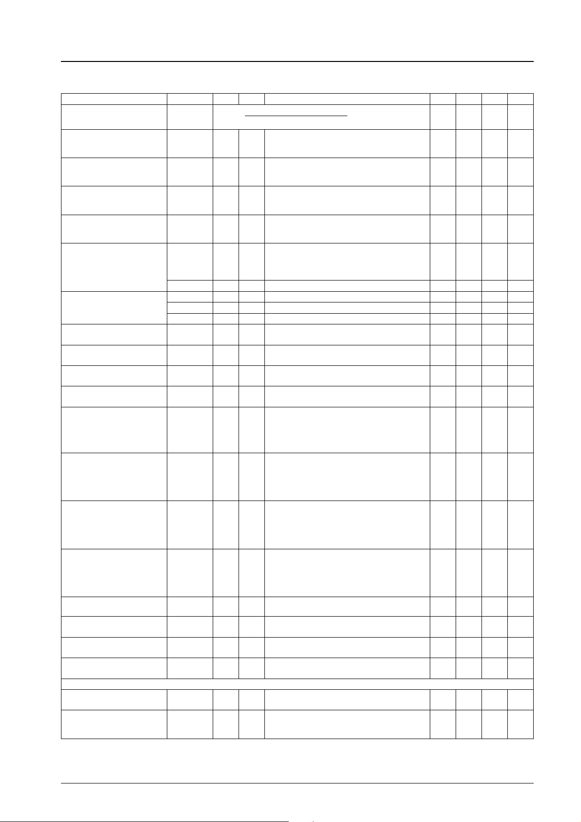
Parameter Symbol Input
FM demodulation linearity L
DEM
Carrier leak CL T39A T3 V
PB YNR characteristics
GP-YNR T4A T28A V
LP/EP
PB LNC characteristics
GP-LNC T4A T28A V
SP
Playback through gain G
PB
L
DEM
Output
V
DEM4
=
–(V
DEM6+VDEM2
V
DEM6–VDEM2
= 300 mVp-p,f=4MHz
IN
Ratio between 4 MHz component of T3 and
S
DEM
= white 50% + CW (15.8 mVp-p)
IN
Ratio between 32f
component
= white 50% + CW (15.8 mVp-p)
IN
Ratio between 32f
component
Conditions min typ max Unit
)/2
x 100
component and 32.5f
H
component and 32.5f
H
T4A T34A Apply VIN= 0.5 Vp-p video signal to pin 4,
and determine ratio between T34A output
level and input level
Nonlinear de-emphasis
characteristics
GNL
DEEM1
T4A T34A VIN= white 50% + CW
(f = 1 MHz, 158 mVp-p)
measure input/output response, difference
with GPB
Noise canceller
characteristics
PIC-CTL center response
characteristics
PIC-CTL hard response
characteristics
PIC-CTL soft response
characteristics
Nonlinear de-emphasis
characteristics SP
Sync tip level,
pedestal level,
white level measurement
(PB)
Pseudo V insertion level
(PB)
Pseudo H insertion level
(PB)
GNL
DEEM2
G
WNC1
G
WNC2
G
WNC3
G
PC
G
PH
G
PS
NLDE-SP T4A T34A Same as GNL
L
VOR
∆ VDP T4A T34 Measure pin 34 DC voltage when5Vis
∆ HDP T4A T34 Measure pin 34 DC voltage when 2.7 V is
T4A T34A f = 1 MHz, 50 mVp-p –5.0 –4.0 –3.0 dB
T4A T34A f = 1.5 MHz, 158 mVp-p –1.3 –0.8 –0.3 dB
T4A T34A f = 1.5 MHz, 50 mVp-p –4.5 –3.5 –2.5 dB
T4A T34A f = 1.5 MHz, 15.8 mVp-p –10.5 –9.0 –7.5 dB
T4A T34A f = 2 MHz, 158 mVp-p 1.2 1.7 2.2 dB
T4A T34A f = 2 MHz, 158 mVp-p 7.0 8.0 10.0 dB
T4A T34A f = 2 MHz, 158 mVp-p –10.0 –8.0 –7.0 dB
DEEM2
T4A T34 With VIN= white 100% and T34A at 1.0
Vp-p, measure electric potential for each of
the pin 34 video output sync tip, pedestal,
and white peak, and assign the measured
values to L
SYN,LPED
, and L
, respectively
WHI
applied to pin 33, and assign the measured
value to L
with L
∆ VDP = L
, and calculate the difference
VDP
SYN
SYN–LVDP
applied to pin 33, and assign the measured
value to L
with L
∆HDP = L
, and calculate the difference
HDP
PED
PED–LHDP
White insertion level (PB) ∆WHP T4A T34 Measure pin 34 DC voltage when 1.3 V is
applied to pin 33, and assign the measured
Sync separation output level V
Sync separation output
PW
pulse width
Sync separation output
∆ T
leading edge delay time
4.2 V regulator operation
check
V
SYP
SYP
SYP
REG
value to L
with L
∆WHP = L
T4A T32 VIN= 0.5 Vp-p video signal, pin 32 output
pulse wave high value
T4A T32 VIN= 0.5 Vp-p video signal, T32 output pulse
width
T4A T32 VIN= 0.5 Vp-p video signal, measure delay
time of output SYNC versus input SYNC
T30 Measure DC level of T30 in REC mode 3.95 4.15 4.35 VDC
, and calculate the difference
WHP
WHI
WHI–LWHP
[REC Mode Chroma]
REC chroma low-band
conversion output level
Burst emphasis amount
(NTSC mode)
V
OR-15
T37A T15A VIN= standard color bar signal (1 Vp-p),
measure burst level at T15A
GBE T37A T15A VIN= standard color bar signal (1 Vp-p)
Ratio of burst level at T15A when S41A is off
(SP/EP) and on (LP)
–3.5 0 +3.5 %
–40 –35 dB
–11 –9 –7 dB
H
–7.0 –5.5 –4.0 dB
H
4.0 5.5 7.0 dB
–2.8 –1.8 –0.8 dB
–5.0 –4.0 –3.0 dB
–80 0 +80 mV
–300 –200 –100 mV
20 120 220 mV
4.0 4.2 4.4 Vp-p
4.4 4.7 5.0 µs
0.9 1.1 1.3 µs
120 160 200
5.5 6.0 6.5 dB
mVp-p
Continued on next page.
No. 5471 - 4/11
Page 5
Continued from preceding page.
LA7191N
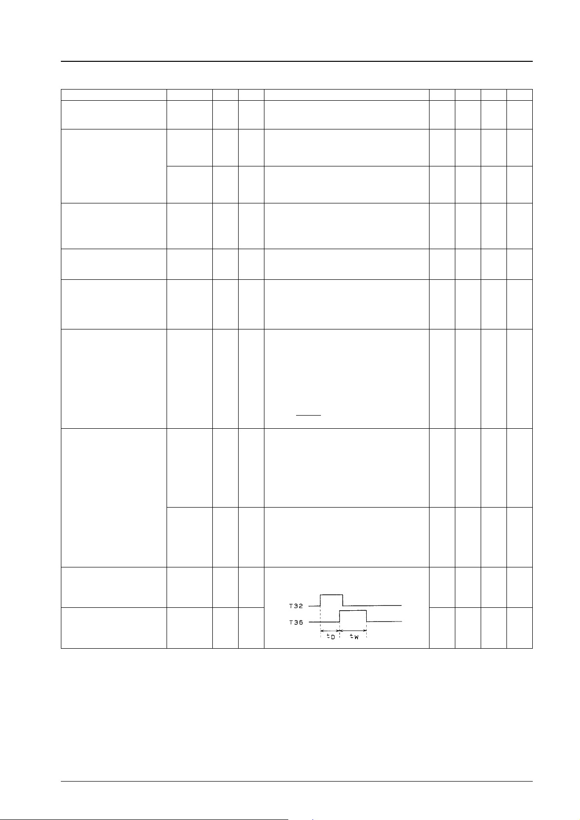
Parameter Symbol Input
VXO oscillation level V
VXO-R
REC ACC characteristics ACC
ACC
REC ACC killer input level VACC
REC ACC killer output level VO
Input level for REC ACC
killer return
VXO control sensitivity S
REC APC pull-in range ∆ f
V
ACCK-OFF
VXO
APC1
∆ f
APC2
BGP delay time t
R1
R2
K-ON
ACCK
D
Output
Conditions min typ max Unit
T37A T19 VIN= standard color bar signal (1 Vp-p),
measure T19 output amplitude (with a FET
probe)
T37A T15A VIN= standard color bar signal (1 Vp-p),
input +6 dB chroma signal level only,
measure T15A burst level, and calculate ratio
with V
OR
-15
T37A T15A VIN= standard color bar signal (1 Vp-p),
input –6 dB chroma signal level only,
measure T15A burst level, and calculate ratio
with V
OR
-15
T37A T15A VIN= standard color bar signal (1 Vp-p),
lower the chroma signal, and measure the
input burst level at the point where output at
T15A ceases, and calculate the ratio with the
standard input level
T37A T15A Use a spectrum analyzer to measure the
output level at T15A in the killer state
described previously; ratio with V
OR-15
T4A T34A Starting from the killer state described
previously, gradually raise the input chroma
level and measure the input burst level when
output is generated at T15A and calculate the
ratio with the standard input level
T37A T17
Measure the pin 17 DC voltage when a
T19A
standard color bar signal is input
(1 Vp-p)...V
Measure the frequency at T19A when V0is
0
applied to pin 17 from the external power
supply...f
Measure the frequency at T19A when V0+
10 mV is applied to pin 17...f
S
VXO
=
1
f
2–f1
10
2
Hz/mV
T37A T15A Input a 50% white signal overlapped with a
4.4336 MHz, 300 mVp-p continuous wave.
After confirming that there is output at T15A,
increase the frequency of the CW until the
output at T15A stops, and then gradually
reduce the frequency until output appears
again at T15A; that CW frequency is f1.
∆f
= f1 – 4433619 (Hz)
APC1
T37A T15A In the same manner, reduce the frequency of
the CW until the output at T15A stops, and
then gradually increase the frequency until
output appears again at T15A; that CW
frequency is f2.
∆f
= f2 – 4433619 (Hz)
T37A T32
APC2
Measure waveforms at T32 and T36 when a
T36
standard color bar signal (1 Vp-p) is input.
450 560 670
mVp-p
0.2 0.5 dB
–0.5 –0.1 dB
–26 dB
–60 –50 dB
–20 dB
3.8 5.7 7.6
Hz/mV
350 440 Hz
–900 –350 Hz
4.3 µs
BGP pulse width t
W
T37A T32
T36
4.8 µs
Continued on next page.
No. 5471 - 5/11
Page 6
Continued from preceding page.
LA7191N
Parameter Symbol Input
REC AFC pull-in range ∆f
∆ f
AFC1
AFC2
[PB Mode Chroma]
PB chroma video output
Vop-34 T39A
level
PB chroma pin 31 output
Vop-31 T39A
level
PB ACC characteristics ACC
ACC
PB killer input level V
PB killer chroma output
level
PB main converter carrier
ACK-P
V
OACK-P
C
leak
Burst de-emphasis amount
GBD T39A
(NTSC mode)
PB XO output level V
PB XO oscillation frequency
XO-P
∆ f
variation
Output
Conditions min typ max Unit
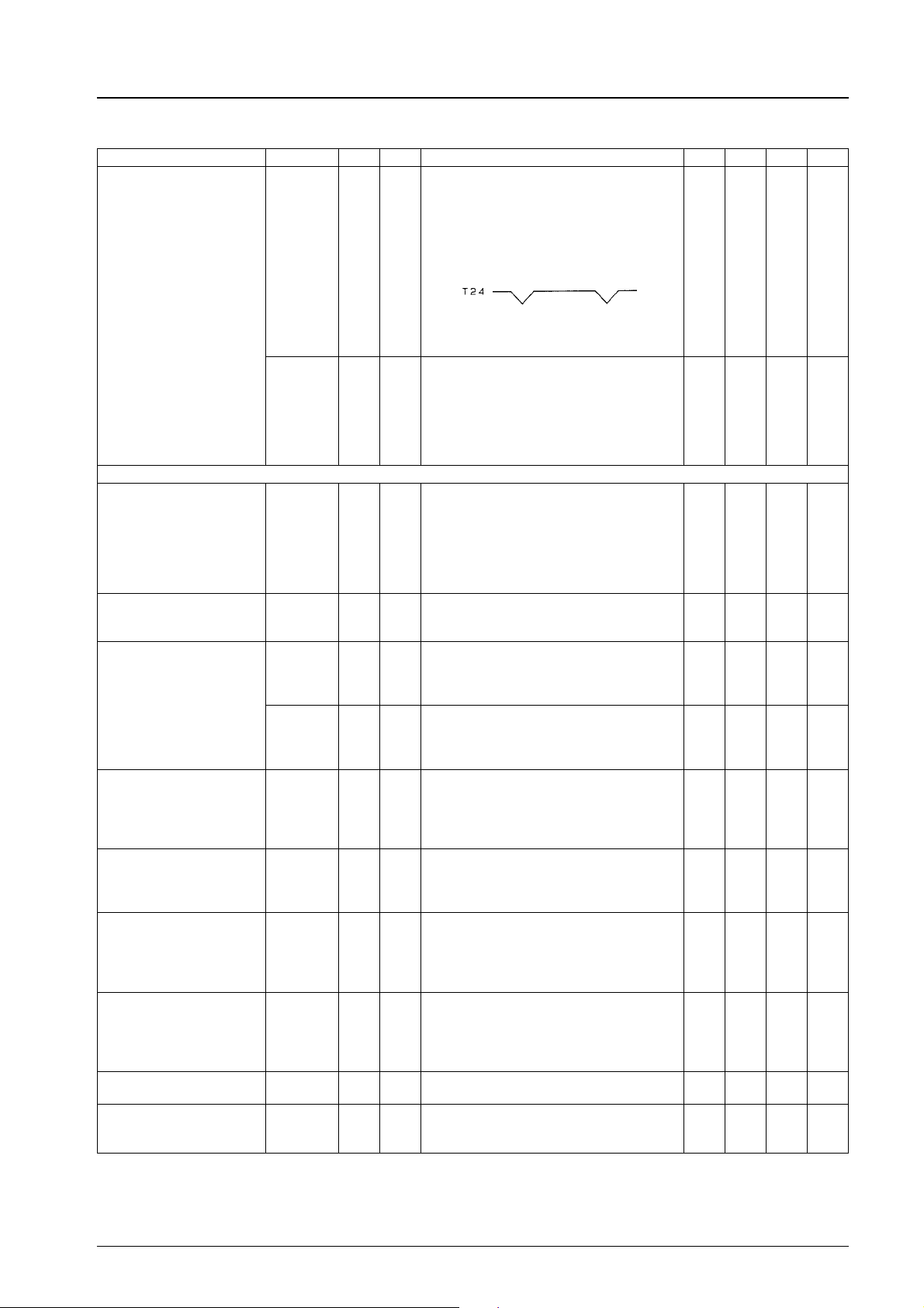
T37A T24 Input a string of pulses (negative polarity) at
300 mV, 15.6 kHz with a width of 5 µs. After
increasing the frequency of the pulse string
until the waveform at pin 24 is disrupted,
then reduce the frequency until the waveform
at pin 24 is normal again; that pulse string
frequency is f
∆f
AFC1=f1
.
1
– 15.625 (kHz)
T37A T24 In the same manner, after reducing the
frequency of the pulse string until the
waveform at pin 24 is disrupted, then
increase the frequency until the waveform at
pin 24 is normal again; that pulse string
frequency is f
∆f
AFC2=f2
.
2
– 15.625 (kHz)
T34A In PB, SP mode, input a 4 MHz: 300 mVp-p
T15A
T4A
continuous wave at T39A, and from T15A
input a chroma signal (SP mode, burst 50
mVp-p) that underwent low-band conversion
from a chroma noise test signal.
Input a 50% white signal from T4A and
measure the T34A burst level
T31 Measure the T31 burst level under the same
T15A
conditions as for Vop-34.
T4A
T39A
P1
T31 Input the input chroma level at +6 dB under
T15A
T4A
the same conditions as for Vop-34 and
measure the T31 burst level, and calculate
the ratio with Vop-31.
T39A
P2
T31 Input the input chroma level at –6 dB under
T15A
T4A
the same conditions as for Vop-34 and
measure the T31 burst level, and calculate
the ratio with Vop-31.
T39A
T31 Lower the input chroma level under the same
T15A
T4A
conditions as for Vop-34 and measure the
input burst level at the point where T31
chroma output ceases. (Calculate ratio with
standard input of 50 mVp-p)
T39A
T34A Use a spectrum analyzer to measure the T34
T15A
T4A
chroma output level in the killer state
described previously. Calculate ratio with
Vop-34.
T39A
LP
T34A Monitor T34A with a spectrum analyzer under
T14A
T4A
the same conditions as for Vop-34 and
calculate the ratio between the 4.43 MHz
component and the 5.06 MHz carrier leak
component.
T31 From T39A, input a 4 MHz 300 mVp-p
T4A
T27A
continuous wave; from T4A, input a 50%
white signal, and calculate the ratio between
the output level during the T31 burst interval
and the output level during other intervals.
T19 Measure the PB mode T19 output level with
an FET probe
XO
T19A Measure the frequency at T19A during PB
mode...f
∆f
= f – 4433619 (Hz)
XO
1.0 7.0 kHz
–3.7 –1.0 kHz
240 300 360 mVp-p
220 270 320 mVp-p
0.5 0.8 dB
–0.5 –0.2 dB
–40 –32 –25 dB
–44 –40 dB
–40 –33 dB
–4.40 –4.65 –4.90 dB
480 610 750
mVp-p
–9 0 +9 Hz
Continued on next page.
No. 5471 - 6/11
Page 7
Continued from preceding page.
LA7191N
Parameter Symbol Input
SLD detection current I
2fsc output level V2fsc T21 In PB mode, measure the T21 output level
SLD1
I
SLD2
Output
T39A
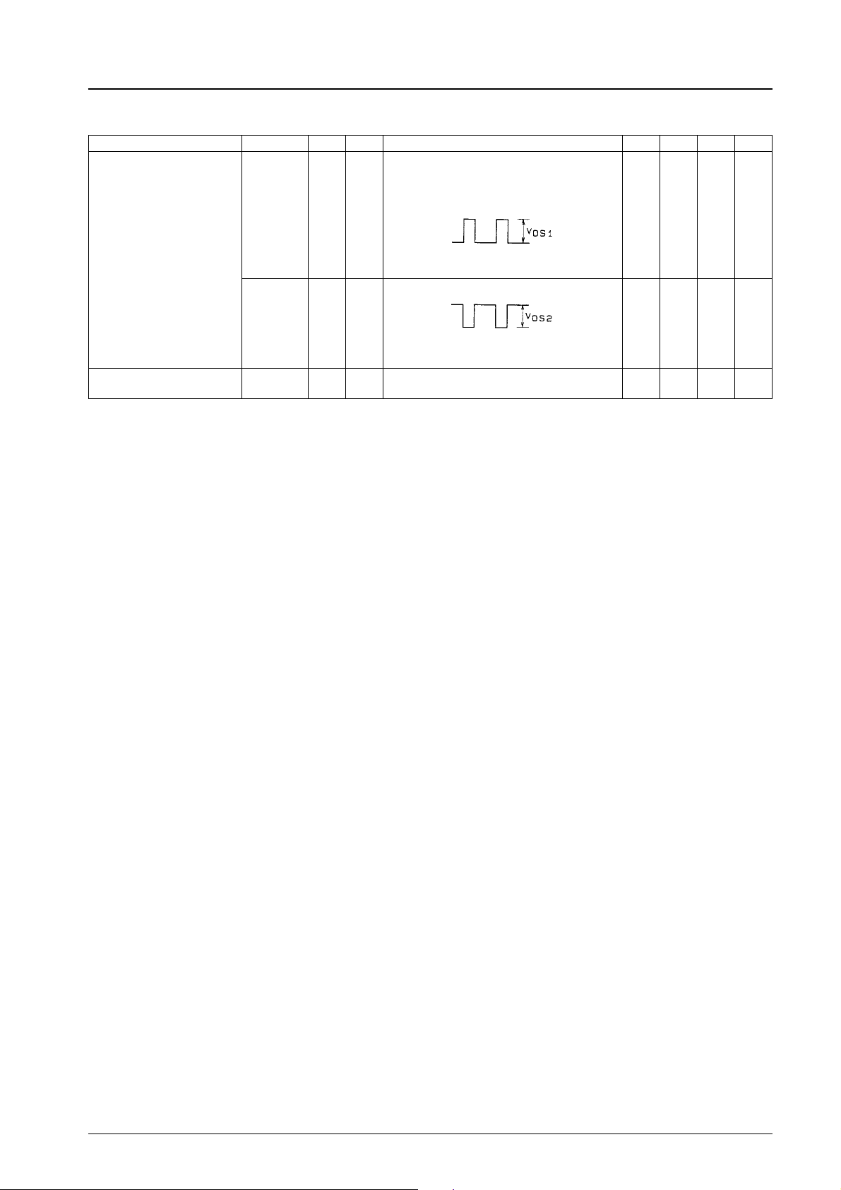
T23A In PB mode, with S24: 3 and S23: off, input a
T4A
T39A
T4A
4 MHz 300 mVp-p continuous wave from
T39A, input a 50% white signal from T4A,
and measure the wave peak at T23A
I
= VOS1/1 kΩ
SLD1
T23A Same as above (however, S24 = 1)
I
= VOS2/1 kΩ
SLD2
with an FET probe
Conditions min typ max Unit
135 µA
135 µA
480 640 800
mVp-p
Note) A trap (4.84 MHz for NTSC systems and 5.69 MHz for PAL systems) is required in the chroma playback system (between
pins 25 and 27 or between pins 31 and 29) in order to suppress unnecessary components in converter output.
No. 5471 - 7/11
Page 8
LA7191N
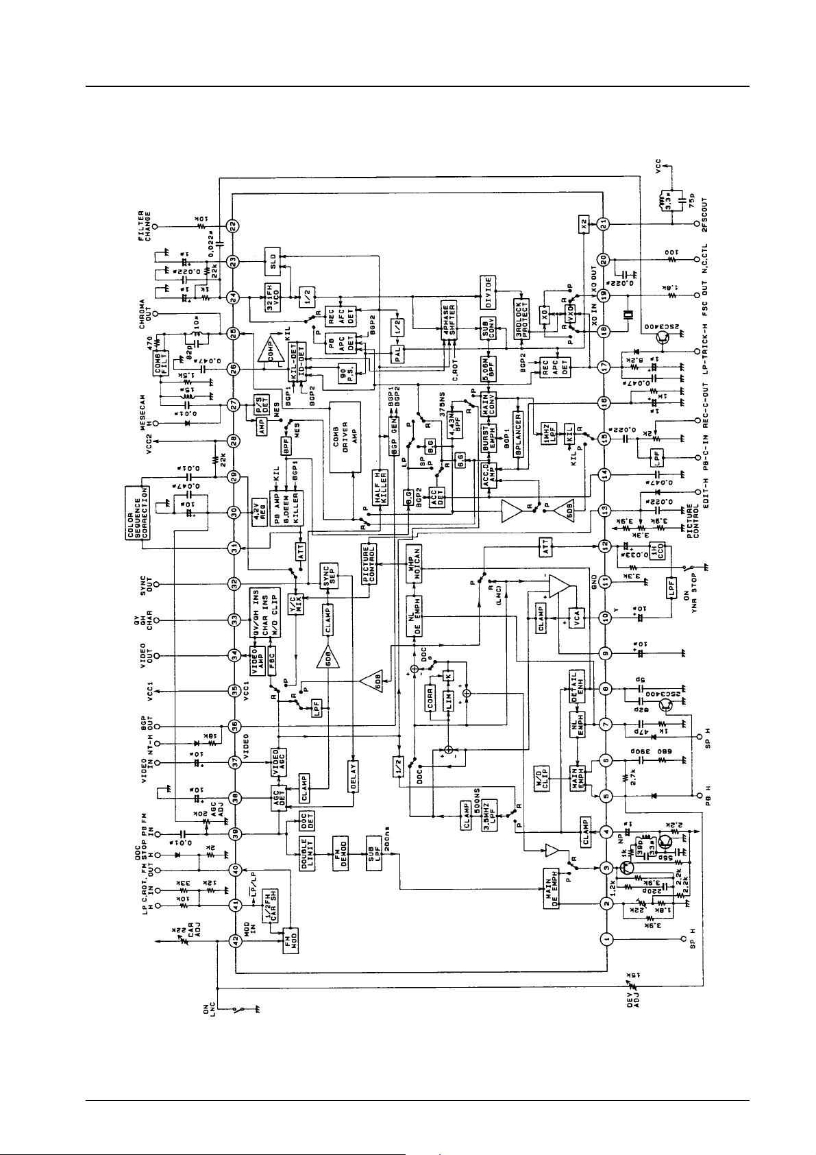
Equivalent Circuit Block Diagram and Sample Application Circuit
Unit (resistance: Ω, capacitance: F)
No. 5471 - 8/11
Page 9
LA7191N
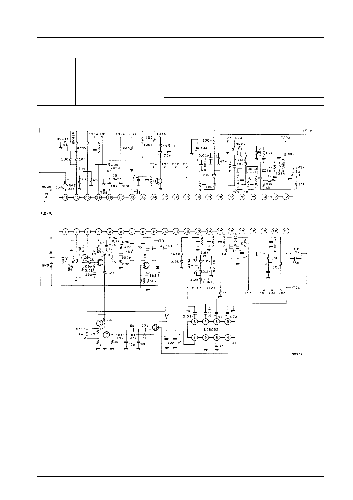
LA7191N Control Pins
Pin No. Function Control Contents
20 N.C control Linear When → high, N.C → Strong
22 Filter switching H 3.58 MHz system
L or OPEN 4.43 MHz system
42 YNR/LNC selection OPEN YNR
L LNC (line noise canceller)
Test Circuit Diagram
LA7191N
Unit (resistance: Ω, capacitance: F)
No. 5471 - 9/11
Page 10
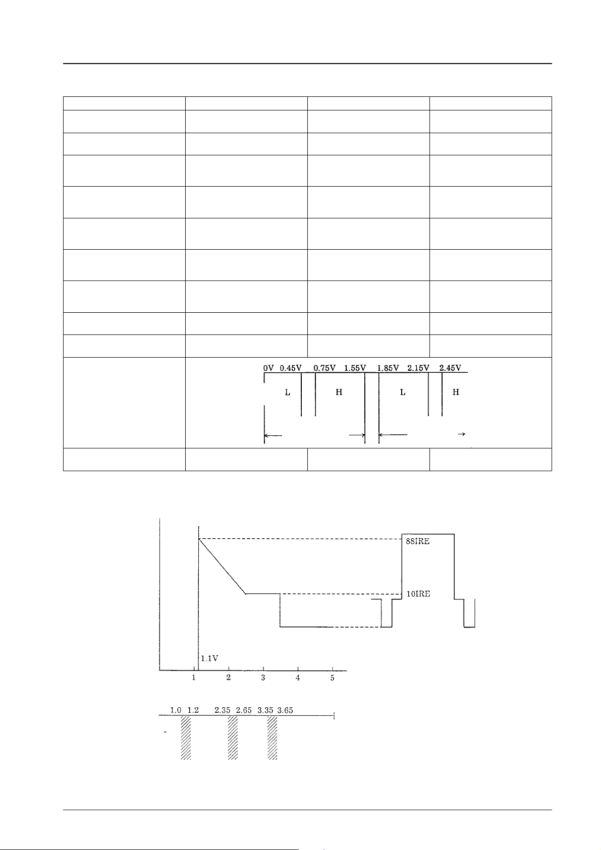
Control Pin Function Chart
Pin No. L M H
Pin 5
R/P switching
Pin 1
SP changeover
Pin13
EDIT2
PIC-CTL
Pin 14
SECAM
CTL
Pin 17
Special playback switching
Pin 27
MESECAM
CTL
Pin 33
QV, QH, CHAR
Pin 36
NTSC-CTL
Pin 40
DOC STOP control
Pin 41
ROTARY pulse
LP switch
LA7191N
Open
REC mode
Open Over 3.9 V
2Vto2.5V
PIC-CTL
SOFT
Open
Normal mode
ROTARY
PULSE
2.5Vto3V
PIC-CTL
HARD
Open
Before comb in SP
Open Over 3.0 V
Refer to Pin 33,
QV, QH, CHAR,
insertion diagram
Over 3.8V
Over 3.6 V
Over 4.0 V
SECAM mode
Over 3.5 V
(over 200 µA)
After comb in SP
MESECAM mode
NTSC mode if current is
150 µA or more
Over 3.9 V
DOC STOP
PB mode
SP mode
EDIT ON
Pin 42
YNR/LNC switch
Pin 33
QV, QH, CHAR, insertion
Pin 34 output voltage
Through
Tape
speed SP or EP mode LP mode
Line NC when
under1VinPB
SP: LNC, LP/EP: YNR
Open
Pin 33 control voltage
(V)
THROUGH CHAR QH QV
No. 5471 - 10/11
Page 11

LA7191N
No products described or contained herein are intended for use in surgical implants, life-support systems, aerospace equipment,
nuclear power control systems, vehicles, disaster/crime-prevention equipment and the like, the failure of which may directly or
indirectly cause injury, death or property loss.
Anyone purchasing any products described or contained herein for an above-mentioned use shall:
1 Accept full responsibility and indemnify and defend SANYO ELECTRIC CO., LTD., its affiliates, subsidiaries and distributors
and all their officers and employees, jointly and severally, against any and all claims and litigation and all damages, cost and
expenses associated with such use:
2 Not impose any responsibility for any fault or negligence which may be cited in any such claim or litigation on SANYO
ELECTRIC CO., LTD., its affiliates, subsidiaries and distributors or any of their officers and employees jointly or severally.
Information (including circuit diagrams and circuit parameters) herein is for example only; it is not guaranteed for volume
production. SANYO believes information herein is accurate and reliable, but no guarantees are made or implied regarding its use
or any infringements of intellectual property rights or other rights of third parties.
This catalog provides information as of February, 1996. Specifications and information herein are subject to change without notice.
No. 5471 - 11/11
 Loading...