

Page 1
Ordering number: EN1409B
Monolithic Linear IC
LA7220
Electronic Switch for VCR/Audio Use
Overview
The LA7220 is a 3-channel 2-position high-performance analog
switch having wide application from audio band to video band.
It is also provided with 2 channels of muting function.
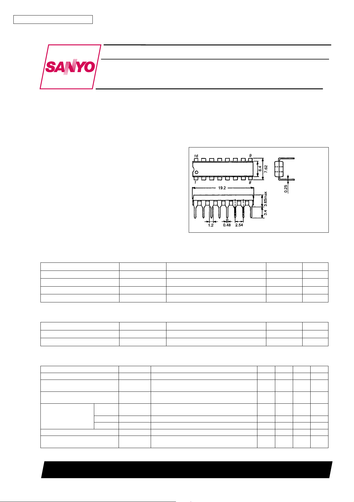
Package Dimensions
unit : mm
3006B-DIP16
[LA7220]
Features
.
3-channel 2-position switch
.
Wide input dynamic range
.
Low distortion
.
Good frequency characteristic
.
Muting available
SANYO : DIP16
Specifications
Maximum Ratings at Ta = 25°C
Parameter Symbol Conditions Ratings Unit
Maximum supply voltage V
Allowable power dissipation Pd max Ta % 65°C 500 mW
Operating temperature Topr –20 to +70 °C
Storage temperature Tstg –40 to +125 °C
max 15 V
CC
Operating Conditions at Ta = 25°C
Parameter Symbol Conditions Ratings Unit
Recommended supply voltage V
Operating voltage range V
CC
op 9to13 V
CC
Operating Characteristics at Ta = 25°C, VCC=12V
Parameter Symbol Conditions min typ max Unit
Current drain I
Total harmonic distortion THD
Noise voltage V
1ch CR1
Crosstalk
Pedestal level ∆Vped V
Maximum input voltage V
2ch CR2 Input 1: Rg = 50 Ω, (Note 2) –60 dB
3ch CR3 Input 1: Rg = 50 Ω, (Note 2) –50 dB
CC
NO
IN max
Rg = 600 Ω, 4.5 Vp-p,f=1kHz, R
(Note 1)
Rg = 600 Ω,f=20Hzto20kHz, RL= ∞,
(Note 1)
Input 1: Rg = 50 Ω, 2 Vp-p, f = 3.58 MHz,
Input 2: Rg = 500 Ω, (Note 2)
(Pins 10, 13, 15)=0to12V,(Note 1) –100
CTL
Rg = 600 Ω,f=1kHz, RL= ∞, THD = 1%,
(Note 1)
L
= ∞,
5.0 Vp-p
Continued on next page.
SANYO Electric Co.,Ltd. Semiconductor Bussiness Headquarters
TOKYO OFFICE Tokyo Bldg., 1-10, 1 Chome, Ueno, Taito-ku, TOKYO, 110 JAPAN
61096HA(II)/9068YT/8215KI,TS No.1409-1/6
12 V
30.0 39.9 mA
0.007 0.1 %
–93 –80 dBs
–50 dB
0 + 100
mV
Page 2
LA7220
Continued from preceding page.
Parameter Symbol Conditions min typ max Unit
2nd harmonic voltage H2
3rd harmonic voltage H3
Switch changeover voltage V
Mute threshold voltage
Crosstalk between
channels
1ch
2ch –50 –68 dB
3ch –50 –68 dB
CTLS
V
ML
V
MH
Mute compression ratio
Control pin flow-in current I
Input impedance Z
Output impedance Z
(Pin 1) V
(Pin 2) V
(Pin 5) V
(Pin 6) V
(Pin 7) V
Pin voltage
(Pin 8) V
(Pin 9) V
(Pin 12) V
(Pin 16) V
CTL
IN
OUT
pin1
pin2
pin5
pin6
pin7
pin8
pin9
pin12
pin16
Note 1. Measurements are made for each of 1ch, 2ch, 3ch using input A and input B.
Input A: V
Input B: V
(pins 10, 13, 15) is 12 V at the measurement mode.
CTL
is 0 V at the measurement mode.
CTL
Rg=50Ω, 4.0 Vp-p,f=1MHz, R
(Note 1)
Rg=50Ω, 4.0 Vp-p,f=1MHz, R
(Note 1)
(Note 1) 2.6 3.1 4.0 V
Low level, (Note 3) 1.1 1.5 1.9 V
High level, (Note 3) 6.6 7.3 8.0 V
Rg = 500 Ω,R
Rg=50Ω, 2 Vp-p, f = 3.58 MHz, (Note 4)
=∞, other channel input
L
Rg = 600 Ω, 2 Vp-p,f=1kHz,
R
= ∞, series resistance 10 kΩ, (Note 3)
L
(Note 1) 8 µA
(Note 1) 10 kΩ
(Note 1) 29 Ω
V
=0V
pin15
V
= 12 V 7.9 V
pin15
Test point: V14
Test point: V2 7.2 V
V
=0V
pin13
V
= 12 V 7.9 V
pin13
Test point: V16
Test point: V5 7.2 V
Test point: V7 7.2 V
V
=0V
pin10
V
= 12 V 7.9 V
pin10
V
=0V
pin10
V
= 12 V 7.9 V
pin10
V
=0V
pin13
V
= 12 V 7.9 V
pin13
V
=0V
pin15
V
= 12 V 7.9 V
pin15
Test point: V18
Test point: V17
Test point: V15
Test point: V13
L
L
= ∞,
= ∞,
–46 –55 dB
–46 –55 dB
–50 –68 dB
–60 dB
7.9 V
7.9 V
7.9 V
7.9 V
7.9 V
7.9 V
2. Measurements are made using input A and B.
3. Measurements are made for 1ch, 3ch.
4. Measurements are made for each of 1ch, 2ch, 3ch using input A and B on other channels.
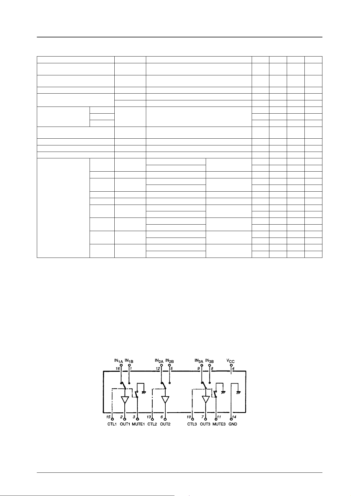
Equivalent Circuit Block Diagram
No.1409-2/6
Page 3
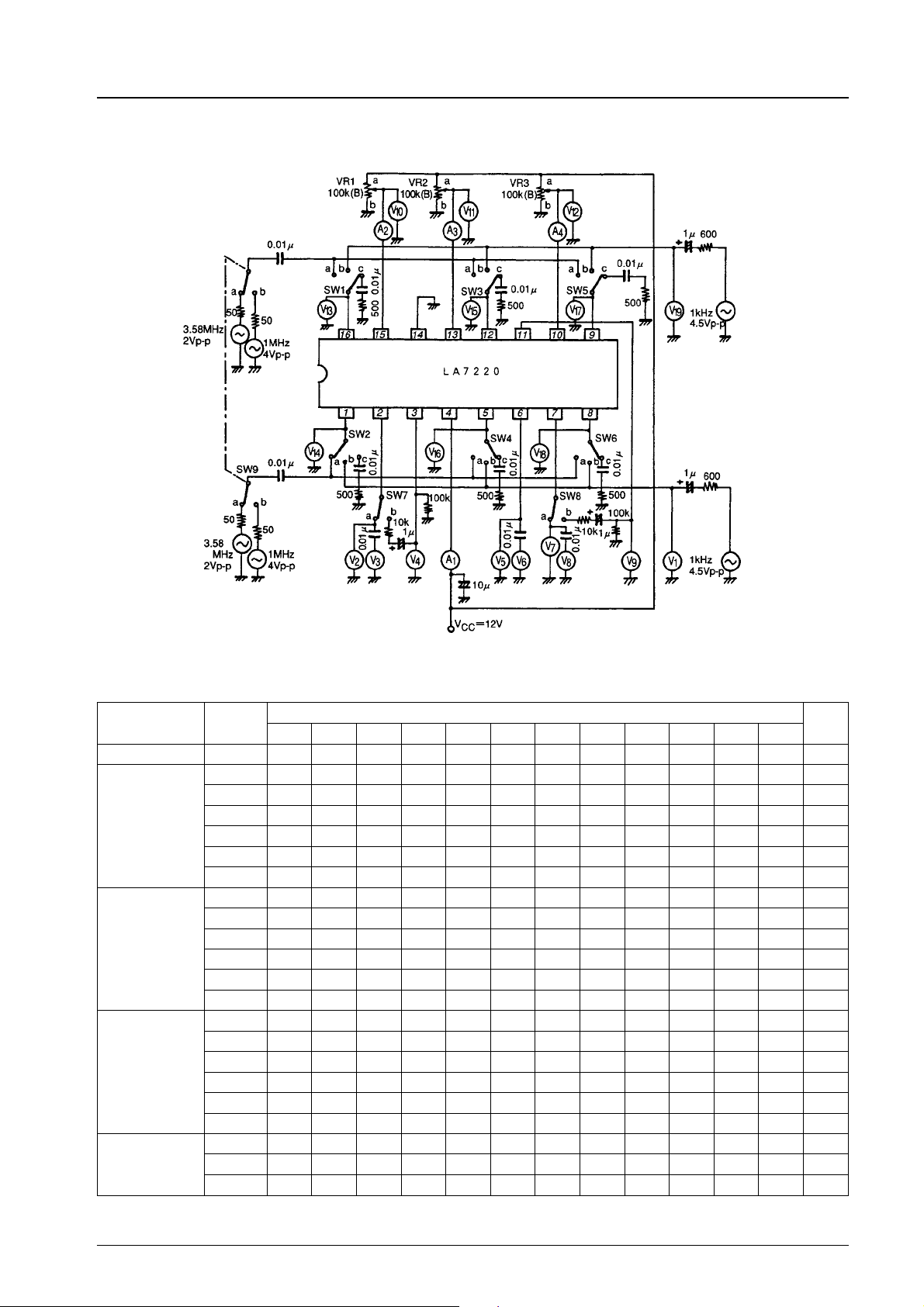
Test Circuit
LA7220
Unit (resistance: Ω, capacitance: F)
Test Conditions
Item Symbol
Current drain I
Total
harmonic
distortion
Noise 1chA V
Crosstalk 1chA CR c a ccccaaaabbV3
Pedestal
level
1chA THD b cccccaaaabbV3
1chB THD c b ccccaaabbbV3
2chA THD c c b c c c aaababV6
2chB THD c c c b c c aaabbbV6
3chA THD ccccbcaaabbaV8
3chB THD cccccbaaabbbV8
1chB V
2chA V
2chB V
3chA V
3chB V
1chB CR a cccccaaabbbV3
2chA CR c c c a c c aaababV6
2chB CR c c a c c c aaabbbV6
3chA CR cccccaaaabbaV8
3chB CR ccccacaaabbbV8
1ch ∆V
2ch ∆V
3ch ∆V
SW1 SW2 SW3 SW4 SW5 SW6 SW7 SW8 SW9 VR1 VR2 VR3
CC
NO
NO
NO
NO
NO
NO
PED
PED
PED
ccccccaaabbbA1
ccccccaaaabbV3
ccccccaaabbbV3
ccccccaaababV6
ccccccaaabbbV6
ccccccaaabbaV8
ccccccaaabbbV8
ccccccaaaa/bbbV2
ccccccaaaba/bbV5
ccccccaaabba/bV7
SW, VR mode
Test
point
No.1409-3/6
Page 4
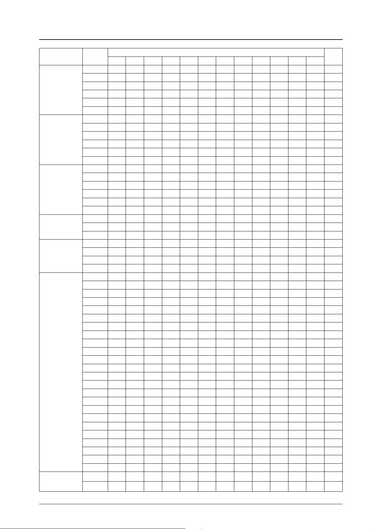
LA7220
Item Symbol
Maximum
input
voltage
2nd
harmonic
voltage
3rd
harmonic
voltage
Switch
changeover
voltage
Mute
threshold
Crosstalk
between
channels
Mute
compression
ratio
1chA V
1chB V
2chA V
2chB V
3chA V
3chB V
IN max
IN max
IN max
IN max
IN max
IN max
SW, VR mode
SW1 SW2 SW3 SW4 SW5 SW6 SW7 SW8 SW9 VR1 VR2 VR3
bcccccaaaabbV19
cbccccaaabbbV1
ccbcccaaababV19
cccbccaaabbbV1
ccccbcaaabbaV19
cccccbaaabbbV1
Test
point
1chA H2-1 a cccccaababbV3
1chB H2-1 c a ccccaabbbbV3
2chA H2-2 c c a c c c aabbabV6
2chB H2-2 c c c a c c aabbbbV6
3chA H2-3 ccccacaabbbaV8
3chB H2-3 cccccaaabbbbV8
1chA H3-1 a cccccaababbV3
1chB H3-1 c a ccccaabbbbV3
2chA H3-2 c c a c c c aabbabV6
2chB H3-2 c c c a c c aabbbbV6
3chA H3-3 ccccacaabbbaV8
3chB H3-3 cccccaaabbbbV8
1ch V
2ch V
3ch V
1ch V
1ch V
3ch V
3ch V
CTLS
CTLS
CTLS
ML
MH
ML
MH
aaccccaaaVar*b b V10
ccaaccaaabVar*bV11
ccccaaaaabbVar*V12
bbccccbaaVar*b b V10
bbccccbaaVar*b b V10
ccccbbababbVar*V12
ccccbbababbVar*V12
1ch ccccacaaaaaaV3
1ch cccccaaaaaabV3
1ch ccccacaaaabaV3
1ch cccccaaaaabbV3
1ch ccacccaaabaaV3
1ch ccacccaaababV3
1ch cccaccaaabbaV3
1ch cccaccaaabbbV3
2ch ccccacaaaaaaV6
2ch cccccaaaaaabV6
2ch ccccacaaabaaV6
2ch cccccaaaababV6
2ch acccccaaaabaV6
2ch acccccaaaabbV6
2ch caccccaaabbaV6
2ch caccccaaabbbV6
3ch ccacccaaaaaaV8
3ch cccaccaaaabaV8
3ch ccacccaaabaaV8
3ch cccaccaaabbaV8
3ch acccccaaaaabV8
3ch acccccaaaabbV8
3ch caccccaaababV8
3ch caccccaaabbbV8
1ch bbccccbaaVar*bbV4
3ch ccccbbababbVar*V9
No.1409-4/6
Page 5
LA7220
Item Symbol
Control pin
flow-in
current
Pin
voltage
(Pin 1) V
(Pin 1) V
(Pin 2) V
(Pin 5) V
(Pin 5) V
(Pin 6) V
(Pin 7) V
(Pin 8) V
(Pin 8) V
(Pin 9) V
(Pin 9) V
(Pin 12) V
(Pin 12) V
(Pin 16) V
(Pin 16) V
1ch I
2ch I
3ch I
CTL1
CTL2
CTL3
pin1
pin1
pin2
pin5
pin5
pin6
pin7
pin8
pin8
pin9
pin9
pin12
pin12
pin16
pin16
SW1 SW2 SW3 SW4 SW5 SW6 SW7 SW8 SW9 VR1 VR2 VR3
ccccccaaaabbA2
ccccccaaababA3
ccccccaaabbaA4
ccccccaaabbbV14
ccccccaaaabbV14
ccccccaaabbbV2
ccccccaaabbbV16
ccccccaaababV16
ccccccaaabbbV5
ccccccaaabbbV7
ccccccaaabbbV18
ccccccaaabbaV18
ccccccaaabbbV17
ccccccaaabbaV17
ccccccaaabbbV15
ccccccaaababV15
ccccccaaabbbV13
ccccccaaaabbV13
SW,VR mode
(Note) Var*: While monitoring pins 2, 6, 7, adjust so that the minimum output is obtained.
Mute Threshold: While monitoring pins 3, 11, measure the minimum and maximum values of V10, V12 when the
minimum output is obtained.
Test
point
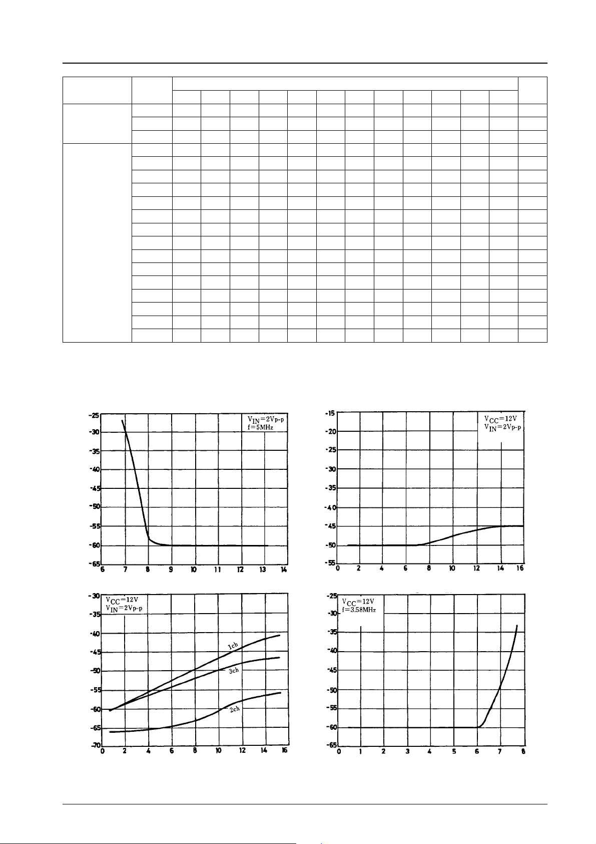
H2–V
CC
2nd harmonic – dB
Supply voltage, VCC–V
H2–f
IN
2nd harmonic – dB
Input frequency, fIN– MHz
1ch to 3ch
H
2–fIN
H
2–VIN
1ch to 3ch
2nd harmonic – dB
Input frequency, fIN– MHz
2nd harmonic – dB
Input voltage, VIN– Vp-p
No.1409-5/6
Page 6

LA7220
No products described or containedherein are intended for use in surgical implants, life-support systems, aerospace equipment,
nuclear power control systems, vehicles, disaster/crime-prevention equipment and the like, the failure of which may directly or
indirectly cause injury, death or property loss.
Anyone purchasing any products described or contained herein for an above-mentioned use shall:
1 Accept full responsibility and indemnify and defend SANYO ELECTRIC CO., LTD., its affiliates, subsidiaries and distributors
and all their officers and employees, jointly and severally, against any and all claims and litigation and all damages, cost and
expenses associated with such use:
2 Not impose any responsibility for any fault or negligence which may be cited in any such claim or litigation on SANYO
ELECTRIC CO., LTD., its affiliates, subsidiaries and distributors or any of their officers and employees jointly or severally.
Information (including circuit diagrams and circuit parameters) herein is for example only; it is not guaranteed for volume
production. SANYO believes information herein is accurate and reliable, but no guarantees are made or implied regarding its use
or any infringements of intellectual property rights or other rights of third parties.
This catalog provides information as of June, 1996. Specifications and information herein are subject to change without notice.
No.1409-6/6
 Loading...