

Page 1
Ordering number : ENA0599
Monolithic Linear IC
LA6560
For CD
Five-Channel Driver
(BTL : Four-Channel, H Bridge : One-Channel)
Overview
The LA6560 is a 5-channel driver (BTL : 4-channel, H bridge : 1-channel) for CD players.
Functions
• Power amplifier 5-channel built-in. (Bridge-connection (BTL) : 4-channel, H bridge : 1-channel)
• IO max 1A
• Level shift circuit built-in (except H bridge).
• Mute circuit (output ON/OFF) built-in.
(Operable with BTL AMP and not operable for the H bridge of 5VREG)
• 5V regulator built-in (external PNP transistor).
• With VREF changeover function (H : external, L : internal (2.5V) selected)
• Overheat protection circuit (thermal shutdown) built-in.
Specifications
Maximum Ratings at Ta = 25°C
Parameter Symbol Conditions Ratings Unit
Supply voltage V
Maximum output current IO max Each output for H bridge, channel 1 to 4. 1 A
Maximum input voltage VINB 13 V
MUTE pin voltage VMUTE 13 V
Operating temperature Topr -30 to +85 °C
Storage temperature Tstg -55 to +150 °C
* Specified board size : 76.1×114.3×1.6mm3, glass epoxy.
Recommended Operating Conditions at Ta = 25°C
Parameter Symbol Conditions Ratings Unit
Supply voltage VCC 5.6 to 13 V
max 14 V
CC
Independent IC 2.0 W Allowable power dissipation Pd max
Mounted on specified board. * 0.8 W
Any and all SANYO Semiconductor products described or contained herein do not have specifications
that can handle applications that require extremely high levels of reliability, such as life-support systems,
aircraft's control systems, or other applications whose failure can be reasonably expected to result in
serious physical and/or material damage. Consult with your SANYO Semiconductor representative
nearest you before using any SANYO Semiconductor products described or contained herein in such
applications.
SANYO Semiconductor assumes no responsibility for equipment failures that result from using products
at values that exceed, even momentarily, rated values ( such as maximum ratings, operating condition
ranges, or other parameters) listed in products specifications of any and all SANYO Semiconductor
products described or contained herein.
D0606 MS PC B8-6307 No.A0599-1/9
Page 2
LA6560
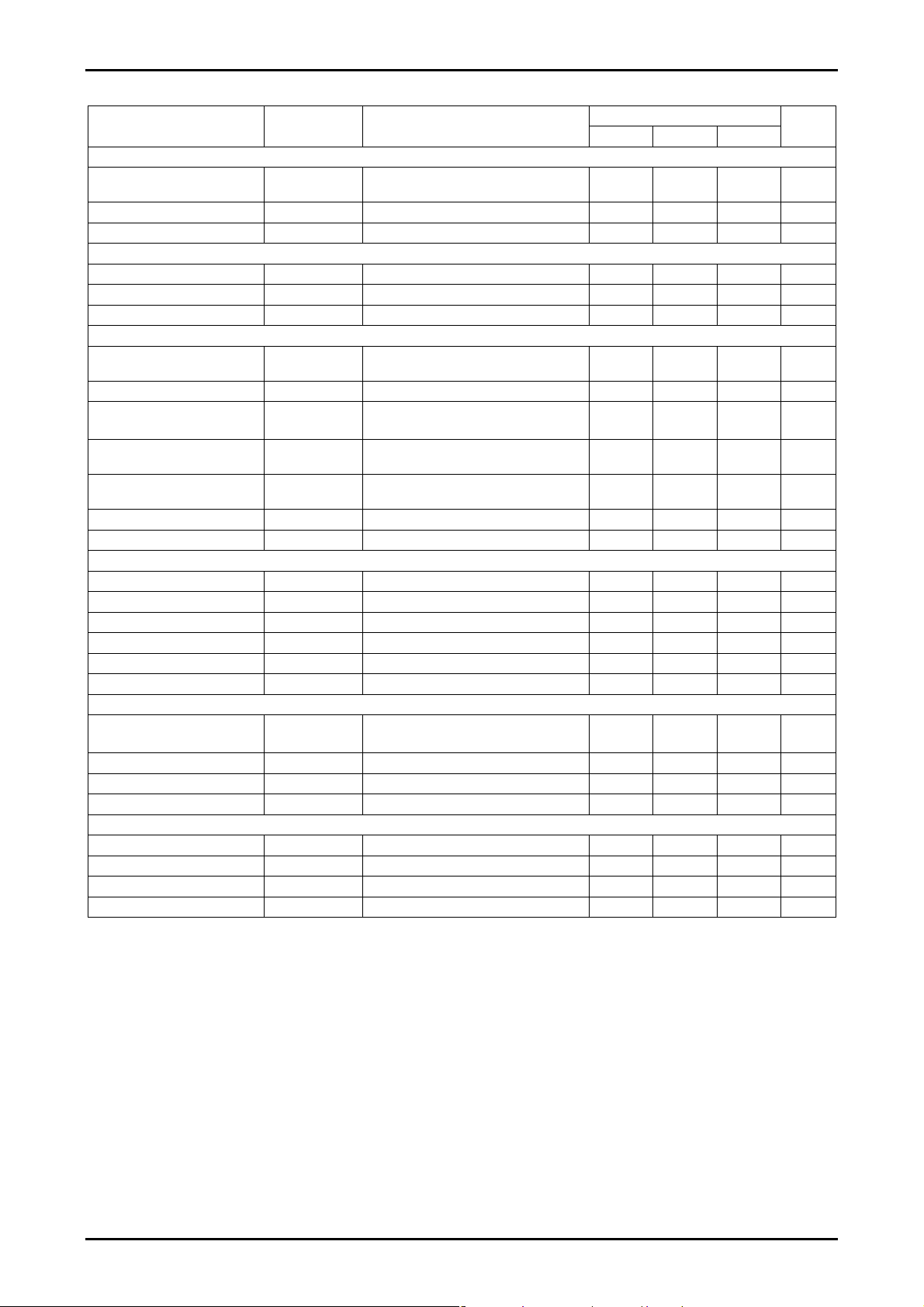
Electrical Characteristics at Ta = 25°C, VCC1 = VCC2 = 8V, VREF = 2.5V, unless especially specified.
Parameter Symbol Conditions
ALL Blocks
No-load current drain ON ICC-ON BTL-AMP output ON,
LOADING block OFF *1
No-load current drain OFF ICC-OFF
Thermal shutdown temperature TSD
VREF AMP
VREF-AMP offset voltage VREF-OFFSET
VREF Input voltage range VREF-IN
VREF-OUT output current I-VREF-OUT
BTL AMP Block (CH1 to CH4)
Output offset voltage V
Input voltage range
Output voltage VO Each voltage between V0+ and V0- when
Closed-circuit voltage gain VG Input and output gain.
Slew rate SR AMP Independent
MUTE ON voltage
MUTE OFF voltage
Input AMP Block (CH1 to 4)
Input voltage range VIN-OP
Output current (SINK) SINK-OP
Output current (SOURCE) SOURCE-OP
Output offset voltage V
CH1 input changeover voltage 1 VSW-OP1
CH1 input changeover voltage 2 VSW-OP2
Loading Block (CH5, H bridge)
Output voltage VO-LOAD At forward and reverse rotation,
Break output saturation voltage VCE-BREAK Output voltage at braking *7
Input low level VIN-L
Input high level VIN-H 2 V
Power Supply Block (PNP transistor : 2SB632K-use)
5V supply voltage V
REG-IN SINK current REG-IN-SINK Base current of external PNP *8 5 10 mA
Line regulation ΔVOLN 6V ≤ VCC ≤ 12V, IO = 200mA 10 100 mV
Load regulation ΔVOLD 5mA ≤ IO ≤ 200mA 10 100 mV
Note *1 : Current dissipatio n that is a sum of VCC1 and VCC2 at no load.
*2 : Input AMP is a BUFFER AMP.
*3 : Voltage difference between both ends of load (8Ω). Output saturated.
*4 : Output ON with MUTE : [H] and OFF with MUTE : [L] (HI impedance).
*5 : The source of input OP-AMP is a constant current. As the 11kΩ resistance to the next stage is a load, pay due attention when setting the input
OP-AMP gain.
*6 : With VIN1-SW : [L], the input AMP selects AMP-A while VREF selects internal VREF (≈ 2.5V).
With VIN1-SW : [H], the input AMP selects AMP-B while VREF selects external VREF (≈ VREF-IN).
*7 : Short (GND) brake used. SINK side output ON.
*8 : 5VREG incorporates a drooping protection circuit and operated when the base current is 10mA (TYP).
OFF
VIN Input voltage range for input for OP-AMP. 0 VCC-1.5 mA
VMUTE-ON Output ON voltage, each MUTE *4 2 V
VMUTE-OFF Output OFF voltage, each MUTE *4 0.5 V
-OP
OFF
OUT
All outputs OFF *1
Design guarantee value
-10 10 mV
1 V
CH1 input reference voltage 2 5 6.6 mA
Voltage difference between outputs for BTL
AMP, each channel. *2
RL = 8Ω. *3
Input OP-AMP:BUFFER
Multiply 2 between outputs.
0 V
2 mA
*5 300 500 μA
-10 10 mV
CH1 input AMP(B), external REF select *6 2 V
CH1 input AMP(A), internal VREF select *6 0.5 V
RL = 8Ω, VCONT=VCC *3
1V
I
= 200mA 4.8 5.0 5.2 V
O
min typ max
Ratings
30 50 mA
10 15 mA
150 175 200 °C
CC
-50 50 mV
5.7 6.2 V
3.6 4 4.4 Times
0.5 V/μs
CC
5.7 6.5 V
0.3 V
Unit
-1.5 V
-1.5 V
No.A0599-2/9
Page 3
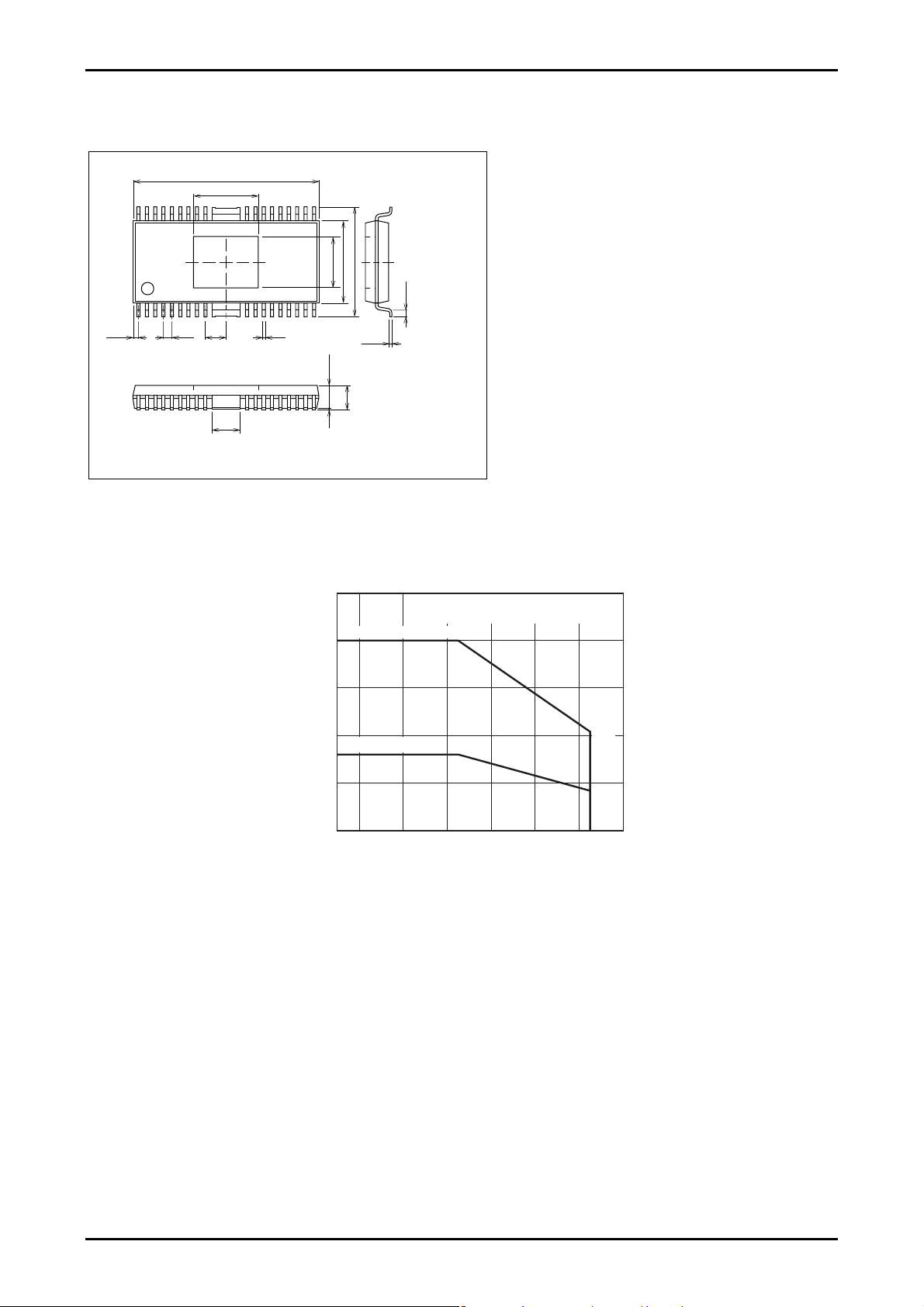
Package Dimensions
0
unit : mm (typ)
3251
0.8
17.8
(6.2)
2.0
2.7
36
(0.5)
1
19
7.9
10.5
(4.9)
0.65
18
0.3
(2.25)
0.1
0.25
2.45max
SANYO : HSOP36R(375mil)
2.5
When mounted on a board
2
1.5
1
Independent IC
0.8
0.5
Allowable power dissipation, Pd max – W
0
--30 --20 0 20 40 60
Ambient temperature, Ta – °C
LA6560
Pd max -- Ta
Specified board : 76.1×114.3×1.6mm
glass epoxy
80
3
1.04
0.42
10
No.A0599-3/9
Page 4
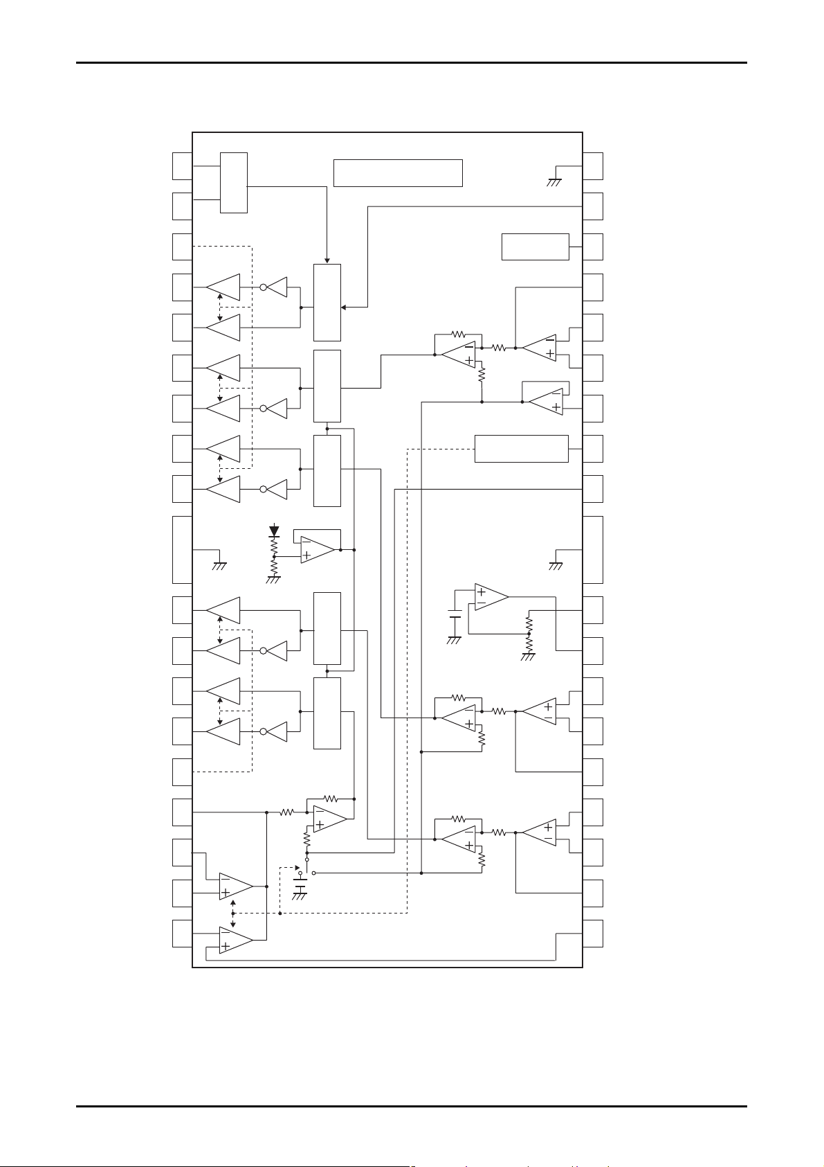
Block Diagram
FWD
REV
VCC2
VLO-
VLO+
VO4+
VO4-
VO3+
VO3-
FR
VO2+
VO2-
VO1+
VO1-
VCC1
VIN1
VIN1-A
VIN1+A
VIN1-B
1
2
3
4
5
6
7
8
9
FR
10
11
12
13
14
15
16
17
18
Input
Power system GND
11kΩ
AMP-A
AMP-B
LA6560
Thermal shutdown
Output controlLevel shiftLevel shiftLevel shiftLevel shift
22kΩ
[L] [H]
VIN1 (VREF)-SW
[L]:Internal VREF (2.5V fixed)
[H]:Internal VREF
VIN1 (VREF)-SW
[L]:AMP-A
[H]:AMP-B
Signal system GND
(LOAD output voltage setting)
BTL-AMP Output
ON/OFF
22kΩ
5VREG (Extemal PNP)
22kΩ
22kΩ
MUTE
11kΩ
VIN1/VREF-SW
Power system GND
11kΩ
11kΩ
S-GND
36
VCONT
35
MUTE
34
VIN4
33
VIN4-
32
VIN4+
31
VREF-IN
30
VIN1(VREF)-SW
29
VREF-OUT(CH1)
28
FR
FR
REG-OUT
27
REG-IN
26
VIN3+
25
VIN3-
24
VIN3
23
VIN2+
22
VIN2-
21
VIN2
20
VIN1+B
19
No.A0599-4/9
Page 5
LA6560
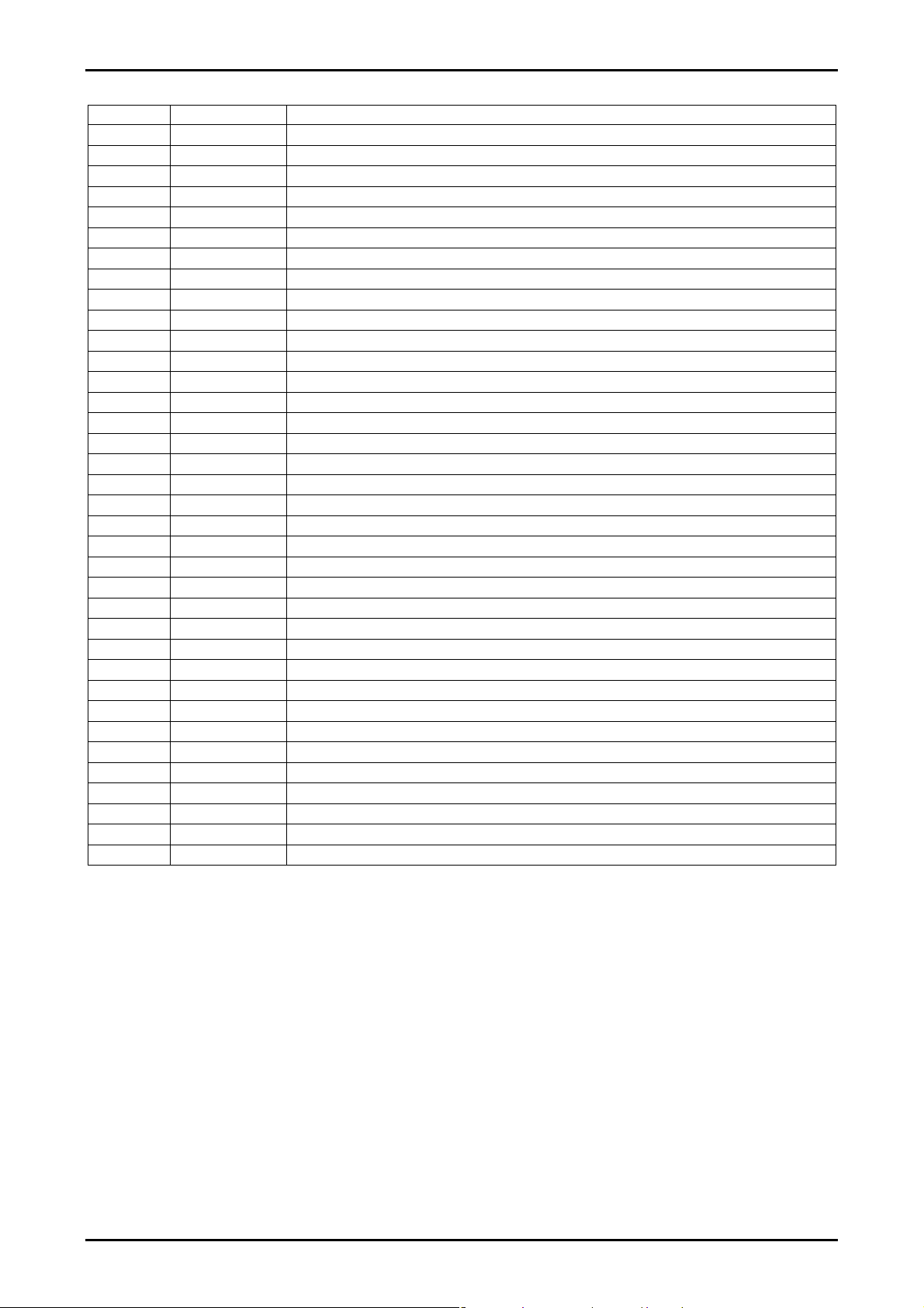
Pin Functions
Pin No. Symbol Pin descriptions
1 FWD Output change pin (FWD) for 5CH (VLO), logic input for loading block.
2 REV Output change pin (REV) for 5CH (VLO), logic input for loading block.
3 VCC2 Power supply for CH3, 4, and 5.
4 VLO- Loading output (-)
5 VLO+ Loading output (+)
6 VO4+ Output pin (+) for channel 4
7 VO4- Output pin (-) for channel 4
8 VO3+ Output pin (+) for channel 3
9 VO3- Output pin (-) for channel 3
10 VO2+ Output pin (+) for channel 2
11 VO2- Output pin (-) for channel 2
12 VO1+ Output pin (+) for channel 1
13 VO1- Output pin (-) for channel 1
14 VCC1 Power supply for CH1, 2 (BTL).
15 VIN1 Input pin for channel 1
16 VIN1-A OP-AMP input AMP-A input pin (-)
17 VIN1+A OP-AMP input AMP-A input pin (+)
18 VIN1-B Input AMP-B input pin (-) for channel 1
19 VIN1+B Input AMP-B input pin (+) for channel 1
20 VIN2 Input pin for channel 2, input AMP output
21 VIN2- Input pin (-) for channel 2
22 VIN2+ Input pin (+) for channel 2
23 VIN3 Input pin for channel 3, input AMP output
24 VIN3- Input pin (-) for channel 3
25 VIN3+ Input pin (+) for channel 3
26 REG-IN PNP transistor base connected
27 REG-OUT 5V power output to which the PNP transistor collector connected.
28 VREF-OUT CH1 reference voltage output. Outputs internal VREF (2.5V : TYP) or external VREF.
29 VIN1 (VREF) -SW Pin for changeover between input AMP-A/internal VREF (TYP2.5V) and input AMP-B/ external VREF.
30 VREF-IN Reference voltage applied pin
31 VIN4+ Input pin (+) for channel 4
32 VIN4- Input pin (-) for channel 4
33 VIN4 Input pin for channel 4, input AMP output
34 MUTE All BTL AMP output ON/OFF
35 VCONT LOADING output voltage setting
36 S-GND Signal system GND
Note : Center frame (FR) becomes GND for the power system (P-GND). Set this to the minimum potential together with S-GND.
No.A0599-5/9
Page 6
LA6560
V
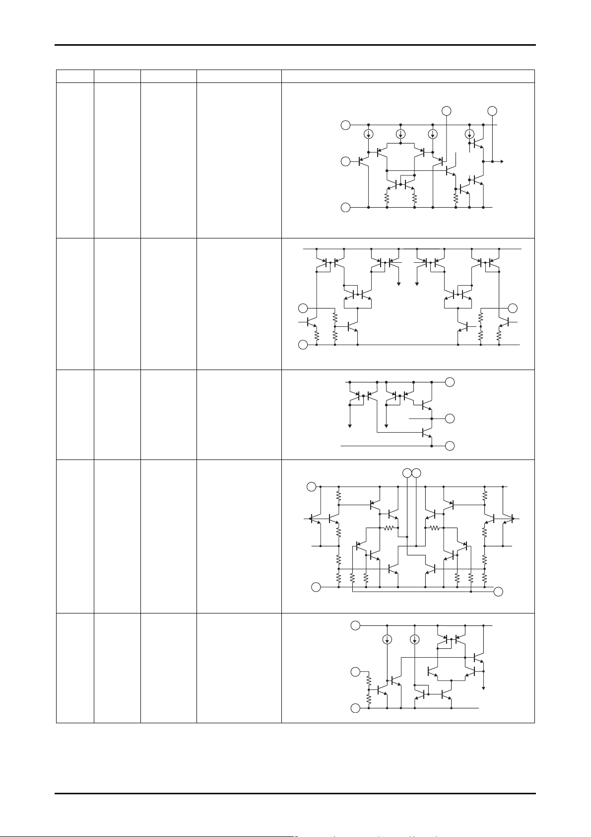
Pin Description
Pin No. Symbol Pin function Description Equivalent circuit
VIN1+A
17
VIN1+B
19
VIN1-A
16
VIN1-B
18
VIN1
15
VIN2+
22
VIN2-
21
VIN2
20
VIN3+
25
VIN3-
24
VIN3
23
VIN4-
32
VIN4+
31
VIN4
33
FWD
1
REV
2
12
VO1+
13
VO1-
10
VO2+
11
VO2-
8
VO3+
9
VO3-
6
VO4+
7
VO4VLO-
4
VLO+
5
VCONT
35
MUTE MUTE BTL AMP output, which
34
Input
(CH1 to 4)
Input
(H bridge)
Output
(BTL-AMP)
Output
(H bridge)
Input pin (CH1 to 4)
Logic input pin.
By combining H and L
of this pin, any one of
four modes (forward/
reversed/brake/idling)
can be selected.
Output for channel
1 to 4.
H bridge (LOADING)
output and LOADING
output setting pin
turns ON/OFF the
output,
MUTE : H Output OFF
MUTE : L Output OFF
FWD
S-GND
V
CC
P-GND
V
CC
VIN*+
S-GND
50kΩ
50kΩ
VLO+ VLO-
20kΩ 20kΩ1kΩ 1kΩ
VCC1
MUTE
100kΩ
100kΩ
S-GND
VIN*- VIN*
RE
50kΩ
50kΩ
VCC*
VO*
RF*
VCONT
No.A0599-6/9
Page 7
LA6560
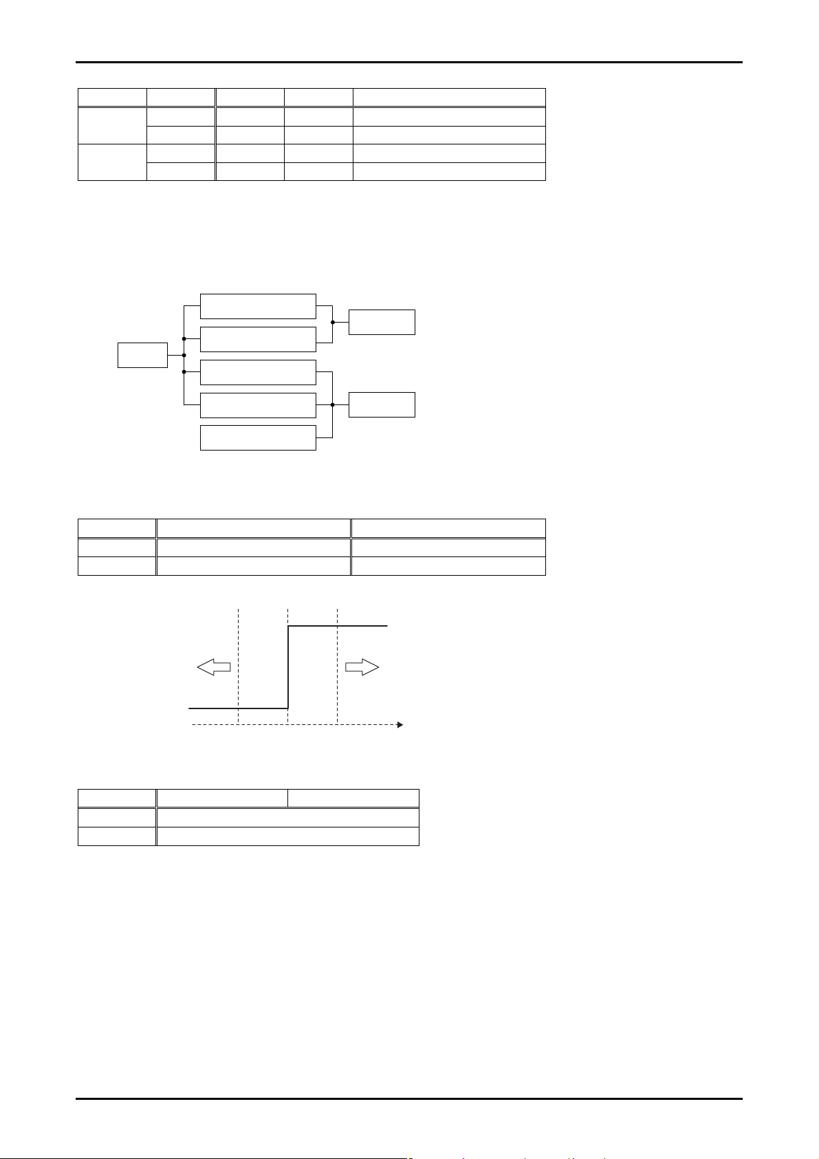
Truth Table (loading (H bridge) section)
FWD REV VLO+ VLO- Loading output
L
H
*1 The output has a high impedance.
*2 At brake, the SINK side transistor is ON (short brake).
VLO+ and VLO- are approximately on the GND level.
Relation of MUTE and Power (VCC*)
MUTE
VIN1 (VREF)-SW (CH1 input AMP selection and internal/external VREF selection function)
(Relation between input AMP (CH1 only) and VREF)
VIN1_SW Input AMP (CH1) state VREF state
H VIN1-A (AMP-A) Internal VREF (2.5V : TYP)
L VIN1-B (AMP-B) External VREF
Internal reference voltage
On MUTE
MUTE BTLAMP output VREF-OUT
L OFF
H
L OFF OFF OFF *1
H H L Forward
L L H Reversed
H L L (Short) brake *2
CH1(BTL)
VCC1
CH2(BTL)
CH3(BTL)
CH4(BTL)
CH5 (H bridge)
(2.5V (TYP))
VIN1-A VIN1-B
0.5V 2V
ON
VCC2
External reference voltage
VREF (VIN1)-SW
VREF-OUT operates in an interlock with MUTE.
No.A0599-7/9
Page 8
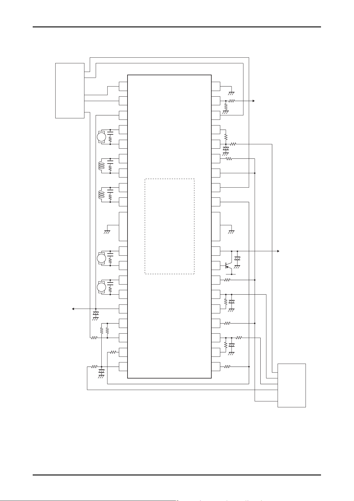
Sample Application Circuit
LOADING MOTOR
TRACKING COIL
SPINDLE MOTOR
ELEVETOR
SW
MUTE
LOADING
FOCUS COIL
SLED MOTOR
V
CC
0.1μF
M
0.1μF
0.1μF
0.1μF
M
0.1μF
M
2.2Ω
2.2Ω
2.2Ω
FR FR
10
11
2.2Ω
12
13
2.2Ω
14
15
16
17
18
1
2
3
4
5
6
7
8
9
FWD
REV
VCC2
VLO-
VLO+
VO4+
VO4-
VO3+
VO3-
FR
VO2+
VO2-
VO1+
VO1-
VCC1
VIN1
VIN1-A
VIN1+A
VIN1-B
LA6560
VIN1(VREF)-SW
VREF-OUT(CH1)
REG-OUT
S-GND
VCONT
MUTE
VIN4
VIN4-
VIN4+
VREF-IN
FR
REG-IN
VIN3+
VIN3-
VIN3
VIN2+
VIN2-
VIN2
VIN1+B
36
35
34
33
32
31
30
29
28
27
26
25
24
23
22
21
20
19
5VREG
V
CC
TRACKING
FOCUS
SPINDLE
SLED
VREF
No.A0599-8/9
Page 9
LA6560
Specifications of any and all SANYO Semiconductor products described or contained herein stipulate the
performance, characteristics, and functions of the described products in the independent state, and are
not guarantees of the performance, characteristics, and functions of the described products as mounted
in the customer's products or equipment. To verify symptoms and states that cannot be evaluated in an
independent device, the customer should always evaluate and test devices mounted in the customer's
products or equipment.
SANYO S emiconductor Co., Ltd. strives to supply high-quality high-reliability products. However, any
and all semiconductor products fail with some probability. It is possible that these probabilistic failures
could give rise to accidents or events that could endanger human lives, that could give rise to smoke or
fire, or that could cause damage to other property. Wh en designing equipment, adopt safety measures
so that these kinds of accidents or events cannot occur. Such measures include but are not limit ed to
protective ci rcuits and error prevention circuits for safe design, redundant design, and structural design.
In the event that any or all SANYO Semiconductor products (including technical data,services) described
or contained herein are controlled under any of applicable local export control laws and regulations, such
products must not be exported without obtaining the export license from the authorities concerned in
accordance with the above law.
No part of this publication may be reproduced or transmitted in any form or by any means, electronic or
mechanical, including photocopying and recording, or any information storage or retrieval system, or
otherwise, without the prior written permission of SANYO Semiconductor Co., Ltd.
Any and all information described or contained herein are subject to change without notice du e to
product/technology improvement, etc. When designing equipment, refer to the "Delivery Specification"
for the SANYO Semiconductor product that y ou intend to use.
Information (i ncluding circuit diagrams and circuit parameters) herein is for example only; it is not
guaranteed for volume production. SANYO Semiconductor believes information herein is accurate and
reliable, but no guarantees are made o r implied regarding its use or any infri ngements of intellectual
property rights or other rights of third parties.
This catalog provides information as of December, 2006. Specifications and information herein are subject
to change without notice.
PS No.A0599-9/9
Page 10

 Loading...