

Page 1

Ordering number: EN 5226
Monolithic Linear IC
LA6530M
2-channel Bridge Driver
for CD and CD-ROMs
Overview
The LA6530M is a 2-channel bridge (BTL) driver which was
developed for compact discs and CD-ROMs.
Package Dimensions
unit : mm
3073A-MFP30SLF
[LA6530M]
Features
.
High output current (IOmax = 0.7 A).
.
Wide operating voltage range (4 to 15 V).
.
Small input bias current.
SANYO : MFP30SLF
Specifications
Maximum Ratings atTa=25°C
Parameter Symbol Conditions Ratings Unit
Maximum supply voltage V
Differential input voltage V
Common-mode input voltage V
Maximum input voltage V
Mute pin maximum inflow current I
Maximum output current I
Allowable power dissipation Pd max 0.9 W
Operating temperature Topr –20 to +75
Storage temperature Tstg –55 to +150
max 16 V
CC
ID
ICM
INB
max 1.0 mA
M
max 0.7 A
O
Amplifier 2, amplifier 3 15 V
Amplifier 2, amplifier 3 15 V
Buffer amplifier 15 V
C
°
C
°
Operating Conditions atTa=25°C
Parameter Symbol Conditions Ratings Unit
Recommended supply voltage V
Operating voltage range V
Recommended load resistance R
CC
CC
op 4.0 to 15.0 V
L
Pin 11 to 20, pin 5 to 26 8.0 Ω
5.0 V
SANYO Electric Co.,Ltd. Semiconductor Bussiness Headquarters
TOKYO OFFICE Tokyo Bldg., 1-10, 1 Chome, Ueno, Taito-ku, TOKYO, 110 JAPAN
92995HA(II) No.5226-1/4
Page 2

LA6530M
Electrical Characteristics atTa=25°C, VCC= 5.0 V
Parameter Symbol
I
No-load current drain
I
I
I
Output offset voltage
V
V
Input-output voltage difference V
Input voltage range V
Common-mode input voltage
range
V
Input bias current I
Output voltage V
Bridge output voltage difference V
1 Mute off pins 7, 22 and 24 connected to GND 5 10 20 mA
CC
2 Mute on pins 7, 22 and 24 connected to GND 3 7 15 mA
CC
3 Mute off pins 7, 22 and 24 connected to 1/2 V
CC
4 Mute on pins 7, 22 and 24 connected to 1/2 V
CC
1 OUT1-OUT2 –50 +50 mV
OF
2 OUT4-OUT3 –50 +50 mV
OF
BIO
BICM
ICM
B
OD
Buffer amplifier –30 +30 mV
Buffer amplifier 1.5 VCC−1.5 V
Amplifier 2, amplifier 3 1.0 VCC−1.5 V
8 Ω load between pins 11 — 20,5—26 2.8 3.3 V
O
8 Ω load between pins 11 — 20,5—26 1.8 2.2 V
Conditions
CC
CC
min typ max Unit
10 20 30 mA
4 8 16 mA
50 300 nA
Closed-circuit voltage gain VG Specified Test Circuit,f=1kHz 30 38 dB
Mute on voltage V
Mute pin inflow current I
M
M
0.7 V
3.0 µA
*Thermal shutdown function built in.
Notes:
1. When the muting function is on, the OUT1 to OUT4 outputs are turned off and the buffer output is not turned off.
2. This IC must be handled carefully owing to its susceptibility electrostatic discharge damage.
Pd max — Ta
Allowable power dissipation, Pd max — W
Ambient temperature, Ta —°C
No.5226-2/4
Page 3
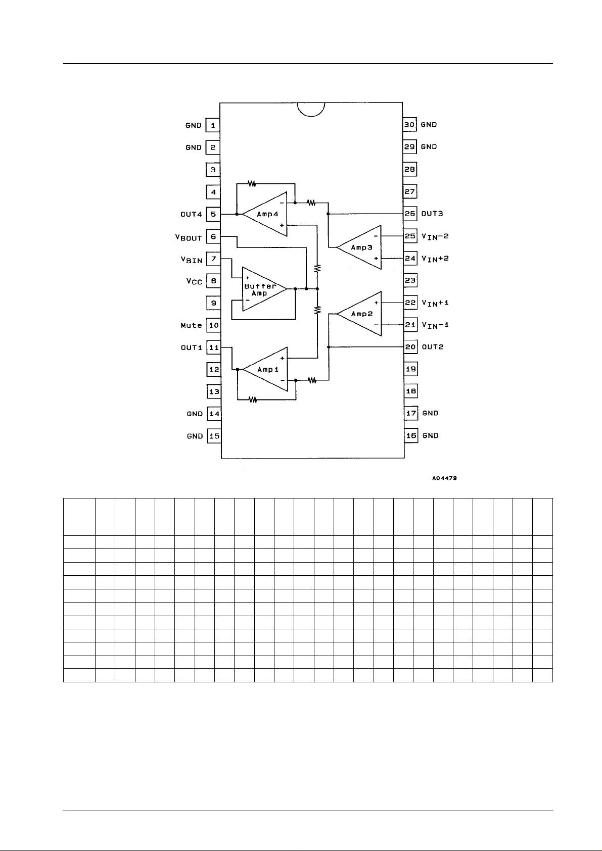
Block Diagram and Pin Assignment
LA6530M
Do not use the NC pin.
(NC)
(NC)
(NC)
(NC)
(NC)
(NC)
(NC)
(NC)
(NC)
(NC)
Top view
Test Method
SW
No.
1234567891011121314151617181920212223
Item
a b OFF OFF OFF OFF b OFF OFF OFF b b a OFF a OFF OFF OFF OFF OFF OFF a b
1
I
CC
a c OFF OFF OFF OFF b OFF OFF OFF b b a OFF a OFF OFF OFF OFF OFF OFF a b
2
I
CC
a b OFF OFF OFF OFF b OFF OFF OFF b c a OFF a OFF OFF OFF OFF OFF OFF b b
3
I
CC
a c OFF OFF OFF OFF b OFF OFF OFF b c a OFF a OFF OFF OFF OFF OFF OFF b b
4
I
CC
b b OFF OFF OFF ON b OFF OFF OFF b c a OFF a OFF OFF ON OFF OFF OFF b b
1,2
V
OF
V
BIO
I
B
V
O
V
OD
VG b b ON OFF OFF OFF a ON OFF ON b c a ON b ON OFF OFF OFF ON OFF b b
V
M
1. For ICC1 to 4, measure the circuit current.
2. For V
3. For V
4. For I
5. For V
6. For V
7. For VG, measure the voltage on pins 11, 20, 5 and 26 atf=1kHz, and use the following formula:
8. V
b b OFF OFF OFF ON b OFF OFF OFF b c a OFF a OFF OFF ON OFF OFF OFF b b
b b OFF OFF OFF OFF a OFF OFF OFF a c b OFF b OFF OFF OFF OFF OFF OFF b a
b b OFF ON ON OFF b OFF ON OFF b a a OFF a OFF ON OFF ON OFF ON b b
b b OFF OFF ON ON b OFF OFF OFF b a a OFF a OFF OFF ON ON OFF OFF b b
b a OFF ON OFF OFF b OFF ON OFF b c a OFF a OFF ON OFF OFF OFF ON b b
1 and 2, measure the voltage between pins 11 and 20 and the voltage between pins 5 and 26.
OF
, measure the voltage between pins 7 and 6.
BIO
, measure the voltage across the 100 kΩ resistor.
B
, measure the voltage on pins 11, 20, 5 and 26 by switching the input pin voltage to 0.5 V and 4.5 V, respectively.
O
, measure the voltage between pins 11 and 20 and the voltage between pins 5 and 26.
OD
VG = 20 log V
is the mute voltage when the mute voltage is varied and the output is turned off.
M
O/V1
dB.
No.5226-3/4
Page 4
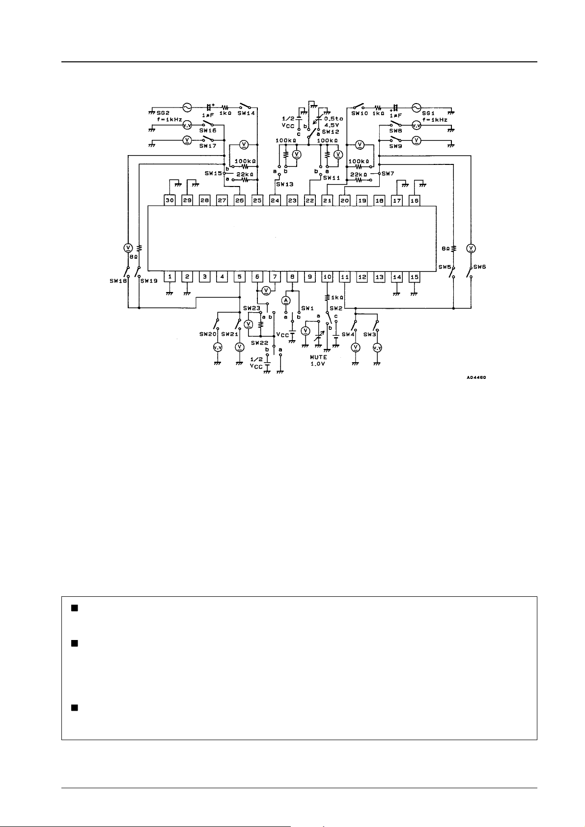
Test Circuit
LA6530M
No products described or contained herein are intended for use in surgical implants, life-support systems, aerospace equipment,
nuclear power control systems, vehicles, disaster/crime-prevention equipment and the like, the failure of which may directly or
indirectly cause injury, death or property loss.
Anyone purchasing any products described or contained herein for an above-mentioned use shall:
1 Accept full responsibility and indemnify and defend SANYO ELECTRIC CO., LTD., its affiliates, subsidiaries and distributors
and all their officers and employees, jointly and severally, against any and all claims and litigation and all damages, cost and
expenses associated with such use:
2 Not impose any responsibility for any fault or negligence which may be cited in any such claim or litigation on SANYO
ELECTRIC CO., LTD., its affiliates, subsidiaries and distributors or any of their officers and employees jointly or severally.
Information (including circuit diagrams and circuit parameters) herein is for example only; it is not guaranteed for volume
production. SANYO believes information hereinisaccurate and reliable, but no guarantees are made or implied regarding its use
or any infringements of intellectual property rights or other rights of third parties.
This catalog provides information as of September, 1995. Specifications and information herein are subject to change without notice.
No.5226-4/4
 Loading...