

Page 1
Overview
The LA6503 was developed for CAV control CD-ROM
drives, and provides spindle motor driver, sled motor
driver, and sled motion/position detection circuits.
Functions and Features
• CAV control spindle motor driver
— Three-phase brushless motor driver
—IOmax = 1 A
— Built-in FG output circuit (single Hall detection
output)
— Reverse braking circuit
— Built-in start/stop circuit
— Upper side current detection for minimal loss in the
current detection resistor. Also, the voltage drop in
this resistor reduces the IC internal power
dissipation.
— Built-in thermal shutdown circuit
• Sled motor driver
— One built-in BTL driver channel
—IOmax = 1 A
— Wide dynamic range
— Built-in level shifting circuit
— Muting (output on/off) circuit
— Built-in thermal shutdown circuit
• Sled motion/position detection circuit
— Circuit that provides a pulse output corresponding to
sled motion and position
— This circuit emits 96 pulses for each rotation from
a 24-pole magnet and 90° phase difference Hall
element motors, and thus detects the distance
moved. It also provides two 48-pulse outputs with
differing phases such that the motion direction can
be detected from the phase difference between those
signals.
• Hall bias power supply
— Generates the Hall element 3-V bias voltage.
—IOmax = 30 mA, typical
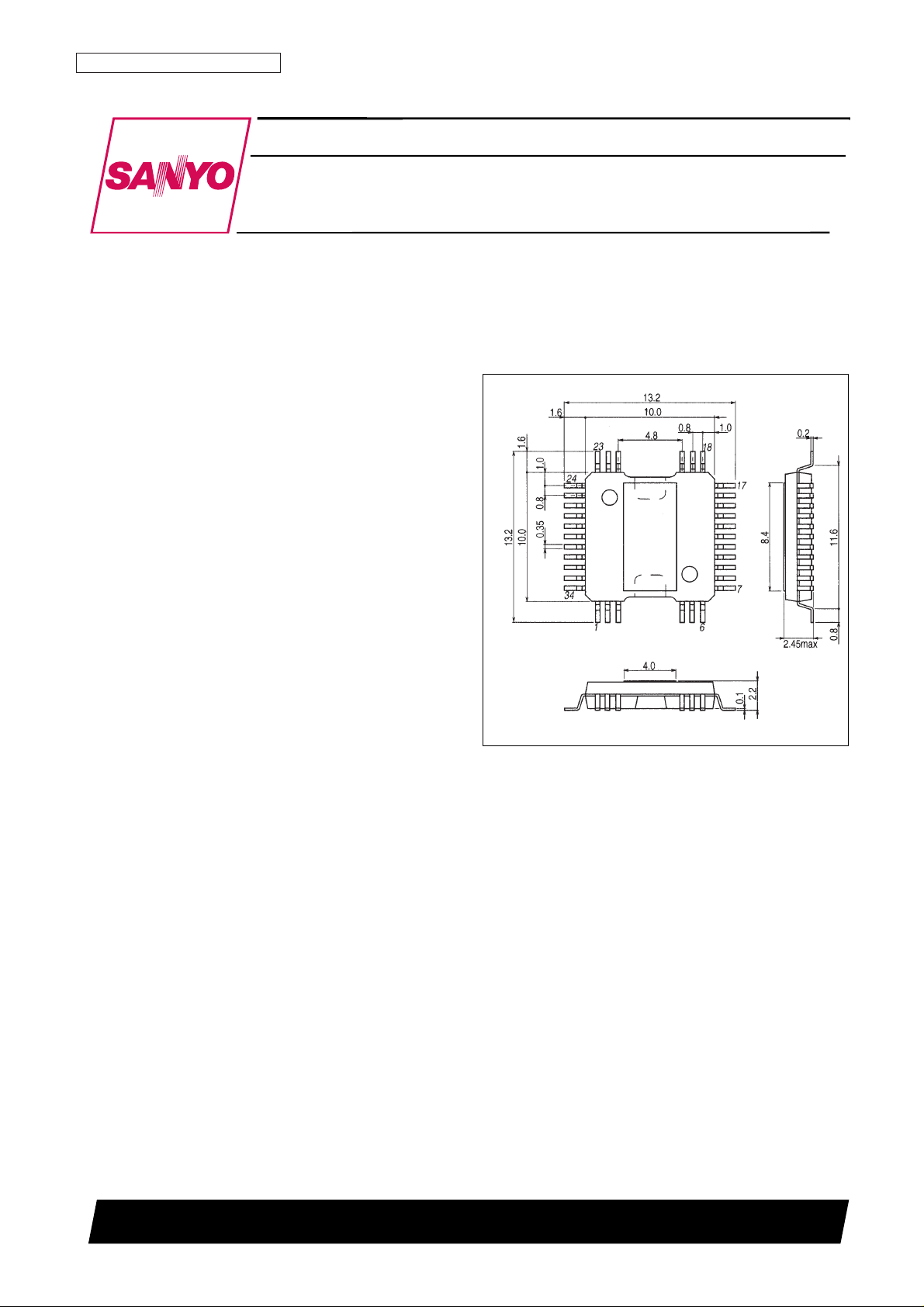
Package Dimensions
unit: mm
3219-QFP34H-C
Monolithic Linear IC
31398HA (OT) No. 5791-1/8
SANYO: QFP34H-C
[LA6503]
SANYO Electric Co.,Ltd. Semiconductor Bussiness Headquarters
TOKYO OFFICE Tokyo Bldg., 1-10, 1 Chome, Ueno, Taito-ku, TOKYO, 110-8534 JAPAN
CD-ROM Drive Spindle Motor Driver + Sled Motor
Driver + Sled Motion/Position Detector IC
LA6503
Ordering number : EN5791
Page 2
No. 5791-2/8
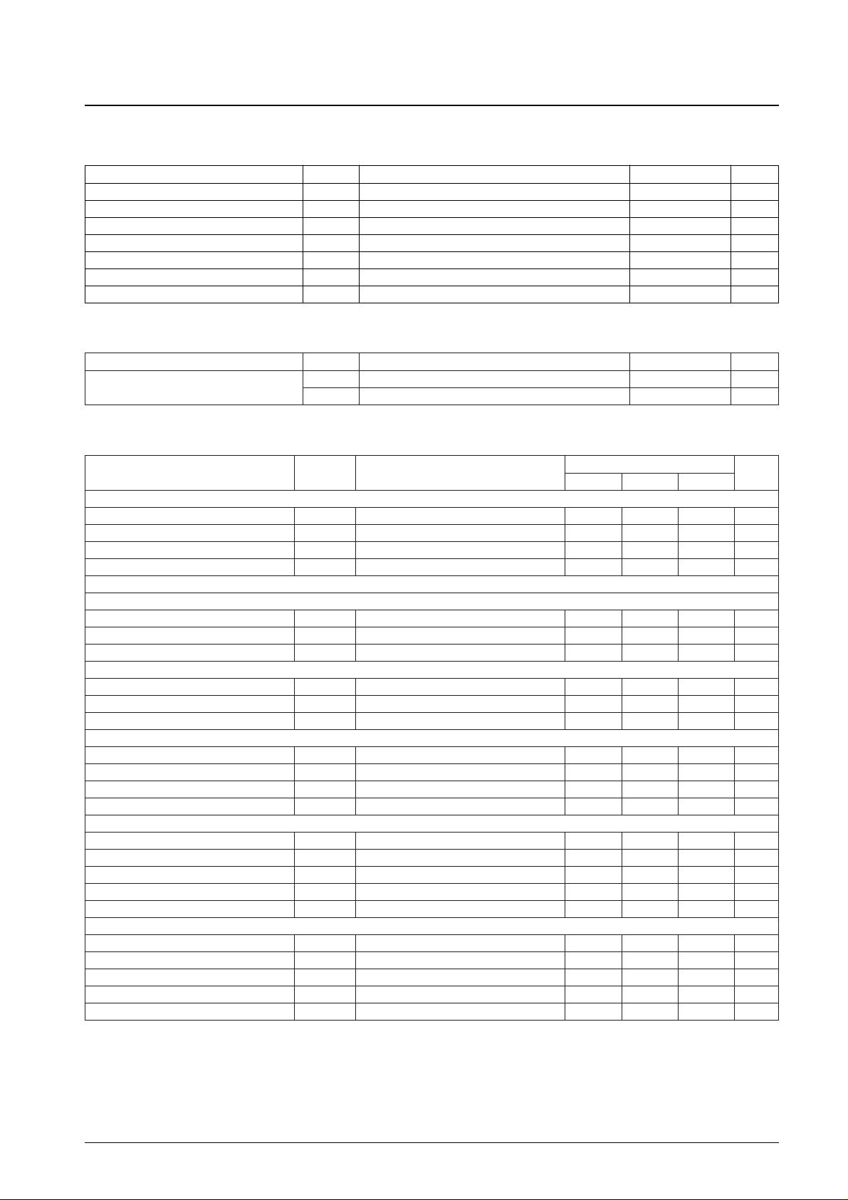
LA6503
Parameter Symbol Conditions Ratings Unit
Supply voltage V
CC
max 7 V
Supply voltage V
M
max 14 V
Input voltage V
C
max V
CC
V
Output current I
O
max Spindle output, sled output 1 A
Allowable power dissipation Pd max Independent IC 0.77 W
Operating temperature Topr –20 to +75 °C
Storage temperature Tstg –55 to +150 °C
Specifications
Maximum Ratings at Ta = 25°C
Parameter Symbol Conditions
Ratings
Unit
min typ max
[Power Supply Current]
Current drain 1 (V
CC
) ICC1 START/STOP = MUTE = 5 V 10 20 mA
Current drain 2 (V
M
) IM1 START/STOP = MUTE = 5 V 25 50 mA
Quiescent current 1 (V
CC
) ICC2 START/STOP = MUTE = 0 V 5 10 mA
Quiescent current 2 (V
M
) IM2 START/STOP = MUTE = 0 V 1 5 mA
[Spindle Motor Block]
[Output]
Upper side saturation voltage 1 V
sourceIO
= –0.5 A 1.0 1.5 V
Lower side saturation voltage 1 V
sinkIO
= +0.5 A 0.33 0.80 V
Current limiter voltage setting V
CL
RRE= 0.43 Ω 0.32 V
[Hall Amplifier]
Common-mode input voltage range V
HCOM
1.2 VCC– 1.0 V
Input bias current V
HIB
1 µA
Minimum Hall input level V
HIN
60 mVp-p
[S/S Pin]
High-level voltage VS/SH 2.0 V
CC
V
Low-level voltage VS/SL 0.7 V
Input current IS/SI VS/S = 5 V 200 µA
Leakage current IS/SL VS/S = 0 V –30 µA
[Control]
VC pin input current I
VC
VC= V
CREF
= 2.5 V 1 5 µA
VCREF pin input current I
VCREFVC
= V
CREF
= 2.5 V 1 5 µA
Voltage gain G
VCO
∆VRF/∆V
C
0.25 Times
Rising edge threshold voltage V
CTH
V
CREF
= 2.5 V 2.35 2.65 V
Rising edge threshold voltage difference ∆V
CTHVCREF
= 2.5 V 50 150 mV
[Hall Comparator]
Input offset voltage V
HCIOFFSET
10 mV
Input hysteresis V
HCIHYS
8 mV
Output on voltage V
OU
0.3 V
Output off voltage V
OD
* 4.7 V
Output current (sink) I
sink
3 mA
Operating Characteristics at Ta = 25°C, VCC= 5 V, VM= 12 V (unless otherwise specified)
Parameter Symbol Conditions Ratings Unit
Operating supply voltage range
V
CC
4.6 to 6.0 V
V
M
4.6 to 13.0 V
Operating Conditions at Ta = 25°C
Continued on next page.
Page 3
No. 5791-3/8
LA6503
Continued from preceding page.
Parameter Symbol Conditions
Ratings
Unit
min typ max
[Sled Motor Block]
Output offset voltage V
OFF
Voltage difference between outputs –50 +50 mV
Buffer input voltage range V
BIN
1.5 VCC– 1.5 V
Input voltage range V
IN
1.0 VCC– 1.5 V
Source output voltage V
O
1 RL= 8 Ω 9.5 10.1 V
Sink output voltage V
O
2 RL= 8 Ω 1.8 2.4 V
Closed-circuit voltage gain VG Bridge Amp 12 dB
Slew rate S
R
0.15 V/µs
Muting on voltage V
MUTE
The amplifier output is on when at the high level. 0.7 1.2 2.0 V
[Hall Bias (3-V Output Power Supply)]
Output voltage V
HB-OUTIOUT
= 30 mA 2.5 3.0 3.5 V
Line regulation V
HB-LINVCC
= 4.6 to 6 V, I
OUT
= 30 mA –50 +50 mV
Load regulation V
HB-LOADIOUT
= 5 to 30 mA, VCC= 5 V –200 +200 mV
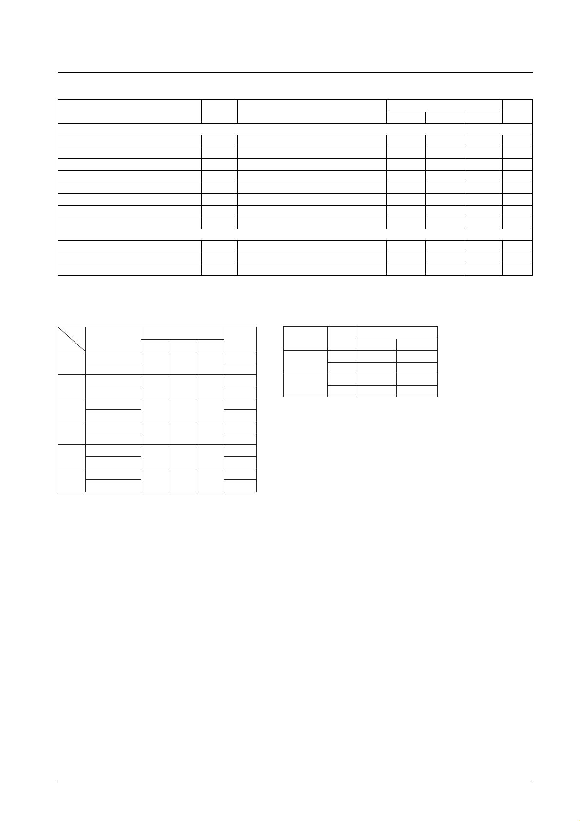
Truth Table
(Spindle Motor Block)
Inputs: The “H” state is when the + input of the corresponding
phase is 0.2 V or more higher than the – input.
The “L” state is when the + input of the corresponding
phase is 0.2 V or more lower than the – input.
Note: For items marked with an asterisk (*), the Hall comparator goes to the high level when the S/S pin is off (standby mode).
Source
→ Sink
Input Control
U V W VC
1
W → V
H H L
H
V → W L
2
W → U
H L L
H
U → W L
3
V → W
L L H
H
W → V L
4
U → V
L H L
H
V → U L
5
V → U
H L H
H
U → V L
6
U → W
L H H
H
W → U L
(Sled Motor Block)
Note: “—” indicates that the amplifier output is off.
Input (V
IN
) Mute
Output
SLD-OUT+ SLD-OUT–
H
H H L
L — —
L
H L H
L — —
Page 4
No. 5791-4/8
LA6503
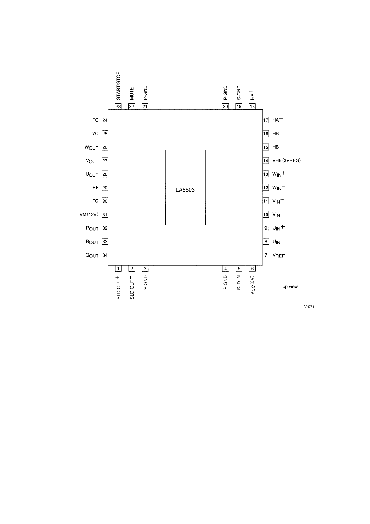
Pin Assignment
Page 5
No. 5791-5/8
LA6503
Pin Functions
Pin No. Symbol Function
1 SLED OUT
+
Sled motor noninverted output
2 SLED OUT
–
Sled motor inverted output
3 P-GND Power system ground
4 P-GND Power system ground
5 SLED-IN Sled motor signal input (The gain is set with a resistor.)
6 V
CC
(5 V) Signal system power supply (5 V)
7 V
REF
Reference voltage input
8 U
IN
–
Three-phase spindle motor hall signal input pin (U phase –)
9 U
IN
+
Three-phase spindle motor hall signal input pin (U phase +)
10 V
IN
–
Three-phase spindle motor hall signal input pin (V phase –)
11 V
IN
+
Three-phase spindle motor hall signal input pin (V phase +)
12 W
IN
–
Three-phase spindle motor hall signal input pin (W phase –)
13 W
IN
+
Three-phase spindle motor hall signal input pin (W phase +)
14 VHB (3Vreg) Hall bias output pin (3-V power supply output)
15 HB
–
Sled motion distance detection hall element input (HB –)
16 HB
+
Sled motion distance detection hall element input (HB +)
17 HA
–
Sled motion distance detection hall element input (HA –)
18 HA
+
Sled motion distance detection hall element input (HA +)
19 S-GND Signal system ground
20 P-GND Power system ground
21 P-GND Power system ground
22 MUTE Sled motor output muting (output on/off control)
23 START/STOP Spindle motor output start/stop (output on/off control)
24 FC Phase compensation capacitor connection
25 VC Input for the spindle control signal from the ASP
26 WOUT Three-phase spindle motor output (W phase output)
27 VOUT Three-phase spindle motor output (V phase output)
28 UOUT Three-phase spindle motor output (U phase output)
29 RF Output current detection
30 FG FG signal output
31 V
M
(12 V) Motor power supply (12 V)
32 POUT Sled motion position detection pulse output P (96 pulses)
33 ROUT Sled motion position detection pulse output R (48 pulses)
34 QOUT Sled motion position detection pulse output Q (48 pulses)
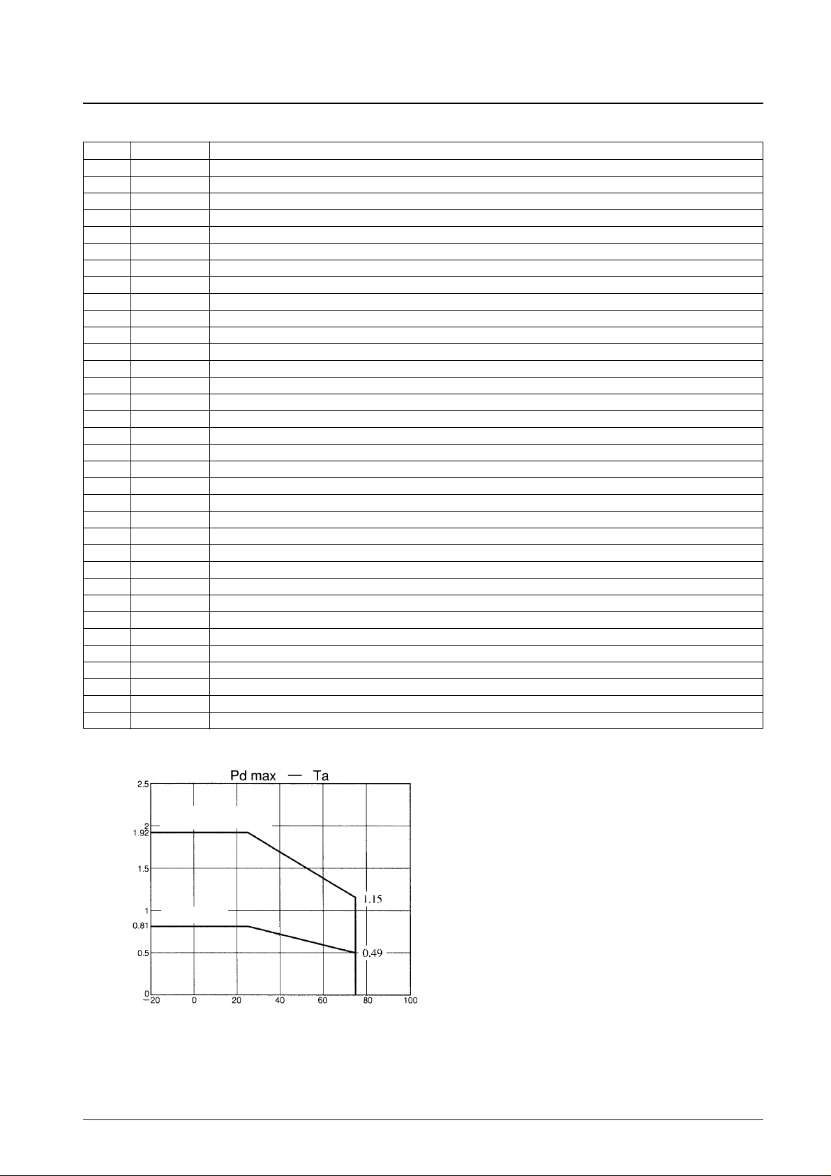
Ambient temperature, Ta – ˚C
Allowable power dissipation, Pdmax – W
Mounted on the specified
printed circuit board
Independent IC
Page 6
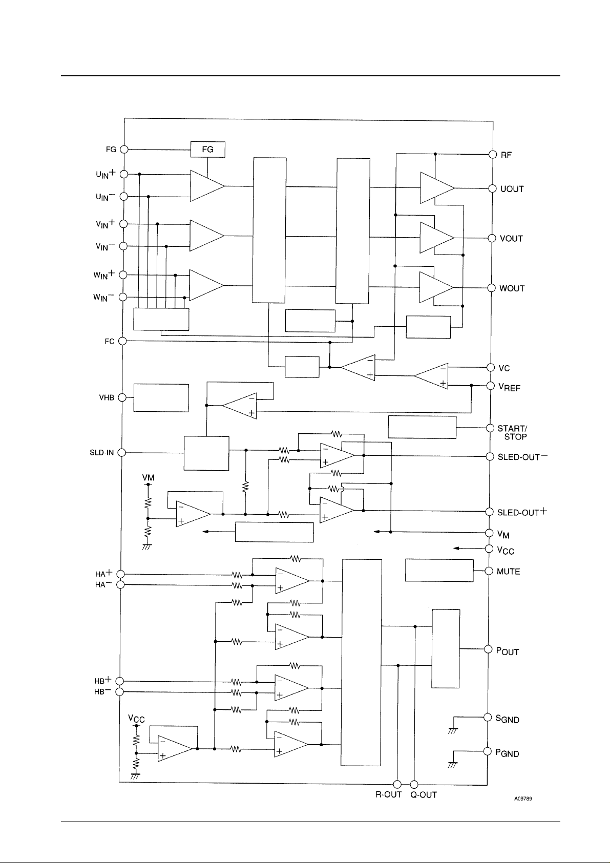
Block Diagram
No. 5791-6/8
LA6503
Reverse rotation
detection
Matrix
Pulse generator circuit
Pulse generator circuit
Control circuit
Hall bias
(3-V regulator)
Current limiter
Reverse
braking
Start/stop
(Spindle motor on/off)
Muting
(Sled motor on/off)
Forward/
reverse
Level
shifter
To each bias circuit
Power system ground
Thermal shutdown
circuit
Page 7

Notes on Gain Adjustment (Sled Motor Block)
• Gain setting
The sled motor block gain is set using an external resistor as shown below.
For example, when the external resistor R is 22 kΩ, the gain will be 0 dB when seen as an independent output amplifier
and 6 dB when seen as a BTL circuit (between outputs). Referenced to this 22-kΩ resistor, the independent output
amplifier gain will be 22k/R (as a multiple) or 20 log(22k/R) dB. Similarly, the BTL gain will be 2×22k/R
(as a multiple) or 20 log(22k/R) dB + 3 dB. The level shifting circuits used in current models perform both current and
voltage conversion, and thus have a different input type from normal operational amplifiers. The current that flows in
the external resistor, that is, the potential difference, becomes the input to AMP1 and AMP2.
• Output offset voltage
The output offset voltage is 1/2 VM(typical). The V
O
–
and V
O
+
outputs are converted to outputs that are centered on
this voltage.
No. 5791-7/8
LA6503
(Input)
Resistor R
Page 8
PS No. 5791-8/8
LA6503
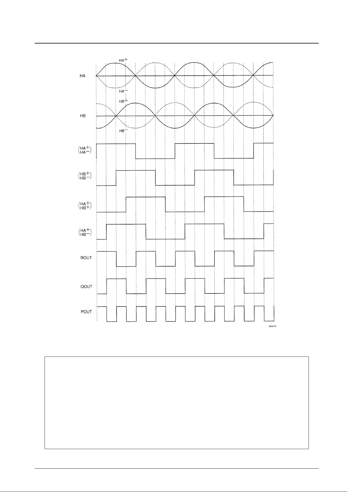
Note: When the sled motor rotation direction changes (that is, when the HA and HB phase relationship changes), the R-OUT and Q-OUT phase relationship
changes and the direction can be detected from that phase. The motion distance and position are detected from P-OUT.
This catalog provides information as of March, 1998. Specifications and information herein are subject to
change without notice.
■ No products described or contained herein are intended for use in surgical implants, life-support systems, aerospace
equipment, nuclear power control systems, vehicles, disaster/crime-prevention equipment and the like, the failure of
which may directly or indirectly cause injury, death or property loss.
■ Anyone purchasing any products described or contained herein for an above-mentioned use shall:
➀ Accept full responsibility and indemnify and defend SANYO ELECTRIC CO., LTD., its affiliates, subsidiaries and
distributors and all their officers and employees, jointly and severally, against any and all claims and litigation and all
damages, cost and expenses associated with such use:
➁ Not impose any responsibility for any fault or negligence which may be cited in any such claim or litigation on
SANYO ELECTRIC CO., LTD., its affiliates, subsidiaries and distributors or any of their officers and employees
jointly or severally.
■ Information (including circuit diagrams and circuit parameters) herein is for example only; it is not guaranteed for
volume production. SANYO believes information herein is accurate and reliable, but no guarantees are made or implied
regarding its use or any infringements of intellectual property rights or other rights of third parties.
Sled Position Detection Pulse Waveforms
 Loading...