


www.fairchildsemi.com
FAN5233
System Electronics Regulator for Mobile PCs
Features
• 5.4V to 24V input voltage range
• Five regulated outputs:
• 5V @ 5A (PWM)
• 3.3V @ 5A (PWM)
• 5V @ 50mA Always On (Linear)
• 12V/Adjustable @ 120mA Boost (PWM)
• >96% efficiency
• Hysteretic mode for light loads
• PWM mode for normal loads
• Main regulators switch out of phase
• 300kHz fixed frequency switching
• RDS(ON) current sense over-current
• Reduced BOM; Max. efficiency
• Optional current sense resistor for precision over-current
detect
• Power Good signal for all voltages
• Input under-voltage lock-out (UVLO)
• Thermal shutdown
• ACPI compliant
• 24-pin TSSOP
Applications
• Notebook PCs
• Web tablets
• Battery-powered instruments
Description
The FAN5233 is a high efficiency and high precision
multiple-output voltage regulator for notebook PC and other
similar battery-powered applications. It integrates three
pulse-width modulated (PWM) switching regulator
controllers and one linear regulator to convert 5.4V-to-24V
notebook battery power into the voltage used by the circuitry
that surrounds the microprocessor in these systems.
The two primary PWM controllers in the FAN5233 use
synchronous-mode rectification to provide 3.3V and 5V at
over 5A each. They switch out-of-phase to minimize input
ripple-current. Utilization of both input and output voltage
feedback in a current-mode control allows for fast and stable
loop response over a wide range of input and output
variations. PWM control in normal operation and hysteretic
control under light load provides efficiency of greater than
95% over a wide range of input and output variations. The
third PWM controller generates 12V at 120mA. A proprietary technology is used for sensing of output current using
the RDS(ON) of the external MOSFETs, eliminating external current sense resistors which saves board space and
reduces BOM cost.
One integrated linear regulator provides stand-by
ALWAYS-ON power at 5V for light (50mA) loads.
Additional FAN5233 features include over-voltage, undervoltage, and over-current monitors and thermal shutdown
protection. A single Power-Good signal is issued when soft
start is completed and all outputs are within ±10% of their
settings.
REV. 1.0.6 1/22/02
2
FAN5233 PRODUCT SPECIFICATION
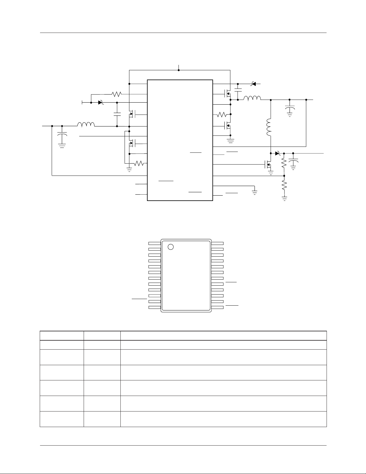
Typical Application
Vin = 5.4-24V
FAN5233
5V-ALWAYS
5V @ 5A
+
5V-ALWAYS
1 VIN
2 FPWM
3 CPUMP3.3
CPUMP5 24
HSD5 23
SW5 22
3.3V @ 5A
+
Pin Assignments
5V-ALWAYS@ 50mA
PGOOD
SDN3.3
CPUMP3.3
HSD3.3
5V-ALWAYS
GND3.3
ISEN3.3
PGOOD
VIN
FPWM
SW3.3
LSD3.3
VFB3.3
SDN3.3
4 HSD3.3
5 SW3.3
6 5V-ALW
7 LSD3.3
8 GND3.3
9 ISEN3.3
10 VFB3.3
11 SDN3.3
12 PGOOD
1
2
3
4
5
6
7
8
9
10
11
12
ISEN5 21
LSD5 20
GND5 19
VFB5 18
SDN5 17
SW12 16
VFB12 15
SGND 14
SDWN 13
Top View
24
23
22
21
20
19
18
17
16
15
14
13
SDN5
VFB12
SDWN
CPUMP5
HSD5
SW5
ISEN5
LSD5
GND5
VFB5
SDN5
SW12
VFB12
SGND
SDWN
12V @ 120mA
+
Pin Description
Pin Name Pin Number Pin Function Description
VIN 1
FPWM 2
CPUMP3.3 3
HSD3.3 4
SW3.3 5
5V-ALWAYS 6
Input power.
Mode Control. Taking this pin to +5V forces PWM mode of operation. Pull to
GND for normal operation. During Start-up FPWM pin should be forced high.
Charge Pump 3.3V. High side Gate drive voltage for 3.3V. This pin is to be
connected to SW3.3 through a 100nF cap. and to 5V-ALWAYS through a diode
High-side gate driver for 3.3V. Connect this pin directly to the gate of an
N-channel MOSFET. The trace from this pin to the MOSFET gate should be < 1".
High side FET Source and Low Side FET Drain Switching Node. Switching
node for 3.3V.
5V Always on linear regulator output. This pin should be decoupled to ground
with a 10µF capacitor.
REV. 1.0.6 1/22/02
PRODUCT SPECIFICATION FAN5233
Pin Description
Pin Name Pin Number Pin Function Description
LSD3.3 7
GND3.3 8
ISEN3.3 9
VFB3.3 10
SDN3.3 11
PGOOD 12
SDWN 13
SGND 14
VFB12 15
SW12 16
SDN5 17
VFB5 18
GND5 19
LSD5 20
ISEN5 21
SW5 22
HSD5 23
CPUMP5 24
(Continued)
Low-side gate driver for 3.3V. Connect this pin directly to the gate of an
N-channel MOSFET. The trace from this pin to the MOSFET gate should be < 1".
Ground for 3.3V MOSFET.
Current sense for 3.3V. This pin should be connected to the Drain of the bottom
Mosfet with an appropriate resistor and an RC filter. See Application Section.
Voltage feedback for 3.3V.
Soft Start and ON/OFF for 3.3V. OFF=GND. ON=open with SDWN=High. Use
open collector device for control.
Power Good Flag. An open collector output that will be logic low if any output
voltage is not above 89% of the nominal output voltage.
Master Shutdown. Shutdown for all power. Off when low. When high
5V/3.3V-ALWAYS are ON while 5V/3.3V-Main are ready to turn on if SDN5,
SDN3.3 go open.
Signal ground.
Voltage feedback for 12V.
FET driver for 12V Boost.
Enable/Soft Start for 5V and 12V. Soft start and ON/OFF for 5V & 12V.
OFF=Grounded. ON=open with SDWN
Voltage feedback for 5V.
Ground for 5V MOSFET.
Low side FET driver for 5V. Connect this pin directly to the gate of an N-channel
MOSFET. The trace from this pin to the MOSFET gate should be < 1".
Current Sense for 5V. This pin should be connected to the drain of the bottom
Mosfet using appropriate resistor and RC filter. See Application Section.
High Side Driver Source and Low Side Driver Drain Switching Node.
Switching node for 5V.
High side FET driver for 5V. Connect this pin directly to the gate of an N-channel
MOSFET. The trace from this pin to the MOSFET gate should be < 1".
Charge Pump 5V. High side Gate drive voltage for 5V. High side Gate drive
voltage for 5V. This pin is to be connected to SW5 through a 100nF cap. and to
5V-ALWAYS through a diode.
=High.
REV. 1.0.6 1/22/02
3
4
Ω
Ω
FAN5233 PRODUCT SPECIFICATION
Absolute Maximum Ratings
Parameter Conditions Min. Typ. Max. Units
V
IN
SW, ISEN Pins,SDWN Pin -0.3 27 V
CPUMP, HSD Pins -0.3 33 V
SDN, VFB, V_always pins -0.3 6.5 V
CPUMP to SW pins, and all other pins -0.3 6.5 V
I
5V-Always 60 mA
LOAD
Note:
1. Stresses beyond "Absolute Maximum Ratings" may cause permanent device damage. Continuous exposure to absolute
maximum rating conditions may affect device reliability. Functional operation of the device at these or any other conditions
beyond those indicated in the operational sections of the specification is not implied.
1
-0.3 27 V
Recommended Operating Conditions
Input Voltage, V
Ambient Temperature, T
IN
A
+5.4V to 24V
-20°C to 85°C
Thermal Information
Thermal Resistance, RTH
Thermal Resistance, RTH
Maximum Junction Temperature 150°C
Storage Temperature Range -65°C to 150°C
Maximum Lead Temperature, Soldering 10 Sec 300°C
88°C/W
JA
16°C/W
JC
ELECTRICAL SPECIFICATIONS
Operating Conditions
Recommended Operating Conditions Unless Noted Refers to Block Diagrams
Parameter Conditions Min. Typ. Max. Units
Supply
V
Input Supply Voltage (DC loading only) Note 1 5.4 24 V
IN
Input Quiescent Current H/LSD Open 1.4 3 mA
Stand-by 300 400 µA
Shut-down <1 5 µA
Input UVLO Threshold Rising Vbat 4.3 4.7 5.1 V
hysteresis 100 mV
5V and 3.3V Main Regulators
Output Voltage Precision 0.1 to 5.5A, 5.4 to 24V -2 +2 %
Oscillator Frequency, f
HSD On-Resistance, pull up 7 12
HSD On Resistance pull down 4 10
LSD On-Resistance, pull up 6 9
osc
255 300 345 kHz
Ω
REV. 1.0.6 1/22/02
Ω
Ω
Ω
PRODUCT SPECIFICATION FAN5233
Operating Conditions
(Continued)
Recommended Operating Conditions Unless Noted Refers to Block Diagrams
Parameter Conditions Min. Typ. Max. Units
LSD On Resistance pull down 5 8
HSD On Output, V
HSD Off Output, V
LSD On Output, V
LSD Off Output, V
CPUMP
GS
5V-Always
GS
-V
-V
GS
GS
I = 10µA 100 mV
I = 10µA 100 mV
I = 10µA 100 mV
I = 10µA 100 mV
Ramp Amplitude, pk-pk VIN = 16V 2 V
Ramp Offset 0.5 V
Ramp Gain from V
IN
125 mV/V
Error Amplifier GBW 3 MHz
Current Limit Threshold R2, R8 = 1K Ω
90 135 180 µA
Over Voltage Threshold 2µs delay 110 115 120 %VO
Under Voltage Threshold 2µs delay 70 75 80 %VO
SDN/SS Full On Voltage Min. (End of Soft Start) 4.2 V
SDN/SS Full Off Voltage Max. 800 mV
Max Duty Cycle 94 %
Min PWM Time 200 nsec
VFB3.3 Input Leakage Current 40 55 70 µA
12V Regulator
Output Voltage Precision V_5 =4.9 to 5.1V
-2 +2 %
and Io=0 to 150mA
V
FB12
V
Input Current Note 2 100 200 nA
FB12
Oscillator Frequency (f
/3) 85 100 115 kHz
osc
2.472 V
Gate Drive On-Resistance High or Low 6 12
On Output, V
Off Output, V
5V-Always
GS
-V
GS
I = 10µA 100 mV
I = 10µA 100 mV
Ramp Amplitude, pk-pk 2 V
Error Amplifier GBW 1 MHz
Under Voltage Shut Down 2µs delay 70 76 80 %V
Over Voltage Shut Down Measured at VFB
12
115 %V
Min Duty Cycle 0 %
Max Duty Cycle (By design) 32 33 34 %
5V Always
Bypass Switch rdson 1.3 1.5
Linear Regulator Accuracy 5.6 to 24V, 0 to 50mA,
-3.3 2 %
5V Main On or Off
Rated Output Current I
5
050mA
Over-current Limit 2µs delay 100 180 mA
Under-voltage Threshold 2µs delay 70 75 80 %
Reference
Internal Reference Accuracy 0-70°C -1 1 %
O
O
REV. 1.0.6 1/22/02
5

6
FAN5233 PRODUCT SPECIFICATION
Operating Conditions
Recommended Operating Conditions Unless Noted Refers to Block Diagrams
Parameter Conditions Min. Typ. Max. Units
Control Functions
SDWN Off Voltage Max. 800 mV
SDWN On Voltage Min. 3 V
Over-temperature Shutdown, t
Over-temperature Hysteresis 25 °C
PGOOD Threshold PWM Buck Converters -14 -11 -8.5 %V
PGOOD Sink Current -4 mA
PGOOD leakage 1µA
+5V Analog Softstart Css=100nF 65 msec
+3.3V Analog Softstart Css=100nF 65 msec
Soft Start Current 5 µA
PGOOD Min Pulse Width Note 2 5 10 µs
FPWM ON 2.0 V
Notes
1. The minimum input voltage does not include voltage drop in the source supply due to source resistance. It is operating voltage
for static load conditions. To get acceptable load transient performance, the input voltage required will be much higher, in the
7.5 to 8.5 volt range or even higher depending on the severity of dynamic load, source impedance and input and output
capacitance and inductor values. The user should thoroughly test the performance at minimum input voltage using intended
component values and transient loading.
2. Min/Max specifications are guaranteed by design.
(Continued)
j
150 °C
1
O
REV. 1.0.6 1/22/02

PRODUCT SPECIFICATION FAN5233
VOUT
5V
VIN
CPUMP
HSD
HI
VFB
PHASE
HYST
L1
ISEN
ADAPTIVE GATE
GATE
CL
VCC
CONTROL
LOGIC
PWM
LSD
LO
PWM/HYST
PGND
VCC
D
SET
OC DETECT
Q
++
–
REF
–
CLK
5V-ALW
FPWM
FAN5233
PWM
L
CLR
Q
PWM LATCH
–
SUM
DUTY
+
CYCLE
CLAMP
RAMP
LSD
MODE
CONTROL
AMP
CURRENT SENSE
+
–
REV. 1.0.6 1/22/02
CLK
HYSTERIC
+
COMPARATOR
–
VFB
ERROR AMP
+
–
LSD
VREF
+
–
ISEN
Figure 1. FAN5233 5V/3.3V Internal Block Diagram of PWM/PFM Loops.
7

FAN5233 PRODUCT SPECIFICATION
8
FAN5233
12V Converter
CLK:3
(30%DC, 100kHz)
S
RQQ
DISABLE
SW12
+5V
V
out
V
out
VFB12
VREF=2.5V
R
CK:3
CK :3
V
e
Ramp
PWM
Ramp
16R
+
–
V
+
e
–
PWM
CLK:3
Figure 2. FAN5233 12V Internal Block Diagram
5V ALWAYS
VIN
FAN5233
5V-ALWAYS
LDO
VFB5
Figure 3. FAN5233 5V—ALWAYS Internal Block Diagram
REV. 1.0.6 1/22/02

PRODUCT SPECIFICATION FAN5233
Functional Description
The FAN5233 is a high efficiency and high precision DC/DC
controller for notebook and other portable applications. It
provides all of the voltages necessary for system electronics:
5V, 3.3V, 12V, and 5V-ALWAYS. Utilization of both input
and output voltage feedback in a current-mode control
allows for fast loop response over a wide range of input and
output variations. Current sense based on MOSFET R
gives maximum efficiency, while also permitting the use of a
sense resistor for high accuracy.
3.3V and 5V Architecture
The 3.3V and 5V switching regulator outputs of the
FAN5233 are generated from the unregulated input voltage
using synchronous buck converters. Both high side and lowside MOSFETs are N-channel.
The 3.3V and 5V switchers have pins for current sensing and
for setting of output over-current threshold using MOSFET
R
. Each converter has a pin for voltage-sense feedback,
DS,on
a pin that shuts down the converter, and a pin for generating
the boost voltage to drive the high-side MOSFET.
If the 5V switcher is not used, connect SDN5 (pin 17) to
SGND (pin 14). If the 3.3V switcher is not used, connect
SDN3.3 (pin 11) to SGND (pin 14).
The following discussion of the FAN5233 design will be
done with reference to Figures 1 through 4, showing the
internal block diagram of the IC.
3.3V and 5V PWM Current Sensing
Peak current sensing is done on the low side driver because
of the very low duty-cycle on the high side MOSFET. The
current is sampled 50ns after turn on and the value is held for
current feedback and over-current limit.
3.3V and 5V PWM Loop Compensation
The 3.3V and 5V control loops of the FAN5233 function as
voltage mode with current feedback for stability. They each
have an independent voltage feedback pin, as shown in Figure 1. They use voltage feed-forward to guarantee loop rejection of input voltage variation: that is to say that the PWM
(pulse width modulation) ramp amplitude is varied as a function of the input voltage. Compensation of the control loops
is done entirely internally using current-mode feedback compensation. This scheme allows the bandwidth and phase margin to be almost independent of output capacitance and ESR.
3.3V and 5V PWM Current Limit
The 3.3V and 5V converters each sense the voltage across
their own low-side MOSFET to determine whether to enter
current limit. If an output current in excess of the current
limit threshold is measured then the converter enters a pulse
skipping mode where Iout is equal to the over-current (OC)
set limit. After 8 clock cycles then the regulator is latched off
(HSD and LSD off). This is the likely scenario in the case of
DS,on
a "soft" short. If the short is "hard" it will instantly
trigger the under-voltage protection which again will latch
the regulator off (HSD and LSD off) after a 2µs delay.
Selection of a current-limit set resistor must include the
tolerance of the current-limit trip point, the MOSFET on
resistance and temperature coefficient, and the ripple current,
in addition to the maximum output current.
Example: Maximum DC output current on the 5V is 5A,
input voltage is 16V, the MOSFET R
is 17mΩ, and the
DS,on
inductor is 5µH at a current of 5A. Because of the low
R
, the low-side MOSFET will have a maximum tem-
DS,on
perature (ambient + self-heating) of only 75°C, at which its
R
increases to 20mΩ.
DS,on
Peak current is DC output current plus peak ripple current:
VIN VO–()T
IpkI
----------------------------------
DC
2L
where T is the maximum period, V
V
O
-----------
•+ 5A
VIN
16V 5V–()4µsec
--------------------------------------------
2.5µ H
is output voltage, VIN is
O
input voltage and L is the inductance. This current generates
a voltage on the low-side MOSFET of 7A • 20mΩ = 140mV.
The current limit threshold is typically 150mV (worst-case
135mV) with R2 = 1KΩ, and so this value is suitable. R2
could be increased a further 10% if additional noise margin
is deemed necessary.
Precision Current Limit
Precision current limiting can be achieved by placing a
discrete sense resistor between the source of the low-side
MOSFET and ground.
In this case, current limit accuracy is set by the tolerance of
the IC, +10%.
HSD
SW
LSD
ISEN
GND
Figure 4. Using a Precision Current Sense Resistor
Shutdown (SDWN)
The SDWN pin turns off all 4 converters (+5V, +3.3V, and
+12V, 5V-ALWAYS) and puts the FAN5233 into a lowpower mode (Shutdown mode).
This mode of operation implies the use of a push button
switch between SDWN and Vin. Pushing the button allows
5V
----------
•+ 6.4A== =
16V
REV. 1.0.6 1/22/02
9

FAN5233 PRODUCT SPECIFICATION
(for the duration of the contact) to power the 5V-ALWAYS
long enough for the µC to power up and in turn latch the
SDWN pin high.
Once the SDWN is high then the Main Regulator voltages
are en-abled to go high if the respective SDN3.3 and SDN5
go high.
MAIN 3.3V and 5V Softstart, Sequencing and
Stand-by
Softstart of the 3.3V and 5V converters is accomplished by
means of an external capacitor between pins SDN3.3 (SDN5)
and ground.
The 3.3V (5V) main converter is turned ON if SDWN and
SDN3.3 (SDN5) are both high and is turned off if either SDWN
or SDN3.3 (SDN5) is low.
Stand-by mode is defined as the condition by which V-Mains
are OFF and V-ALWAYS are ON (SDWN=1 and
SDN3.3=SDN5=0).
Forced PWM Mode
The controller can be forced to stay in PWM mode under any
load conditions by taking FPWM high. It is recommended that
during power-up FPWM be driven high to ensure a more robust
regulator turn-on and to provide a control over the output
capacitor inrush current by limiting the maximum duty cycle.
ALWAYS mode of Operation
If it is desired that 5V-ALWAYS is always ON then the SDWN
pin must be connected to Vin permanently. This way the
ALWAYS regulator comes up as soon as there is power while
the state of the Main regulators can be controlled via the SDN5
and SDN3.3 pins.
Sequencing Table
5V
SDN5 SDN3.3 SDWN
X X 0 0 0 0
00 1 1 0 0
101 1 1 0
01 1 1 0 1
1 1 1 1 1 1
ALWAYS5VMAIN
3.3V and 5V Light Load Mode
The 3.3V and 5V converters are synchronous bucks, and can
operate in two quadrants, this means that the ripple current is
constant and independent of the load current. At light loads,
this ripple current translates into poor efficiency, since it
causes circulating current losses in the MOSFETs. To optimize the efficiency at light loads, then, the FAN5233
switches from normal operation to a special light load mode
after an 8 clock pulse delay. This prevents false triggering
3.3V
MAIN
when the voltage across the on-state low-side MOSFET goes
positive. Vice-versa when this voltage becomes negative the
FAN5233 switches back to PWM operation. The current
threshold for switch to and from light load is therefore:
Ith = Iripplepeak
In light load mode, the FAN5233 switches from PWM (pulse
width modulation) to PFM (pulse frequency modulation),
which reduces the gate drive current. Transition to the RFM
mode can be inhibited by pulling the FPWM pin high.
As the load current becomes very light, the FAN5233 begins
pulse skipping, but remains synchronized with the clock. See
next section for low side drive management.
Low Side Driver Forcing in Light Load
During light load operation, the Low Side Driver (LSD) is
traditionally turned permanently OFF to avoid current inversion in the inductor and associated efficiency losses. At the
same time the low side driver also needs to be turned ON in
order to a) measure current (current is sensed on the low side
driver) and b) assure proper operation of the charge pump,
especially under low current and low input voltage conditions. In order to accomplish all the above, when the circuit
enters hysteretic operation the LSD is kept “ON” to re-circulate positive and decaying currents (corresponding to negative drops across low side driver Rdson) and turned off as
soon as current crosses zero (corresponding to drop across
Rdson becoming positive). This way the low side driver is
utilized in “partial duty” or as “active zero drop diode”
(compared to classic light load operation in which the LSD is
turned permanently OFF) allowing more functionality without loss in efficiency.
3.3V Voltage Adjustment
The output voltage of the 3.3V converter can be increased by
as much as 10% by inserting a resistor divider in the feedback
line. The feedback impedance is about 66KΩ. Thus, for example, to increase the output of the 3.3V by 10%, use a 2.21KΩ/
33.2KΩ divider. Note that the output of the 5V regulator cannot be adjusted. The feedback line of the 5V regulator is used
internally as a 5V supply and, therefore, cannot tolerate any
impedance in series with it.
3.3V and 5V Main Overvoltage Protection
(Soft Crowbar)
When the output voltage of the 3.3V (or the 5V) converter
exceeds approximately 115% of nominal, the converter enters
the over-voltage (OV) protection mode, with the goal of protecting the load from damage. During operation, severe load
dump or a short of an upper MOSFET could cause the output
voltage to increase significantly over normal operation range
without circuit protection. When the output exceeds the overvoltage threshold, the over-voltage comparator forces the
lower gate driver high and turns the lower MOSFET on. This
10 REV. 1.0.6 1/22/02

PRODUCT SPECIFICATION FAN5233
will pull down the output voltage and eventually may blow the
battery fuse. As soon as output voltage drops below the
threshold, OVP comparator is disengaged.
The OVP scheme also provides a soft crowbar function
(bang-bang control followed by blow of the fuse) which
helps to tackle severe load transients but does not invert output voltage when activated—a common problem for OVP
schemes with a latch. The prevention of output inversion
eliminates the need for a Schottky diode across the load.
3.3V and 5V Under-voltage Protection
When the output voltage of either the 3.3V or 5V falls
below 75% of the nominal value, both converters, go into
under-voltage (UV) protection, after a 2usec delay. In undervoltage protection, the high and low side MOSFETs are
turned off. Once under-voltage protection is triggered, it
remains on until power is recycled or the SDWN pin is reset.
12V Architecture
The 12V converter is a traditional non-isolated fly-back (also
known as a "boost" converter). The converter’s input voltage
is the +5V switcher output, so that +12V can only be present
if +5V is present. Also, if the external MOSFET is off, the
output of the +12V converter is +5V, not zero. This in turn
will provide non-zero output for the 12V regulator.
For complete turn-off of the 12V regulator an external
P-channel MOSFET or an LDO regulator with on/off control
may be used. If an LDO is used for 12V then the boost
converter should be set to 13.2V using the external resistor
divider network. If the 12V “boost” converter is not used,
connect VFB12 (pin 15) to 5V-ALWAYS (pin 6).
12V Loop Compensation
The 12V converter should be run in discontinuous conduction mode. In this mode, the converter will be stable if a
capacitor with suitable ESR value is selected. A 68uF
tantalum with 500mA ripple current rating and 95mΩ is
recommended here.
rising 12V output. The duty cycle of the 12V PWM is limited to prevent excessive current draw.
The 12V supply must build up a voltage higher than the
UVLO limit (9V) by the time the 5V is above its UVLO
(3.75V) in order to avoid triggering of UV protection during
soft start.
5V-ALWAYS Operation
The 5V-ALWAYS supply is generated from either the
on-chip linear regulator or through an internal switch from
the VFB pin of the 5V switching supply. The 5V-ALWAYS
supply should be decoupled to ground with a 10µF capacitor.
When the 5V switching supply is off, or if its output voltage
is not within tolerance, the 5V-ALWAYS switch is open, and
the linear regulator is on. When the 5V switching supply is
running and has an output voltage within specification, the
linear regulator is off, and the switch is on. The switch has
sufficiently low resistance that at maximum current draw on
the 5V-ALWAYS supply, the output voltage is regulated
within specifications.
The purpose of the ALWAYS supply is to provide power to
the system micro-controller (8051 class) as well as other IC’s
needing a stand-by power. The micro-controller as well as
the other IC’s could be operated from the ALWAYS supply.
5V-ALWAYS Protections
The 5V linear regulator is current limited and under-voltage
protected. Once protection is triggered the output is turned
off until power is cycled or the SDWN is reset.
Power good
Power good is asserted when both PWM Buck converters are
above specified threshold. No other regulators are monitored
by Power good. When PGOOD goes low it will stay low for
at least 10µsec (TW). See Figure 5.
Vmain
12V Protection
The 12V converter is protected against overvoltage. If the
12V feedback is more than 10–15% above the nominal set
voltage, a comparator forces the MOSFET off until the voltage falls below the comparator threshold.
The 12V converter is also protected against over-current. If a
short circuit pulls the output below 9V, all of the switching
converters go into UV protection, after a 2µs delay. In UV
protection, all MOSFETs are turned off. Once UV protection
is triggered, it remains on until the input power is recycled or
the SDWN is reset.
12V Softstart and Sequencing
The 12V output is started at the same time as the 5V output.
The softly rising 5V output automatically generates a softly
REV. 1.0.6 1/22/02 11
Vth
t
PGOOD
t
Tw
Figure 5. PGOOD Timing Diagram

FAN5233 PRODUCT SPECIFICATION
Error Amplifier output voltage clamp
During a load transient the error amplifier voltage is allowed
full swing. After two clock cycles, if the amplifier is still out
of range the voltage and consequently the duty cycle (DC) is
clamped. The DC clamp automatically limits the build up of
over-currents during abnormal conditions, including short
circuits:
VFB=0.5V+Vo/8
–
EA
VREF
Vclamp=0.5V+
+Vo/8 +/-0.2V
+
Figure 6. Duty-Cycle Clamp
+
0.4V
2 Cycles
Counter
–
V
RAMP
=0.5V+Vin/8
+
–
Thermal shutdown
If the die temperature of the FAN5233 exceeds safe limits,
the IC shuts itself off. When the over-temperature (OT)
event ends, the IC comes back to normal operation. There is
a 25°C thermal hysteresis between shutdown and start up.
Input UVLO
If the input voltage falls below the UVLO threshold, the
FAN5233 turns itself off and stays off as long as Input
voltage is below threshold.
IC Protections Table
HSD
Buck
OC/UV
OFF-LATCH OFF-LATCH ON OFF-LATCH
(Bucks)
OC/UV
(LDO)
OV (Buck)*
OV (Boost)
SDWN=0
OT
UV (Boost)
OC (Boost)
OFF SOFT
ON ON ON OFF
OFF OFF OFF OFF
OFF OFF OFF OFF
OFF-LATCH OFF-LATCH ON OFF-LATCH
ON ON ON 33% DC
* Only the converter in Over-Voltage goes in SOFT CROWBAR mode.
LSD
Buck LDO
" " OFF-LATCH "
CROWBAR
ON ON
LSD
Boost
Generic Mobile System Block Diagram
Vin=5.6 to 24V
5V
SDN5
SDN3.3
FAN5233
PGOOD
µP CODE EXECUTION
3.3V
5V-Always
µC
8051
µC
PGOOD
EN
Figure 7. System Block Diagram
SDWN
FAN5231
Vcpu
1.5V
2.5V
µP
Clock
RESET
LOGIC
CPU
CPU
PGOOD
12 REV. 1.0.6 1/22/02

PRODUCT SPECIFICATION FAN5233
4
Notebook Application Circuit
5.4-24V
C1
Pin 6
5V@50mA
SDN3.3
3.3V@5A
C11
C12, C13
C3
PGOOD
C2
R7
D5
C5
D1
R1
Q2
+5V
Q1
R2
L1
+
1 24
2 23
3 22
4 21
5 20
6 19
7 18
8 17
9 16
10 15
11 14
12 13
U1
FAN5233
Q3
R3
Q
SDN5
SDWN
Figure 8. FAN5233 Notebook Application Circuit
R6
C4
D4
C6
D2
Q5
L2
D3
L3
C9
C7 C8
+
12V@120mA
R4
R5
5V@5A
Table 1. FAN5233 Application Bill of Materials
Reference Manufacturer, Part # Quantity Description Comments
C1 SANYO
25SP33M
C2-6 Any 5 100nF, 50V Ceramic
C7-8
C12-13
KEMET
T510X337(1)010AS
C11 AVXTPSA106010#1800 2 10µF, 10V Tantalum, ESR=1.8Ω
C9 AVX
TPSV68*025R0095
R1 Any 1 10KΩ, 1%
R2, R3 Any 2 1KΩ, 1%
R4, R5 Any 1 380KΩ, 100KΩ 1%
R6 Any 1 10Ω
R7 Any 1 270KΩ, 5%
D1-3 Fairchild SS22 3 2A, 40V Schottky
D4-5 Fairchild MBR0520L 2 500mA, 20V Schottky
L1-2 Any 2 6.4µH, 5A R < 25mΩ
L3 Any 1 5.6µH, 2A
Q1-4 Fairchild FDS6690A 4 30V N-channel MOSFET R = 17mΩ
Q5 Fairchild NDC631N 1 20V N-channel MOSFET R = 60mΩ
U1 Fairchild FAN5233 1 SER Controller
1 33µF, 25V OSCON,
I
= 3A,
rms
19V adapter.
2
2
1 68µF, 25V,
330µF, 10V Tantalum,
ESR=35mΩ
Tantalum,
ESR=95mΩ
I
rms
= 0.5A
REV. 1.0.6 1/22/02 13

FAN5233 PRODUCT SPECIFICATION
MOSFET Selection
The notebook application circuit shown in Figure 1 is designed
to run with an input voltage operating range of 5.4-24V.
This wide input range helps determine the selection of the
MOSFETs for the 3.3V and 5V converters, since the high-side
MOSFET is on (V
MOSFET 1 – (V
/ Vin) of the time, and the low-side
out
/ Vin) of the time. The maxima and minima
out
are tabulated in Table 2:
Table 2. MOSFET Duty Cycles
High-side FET
V
in
V
out
5.4V 24V
3.3V .61 .14
5V .43 .21
Low-side FET
V
in
V
out
3.3V .34 .86
5V .07 .79
All four MOSFETs have maximum duty cycles greater than
50%. Thus, it is necessary to size all four approximately the
same.
5.4V 24V
3.3V and 5V Schottky Selection
The maximum current at which the converters operate in PFM
mode determines selection of a Schottky. In the application
shown in Figure 8, since the transition can occur at a current as
high as 28mV * (17.5KΩ / 10KΩ) / 35mΩ = 1.4A, the diode
(with 24V input) will be conducting 86% of the period (from
Table 2). It thus has an average current of 1.4A * 0.86 = 1.2A,
which requires a Schottky current rating >1A.
3.3V and 5V Inductor Selection
See Table 1.
3.3V and 5V Output Cap Selection
See Table 1.
12V Component Selection
Calculation of the inductor, diode and output capacitor for the
+12V output fly-back is complex, depending on output power
and efficiency. See Applications Bulletin AB-19 for an Excel
spreadsheet calculation tool. See Table 1 also.
Input Capacitor Selection
Input capacitor selection is determined by ripple current rating.
With two converters operating in parallel at differing duty
cycles, calculation of input ripple current is complex; see
Applications Bulletin AB-19 for an Excel spreadsheet
calculation tool.
Efficiency
100
90
80
70
60
50
40
Efficiency (%)
30
20
10
0
1 10 100 1,000 10,000
Load Current mA
PWM Hyst
14 REV. 1.0.6 1/22/02

FAN5233 PRODUCT SPECIFICATION
Ordering Information
Product Number Temperature Range Package Packing
FAN5233MTC -20°C to 85°C TSSOP-24 Rails
FAN5233MTCX -20°C to 85°C TSSOP-24 Tape and Reel
DISCLAIMER
FAIRCHILD SEMICONDUCTOR RESERVES THE RIGHT TO MAKE CHANGES WITHOUT FURTHER NOTICE TO ANY
PRODUCTS HEREIN TO IMPROVE RELIABILITY, FUNCTION OR DESIGN. FAIRCHILD DOES NOT ASSUME ANY
LIABILITY ARISING OUT OF THE APPLICATION OR USE OF ANY PRODUCT OR CIRCUIT DESCRIBED HEREIN; NEITHER
DOES IT CONVEY ANY LICENSE UNDER ITS PATENT RIGHTS, NOR THE RIGHTS OF OTHERS.
LIFE SUPPORT POLICY
FAIRCHILD’S PRODUCTS ARE NOT AUTHORIZED FOR USE AS CRITICAL COMPONENTS IN LIFE SUPPORT DEVICES
OR SYSTEMS WITHOUT THE EXPRESS WRITTEN APPROVAL OF THE PRESIDENT OF FAIRCHILD SEMICONDUCTOR
CORPORATION. As used herein:
1. Life support devices or systems are devices or systems
which, (a) are intended for surgical implant into the body,
or (b) support or sustain life, or (c) whose failure to perform
when properly used in accordance with instructions for use
provided in the labeling, can be reasonably expected to
result in significant injury to the user.
2. A critical component is any component of a life support
device or system whose failure to perform can be
reasonably expected to cause the failure of the life support
device or system, or to affect its safety or effectiveness.
www.fairchildsemi.com
1/22/02 0.0m 002
2001 Fairchild Semiconductor Corporation
Stock#DS30005233
 Loading...