

Page 1
Application Note AN6032
FAN4800 Combo Controller Applications
www.fairchildsemi.com
General Description
This application note shows the step-by-step process to
design a high-performance supply. The equations shown in
this document can also be used for different output voltages
and total power.
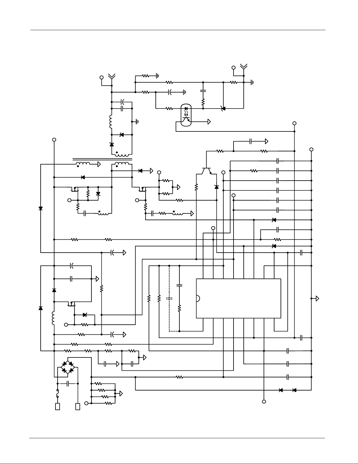
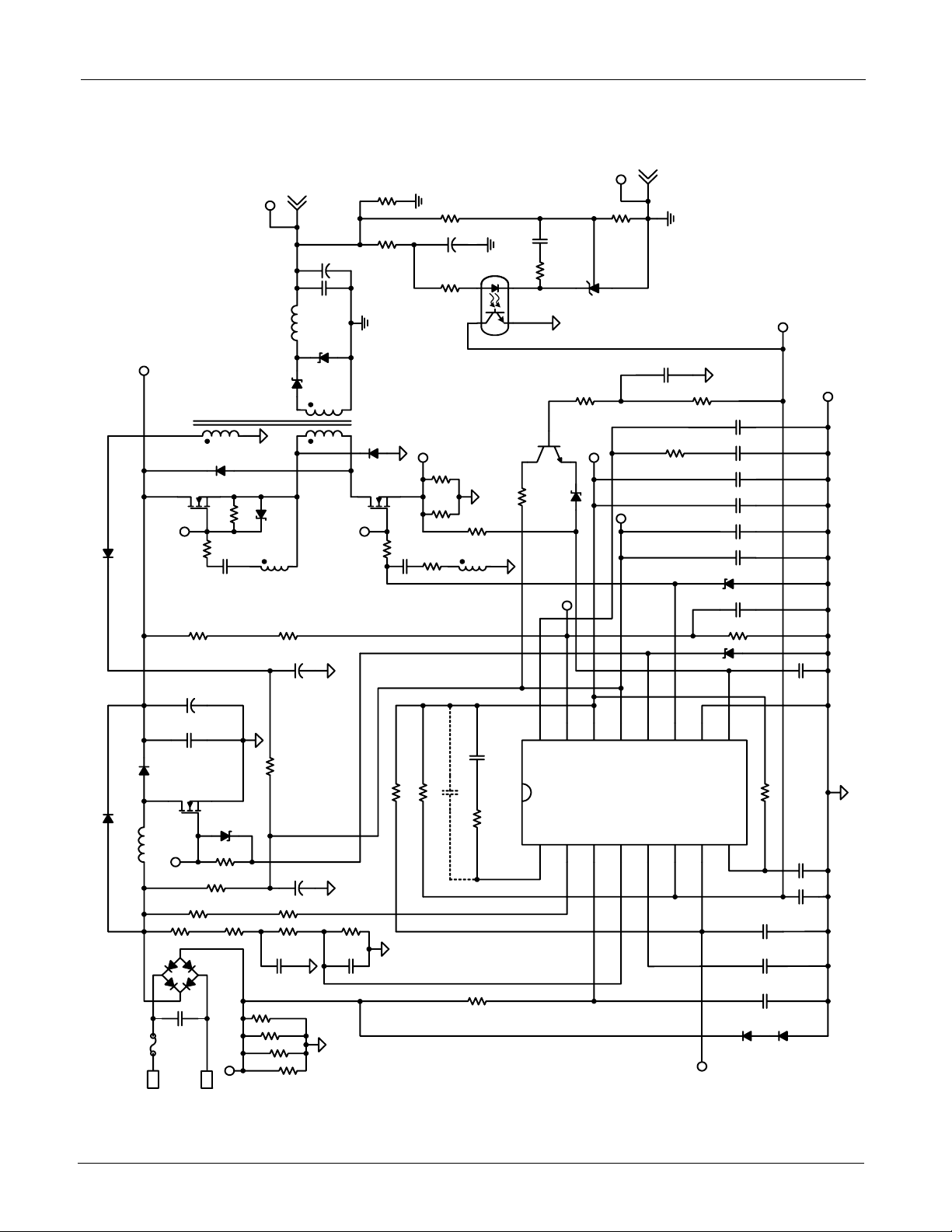
The complete power supply circuits shown in Figures 6 and
7 demonstrate the FAN4800’s ability to manage high output
power while complying with international requirements
regarding AC line quality. The PFC section provides
380V
The output of the converter delivers +12V at up to 8.4 amps.
The circuit operates from 85 to 265V
tions switching at 100kHz.
to a dual-transistor current-mode forward converter.
DC
with both power sec-
AC
D2
D1
1N5406
L1
1
2
3
4
5
6
7
8
D9
MBRS
140
R12
71.5k
IEAO
I
AC
I
SENSE
V
RMS
SS
V
DC
RAMP1
RAMP2
ISL9R460P2
FQPF9N50
NOT USED
U1
FAN4800
PFC OUT
PWM OUT
Q1
41.7k
DC I
R6
R10
6.2k
AC INPUT
85 TO 265Vac
R5A
1.2
RAMP1
R5B
1.2
D12
1N5401
D13
1N5401
I
F1
3.15A
0.68uF
SENSE
R5C
1.2
BR1
4A, 600V
C26
100nF
0.1uF
KBL06
R2A
453k
R2B
453k
C3
R3
110k
C2
0.47uF
R4
15.4k
C19
C18
1uF
470pF
C1
R5D
1.2
R31
100
R1B
500k
R1A
500k
10nF
C11
R27
75k
C30
330uF
25V
R21
Q1G
22
10nF
R28
240
C7
C6
1.5nF
VEAO
V
V
GND
LIMIT
C4
16
15
V
FB
14
REF
13
CC
12
11
10
9
The PFC Stage
Powering the FAN4800
The FAN4800 is initialized once C12 is charged to 13V
through R
age on C
well-regulated 13V for the FAN4800 from its secondary
winding. T
N
SEC
bypassing with low-ESR ceramic or film capacitors on V
and V
is achieved when D
peak AC line voltage before the boost switch Q
on. This ensures the boost inductor current is zero before
100uF
450V
C5
C12
10uF
35V
C17
220pF
D8
MBRS
140
R7A
178k
R7B
178k
and R28. PFC switching action boosts the volt-
27
to 380V via L1’s inductance. T2 then supplies a
5
’s primary-to-secondary turns ratio (N
2
) is 18.8:1. For proper circuit operation, high-frequency
is provided. Orderly PFC operation upon start-up
REF
R8
2.37k
V
FB
MBRS
C31
1nF
quick charges the boost capacitor to the
2
D3
RGF1J
Q2G
R30
4.7k
D7
MMBZ5245B
Q3G
R19
220
MMBZ5245B
V
CC
C16
1uF
R20A
2.2
0.1uF
FQPF
6N50
FQPF6N50
R9
1.1k
D4
C13
Q2
RGF1J
Q3
R20B
2.2
R11
845k
C14
1uF
D5
T2
D6
RGF1J
RAMP2 / DC I
Q4
MMBT3904
V
REF
10nF
C8
68nF
R17
33
C25
0.1uF
T1B
R14
33
C20
1uF
R15
3
T1A
D10
140
C15
10nF
VDC / +380V
LIMIT
R13
10k
C10
15uF
R16
10k
C9
PRI GND
1
V
DC
/
PRI
CC
is turned
Figure 1. The PFC Stage
© 2006 Fairchild Semiconductor Corporation www.fairchildsemi.com
FAN4800 Rev. 1.0.2 • 12/07/06
Page 2

AN6032 APPLICATION NOTE
(
(
)
(
)3(
)
(
)
η
(
)6(
(
)
(
)
(
(
PFC action begins. The value of the regulated voltage on C
must always be greater than the peak value of the maximum
line voltage delivered to the supply.
>
V2V
C5 in(rms_max)
>×
V 1.414 265
()()
C5
>
V 375V use 380V
C5
1
Because the FAN4800 uses transconductance amplifiers, the
loop compensation networks are returned to ground (see the
FAN4800 datasheet for the error amplifier characteristics/
advantages). This eliminates the interaction of the resistive
divider network with the loop compensation capacitors, permitting a wide choice of divider values chosen to minimize
amplifier offset voltages due to input bias currents. For reliable operation, R
and R7B must have a voltage rating of at
7A
least 400 volts.
Calculate the divider ratio (R
+
RRV
7A 7B C5
R2.5
8
+
R R 380
7A 7B
R2.5
8
+
RR
7A 7B
R
8
7A+R7B
)/R8 by:
=−
1
=−
=
1
151
2
Selecting the Power Components
The FAN4800 PFC section operates with continuous inductor current to minimize peak current and to maximize available power. The boost inductor value found by setting ΔI, the
peak-to-peak value of high-frequency current, is typically
10% to 20% of the peak value of the maximum line current.
2P
in(max)
I
in( peak _ max)
P
in(max)
where I
in(peak_max)
at low line, V
age, P
O(max)
ciency. Value I
is a peak value of input current occurred
in(rms_min)
is the maximum output power, and η is effi-
in(peak_max)
the specified percentage rate. I
mum current.
Δ
IdII
II
L(max) in( peak _ max)
Duty cycle D and switching frequency f
selection.
=
V
in( rms _ min)
P
O(max)
=
η
is RMS value of minimum line volt-
defines value of ΔI, where dI is
is the inductor maxi-
L(max)
=×
in( peak _ max)
Δ
=+
I
2
influence inductor
S
4
5
5
−
V2V
Oin(rms_min)
=
)
The boost diode D
D
=
L
1
=
=
=
3.128mH use 3.0mH
V
O
×
D2V
in( rms _ min)
×
fI
Δ
S
−⋅⋅
V2V V
()
O in( rms _min) in( rms _ min)
⋅⋅⋅
VfdIP
OS O(max)
−⋅⋅⋅
380 1.414 85 85 0.95
()()
{}
380 1 10 0.15 100
()
and switch Q1 are chosen with a reverse
1
5
⋅× ⋅ ⋅
()
()()
2
2
()( )
voltage rating of 500V to safely withstand the 380V boost
potential. The maximum Q
Equation 8 and the maximum Q
RMS current is obtained by
1
peak current is calculated
1
by Equation 9.
42V
=−
I2I
Q1rms in( rms _max)
2P 4 2V
O(max) in( rms _ min)
=−
ηπ
V23V
in( rms _ min) O
1.414 100 4 1.414 85
()()
=−
1.06 A
II
2.025 A
0.95 85 2 3 3.1416 380
()()
=
=+
Q1peak in( peak_ max)
2P
O(max)
=
V
η
in( rms
1.414 100
()()
=+
0.95 85
()()
=
1
23V
1
⋅⋅⋅
⋅⋅⋅
I
Δ
2
V2V 2V
()
+
_min) O S 1
⋅
⋅
in( rms _ min)
π
O
()()
1
()()
−⋅
Oin(rms_min)in(rms_min)
⋅⋅
VfL
−⋅⋅⋅
380 1.414 85 1.414 85
()()
{}
⋅× ⋅×
380 1 10 3 10
()
()( )
()()
53
The boost diode average current can be calculated by:
=
II
D1avg O(max)
P
O(max)
=
V
O
100
==
0.26 A
380
The boost capacitor value is chosen to permit a given output
voltage hold-up time in the event the line voltage is suddenly
removed.
2P t
≥
C
5
O(max) HLD
22
VV
C5(NOM ) C5(MIN )
−
where:
t
= hold-up time (sec)
HLD
V
= minimum voltage on C5 at which the PWM stage
C5(min)
can still deliver full output power
7
)
8
9
−
10
)
11
)
© 2006 Fairchild Semiconductor Corporation www.fairchildsemi.com
FAN4800 Rev. 1.0.2 • 12/07/06 2
Page 3

AN6032 APPLICATION NOTE
p
(
)12(
(
)
(
)
(
)
(
(
(
)
(
)
A key advantage of using leading/trailing-edge modulation
is that a large portion of the inductor current is "dumped"
directly into the load (PWM stage transformer) and not the
boost capacitor. This relaxes the ESR requirement of the
boost capacitor. For reference, Equation 12 should be used as
a starting point when choosing C
’s maximum ripple current
5
rating (at 120Hz).
I
O( C5 )
=
I
C5_rms
I2I
()
eak C5 _ rms
2
=⋅
12a
3. Select the value of (R
)
multiplier output current without saturating the output.
The maximum output current of the multiplier is
k
M
=
k
2
V
rms
=
kkV
Min(rms_min)
=⋅
0.35 85
()()
=≈
2528.75 2529
1A+R1B
2
2
) that permits the greatest
16
16a
228.57μA.
Selecting the Power Setting Components
The maximum average power delivered by the PFC stage is
set using the following procedure:
1. Find the resistive divider ratio that results in the voltage
at the V
pin being equal to 1.14V at the lowest line
RMS
k 2V V 0.625
+≥
RR
()
1A 1B
+≥
RR
()
1A 1B
+≥
R R 989.38k use 1M
()
1A 1B
in( rms _ min) EAO(max)
0.35 1.414 85 6 0.625
()( )()( )
()
228.57 10
⋅⋅−
228.57 10
ΩΩ
−
−
6
×
−
6
×
17
voltage. The voltage at this pin must be well filtered, yet
able to respond well to transient line voltage changes.
π
R1.14
4
=
R
22V
TOT
⋅
in( rms _ min)
13
The resistor and capacitor values in the typical example
were found empirically to offer the lowest ripple voltage
and still respond well to line voltage changes. Should a
ratio be required that is greatly different from that found
4. Select the value of the current sense resistor to complete
the calculations for the power setting components.
⋅−⋅
R k V 0.625
MULO M EAO( max)
R||R||R||R
5A 5B 5C 5D
R||R||R||R
5A 5B 5C 5D
R || R || R || R 0.452 use 0.3
5A 5B 5C 5D
≤
3.5 10 2529 6 0.625 0.95
()
≤
≤
(
PRR
O(max) 1A 1B
3
×⋅ − ⋅
ΩΩ
+
()
()( )()
100 1 10
()
()
×
η
18
6
in Equation 13, adjust the filter capacitor values according to Equations 14 and 15.
C
=
3
2f R R R R
⋅+⋅+
π
()()
12A2B 34
⎛⎞
1
+
⎜⎟
⎜⎟
RR RR
()()
2A 2B 3 4
⎝⎠
C
=
2
R
TOT
RR
⋅
4TOT
+⋅+
2f R
⋅
π
24
14
15
where:
R
= multiplier output termination resistance (3.5kΩ).
MULO
Voltage Loop Compensation
Maximum transient response of the PFC section, without
instability, is obtained when the open-loop crossover frequency is one-half the line frequency. For this application,
where:
f
= 15Hz, f2 = 23Hz
1
R
= R2A + R2B + R3 + R
TOT
4
the compensation components (pole/zero pair) are chosen so
that the closed loop response decreases at 20dB/decade,
crossing unity gain at 30Hz, then immediately decreasing at
40dB/decade. The error amplifier pole is placed at 30Hz and
an effective zero at one-tenth this frequency, or 3Hz. Find
2. Find the constant of proportionality kM of the multiplier
gain k in Equation 16a. To obtain "brownout" action
the crossover frequency (G
reference, Equation 20 finds the power stage pole and Equation 21 finds the power stage DC gain.
= 1) of the power stage. For
PS
below the lowest input voltage, the maximum gain of the
multiplier must be used when finding k
gain (0.35) occurs when the V
RMS
. The maximum
M
input of the multiplier
is 1.14V. Equation 16 is the general expression for the
multiplier gain versus the line voltage.
)
)
)
© 2006 Fairchild Semiconductor Corporation www.fairchildsemi.com
FAN4800 Rev. 1.0.2 • 12/07/06 3
Page 4
AN6032 APPLICATION NOTE
(
(
(
(
(
)
(
)
(
(
⋅
(
(
V
BOOST
R7
FB
G
RDIV
=
15
2.5V
16
VEAO
R11R8
C8
C9
=× −
6.613 10 43.59dB
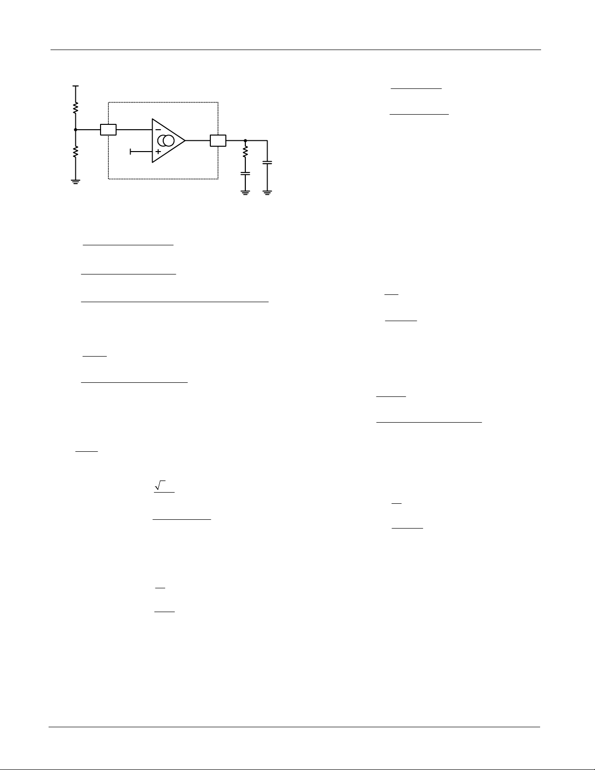
The amount of error amplifier gain required to bring the
open-loop gain to unity at 30Hz is the negative of the sum of
R
=
8
++
RRR
7A 7B 8
2.37
++
178 178 2.37
3
−
23
()
the power stage, plus divider stage gain (attenuation):
f
C
82.02Hz
f
P
2.20Hz
where:
=
R
L
Figure 2. Voltage Amp Compensation
P
=
π
2 V V 0.625 C
=
πη
2 V V 0.625 C
=
2 3.1416 0.95 380 6 0.625 100 10
()( )( )( )( )
in(max)
()
OEAO(max) 5
O EAO(max ) 5
−
P
O(max)
()
−
100
⋅⋅⋅⋅−⋅×
()
=
1
=
π
RC
L5
=
3.1416 1444 100 10
()()
1
6
⋅⋅×
()
−
=
2
V
O
P
O(max)
2f
C
=
G
PS( DC )
52.72 34.44dB
f
P
⋅
1.414 82.02
()()
=
2.20
=
()
=− +
GG G
EA PS( 30 Hz ) RDIV
=− + −
8.736 43.59
()
=
34.854dB 55.29V / V
The value of R
19
6
−
20
error amplifier, can be determined by:
)
)
Calculate C
, which sets the high-frequency gain of the
11
G
EA
R
=
11
g
M
55.29
=
70 10
×
789.8k use 845kΩ
=
; which, together with R11, sets the zero fre-
8
()
()
6
−
Ω
24
25
)
)
quency at 3Hz.
1
=
C
8
2Rf
π
11 Z
=
2 3.1416 845 10 3
()( )
62.8nF use 68nF
=
1
⋅×⋅
()
3
()
26
)
Since the pole frequency is ten times the zero frequency, the
21
pole capacitor C
)
is one-tenth the value of C8.
9
C
8
=
C
9
10
9
−
×
68 10
=
10
=
6.8nF use 10nF
27
)
The gain of the power stage at 30Hz is calculated by:
Current Loop Compensation
f
G
PS( 30 Hz )
2.734 8.736dB
=
=
=
C
30
82.02
30
()
The power stage gain is attenuated by the resistive divider
(R
7A+R7B
© 2006 Fairchild Semiconductor Corporation www.fairchildsemi.com
FAN4800 Rev. 1.0.2 • 12/07/06 4
)/R8 according to Equation 23:
22
)
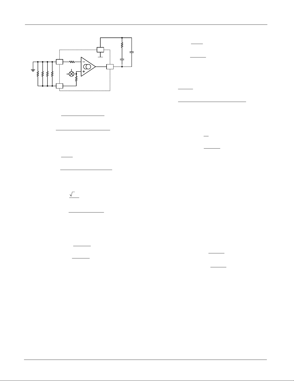
The current loop is compensated like the voltage loop,
except the choice of the open-loop crossover frequency. To
prevent interaction with the voltage loop, the current loop
bandwidth should be greater than ten times the voltage loop
crossover frequency, but no more than one sixth the switching frequency, or 16.7kHz. The power stage crossover frequency is calculated by Equation 28, the pole frequency by
Equation 29, and the power stage DC gain by Equation 30.
Page 5
AN6032 APPLICATION NOTE
(
)28(
)
(
(
)
(
)
Ω
(
(
)
(
)
(
G
EA
=
V
REF
R5AR5BR5CR
I
SENSE
GND
5D
3.5k
10
VEAO
I
AC
3.5k
3
Figure 3. Current Amp Compensation
R ||R ||R ||R V
()
5A 5B 5C 5D O
=
f
C
=
2 3.1416 3 10 2.75
()( )
=
2.2kHz
f
=
P
=
2.20Hz same as (20)
=
π
2LV
1 RAMP
−
(P P)
0.3 380
()( )
⋅⋅×⋅
−
3
()
1
RC
π
L5
1
3.1416 1444 100 10
()()
⋅⋅×
()
14
V
REF
R12
C6
1
IEAO
()
−
6
C7
29
R
12
g
M(CE)
7.58
=
×
85 10
=
89.2k use 71.5k
Calculate the value of C
1
=
C
6
π
2Rf
12 Z
=
1.33nF use 1.5nF
The pole capacitor C
⋅⋅×⋅×
2 3.1416 71.5 10 1.67 10
()( )
=
is one-tenth the value of C6.
7
C
150 pF
The PWM Stage
6
−
Ω
to form the zero at 1.67kHz.
6
1
()()
C
=
7
10
1.5 10
=
33
6
9
−
×
10
=
33
34
35
)
Soft-Starting the PWM Stage
2f
G
PS( DC )
1414 63
C
=
f
P
1.414 2.20 10
⋅×
()
=
=
()
2.20
.0dB
()
30
3
Find the gain of the power stage at 16.7kHz.
f
G
PS( 16.7 kHz )
1.32 10 17.60dB
C
=
16.7 10
2.20 10
=
16.7 10
=× −
3
×
3
×
3
×
1
−
()
31
The current loop contains no attenuating resistors, so find the
error amplifier gain with:
=− −
GG
(
EA PS (16.7 kHz )
=− −
17.60
()
=
17.60dB 7.58V / V
()
32
Determine the value of the current error amplifier setting
resistor R
12
.
The FAN4800 features a dedicated soft-start pin for control-
)
ling the rate of rise of the output voltage and preventing
overshoot during power on. The controller does not initiate
soft-start action until the PFC voltage reaches its nominal
value, thereby preventing stalling of the output voltage due
to excessive PFC currents. PWM action is terminated in the
event the FAN4800 loses power or if the PFC boost voltage
falls below 228V
. The soft-start capacitor value (C19) for
DC
50ms of delay is found by Equation 36.
)
⎛⎞
=⋅
Ct
()
19 SS
=⋅
0.05
=
1 F
⎜⎟
⎝⎠
()
μ
−
6
×
20 10
0.95
−
×
20 10
0.95
6
⎛⎞
⎜⎟
⎝⎠
Setting the Oscillator Frequency
There is one version of the FAN4800. The FAN4800IN is
where the PFC and PWM run at the same frequency.
FAN4800IN
In general, it is best to choose a small-valued capacitor C
to maximize the oscillator duty cycle (minimize the C18 discharge time). Too small a value capacitor can increase the
oscillator’s sensitivity to phase modulation caused by stray
field voltage induction into this node. For the practical
36
)
18
© 2006 Fairchild Semiconductor Corporation www.fairchildsemi.com
FAN4800 Rev. 1.0.2 • 12/07/06 5
Page 6
AN6032 APPLICATION NOTE
(
(
(
)
D3
RGF1J
Q2G
R30
4.7k
D7
MMBZ5245B
Q3G
R19
220
MMBZ5245B
V
CC
C16
1uF
R20A
2.2
R9
1.1k
D4
C13
0.1uF
Q2
FQPF
6N50
Q3
FQPF6N50
R20B
R11
845k
C14
1uF
D5
RGF1J
D6
RGF1J
RAMP2 / DC I
2.2
MMBT3904
V
REF
C8
68nF
T2
Q4
10nF
C5
100uF
450V
R6
41.7k
R10
6.2k
C7
NOT USED
U1
FAN4800
PFC OUT
PWM OUT
DC I
C6
1.5nF
VEAO
V
V
GND
LIMIT
16
15
V
FB
14
REF
13
CC
12
11
10
9
R12
71.5k
1
IEAO
2
I
AC
3
I
SENSE
4
V
RMS
5
SS
6
V
DC
7
RAMP1
8
RAMP2
C18
C19
470pF
1uF
10nF
C11
C12
10uF
35V
C17
220pF
MBRS
140
R7A
178k
R7B
178k
D8
R8
2.37k
R17
33
C25
0.1uF
T1B
R14
33
C20
1uF
R15
3
T1A
V
FB
D10
MBRS
140
C15
C31
10nF
1nF
R13
10k
R16
10k
C9
D11A
MBR2545CT
D11B
MBR2545CT
LIMIT
PRI GND
VDC / +380V
C10
15uF
L2
MOC8112
TL431A
V
12V
12V,
2.26k
100W
R18
220
R22
8.66k
R25
12V RET
12V
RETURN
C24
1uF
C21
2200uF
25V
R24
1.2k
R23
C22
1.5k
4.7uF
U2
R26
C23
10k
100nF
U3
DC
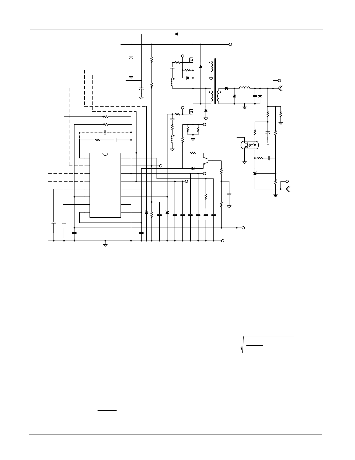
Figure 4. The PWM Stage
example, a 470pF capacitor is chosen for C18. Equation 37 is
accurate with values of R
R
≅
6
≅
0.51 1 10 470 10
()
41.7k
≅
greater than 10k.
6
1
0.51 f C
⋅
SW 18
1
512
⋅× ⋅ ×
()( )
−
Ω
37
Current Limit
The PWM power stage operates in current mode using R
and R
to generate the voltage ramp for duty cycle control.
20B
The FAN4800 limits the maximum primary current via an
internal 1V comparator; which, when exceeded, terminates
the drive to the external power MOSFETs. Maximum primary current is:
1
PRI ( MAX )
=
R||R
20 A 20B
2.2 2.2
=
2.2 2.2
=
+
×
I
0.91 Amps
20A
38
Voltage Mode (Feedforward)
Should voltage mode control be used, it is necessary to know
C
’s peak voltage to choose the correct ramp generating
)
)
5
components. Equation 39 finds the worst-case peak-to-peak
ripple voltage across C
. To find the peak voltage, divide the
5
ripple voltage by two and add it to the regulated boost voltage. Remember that since the FAN4800 employs leading/
trailing modulation, the actual peak-to-peak ripple voltage is
generally much less than the calculated value.
VI ESRC
=+
R( C5 ) OUT( C5 ) 5
⎛⎞
⎜⎟
4fC
⎝⎠
2
1
π
L5
()
where:
f
= line frequency.
L
Solve Equation 40 for the ramp resistor value. The ramp
capacitor value should be in the range of 470pF ~ 10nF.
Choose a resistor with an adequate voltage rating to withstand the boost voltage.
2
39
© 2006 Fairchild Semiconductor Corporation www.fairchildsemi.com
FAN4800 Rev. 1.0.2 • 12/07/06 6
Page 7
AN6032 APPLICATION NOTE
(
(
)
N
(
)
P
(
)
(
)
Output Voltage Compensation
σ
R
=
RAMP
Cfln1
RAMP SW
(MAX)
⎛⎞
V
REF
−
⎜⎟
+
V0.5V
OR
⎝⎠
40
where:
σ
= maximum PWM duty cycle
(MAX)
(0.45 for the FAN4800)
V
= peak-to-peak boost capacitor ripple voltage for
R
Equation 39.
The Power Transformer Turns Ratio
The minimum output voltage at the secondary of T2 is found
in Equation 41. The secondary voltage is chosen to be 30
volts to increase the output voltage hold-up time.
V
OUT
VV
1.0
27.7Volts
=+
SEC( MIN ) F
σ
(MAX)
12
=+
0.45
=
The transformer turns ratio is derived from Equation 42:
NV
PRI O
=
NV
SEC SEC( MIN )
380
=
30
=
:N 38:3
PRI SEC
The maximum secondary current with the output shorted is
limited by Equation 43:
41
42
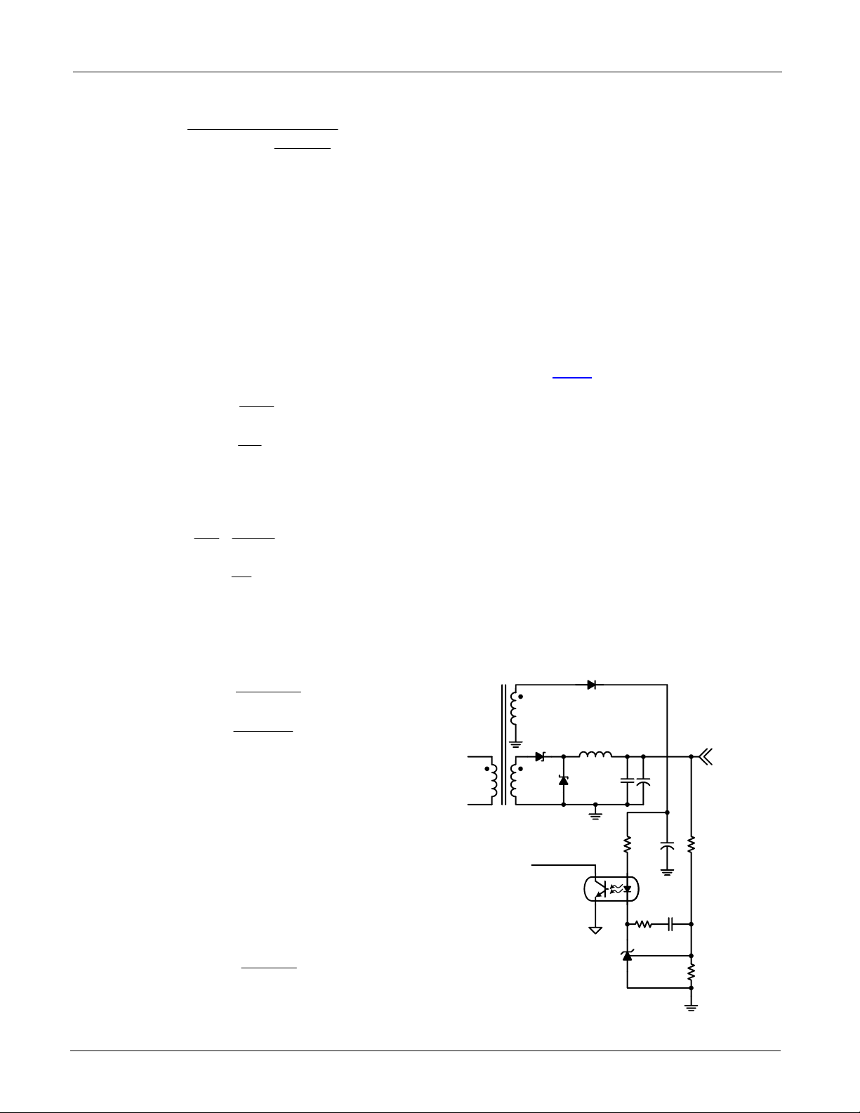
A TL431 shunt regulator U3 and opto-isolator U2 perform
output voltage setting and regulation. The opto crosses the
)
primary-to-secondary safety boundary, varying the voltage
on the V
pin to keep the output voltage constant against
DC
line and load changes. Using current-mode control simplifies
loop compensation, leaving only a single pole and zero in the
output stage. The pole is created from the output capacitor
and equivalent load resistance. The zero is formed from the
filter capacitor and its ESR. In this example, the action of the
zero occurs well after the closed-loop response has crossed
unity, so it was not compensated with a pole. The output pole
is canceled, increasing the overall bandwidth by the addition
of R
and C23, which form a zero with TL431. For more
26
information on using the TL431, including gain/phase versus
frequency characteristics, refer to the Fairchild Semiconductor datasheet for the TL431
.
3.3V Output Design Changes
The latest microprocessors and support circuitry require a
3.3V supply for proper operation. The FAN4800 is ideal for
these applications, including the energy-efficient, ecologically friendly "Green" PC. If the total output power required
varies greatly from 100 watts, it is necessary to re-select certain components, beginning with the PFC stage. T
ratio must be adjusted according to Equation 42 and another
low-current secondary winding added using the same turns
ratio as originally found for the +12 volts. This second winding is necessary to power the TL431/opto circuit because the
3.3V output is not adequate to fully bias the feedback circuitry. C
age. Figure 5 displays a 3.3V output stage capable of
supplying 16 amps.
may be increased to reduce the output ripple volt-
21
’s turn
2
IN
SEC( MAX )
=
N
SEC
⋅
0.91 38
()()
=
3
=
I
11.5 Amps
RI ( MAX ) PRI
The output inductor and rectifier are chosen with maximum
current rating larger than the maximum secondary current.
Output Filter Component Filter Selection
L2’s value is chosen to efficiently minimize output ripple
43
UF4001
V
R22
10.2k
OUTPUT
3.3V, 16A
L2
D11A
D11B
T2
C24
R23
U2
MOC8112
C21
C22
current, thereby easing the ESR requirement of the filter
capacitor. C
’s ESR value is the dominant contributor to the
21
output ripple. The maximum ESR value required is found in
Equation 44:
ESR
(C21)
VLf
≤
V
SEC ( MAX )
R2SW
σ
44
U3
TL431A
R26
C23
R25
31.6k
where:
V
= peak-to-peak output ripple voltage.
R
© 2006 Fairchild Semiconductor Corporation www.fairchildsemi.com
FAN4800 Rev. 1.0.2 • 12/07/06 7
Figure 5. 3.3V Output Stage
Page 8
AN6032 APPLICATION NOTE
12V
RETURN
12V,
100W
12V
C21
1uF
C24
L2
T2; PREMIER MAGNETICS TSO-735
NOTE : L1; PREMIER MAGNETICS TDS-1047
VDC / +380V
D3
RGF1J
T1; PREMIER MAGNETICS PMGO-03
L2; PREMIER MAGNETICS VTP-05007
MBR2545CT
MMBZ5245B
R7B
D11B
MBR2545CT
178k
35V
C12
10uF
D11A
D5
RGF1J
Q2
6N50
FQPF
R30
4.7k
D7
Q2G
33
C25
R17
0.1uF
T1B
R7A
178k
220
R18
R22
8.66k
C23
25V
R24
1.2k
2200uF
T2
D6
RGF1J
Q3
FQPF6N50
Q3G
33
R14
C22
4.7uF
R23
1.5k
U2
MOC8112
LIMIT
RAMP2 / DC I
2.2
R20B
R9
R19
T1A
1.1k
220
2.2
R20A
3
1uF
C20
R15
100nF
10k
R26
Q4
MMBT3904
D4
MMBZ5245B
FB
V
12V RET
R25
2.26k
U3
TL431A
C10
15uF
DC
V
PRI GND
10k
R11
R16
C9
10nF
C8
68nF
845k
1uF
C14
C13
0.1uF
1uF
C16
C15
10nF
140
D10
MBRS
1nF
C31
R8
2.37k
D8
140
MBRS
C17
220pF
10k
R13
REF
V
CC
V
C5
450V
100uF
C4
D1
ISL9R460P2
D2
1N5406
L1
BR1
4A, 600V
F1
3.15A
10nF
Q1
FQPF9N50
Q1G
75k
R27
R1A
500k
R2A
453k
KBL06
C1
0.68uF
AC INPUT
85 TO 265Vac
240
R28
D9
140
MBRS
22
R21
25V
C30
330uF
R1B
500k
453k
1.2
R5C
R3
110k
C2
C3
0.1uF
1.2
1.2
R5B
1.2
R5A
R2B
R5D
SENSE
I
R6
R10
41.7k
R4
15.4k
0.47uF
C6
1.5nF
C7
6.2k
NOT USED
R12
71.5k
100
R31
16
15
14
13
12
11
10
FB
V
VEAO
U1
CC
REF
V
V
PFC OUT
PWM OUT
9
LIMIT
GND
DC I
FAN4800
IEAO
I
1
2
V
I
3
4
RMS
SENSE
AC
DC
V
SS
5
6
RAMP1
7
RAMP2
8
D12
C11
10nF
C18
470pF
1uF
C19
C26
100nF
D13
1N5401
1N5401
RAMP1
Figure 6. Complete 100W Circuit (Current Mode)
© 2006 Fairchild Semiconductor Corporation www.fairchildsemi.com
FAN4800 Rev. 1.0.2 • 12/07/06 8
Page 9
AN6032 APPLICATION NOTE
12V
RETURN
12V,
100W
12V
C21
1uF
C24
L2
T2; PREMIER MAGNETICS TSO-735
NOTE : L1; PREMIER MAGNETICS TDS-1047
VDC / +380V
D3
RGF1J
T1; PREMIER MAGNETICS PMGO-03
L2; PREMIER MAGNETICS VTP-05007
MBR2545CT
MMBZ5245B
R7B
D11B
MBR2545CT
178k
35V
C12
10uF
D11A
D5
RGF1J
Q2
6N50
FQPF
R30
4.7k
D7
Q2G
33
C25
R17
0.1uF
T1B
R7A
178k
220
R18
R22
8.66k
C23
25V
R24
1.2k
2200uF
T2
D6
RGF1J
Q3
FQPF6N50
Q3G
33
R14
C22
4.7uF
R23
1.5k
U2
MOC8112
LIMIT
RAMP2 / DC I
2.2
R20B
R9
R19
T1A
1.1k
220
2.2
R20A
3
1uF
C20
R15
100nF
10k
R26
Q4
MMBT3904
D4
MMBZ5245B
FB
V
12V RET
R25
2.26k
U3
TL431A
C10
15uF
DC
V
PRI GND
10k
R11
R16
C9
10nF
C8
68nF
845k
1uF
C14
C13
0.1uF
1uF
C16
C15
10nF
140
D10
MBRS
1nF
C31
R8
2.37k
D8
140
MBRS
C17
220pF
10k
R13
REF
V
CC
V
C5
450V
100uF
C4
D1
ISL9R460P2
D2
1N5406
L1
BR1
4A, 600V
F1
3.15A
10nF
Q1
FQPF9N50
Q1G
75k
R27
R1A
500k
R2A
453k
KBL06
C1
0.68uF
AC INPUT
85 TO 265Vac
240
R28
D9
140
MBRS
22
R21
25V
C30
330uF
R1B
500k
453k
1.2
R5C
R3
110k
C2
C3
0.1uF
1.2
1.2
R5B
1.2
R5A
R2B
R5D
SENSE
I
R6
R10
41.7k
R4
15.4k
0.47uF
C6
1.5nF
C7
6.2k
NOT USED
R12
71.5k
100
R31
16
15
14
13
12
11
10
FB
V
VEAO
U1
CC
REF
V
V
PFC OUT
PWM OUT
9
LIMIT
GND
DC I
R29
61.9k
FAN4800
IEAO
I
1
2
V
I
3
4
RMS
SENSE
AC
DC
V
SS
5
6
RAMP1
7
RAMP2
8
D12
C27
470pF
C11
10nF
C18
470pF
1uF
C19
C26
100nF
D13
1N5401
1N5401
RAMP1
Figure 7. Complete 100W Circuit (Voltage Mode)
© 2006 Fairchild Semiconductor Corporation www.fairchildsemi.com
FAN4800 Rev. 1.0.2 • 12/07/06 9
Page 10

AN6032 APPLICATION NOTE
DISCLAIMER
FAIRCHILD SEMICONDUCTOR RESERVES THE RIGHT TO MAKE CHANGES WITHOUT FURTHER NOTICE TO ANY PRODUCTS
HEREIN TO IMPROVE RELIABILITY, FUNCTION, OR DESIGN. FAIRCHILD DOES NOT ASSUME ANY LIABILITY ARISING OUT OF THE
APPLICATION OR USE OF ANY PRODUCT OR CIRCUIT DESCRIBED HEREIN; NEITHER DOES IT CONVEY ANY LICENSE UNDER ITS
PATENT RIGHTS, NOR THE RIGHTS OF OTHERS.
LIFE SUPPORT POLICY
FAIRCHILD’S PRODUCTS ARE NOT AUTHORIZED FOR USE AS CRITICAL COMPONENTS IN LIFE SUPPORT DEVICES OR SYSTEMS
WITHOUT THE EXPRESS WRITTEN APPROVAL OF THE PRESIDENT OF FAIRCHILD SEMICONDUCTOR CORPORATION.
As used herein:
1.Life support devices or systems are devices or systems which,
(a) are intended for surgical implant into the body, or
(b) support or sustain life, or
(c) whose failure to perform when properly used in accordance with
2.A critical component is any component of a life support device or
system whose failure to perform can be reasonably expected to
cause the failure of the life support device or system, or to affect its
safety or effectiveness.
instructions for use provided in the labeling, can be reasonably
expected to result in significant injury to the user.
© 2006 Fairchild Semiconductor Corporation www.fairchildsemi.com
FAN4800 Rev. 1.0.2 • 12/07/06 10
 Loading...