

Page 1
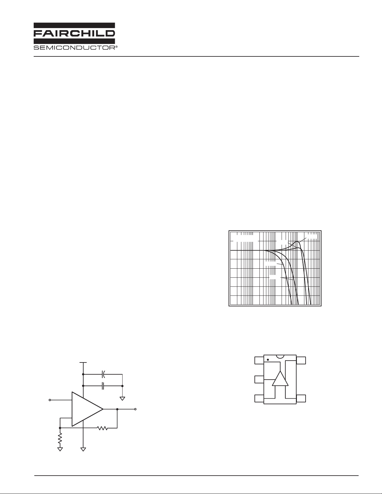
Features at +1.2V
• 640µA supply current per amplifier
• 36MHz gain bandwidth product
• Output voltage range: 0.06V to 1.10V
• Input voltage range: -0.4V to +0.2V
• 8V/µs slew rate
• 12nV/√Hz input voltage noise
• Package option (SC70-5)
• Fully specified at +1.2V, +2.7V, and +5V supplies
Applications
• Cellular phones
• Personal data assistants
• A/D buffer
• DSP interface
• Smart card readers
• Portable test instruments
• Single cell NiCd/Ni MH powered systems
• Keyless entry
• Infrared receivers for remote controls
• Telephone systems
• Audio applications
Description
The FAN4113 is a low cost, voltage feedback amplifier that
consumes only 640µA of supply current. The FAN4113 is
designed to operate from +1.2V to 5.5V (±2.75V) supplies.
The common mode voltage range extends below the negative
rail and the output provides rail-to-rail performance.
The FAN4113 is designed on a complementary bipolar
process and provides 36MHz of bandwidth and 8V/µs of slew
rate at a low supply voltage of 1.2V. The combination of low
power, rail-to-rail performance, low voltage operation, and
tiny package options make the FAN4113 well suited for use
in personal electronics equipment such as cellular handsets,
pagers, PDAs, and other battery powered applications.
FAN4113
1.2V, 36MHz, Low Power Rail-to-Rail Amplifier
www.fairchildsemi.com
REV. 1 October 2001
Typical Application
Pin Assignments
-
+
1
2
3
Out
-V
s
+In
+V
s
-In
5
4
Non-Inverting Freq. Response, Vs = 1.2V
Vo = 50mV
pp
G = 1
G = 10
G = 5
G = 2
+V
s
6.8µF
+
+
FAN4113
-
0.01µF
R
f
+In
R
g
Normalized Magnitude (1dB/div)
0.01
0.1
1
Frequency (MHz)
10 100
Out
Page 2
Absolute Maximum Ratings
Parameter Min. Max. Unit
Supply Voltages 0+6V
Maximum Junction Temperature – +175 °C
Storage Temperature Range -65 +150 °C
Lead Temperature, 10 seconds – +260 °C
Operating Temperature Range, recommended -40 +85 °C
Input Voltage Range -
Vs-0.5 +Vs+0.5
V
θjafor 5 load SC70 331.4°C/W
Electrical Specifications
(Tc= 25°C, Vs= +1.2V, G = 2, RL= 5kΩ to Vs/2, Rf= 5kΩ, V
o (DC)
= Vcc/2; unless otherwise noted)
Parameter Conditions Min. Typ. Max. Unit
AC Performance
-3dB Bandwidth
1
G = +2, Vo= 50mV
pp
20 MHz
Full Power Bandwidth G = +2, Vo= 500mV
pp
9 MHz
Gain Bandwidth Product 36 MHz
Rise and Fall Time 200mV
pp
25 ns
Overshoot 200mV
pp
6 %
Slew Rate 500mV
pp
8 V/µs
2nd Harmonic Distortion 0.5Vpp, 500kHz 75 dBc
3rd Harmonic Distortion 0.5Vpp, 500kHz 84 dBc
THD 0.5Vpp, 500kHz 0.018 %
Input Voltage Noise >100kHz 12 nV/√Hz
DC Performance
Input Offset Voltage 0.5 mV
Average Drift 2 µV/°C
Input Bias Current 400 nA
Average Drift 2 nA/°C
Input Offset Current 30 nA
Power Supply Rejection Ratio DC 80 dB
Open Loop Gain 65 dB
Supply Current 640 µA
Input Characteristics
Input Resistance 25 MΩ
Input Capacitance 1.8 pF
Input Common Mode Voltage Range -0.4 to 0.2 V
Common Mode Rejection Ratio 72 dB
Output Characteristics
Output Voltage Swing RL= 5kΩ to Vs/2 0.05 to 1.11 V
RL= 1kΩ to Vs/2 0.07 to 1.03 V
Output Current ±1.2 mA
Short Circuit Output Current ±1.8 mA
Power Supply Operating Range 1.2 1.2 5.5 V
Min/max ratings are based on product characterization and simulation. Individual parameters are tested as noted. Outgoing quality levels are
determined from tested parameters.
Notes:
1. For G = +1, Rf= 0.
DATA SHEET FAN4113
2 REV. 1 October 2001
Page 3
Electrical Specifications
(Tc= 25°C, Vs= +2.7V, G = 2, RL= 5kΩ to Vs/2, Rf= 5kΩ, V
o (DC)
= Vcc/2; unless otherwise noted)
Parameter Conditions Min. Typ. Max. Unit
AC Performance
-3dB Bandwidth
1
G = +1, Vo= 50mV
pp
42 MHz
G = +2, Vo= 50mV
pp
20 MHz
Full Power Bandwidth G = +2, Vo= 500mV
pp
9 MHz
Gain Bandwidth Product 35 MHz
Rise and Fall Time 200mV
pp
25 ns
Settling Time to 1% 1V
pp
200 ns
Overshoot 200mV
pp
4 %
Slew Rate 1V
pp
8 V/µs
2nd Harmonic Distortion 0.5Vpp, 500kHz 75 dBc
3rd Harmonic Distortion 0.5Vpp, 500kHz 84 dBc
THD 0.5Vpp, 500kHz 0.018 %
Input Voltage Noise >100kHz 12 nV/√Hz
DC Performance
Input Offset Voltage
2
-2.5 0.5 +2.5 mV
Average Drift 2 µV/°C
Input Bias Current
2
400 800 nA
Average Drift 2 nA/°C
Input Offset Current 30 nA
Power Supply Rejection Ratio
2
DC 66 80 dB
Open Loop Gain 70 dB
Supply Current
2
750 900 µA
Input Characteristics
Input Resistance 25 MΩ
Input Capacitance 1.4 pF
Input Common Mode Voltage Range -0.4 to 1.7 V
Common Mode Rejection Ratio
2
66 75 dB
Output Characteristics
Output Voltage Swing RL= 5kΩ to Vs/2
2
0.085 to 2.55 0.04 to 2.64 V
RL= 1kΩ to Vs/2 0.07 to 2.56 V
Output Current ±9 mA
Short Circuit Output Current ±11 mA
Power Supply Operating Range 1.2 2.7 5.5 V
Min/max ratings are based on product characterization and simulation. Individual parameters are tested as noted. Outgoing quality levels are
determined from tested parameters.
Notes:
1. For G = +1, Rf= 0.
2. 100% tested at +25°C.
FAN4113 DATA SHEET
REV. 1 October 2001 3
Page 4
Electrical Specifications
(Tc= 25°C, Vs= +5V, G = 2, RL= 5kΩ to Vs/2, Rf= 5kΩ, V
o (DC)
= Vcc/2; unless otherwise noted)
Parameter Conditions Min. Typ. Max. Unit
AC Performance
-3dB Bandwidth
1
G = +1, Vo= 50mV
pp
36 MHz
G = +2, Vo= 50mV
pp
20 MHz
Full Power Bandwidth G = +2, Vo= 500mV
pp
9 MHz
Gain Bandwidth Product 31 MHz
Rise and Fall Time 200mV
pp
25 ns
Settling Time to 1% 2V
pp
250 ns
Overshoot 200mV
pp
2 %
Slew Rate 2V
pp
8 V/µs
2nd Harmonic Distortion 0.5Vpp, 500kHz 75 dBc
3rd Harmonic Distortion 0.5Vpp, 500kHz 84 dBc
THD 0.5Vpp, 500kHz 0.018 %
Input Voltage Noise >100kHz 12 nV/√Hz
DC Performance
Input Offset Voltage 0.5 mV
Average Drift 2 µV/°C
Input Bias Current 400 nA
Average Drift 2 nA/°C
Input Offset Current 30 nA
Power Supply Rejection Ratio DC 80 dB
Open Loop Gain 70 dB
Supply Current 750 µA
Input Characteristics
Input Resistance 25 MΩ
Input Capacitance 1.25 pF
Input Common Mode Voltage Range -0.4 to 4.0 V
Common Mode Rejection Ratio 76 dB
Output Characteristics
Output Voltage Swing RL= 5kΩ to Vs/2 0.03 to 4.92 V
RL= 1kΩ to Vs/2 0.07 to 4.79 V
Output Current ±9 mA
Short Circuit Output Current ±13 mA
Power Supply Operating Range 1.2 5 5.5 V
Min/max ratings are based on product characterization and simulation. Individual parameters are tested as noted. Outgoing quality levels are
determined from tested parameters.
Notes:
1. For G = +1, Rf= 0.
DATA SHEET FAN4113
4 REV. 1 October 2001
Page 5
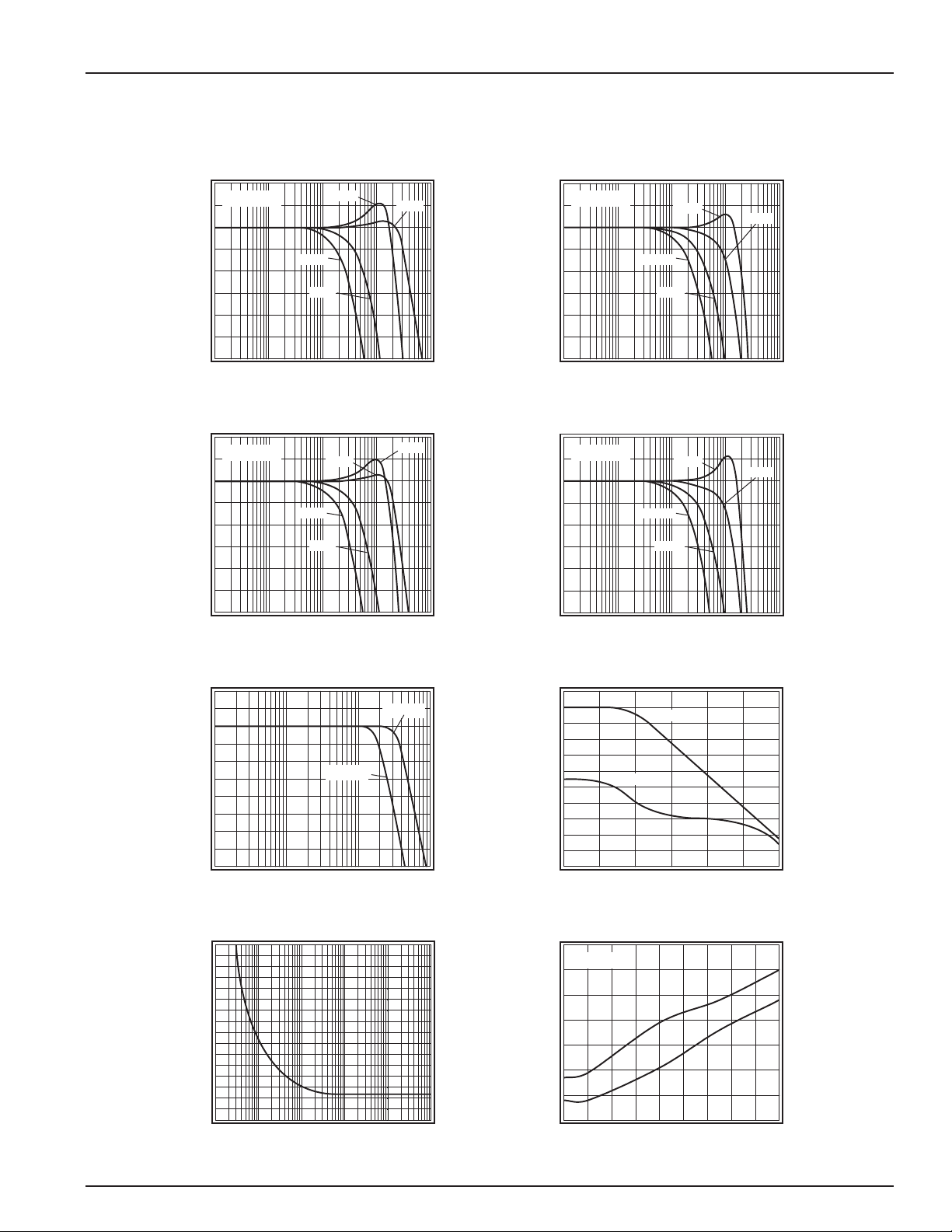
Typical Operating Characteristics
(Tc= 25°C, Vs= +2.7V, G = 2, RL= 5kΩ to Vs/2, Rf= 5kΩ, V
o (DC)
= Vcc/2; unless otherwise noted)
FAN4113 DATA SHEET
REV. 1 October 2001 5
Non-Inverting Frequency Response
G = 10
G = 5
G = 2
G = 1
Vo = 50mV
pp
Normalized Magnitude (1dB/div)
0.01
0.1
1
10 100
Frequency (MHz)
Non-Inverting Freq. Response, Vs = 1.2V
Vo = 50mV
pp
G = 1
G = 10
G = 5
G = 2
Normalized Magnitude (1dB/div)
0.01
0.1
1
10 100
Frequency (MHz)
Inverting Frequency Response
Vo = 50mV
pp
G = -1
G = -10
G = -5
Normalized Magnitude (1dB/div)
0.01
0.1
1
10 100
Frequency (MHz)
Inverting Freq. Response, Vs = 1.2V
Vo = 50mV
pp
G = -1
G = -10
G = -5
Normalized Magnitude (1dB/div)
0.01
0.1
1
10 100
Frequency (MHz)
G = -2
G = -2
Large Signal Frequency Response
Vo = 2V
Magnitude (1dB/div)
0.01
0.1
Frequency (MHz)
Input Voltage Noise
80
70
60
50
40
30
20
Voltage Noise (nV/√Hz)
10
0
0.001
0.01
0.1 10.0001
Frequency (MHz)
Open Loop Gain & Phase vs. Frequency
80
Vo = 1V
pp
pp
1
10
70
60
50
40
30
20
10
0
Open Loop Gain (dB)
-10
-20
-30
100
Phase
1k 10k 100k 1M 10M 100M
|Gain|
Phase (degrees)
-10
-48
-86
-124
-162
-200
Frequency (Hz)
Harmonic Distortion vs. Frequency
-60
Vo = 500mV
-65
-70
-75
-80
-85
Distortion (dBc)
-90
10
-95
100 200 300 400 500 600 700 800 900
pp
2nd
3rd
1000
Frequency (KHz)
Page 6
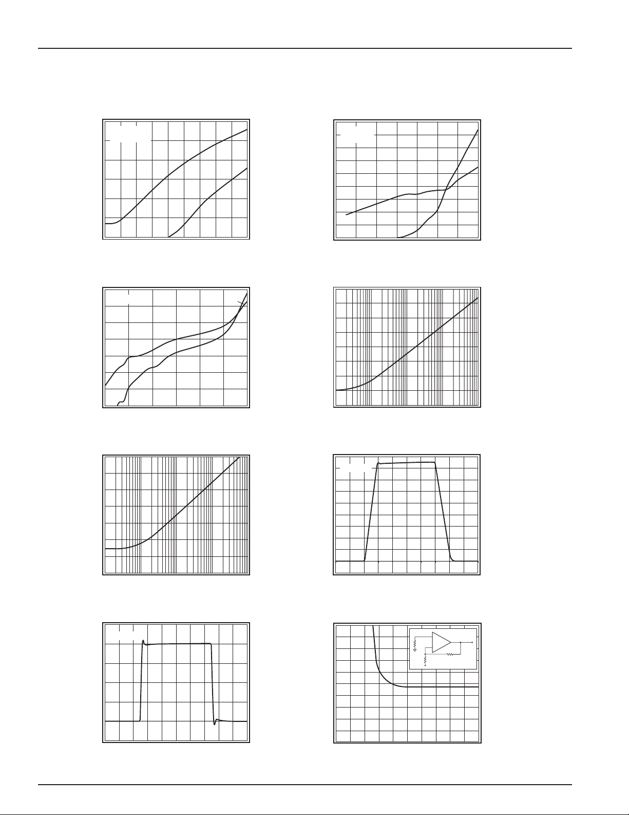
Typical Operating Characteristics
(Tc= 25°C, Vs= +2.7V, G = 2, RL= 5kΩ to Vs/2, Rf= 5kΩ, V
o (DC)
= Vcc/2; unless otherwise noted)
DATA SHEET FAN4113
6 REV. 1 October 2001
Harmonic Distortion vs. Freq., Vs = 1.2V
-60
G = -1
Vo = 500mV
-65
-70
-75
-80
Distortion (dBc)
-85
-90
100 200 300 400 500 600 700 800 900
pp
2nd
3rd
Frequency (KHz)
Harmonic Distortion vs. V
-55
f = 500kHz
-60
-65
-70
-75
-80
Distortion (dBc)
-85
-90
0.25 0.5 0.75 1 1.25 1.5
2nd
3rd
o
Output Amplitude (Vpp)
2nd
3rd
1000
1.75
Harmonic Distortion vs. Vo, Vs = 1.2V
-45
G = -1
-50
f = 500kHz
-55
-60
-65
-70
-75
Distortion (dBc)
-80
-85
-90
0.2 0.3 0.4 0.5 0.6 0.7 0.8
2nd
3rd
Output Amplitude (Vpp)
PSRR
-10
-20
-30
-40
-50
-60
PSRR (dB)
-70
-80
-90
0.1k
1k
10k
Frequency (MHz)
100k
3rd
2nd
0.9
1M
CMRR
-20
-30
-40
-50
-60
CMRR (dB)
-70
-80
-90
0.1k
1k
Frequency (Hz)
Small Signal Pulse Response
f = 500kHz
Output Voltage (0.05V/div)
Time (200µs/div)
10k
100k
Large Signal Pulse Response
f = 500kHz
Output Voltage (0.2V/div)
1M
Input Offset Voltage vs. V
5
0
Input Offset Voltage (1mV/div)
-5
0.5
Time (200µs/div)
0.8
1.1
s
+
2.5kΩ
-
5kΩ
5kΩ
1.4 1.7 2
Vs (0.15V/div)
Page 7
Application Information
General Description
The FAN4113 is single supply, general purpose, voltage-feedback
amplifier. The FAN4113 is fabricated on a complimentary bipolar
process, features a rail-to-rail output, and is unity gain stable.
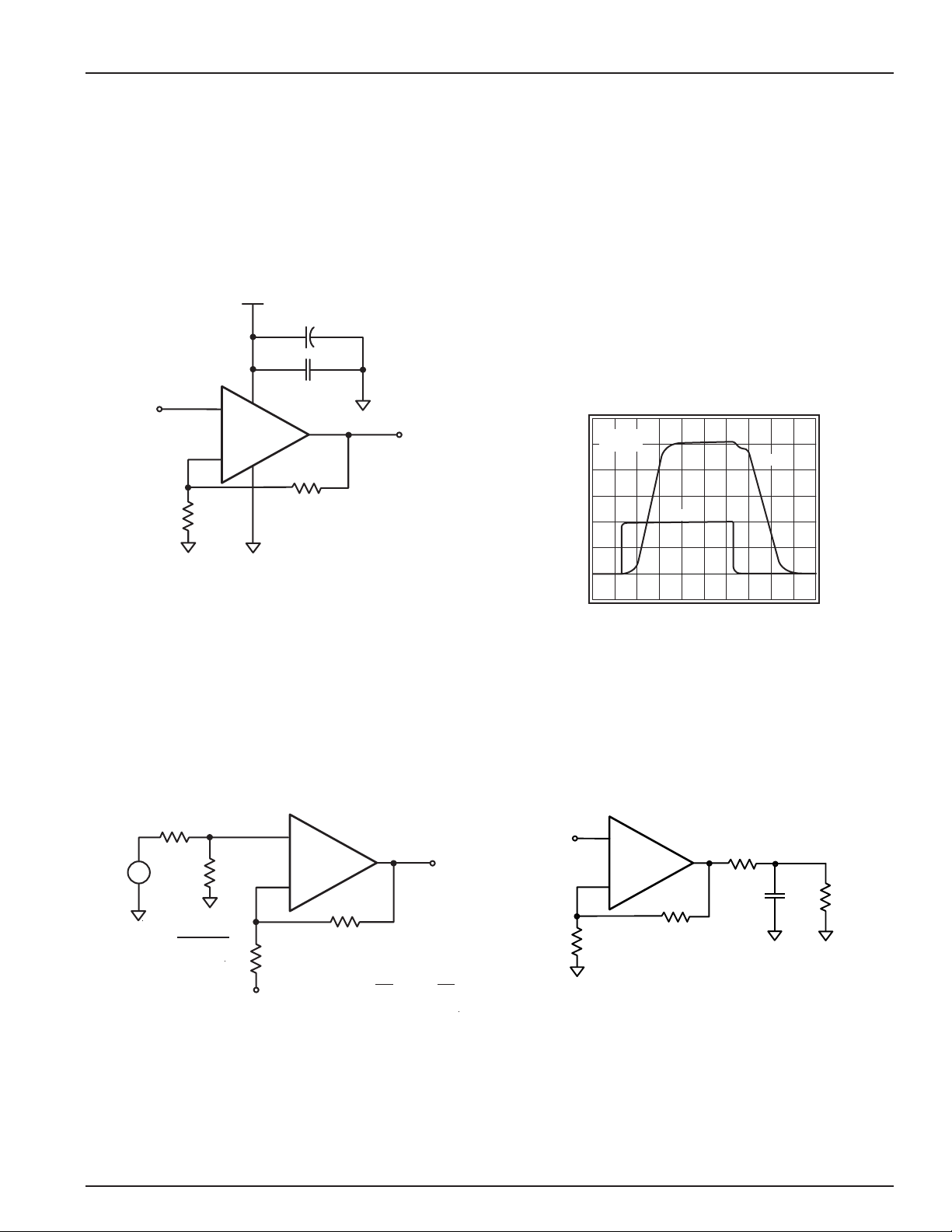
The typical non-inverting circuit schematic is shown in Figure 1.
Figure 1: Typical Non-inverting Configuration
RR Applications and Beyond
The FAN4113 can be used with input signals that exceed
its common mode input voltage range. Simply attenuate the
input signal and increase the gain of the FAN4113, see
Figure 2. First, select A1so the FAN4113 common voltage
range is not exceeded. Second, select Rfand Rgto get the
desired overall gain for signal Vin. Finally, pick VDCfor the
desired output offset.
Figure 2: RR Applications and Beyond
Power Dissipation
The maximum internal power dissipation allowed is directly
related to the maximum junction temperature. If the maximum
junction temperature exceeds 150°C, some performance
degradation will occur. It the maximum junction temperature
exceeds 175°C for an extended time, device failure may occur.
Overdrive Recovery
Overdrive of an amplifier occurs when the output and/or input
ranges are exceeded. The recovery time varies based on
whether the input or output is overdriven and by how much
the ranges are exceeded. The FAN4113 will typically recover
in less than 50ns from an overdrive condition. Figure 3
shows the FAN4113 in an overdriven condition.
Figure 3: Overdrive Recovery
Driving Capacitive Loads
The Frequency Response vs. CLplot, illustrates the response
of the FAN4113. A small series resistance (Rs) at the output
of the amplifier, illustrated in Figure 4, will improve stability
and settling performance.
Figure 4: Typical Topology for driving
a capacitive load
Output Voltage (0.5V/div)
Time (200µs/div)
G = 5V
Vs = 2.7V
Output
Input
+
R
f
R
g
R
s
C
L
R
L
FAN4113 DATA SHEET
REV. 1 October 2001 7
+V
s
6.8µF
+
In
R
g
+
FAN4113
-
0.01µF
R
f
Out
R
1
+
R
2
R1 + R
R
2
2
V
–
R
g
Vo = A1Vin1+
DC
R
f
V
in
*
A1=
V
o
R
f
R
g
R
−V
DC
f
R
g
Page 8
Layout Considerations
General layout and supply bypassing play major roles in high
frequency performance. Fairchild has evaluation boards to
use as a guide for high frequency layout and as aid in device
testing and characterization. Follow the steps below as a
basis for high frequency layout:
• Include 6.8µF and 0.01µF ceramic capacitors
• Place the 6.8µF capacitor within 0.75 inches of
the power pin
• Place the 0.01µF capacitor within 0.1 inches of
the power pin
• Remove the ground plane under and around the part,
especially near the input and output pins to reduce parasitic
capacitance
• Minimize all trace lengths to reduce series inductances
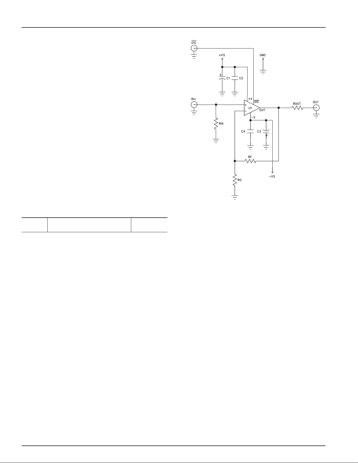
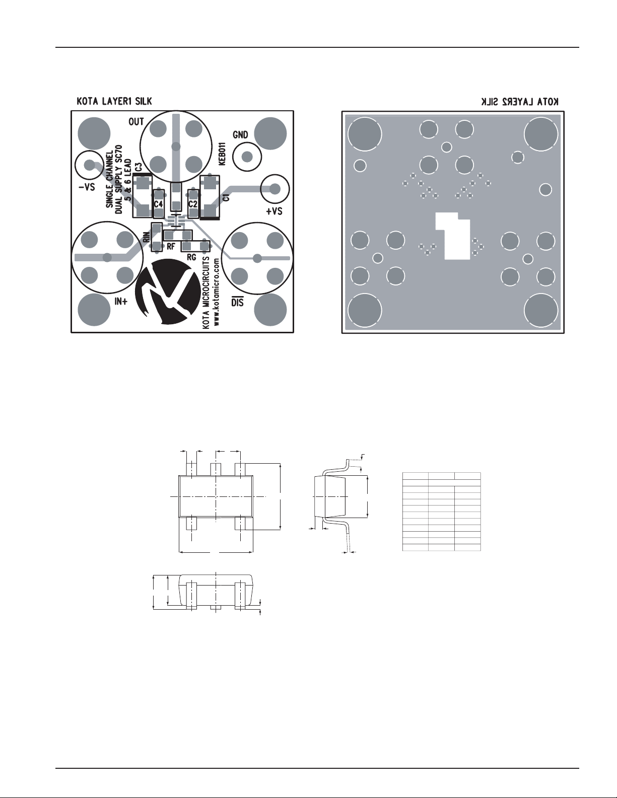
Refer to the evaluation board layouts shown in Figure 6 for
more information.
Evaluation Board Information
The following evaluation boards are available to aid in the
testing and layout of this device:
Evaluation board schematics and layouts are shown in Figure 5
and Figure 6.
Figure 5: Evaluation Board Schematic
Eval Bd Description Products
KEB011 Single Channel, Dual Supply, FAN4113IP5
5 and 6 lead SC70
DATA SHEET FAN4113
8 REV. 1 October 2001
Page 9
FAN4113 DATA SHEET
REV. 1 October 2001 9
FAN4113 Evaluation Board Layout
Figure 6a: KEB011 (top side) Figure 6b: KEB011 (bottom side)
FAN4113 Package Dimensions
SYMBOL MIN MAX
e 0.65 BSC
D 1.80 2.20
b 0.15 0.30
E 1.15 1.35
HE 1.80 2.40
Q1 0.10 0.40
A2 0.80 1.00
A1 0.00 0.10
A 0.80 1.10
c 0.10 0.18
L 1.10 0.30
b
e
D
C
L
HE
C
L
C
L
A
A2
A1
E
C
C
L
NOTE:
1. All dimensions are in millimeters.
2. Dimensions are inclusive of plating.
3. Dimensions are exclusive of mold flashing and metal burr.
4. All speccifications comply to EIAJ SC70.
L
Q1
SC70-5
Page 10

DISCLAIMER
FAIRCHILD SEMICONDUCTOR RESERVES THE RIGHT TO MAKE CHANGES WITHOUT FURTHER NOTICES TO ANY PRODUCTS HEREIN TO IMPROVE RELIABILITY, FUNCTION OR DESIGN.
FAIRCHILD DOES NOT ASSUME ANY LIABILITY ARISING OUT OF THE APPLICATION OR USE OF ANY PRODUCT OR CIRCUIT DESCRIBED HEREIN; NEITHER DOES IT CONVEY ANY
LICENSE UNDER ITS PATENT RIGHTS, NOR THE RIGHTS OF OTHERS.
LIFE SUPPORT POLICY
FAIRCHILD’S PRODUCTS ARE NOT AUTHORIZED FOR USE AS CRITICAL COMPONENTS IN LIFE SUPPORT DEVICES OR SYSTEMS WITHOUT THE EXPRESS WRITTEN APPROVAL OF THE
PRESIDENT OF FAIRCHILD SEMICONDUCTOR CORPORATION. As used herein:
1. Life support devices or systems are devices or systems which, (a) are intended for
surgical implant into the body, or (b) support or sustain life, and (c) whose failure to perform when properly used in accordance with instructions for use provided in the labeling,
can be reasonably expected to result in a significant injury of the user.
2. A critical component in any component of a life support device or system whose failure
to perform can be reasonably expected to cause the failure of the life
support device or system, or to affect its safety or effectiveness.
www.fairchildsemi.com © 2001 Fairchild Semiconductor Corporation
Ordering Information
Model Part Number Package Container Pack Qty
FAN4113 FAN4113IP5 SC70-5 Partial Reel <3000
FAN4113 FAN4113IP5X SC70-5 Reel 3000
Temperature range for all parts: -40°C to +85°C.
DATA SHEET FAN4113
 Loading...