

Page 1
November 2010
FAN4860
3MHz, Synchronous TinyBoost™ Regulator
FAN4860 — 3MHz, Synchronous TinyBoost™ Regulator
Features
Operates with Very Small External Components:
1μH Inductor and 0402 Case Size Input and Output
Capacitors
Input Voltage Range from 2.3V to 4.5V
Fixed 3.3V or 5.0V Output Voltage Options
Maximum Load Current >200mA at V
Maximum Load Current 300mA at V
Maximum Load Current 300mA at V
=2.3V
IN
=3.3V, V
IN
=2.7V, V
IN
OUT
OUT
=5V
=3.3V
Up to 92% Efficient
Low Operating Quiescent Current
True Load Disconnect During Shutdown
Variable On-time Pulse Frequency Modulation (PFM) with
Light-Load Power-Saving Mode
Internal Synchronous Rectifier
(No External Diode Needed)
Thermal Shutdown and Overload Protection
6-Pin 2 x 2mm UMLP
6-Bump WLCSP, 0.4mm Pitch
Applications
Description
The FAN4860 is a low-power boost regulator designed to
provide a regulated 3.3V or 5V output from a single cell
Lithium or Li-Ion battery. Output voltage options are fixed at
either 3.3V or 5.0V with a guaranteed maximum load current
of 200mA at V
in shut-down mode is less than 1µA, which maximizes
battery life.
Light-load PFM operation is automatic and “glitch-free”. The
regulator maintains output regulation at no-load with as low
as 37µA quiescent current.
The combination of built-in power transistors, synchronous
rectification, and low supply current make the FAN4860 ideal
for battery powered applications.
The FAN4860 is available in 6-bump 0.4mm pitch WaferLevel Chip Scale Package (WLCSP) and a 6-lead 2x2mm
ultra-thin MLP package.
=2.3V and 300mA at VIN=3.3V. Input current
IN
USB “On the Go” 5V Supply
5V Supply – HDMI, H-Bridge Motor Drivers
Powering 3.3V Core Rails
PDAs, Portable Media Players
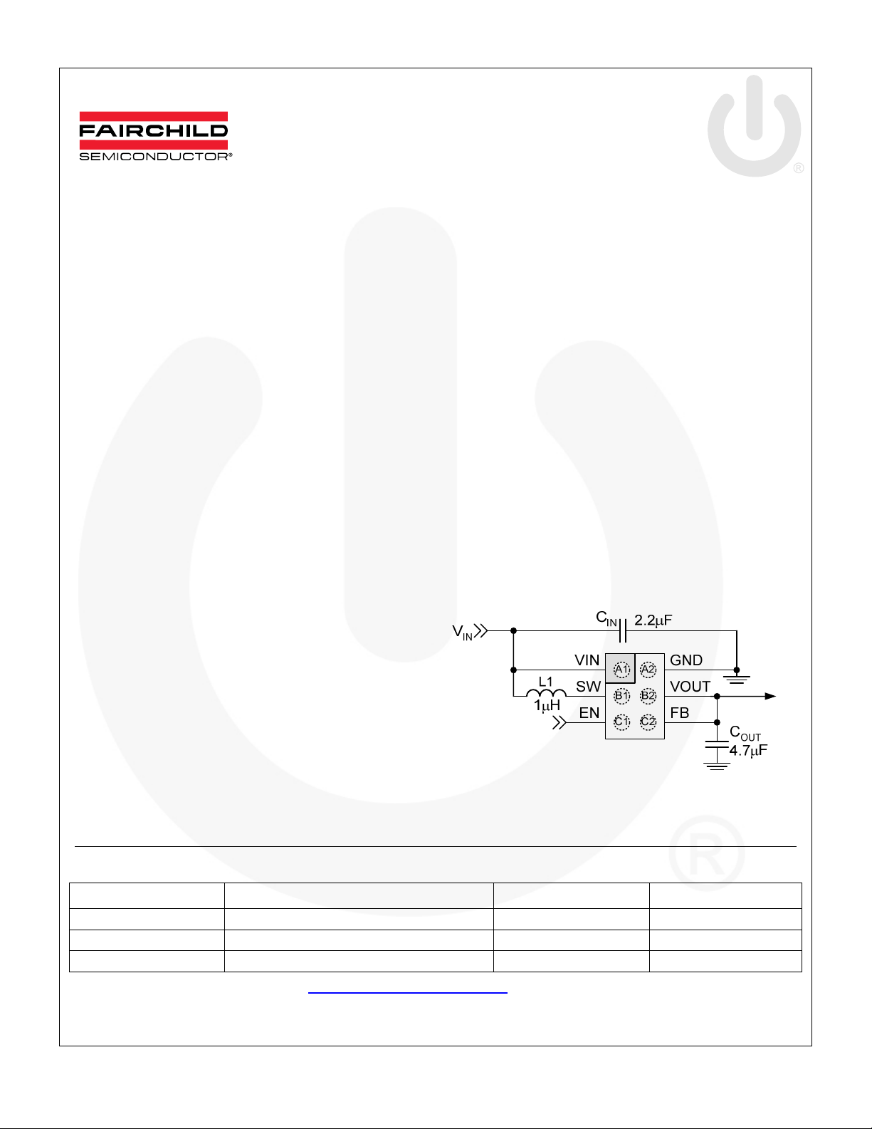
Figure 1. Typical Application
Cell Phones, Smart Phones, Portable Instruments
Ordering Information
Part Number Operating Temperature Range Package Packing Method
FAN4860UC5X -40°C to 85°C WLCSP, 0.4mm Pitch Tape and Reel
FAN4860UMP5X -40°C to 85°C UMLP-6, 2 x 2mm Tape and Reel
FAN4860UC33X -40°C to 85°C WLCSP, 0.4mm Pitch Tape and Reel
Please refer to tape and reel specifications at http://www.fairchildsemi.com/packaging.
© 2010 Fairchild Semiconductor Corporation www.fairchildsemi.com
FAN4860 • Rev. 1.1.0
Page 2
Block Diagrams
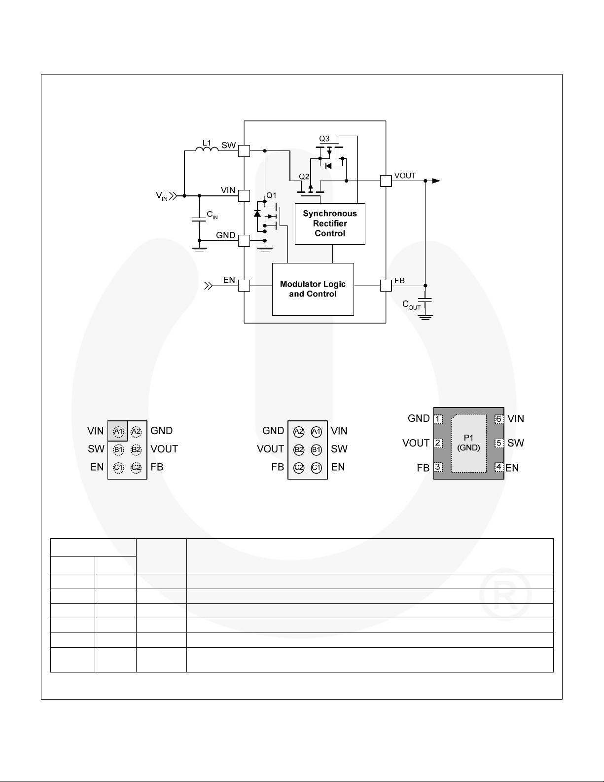
Figure 2. IC Block Diagram
FAN4860 — 3MHz, Synchronous TinyBoost™ Regulator
Pin Configuration
Figure 3. WLCSP (Top View) Figure 4. WLCSP (Bottom View) Figure 5. 2X2mm UMLP (Top View)
Pin Definitions
Pin #
WLCSP UMLP
A1 6 VIN
B1 5 SW
C1 4 EN
C2 3 FB
B2 2 VOUT
A2 1, P1 GND
Name Description
Input Voltage. Connect to Li-Ion battery input power source and input capacitor (C
Switching Node. Connect to inductor.
Enable. When this pin is HIGH, the circuit is enabled. This pin should not be left floating.
Feedback. Output voltage sense point for V
Output Voltage. This pin is both the output voltage terminal as well as an IC bias supply.
Ground. Power and signal ground reference for the IC. All voltages are measured with
respect to this pin.
. Connect to output capacitor (C
OUT
OUT
).
IN
).
© 2010 Fairchild Semiconductor Corporation www.fairchildsemi.com
FAN4860 • Rev. 1.1.0 2
Page 3
FAN4860 — 3MHz, Synchronous TinyBoost™ Regulator
Absolute Maximum Ratings
Stresses exceeding the absolute maximum ratings may damage the device. The device may not function or be operable above
the recommended operating conditions and stressing the parts to these levels is not recommended. In addition, extended
exposure to stresses above the recommended operating conditions may affect device reliability. The absolute maximum
ratings are stress ratings only.
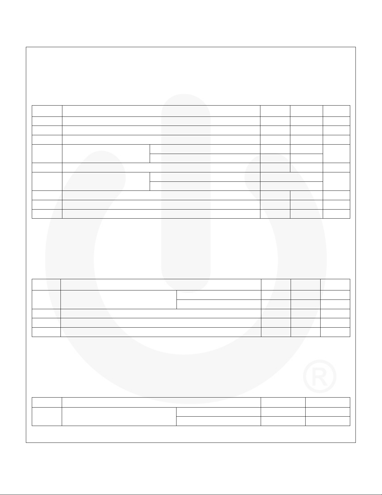
Symbol Parameter Min. Max. Units
VIN VIN Pin -0.3 5.5 V
V
VOUT Pin –2 6 V
OUT
VFB FB Pin –2 14 V
VSW SW Node
VEN EN Pin -0.3 5.5 V
ESD
TJ Junction Temperature –40 +150 °C
T
STG
TL Lead Soldering Temperature, 10 Seconds +260 °C
Electrostatic Discharge
Protection Level
Storage Temperature –65 +150 °C
DC
Transient: 10ns, 3MHz -1.0 6.5
Human Body Model per JESD22-A114 2
Charged Device Model per JESD22-C101 1
-0.3 5.5
V
kV
Recommended Operating Conditions
The Recommended Operating Conditions table defines the conditions for actual device operation. Recommended operating
conditions are specified to ensure optimal performance to the datasheet specifications. Fairchild does not recommend
exceeding them or designing to absolute maximum ratings.
Symbol Parameter Min. Max. Units
VIN Supply Voltage
I
Output Current 200 mA
OUT
TA Ambient Temperature –40 +85 °C
TJ Junction Temperature –40 +125 °C
5.0 V
3.3 V
2.3 4.5 V
OUT
2.5 3.2 V
OUT
Thermal Properties
Junction-to-ambient thermal resistance is a function of application and board layout. This data is measured with four-layer
2s2p boards in accordance to JEDEC standard JESD51. Special attention must be paid not to exceed junction temperature
at a given ambient temperate TA.
T
J(max)
Symbol Parameter Typical Units
θJA
Junction-to-Ambient Thermal Resistance
WLCSP 130 °C/W
UMLP 57 °C/W
© 2010 Fairchild Semiconductor Corporation www.fairchildsemi.com
FAN4860 • Rev. 1.1.0 3
Page 4
FAN4860 — 3MHz, Synchronous TinyBoost™ Regulator
Electrical Specifications
Minimum and maximum values are at VIN=VEN=2.3V to 4.5V (2.5 to 3.2 VIN for 3.3 V
Figure 1, unless otherwise noted. Typical values are at T
=25°C, VIN=VEN=3.6V for V
A
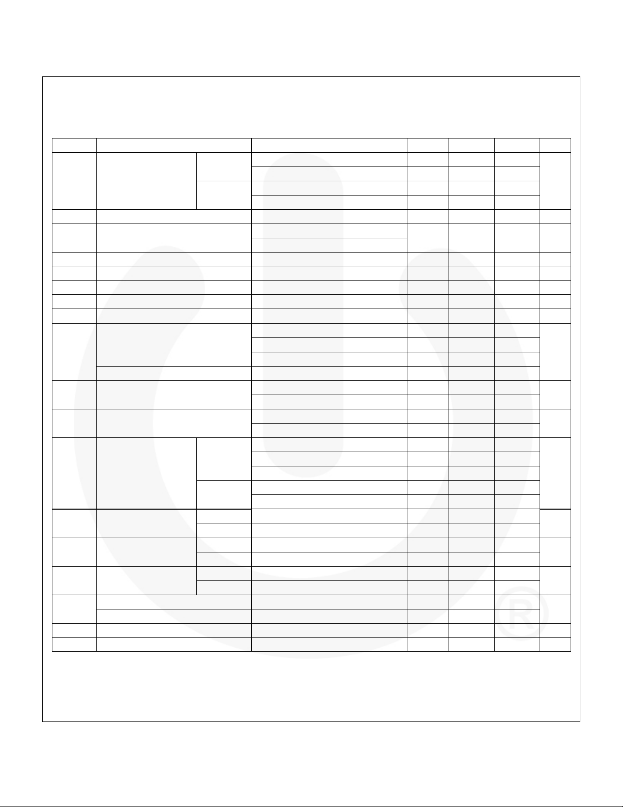
Symbol Parameter Conditions Min. Typ. Max. Units
5.0 V
OUT
IIN VIN Input Current
3.3 V
OUT
I
V
LK_OUT
I
LK_RVSR
V
Under-Voltage Lockout VIN Rising 2.2 2.3 V
UVLO
V
UVLO_HYS
V
Enable HIGH Voltage 1.05 V
ENH
V
Enable LOW Voltage 0.4 V
ENL
I
Enable Input Leakage Current 0.01 1
LK_EN
Leakage Current V
OUT
V
to VIN Reverse Leakage
OUT
Under-Voltage Lockout Hysteresis 190 mV
Quiescent: V
Shutdown: EN=0, VIN=3.6V 0.5 1.5
Quiescent: V
Shutdown: EN=0, VIN=2.7V 0.5 1.5
=0, EN=0, VIN≥3V 10 nA
OUT
V
=5V, VIN=3.6V, EN=0
OUT
V
=3.3V, VIN=3V, EN=0
OUT
VIN from 2.3V to 4.5V, I
(1)
VIN from 2.7V to 4.5V, I
VIN from 3.3V to 4.5V, I
(1)
VIN from 2.5V to 3.2V, I
Referred to V
Referred to V
=3.6V, V
V
IN
VIN=2.7V, V
V
=2.3V 200
IN
OUT
VIN=3.3V 300
VIN=3.6V 400
V
=2.5V 250
IN
OUT
OUT
OUT
OUT
OUT
OUT
OUT
VIN=2.7V 300
VIN=3.6V, V
VIN=2.7V, V
VIN=3.6V, V
VIN=2.7V, V
VIN=3.6V, I
VIN=2.7V, I
=3.6V 300
IN
=10mA 150 °C
LOAD
OUT
5.0 V
V
3.3 V
V
Reference Accuracy
REF
t
Off Time
OFF
I
OUT
Maximum Output
Current
Output Voltage Accuracy
OUT
Output Voltage Accuracy
OUT
(2)
ISW SW Peak Current Limit
ISS
tSS Soft-Start Time
R
DS(ON)
T
T
TSD_HYS
Soft-Start Input Peak
Current Limit
N-Channel Boost Switch V
P-Channel Sync Rectifier VIN=3.6V 400
Thermal Shutdown I
TSD
(2)
(3)
Thermal Shutdown Hysteresis 30 °C
5.0 V
3.3 V
5.0 V
3.3 V
5.0 V
3.3 V
5.0 V
3.3 V
=3.6V, I
IN
=2.7V, I
IN
=5V 4.975 5.050 5.125
OUT
=3.3V 3.280 3.330 3.380
OUT
=5V, I
OUT
=3.3V, I
OUT
OUT>VIN
OUT>VIN
< VIN 850
OUT
< VIN 700
OUT
=200mA 100 300
OUT
=200mA 250 750
OUT
=0, EN=V
OUT
=0, EN=V
OUT
≤200mA 4.80 5.05 5.15
OUT
≤200mA 4.85 5.05 5.15
OUT
≤300mA 4.85 5.05 5.15
OUT
≤200mA 3.17 3.33 3.41
OUT
=200mA 195 240 265
OUT
=200mA 240 290 350
OUT
930 1100 1320
650 800 950
Notes:
1. I
from 0 to I
LOAD
; also includes load transient response. V
OUT
Effective capacitance of C
> 1.5μF.
OUT
measured from mid-point of output voltage ripple.
OUT
2. Guaranteed by design and characterization; not tested in production.
3. Elapsed time from rising EN until regulated V
OUT.
option), TA=-40°C to +85°C; circuit of
OUT
=5V, and VIN=VEN=2.7V for V
OUT
37 45
IN
50 65
IN
OUT
2.5
=3.3V.
μA
μA
μA
V
V
ns
mA
mA
mA
μs
mΩ
© 2010 Fairchild Semiconductor Corporation www.fairchildsemi.com
FAN4860 • Rev. 1.1.0 4
Page 5
FAN4860 — 3MHz, Synchronous TinyBoost™ Regulator
5.0 V
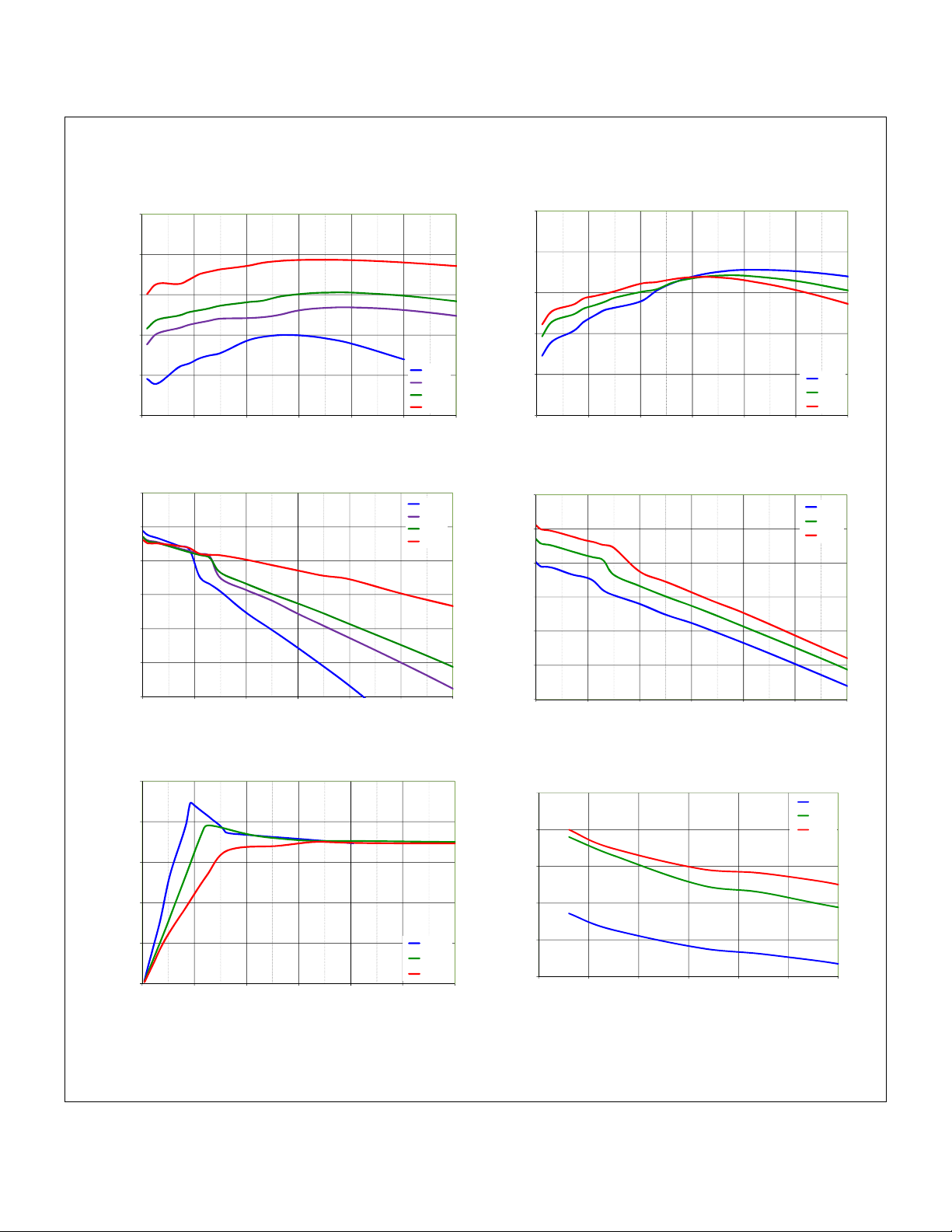
Typical Characteristics
OUT
Unless otherwise specified, circuit per Figure 1, 3.6VIN, TA=25°C.
100
95
90
85
Efficiency (%)
80
75
0 50 100 150 200 250 300
Load Current (mA)
2.5 Vin
3.3 Vin
3.6 Vin
4.5 Vin
Figure 6. Efficiency vs. VIN Figure 7. Efficiency vs. Temperature, 3.6VIN
50
25
0
-25
2.5 Vin
3.3 Vin
3.6 Vin
4.5 Vin
95
92
89
Efficiency (%)
86
83
80
0 50 100 150 200 250 300
Load Current (mA)
50
25
0
-25
-40C
+25C
+85C
-40C
+25C
+85C
-50
VOUT - 5.05V (mV)
-75
-100
0 50 100 150 200 250 300
Load Current (mA)
Figure 8. Line and Load Regulation Figure 9. Load Regulation vs. Temperature, 3.6V
4000
3200
2400
1600
Frequency (KHz)
800
0
0 50 100 150 200 250 300
Load Current (mA)
Figure 10. Switching Frequency Figure 11. Quiescent Current
2.5 Vin
3.6 Vin
4.5 Vin
-50
VOUT - 5.05V (mV)
-75
-100
0 50 100 150 200 250 300
Load Current (mA)
IN
50
45
40
35
Quiescent Current (uA)
30
25
2.0 2.5 3.0 3.5 4.0 4.5 5.0
Input Voltage(V)
-40C
+25C
+85C
© 2010 Fairchild Semiconductor Corporation www.fairchildsemi.com
FAN4860 • Rev. 1.1.0 5
Page 6
FAN4860 — 3MHz, Synchronous TinyBoost™ Regulator
5.0 V
Unless otherwise specified, circuit per Figure 1, 3.6VIN, TA=25°C.
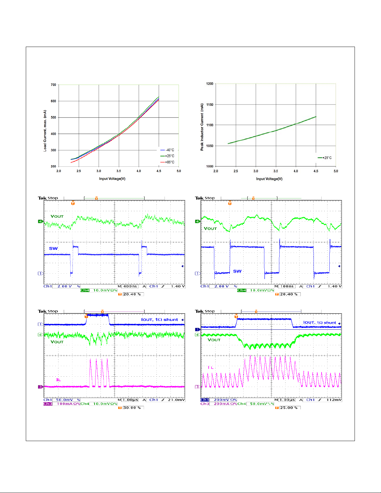
Typical Characteristics
OUT
Figure 12. Maximum DC Load Current Figure 13. Peak Inductor Current
Figure 14. Output Ripple, 10mA PFM Load Figure 15. Output Ripple, 200mA PWM Load
Figure 16. 0-50mA Load Transient, 100ns Step Figure 17. 50-200mA Load Transient, 100ns Step
© 2010 Fairchild Semiconductor Corporation www.fairchildsemi.com
FAN4860 • Rev. 1.1.0 6
Page 7
FAN4860 — 3MHz, Synchronous TinyBoost™ Regulator
5.0 V
Unless otherwise specified, circuit per Figure 1, 3.6VIN, TA=25°C.
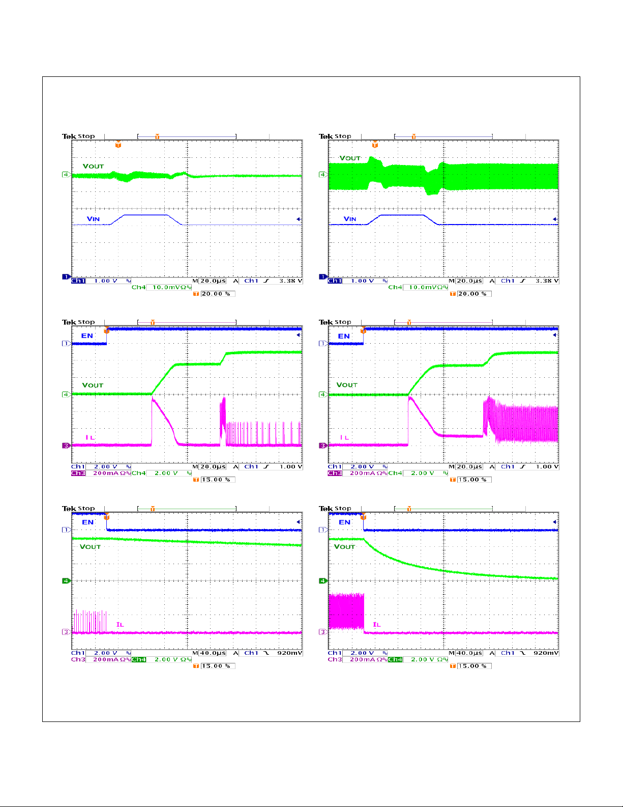
Typical Characteristics
OUT
Figure 18. Line Transient, 5mA Load, 10µs Step Figure 19. Line Transient, 200mA Load, 10µs Step
Figure 20. Startup, No Load
Figure 22. Shutdown, 1KΩ Load Figure 23. Shutdown, 33Ω Load
© 2010 Fairchild Semiconductor Corporation www.fairchildsemi.com
FAN4860 • Rev. 1.1.0 7
Figure 21. Startup, 33Ω Load
Page 8
FAN4860 — 3MHz, Synchronous TinyBoost™ Regulator
5.0 V
Unless otherwise specified, circuit per Figure 1, 3.6VIN, TA=25°C.
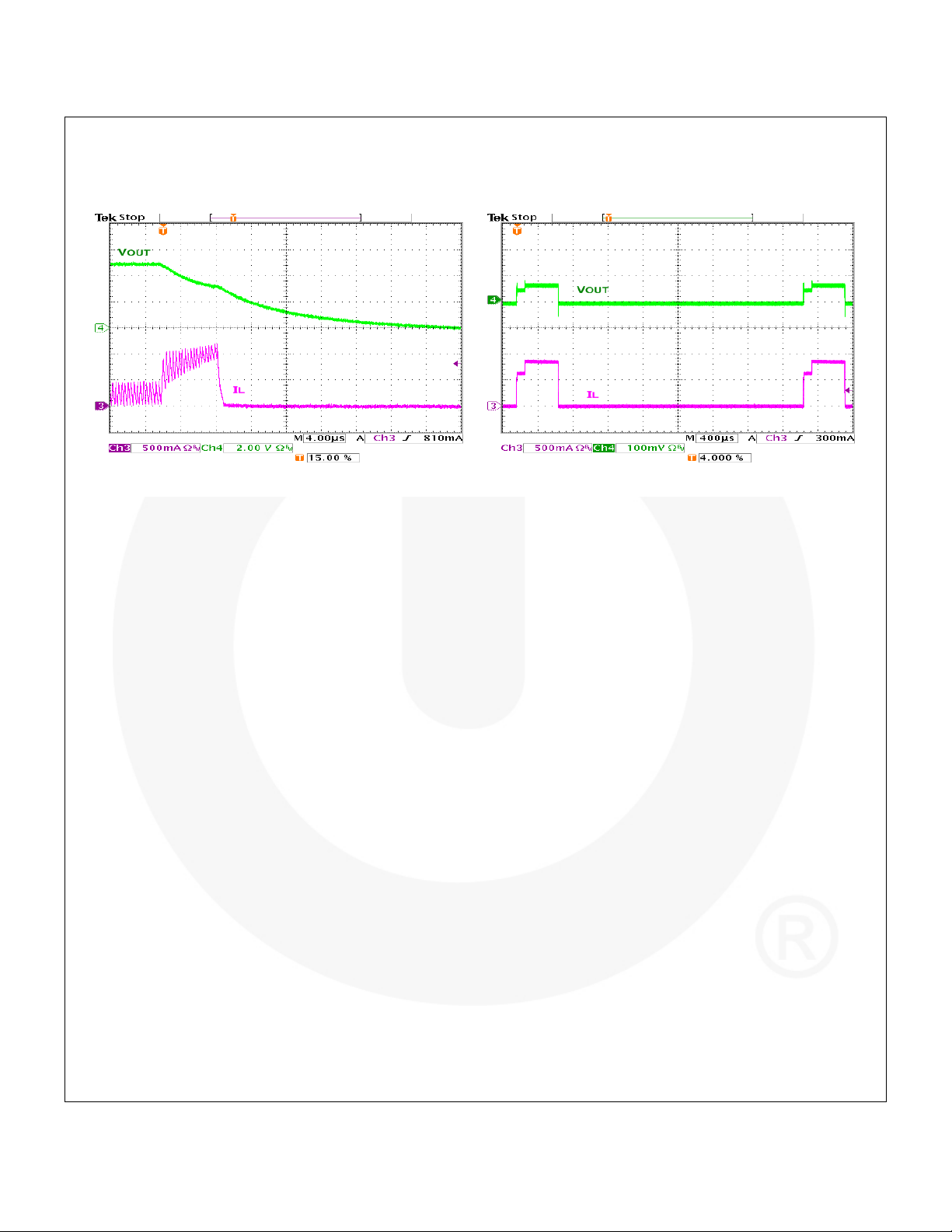
Typical Characteristics
OUT
Figure 24. Overload Protection Figure 25. Short-Circuit Response
© 2010 Fairchild Semiconductor Corporation www.fairchildsemi.com
FAN4860 • Rev. 1.1.0 8
Page 9
FAN4860 — 3MHz, Synchronous TinyBoost™ Regulator
3.3 V
Typical Characteristics
OUT
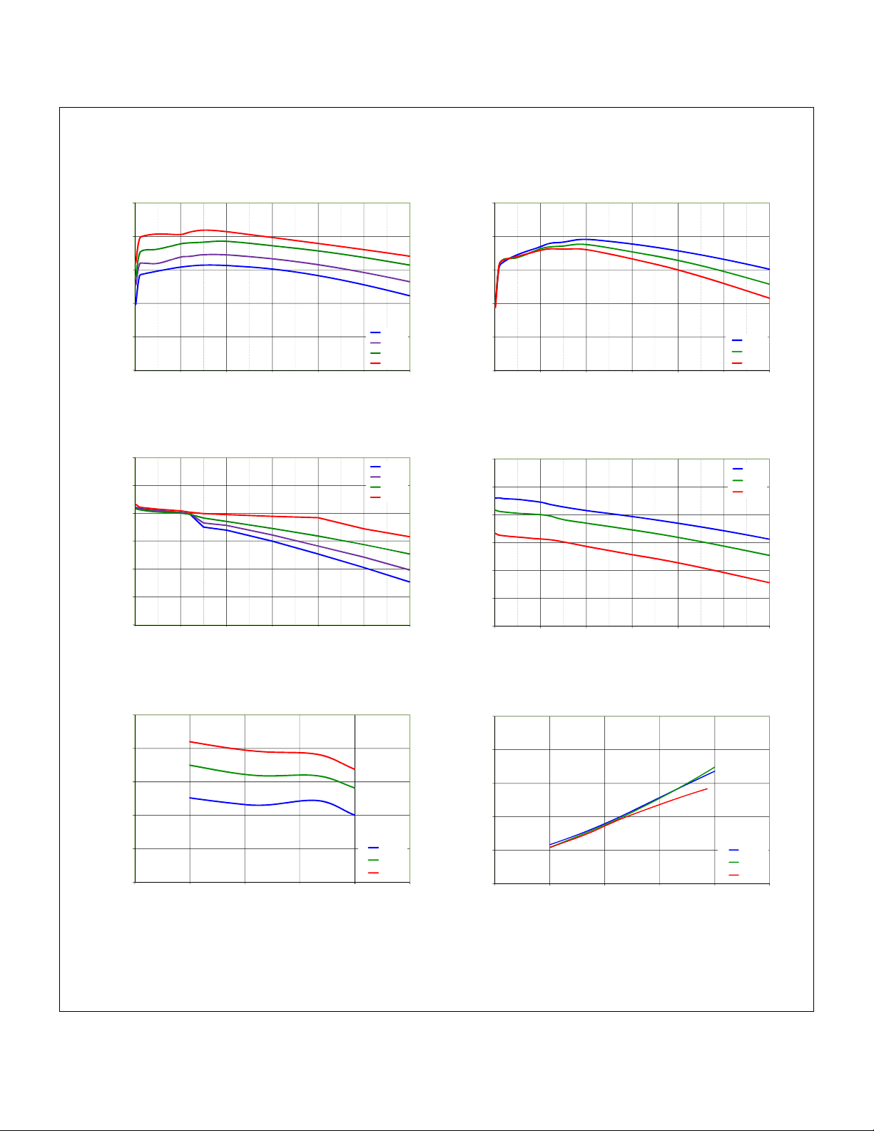
Unless otherwise specified, circuit per Figure 1, 3.0VIN, TA=25°C.
100
95
90
85
Efficiency (%)
80
75
0 50 100 150 200 250 300
Load Current (mA)
2.5 Vin
2.7 Vin
3.0 Vin
3.2 Vin
Figure 26. Efficiency vs. VIN Figure 27. Efficiency vs. Temperature, 3.0VIN
40
20
0
-20
2.5 Vin
2.7 Vin
3.0 Vin
3.2 Vin
98
95
92
89
Efficiency (%)
86
83
0 50 100 150 200 250 300
Load Current (mA)
40
20
0
-20
-40C
+25C
+85C
-40C
+25C
+85C
-40
VOUT - 3.33V (mV)
-60
-80
0 50 100 150 200 250 300
Load Current (mA)
Figure 28. Line and Load Regulation Figure 29. Load Regulation vs. Temperature, 3.0V
55
50
45
40
Quiescent Current (uA)
35
30
2.0 2.3 2.6 2.9 3.2 3.5
Input Voltage(V)
Figure 30. Quiescent Current Figure 31. Maximum DC Load Current
-40C
+25C
+85C
-40
VOUT - 3.33V (mV)
-60
-80
0 50 100 150 200 250 300
Load Current (mA)
700
600
500
400
300
Maximum DC Load Current (mA)
200
2.0 2.3 2.6 2.9 3.2 3.5
Input V ol tage(V)
IN
-40C
+25C
+85C
© 2010 Fairchild Semiconductor Corporation www.fairchildsemi.com
FAN4860 • Rev. 1.1.0 9
Page 10
FAN4860 — 3MHz, Synchronous TinyBoost™ Regulator
3.3 V
Unless otherwise specified, circuit per Figure 1, 3.0VIN, TA=25°C.
Typical Characteristics
OUT
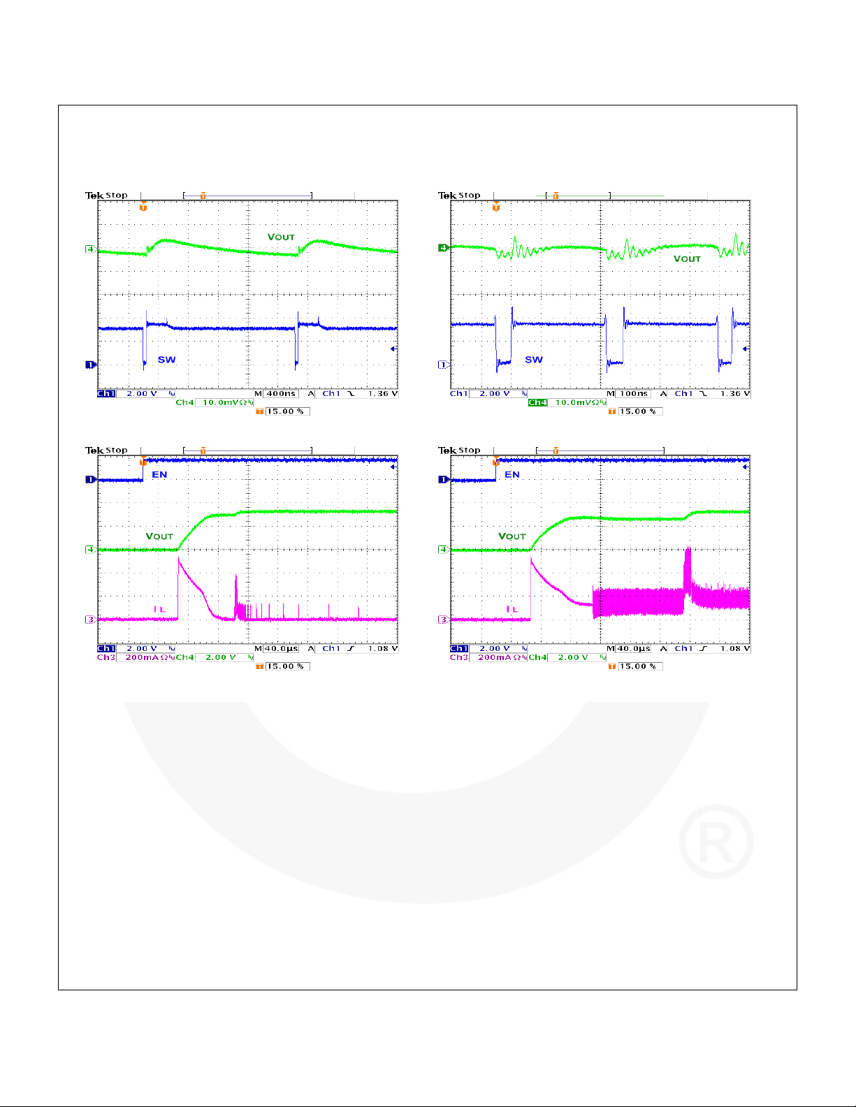
Figure 32. Output Ripple, 10mA PFM Load Figure 33. Output Ripple, 200mA PWM Load
Figure 34. Startup, No Load
Figure 35. Startup, 22Ω Load
© 2010 Fairchild Semiconductor Corporation www.fairchildsemi.com
FAN4860 • Rev. 1.1.0 10
Page 11
Functional Description
FAN4860 — 3MHz, Synchronous TinyBoost™ Regulator
Circuit Description
FAN4860 is a synchronous boost regulator, typically operating
at 3MHz in continuous conduction mode (CCM), which occurs
at moderate to heavy load current and low V
voltages.
IN
At light-load currents, the converter switches automatically to
power-saving PFM mode. The regulator automatically and
smoothly transitions between quasi-fixed-frequency
continuous conduction PWM mode and variable-frequency
PFM mode to maintain the highest possible efficiency over
the full range of load current and input voltage.
PWM Mode Regulation
The FAN4860 uses a minimum on-time and computed
minimum off-time to regulate V
excellent transient response by employing current mode
modulation. This technique causes the regulator output to
exhibit a load line. During PWM mode, the output voltage
drops slightly as the input current rises. With a constant V
this appears as a constant output resistance.
The “droop” caused by the output resistance when a load is
applied allows the regulator to respond smoothly to load
transients with negligible overshoot.
700
600
500
400
300
Output Resistance (mΩ)
200
100
2.0 2.5 3.0 3.5 4.0 4.5 5.0
Input Voltage (V )
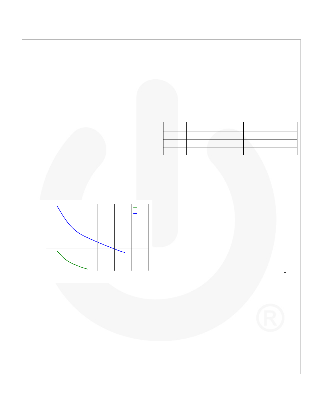
Figure 36. Output Resistance (
as a function of I
V
OUT
LOAD
regulator is in PWM mode (continuous conduction) as:
IR05.5V •−=
LOADOUTOUT
For example, at VIN=3.3V, and I
drop to:
=200mA, V
LOAD
=•−=
=•−=
OUT
At V
OUT
IN
=2.3V, and I
. The regulator achieves
OUT
IN
3.3 Vout
5.0 Vout
)
ROUT
can be computed when the
(1)
=200mA, V
LOAD
V974.42.038.005.5V
would drop to:
OUT
V914.42.068.005.5V
would
OUT
(1A)
(1B)
,
PFM Mode
If V
> V
OUT
regulator enters PFM mode. Boost pulses are inhibited until
< V
V
OUT
the output to pump up sufficiently with each PFM boost
pulse. Therefore, the regulator behaves like a constant ontime regulator, with the bottom of its output voltage ripple at
5.05V in PFM mode.
Table 1. Operating States
Mode Description Invoked When:
LIN Linear Startup VIN > V
SS Boost Soft-Start V
BST Boost Operating Mode V
Shutdown and Startup
If EN is LOW, all bias circuits are off and the regulator is in
shutdown mode. During shutdown, true load disconnect
between battery and load prevents current flow from V
, as well as reverse flow from V
V
OUT
LIN State
When EN rises, if VIN > UVLO, the regulator first attempts to
bring V
OUT
current source from VIN (I
630mA during LIN1 mode.
If V
reaches VIN-1V during LIN1 mode, the SS state is
OUT
initiated. Otherwise, LIN1 times out after 16 CLK counts and
the LIN2 mode is entered.
In LIN2 mode, the current source is incremented to 850mA.
fails to reach VIN-1V after 64 CLK counts, a fault
If V
OUT
condition is declared.
SS State
Upon the successful completion of the LIN state (V
1V), the regulator begins switching with boost pulses current
limited to about 50% of nominal level, incrementing to full
scale over a period of 32 CLK counts.
If the output fails to achieve 90% of its setpoint within 96 CLK
counts at full-scale current limit, a fault condition is declared.
BST State
This is the normal operating mode of the regulator. The
regulator uses a minimum t
scheme. Minimum t
the regulator’s switching frequency reasonably constant in
CCM. t
ON(MIN)
current reaches 0 before t
To ensure that V
regulation point, the boost switch remains off as long as
FB > V
REF
when the minimum off-time has ended, the
REF
. The minimum on-time is increased to enable
REF
OUT
< V
REG
IN
OUT
OUT
OUT=VREG
to VIN.
within about 1V of VIN by using the internal fixed
). The current is limited to about
LIN1
OUT>VIN
-minimum tON modulation
OFF
is proportional to , which keeps
OFF
V
V
IN
OUT
is proportional to VIN and is higher if the inductor
during the prior cycle.
OFF(MIN)
does not pump significantly above the
OUT
.
to
-
© 2010 Fairchild Semiconductor Corporation www.fairchildsemi.com
FAN4860 • Rev. 1.1.0 11
Page 12
Fault State
The regulator enters the FAULT state under any of the
following conditions:
V
fails to achieve the voltage required to advance from
OUT
LIN state to SS state.
V
fails to achieve the voltage required to advance from
OUT
SS state to BST state.
Sustained (32 CLK counts) pulse-by-pulse current limit
during the BST state.
The regulator moves from BST to LIN state due to a short
circuit or output overload (V
Once a fault is triggered, the regulator stops switching and
presents a high-impedance path between V
waiting 480 CLK counts, a re-start is attempted.
Soft-Start and Fault Timing
The soft-start timing for each state, and the fault times, are
determined by the fault clock, whose period is inversely
proportional to V
charge larger values of C
, this also reduces power delivered to V
V
IN
cycle in current limit.
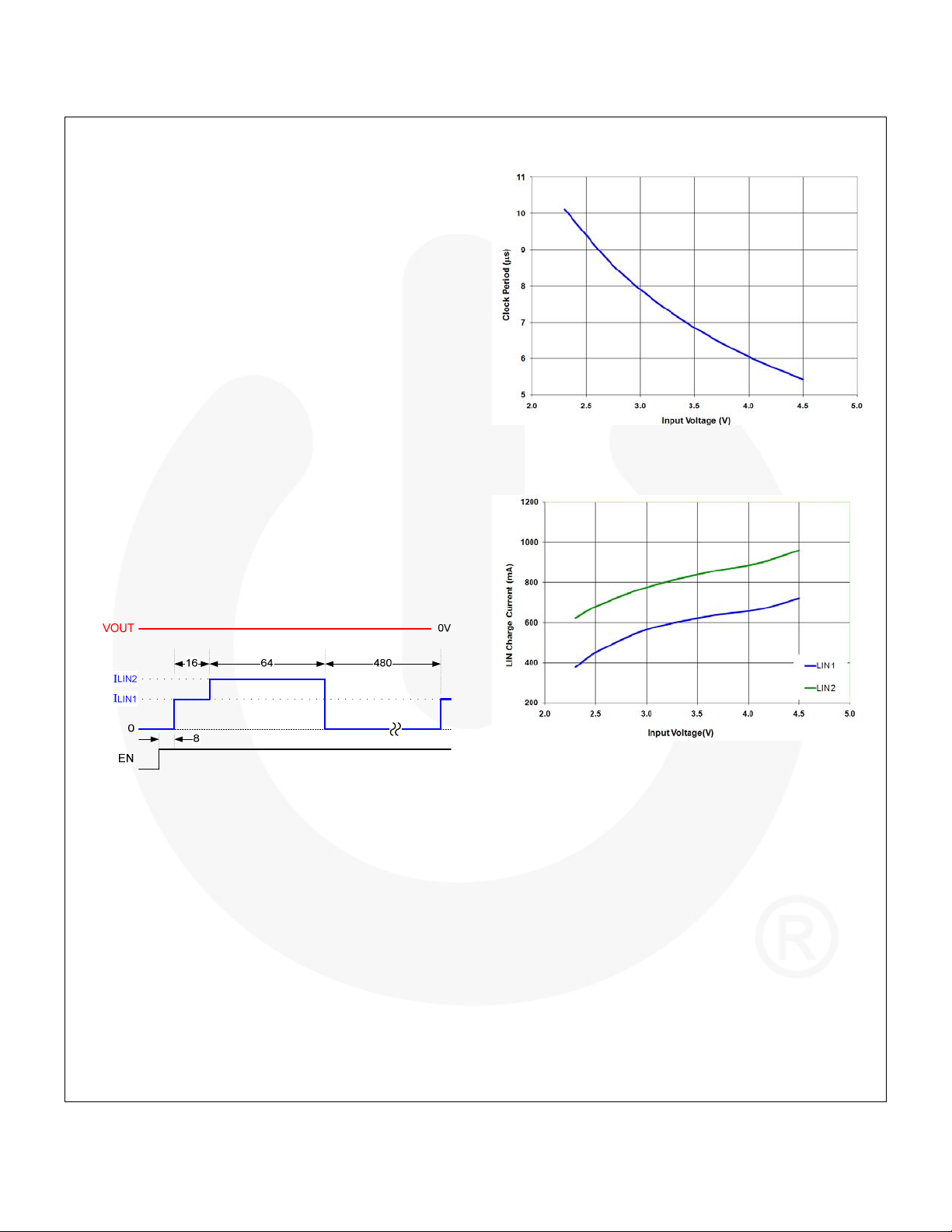
The number of clock counts for each state is illustrated in
Figure 37.
. This allows the regulator more time to
IN
< VIN-1V).
OUT
and V
IN
when VIN is lower. With higher
OUT
OUT
during each
OUT
. After
The fault clock period as a function of V
Figure 38. Fault Clock Period vs. VIN
The V
-dependent LIN mode charging current is illustrated
IN
in Figure 39.
is shown in Figure 38.
IN
FAN4860 — 3MHz, Synchronous TinyBoost™ Regulator
Figure 39. LIN Mode Current vs. V
IN
Figure 37. Fault Response into Short Circuit
Over-Temperature Protection (OTP)
The regulator shuts down when the thermal shutdown
threshold is reached. Restart, with soft-start, occurs when
the IC has cooled by about 30°C.
Over-Current Protection (OCP)
During boost-mode operation, the FAN4860 employs a
cycle-by-cycle peak current limit to protect switching
elements. Sustained current limit, for 32 consecutive fault
CLK counts, initiates a fault condition.
During an overload condition, as V
approximately V
-1V, the synchronous rectifier is
IN
immediately switched off and a fault condition is declared.
Automatic restart occurs once the overload/short is removed
and the fault timer completes counting.
© 2010 Fairchild Semiconductor Corporation www.fairchildsemi.com
FAN4860 • Rev. 1.1.0 12
collapses to
OUT
Page 13
Application Information
FAN4860 — 3MHz, Synchronous TinyBoost™ Regulator
External Component Selection
Table 2 shows the recommended external components for
the FAN4860:
Table 2. External Components
REF Description Manufacturer
1.0µH, 0.8A, 190mΩ,
L1
0805
2.2µF, 6.3V, X5R,
CIN
0402
4.7µF, 10V, X5R,
C
0603
(4)
OUT
Note:
4. A 6.3V-rated 0603 capacitor may be used for C
such as Murata GRM188R60J225M. All datasheet
parameters are valid with the 6.3V-rated capacitor.
Due to DC bias effects, the 10V capacitor offers a
performance enhancement; particularly output ripple
and transient response, without any size increase.
Output Capacitance (C
Stability
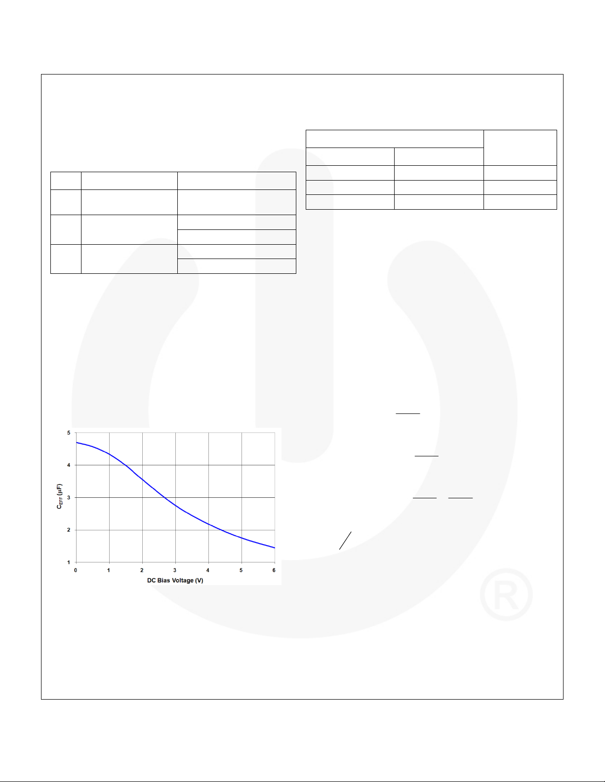
The effective capacitance (C
ceramic capacitors decrease as their bias voltage increases,
as shown in Figure 40.
Figure 40. C
FAN4860 is guaranteed for stable operation with the
minimum value of C
for 4.7μF, 0603, X5R, 6.3V (Murata
EFF
(C
EFF
Murata LQM21PN1R0MC0,
or equivalent
Murata GRM155R60J225M
TDK C1005X5R0J225M
Kemet C0603C475K8PAC
TDK C1608X5R1A475K
)
OUT
) of small, high-value,
EFF
GRM188R60J475K)
) outlined in Table 3.
EFF(MIN)
OUT
,
Table 3. Minimum C
Required for Stability
EFF
Operating Conditions
C
VIN (V) I
LOAD
(mA)
EFF(MIN)
2.3 to 4.5 0 to 200 1.5
2.7 to 4.5 0 to 200 1.0
2.3 to 4.5 0 to 150 1.0
C
varies with manufacturer, dielectric material, case size,
EFF
and temperature. Some manufacturers may be able to
provide an X5R capacitor in 0402 case size that retains C
>1.5μF with 5V bias; others may not. If this C
EFF
economically obtained and 0402 case size is required, the IC
can work with the 0402 capacitor as long as the minimum V
is restricted to >2.7V.
For best performance, a 10V-rated 0603 output capacitor is
recommended (Kemet C0603C475K8PAC, or equivalent).
Since it retains greater C
under bias and over
EFF
temperature, ouptut ripple can is reduced and transient
capability enhanced.
(μF)
EFF
cannot be
IN
Output Voltage Ripple
Output voltage ripple is inversely proportional to C
During t
supplied by C
and
Therefore:
, when the boost switch is on, all load current is
ON
.
OUT
I
LOAD
tV •=
ON)PP(RIPPLE
−
SWSWON
−
SW)PP(RIPPLE
C
OUT
⎛
V
IN
⎜
−•=•=
1tDtt
⎜
V
OUT
⎝
⎛
V
IN
⎜
1tV •
−•=
⎜
V
OUT
⎝
⎞
⎟
⎟
⎠
⎞
I
LOAD
⎟
⎟
⎠
C
OUT
where:
1
t =
SW
f
SW
As can be seen from Equation 4, the maximum V
occurs when V
is minimum and I
IN
is maximum.
LOAD
OUT
(2)
(3)
(4)
(5)
RIPPLE
.
Startup
Input current limiting is in effect during soft-start, which limits
the current available to charge C
achieve regulation within the time period described in the
soft-start section above; a FAULT occurs, causing the circuit
to shut down, then restart after a significant time period. If
is a very high value, the circuit may not start on the first
C
OUT
attempt, but eventually achieves regulation if no load is
present. If a high-current load and high capacitance are both
present during soft-start, the circuit may fail to achieve
. If the output fails to
OUT
© 2010 Fairchild Semiconductor Corporation www.fairchildsemi.com
FAN4860 • Rev. 1.1.0 13
Page 14
regulation and continually attempt soft-start, only to have
discharged by the load when in the FAULT state.
C
OUT
The circuit can start with higher values of C
under full
OUT
load if VIN is higher, since:
⎛
II •
⎜
⎝
I
−=
)PK(LIMOUT
2
V
⎞
INRIPPLE
V
OUT
(
6)
⎟
⎠
Generally, the limitation occurs in BST mode.
The FAN4860 starts on the first pass (without triggering a
FAULT) under the following conditions for C
Table 4. Maximum C
for First-Pass Startup
EFF
EFF(MAX)
:
Operating Conditions
VIN (V)
5.0 V
R
LOAD(MIN)
3.3 V
OUT
OUT
C
EFF(MAX)
> 2.3 25Ω 16Ω 10
> 2.7 25Ω 16Ω 15
> 2.7 33Ω 20Ω 22
C
values shown in Table 4 typically apply to the lowest
EFF
. The presence of higher VIN enhances ability to start into
V
IN
larger C
at full load.
EFF
(μF)
C
may be necessary to preserve load transient response
OUT2
when the Schottky is used. When a load is applied at the FB
pin, the forward voltage of the D1 rapidly increases before
the regulator can respond or the inductor current can
change. This causes an immediate drop of up to 300mV,
depending on D1’s characteristics if C
is absent. C
OUT2
supplies instantaneous current to the load while the regulator
adjusts the inductor current. A value of at least half of the
minimum value of C
should be used for C
OUT
OUT2
. C
needs to withstand the maximum voltage at the FB pin as
the TVS is clamping.
The maximum DC output current available is reduced with
this circuit, due to the additional dissipation of D1.
Layout Guideline
OUT2
OUT2
FAN4860 — 3MHz, Synchronous TinyBoost™ Regulator
Transient Protection
To protect against external voltage transients caused by
ESD discharge events, or improper external connections,
some applications employ an external transient voltage
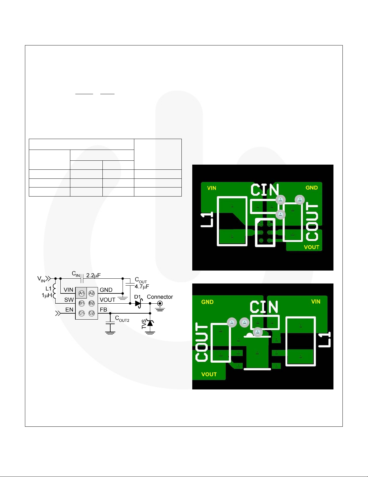
suppressor (TVS) and Schottky diode (D1 in Figure 41).
Figure 41. FAN4860 with External Transient
Protection
The TVS is designed to clamp the FB line (system V
+10V or –2V during external transient events. The Schottky
diode protects the output devices from the positive
excursion. The FB pin can tolerate up to 14V of positive
excursion, while both the FB and VOUT pins can tolerate
negative voltages.
The FAN4860 includes a circuit to detect a missing or
defective D1 by comparing V
to FB. If V
OUT
– FB > about
OUT
0.7V, the IC shuts down. The IC remains shut down until
< UVLO and VIN < UVLO+0.7 or EN is toggled.
V
OUT
OUT
) to
Figure 42. WLCSP Suggested Layout (Top View)
Figure 43. UMLP Suggested Layout (Top View)
© 2010 Fairchild Semiconductor Corporation www.fairchildsemi.com
FAN4860 • Rev. 1.1.0 14
Page 15
Physical Dimensions
FAN4860 — 3MHz, Synchronous TinyBoost™ Regulator
2X
BALL A1
INDEX AREA
0.05 C
C
0.03
F
C
E
TOP VIEW
0.40
0.40
2
1
BOTTOM VIEW
A
B
D
F
0.03
C
2X
A1
0.40
RECOMMENDED LAND PATTERN
(NSMD PAD TYPE)
0.06 C
0.625
E
0.547
SEATING PLANE
D
0.378±0.018
SIDE VIEWS
Ø0.260±0.010
6X
C
(Y) +/-0.018
B
A
(X) +/-0.018
0.005 CAB
F
NOTES:
A. NO JEDEC REGISTRATION APPLIES.
B. DIMENSIONS ARE IN MILLIMETERS.
C. DIMENSIONS AND TOLERANCES PER
ASMEY14.5M, 1994.
D. DATUM C, THE SEATING PLANE IS DEFINED
BY THE SPHERICAL CROWNS OF THE BALLS.
E. PACKAGE TYPICAL HEIGHT IS 586 MICRONS
±39 MICRONS (547-625 MICRONS).
F. FOR DIMENSIONS D, E, X, AND Y SEE
PRODUCT DATASHEET.
G. DRAWING FILENAME: UC006ACrev4.
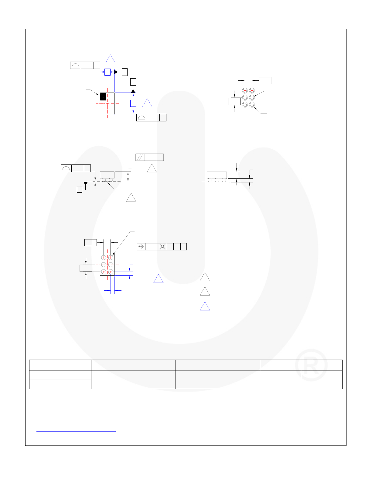
Figure 44. 6-Lead, 0.4mm Pitch, WLCSP Package
0.40
(Ø0.20)
Cu Pad
(Ø0.30)
Solder Mask
Opening
0.208±0.021
Product-Specific Dimensions
Product D E X Y
FAN4860UC5X
FAN4860UC33X
Package drawings are provided as a service to customers considering Fairchild components. Drawings may change in any manner without
notice. Please note the revision and/or date on the drawing and contact a Fairchild Semiconductor representative to verify or obtain the most
recent revision. Package specifications do not expand the terms of Fairchild’s worldwide terms and conditions, specifically the warranty therein, which
covers Fairchild products.
Always visit Fairchild Semiconductor’s online packaging area for the most recent package drawings:
http://www.fairchildsemi.com/packaging/
© 2010 Fairchild Semiconductor Corporation www.fairchildsemi.com
FAN4860 • Rev. 1.
1.0 15
1.230mm +/-0.030mm 0.880mm +/-0.030mm 0.240mm 0.215mm
.
Page 16
Physical Dimensions
FAN4860 — 3MHz, Synchronous TinyBoost™ Regulator
2X
IDENT
0.10 C
0.08
0.10 C
PIN1
C
0.05
0.00
SEATING
PLANE
2.0
TOP VIEW
0.55 MAX
SIDE VIEW
A
B
1.45
2.0
0.10
C
(0.25)
0.80
1.80
2X
0.50
6X
0.35
6X
A
(0.15)
RECOMMENDED LAND PATTERN
C
0.65
NOTES:
A. PACKAGE CONFORMS TO JEDEC MO-229
EXCEPT WHERE NOTED.
B. DIMENSIONS ARE IN MILLIMETERS.
C. DIMENSIONS AND TOLERANCES PER
ASME Y14.5M, 1994.
D. LANDPATTERN RECOMMENDATION IS BASED
ON FSC DESIGN ONLY.
E. DRAWING FILENAME: MKT-UMLP06Erev2.
0.10 C A B
0.05 C
PIN1
IDENT
0.35
6X
0.25
6X
0.35
0.25
1.35
1.45
1
6
3
0.70
0.80
4
0.65
BOTTOM VIEW
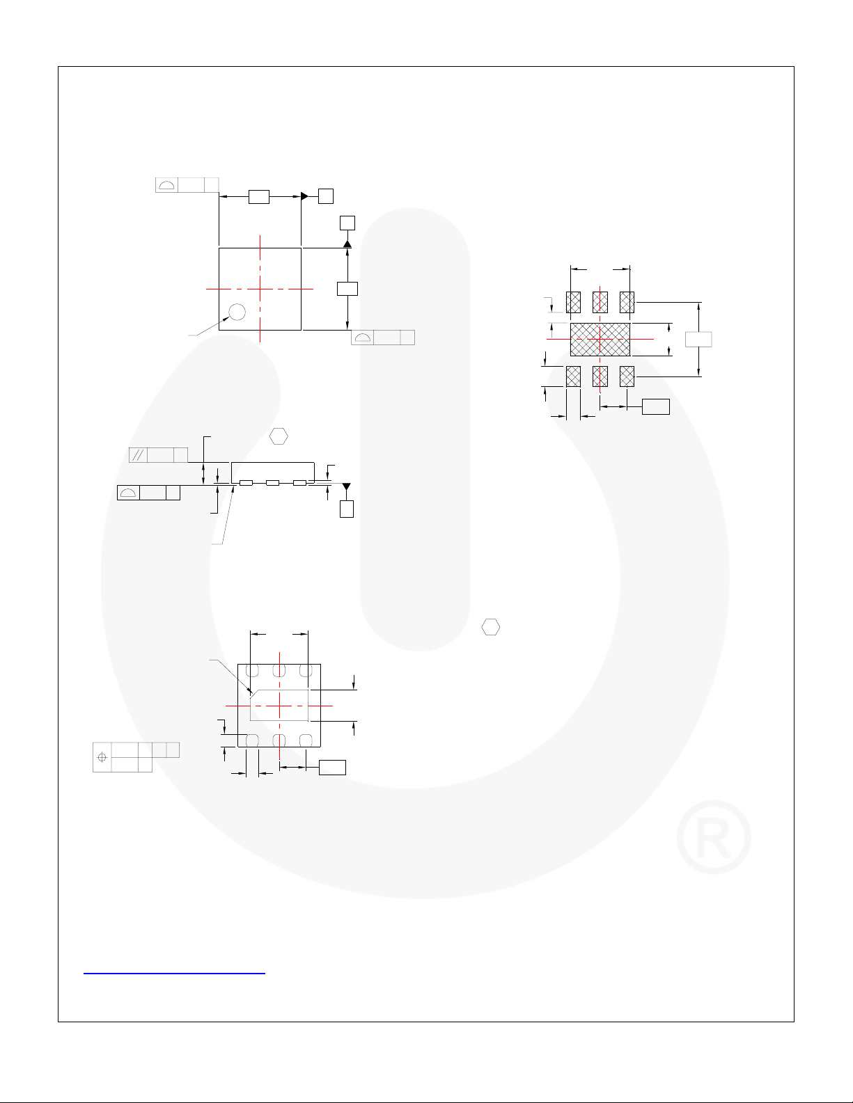
Figure 45. 6-Lead UMLP Package
Package drawings are provided as a service to customers considering Fairchild components. Draw i ngs may change i n any manner wit hout
notice. Please note the revision and/or date on the drawing and contact a Fairchild Semiconductor representative to verify or obtain the most
recent revision. Package specifications do not expand the terms of Fairchild’s worldwide terms and conditions, specifically the warranty therein, which
covers Fairchild products.
Always visit Fairchild Semiconductor’s online packaging area for the most recent package drawings:
http://www.fairchildsemi.com/packaging/
.
© 2010 Fairchild Semiconductor Corporation www.fairchildsemi.com
FAN4860 • Rev. 1.
1.0 16
Page 17
FAN4860 — 3MHz, Synchronous TinyBoost™ Regulator
© 2010 Fairchild Semiconductor Corporation www.fairchildsemi.com
FAN4860 • Rev. 1.
1.0 17
 Loading...