

Page 1
www.fairchildsemi.com
FAN4822
ZVS Average Current PFC Controller
Features
• Average current sensing, continuous boost, leading edge
PFC for low total harmonic distortion and near unity
power factor
• Built-in ZVS switch control with fast response for high
efficiency at high power levels
• A verage line v oltage compensation with bro wnout control
• Current fed gain modulator improves noise immunity and
provides universal input operation
• Overvoltage comparator eliminates output “runaway” due
to load removal
• UVLO, current limit, and soft-start
• Precision 1.3% reference
Block Diagram
1
14
13
4
5
3
6
FB
2.5V
I
AC
V
RMS
I
SENSE
R
TCT
REF
VEAO
VEA
–
+
GAIN
MODULATOR
R+
R–
V
REF
CCZ
8
GND
+
–
IEA
2
IEAO
+
–
OSC
General Description
The FAN4822 is a PFC controller designed specifically for
high power applications. The controller contains all of the
functions necessary to implement an average current boost
PFC converter, along with a Zero Voltage Switch (ZVS) controller to reduce diode recovery and MOSFET turn-on
losses.
The average current boost PFC circuit provides high power
factor (>98%) and low Total Harmonic Distortion (THD).
Built-in safety features include undervoltage lockout, overvoltage protection, peak current limiting, and input voltage
brownout protection.
The ZVS control section drives an external ZVS MOSFET
which, combined with a diode and inductor, soft switches the
boost regulator. This technique reduces diode reverse recovery and MOSFET switching losses to reduce EMI and maximize efficiency.
V
CC
12
PFC OUT
11
ZVS OUT
10
FB
2.7V
–1V
+
–
I LIMIT
+
–
OVP
SRQ
SRQ
V
CCZ
13.5V
Q
ZV SENSE
7
+
––
QS
R
Q
PWR GND
9
REV. 1.0.1 8/10/01
Page 2
FAN4822 PRODUCT SPECIFICATION
Pin Configuration
FAN4822
16-Pin SOIC (S16W)
1
2
3
4
5
6
7
8
TOP VIEW
14-Pin DIP (P14)
VEAO
IEAO
I
SENSE
I
AC
V
RMS
RTC
ZV SENSE
T
Pin Description
FAN4822
1
2
3
4
5
6
7
TOP VIEW
14
13
12
11
10
9
8
FB
REF
V
CC
PFC OUT
ZVS OUT
PWR GND
GND
VEAO
IEAO
I
SENSE
I
V
RMS
RTC
ZV SENSE
N/C
AC
T
(Pin numbers is parentheses are for 16-pin package)
Pin Name Function
1 (1) VEAO Transconductance voltage error amplifier output.
2 (2) IEAO Transconductance current error amplifier output.
3 (3) I
SENSE
4 (4) I
5 (5) V
6 (6) R
AC
RMS
C
T
T
Current sense input to the PFC current limit comparator.
PFC gain modulator reference input.
Input for RMS line voltage compensation.
Connection for oscillator frequency setting components.
7 (7) ZV SENSE Input to the high speed zero voltage crossing comparator.
8 (10) GND Analog signal ground.
9 (11) PWR GND Return for the PFC and ZVS driver outputs.
10 (12) ZVS OUT ZVS MOSFET driver output.
11 (13) PFC OUT PFC MOSFET driver output.
12 (14) V
CC
Shunt-regulated supply voltage.
13 (15) REF Buffered output for the internal 7.5V reference.
14 (16) FB Transconductance voltage error amplifier input.
16
15
14
13
12
11
10
9
FB
REF
V
CC
PFC OUT
ZVS OUT
PWR GND
GND
N/C
Absolute Maximum Ratings
Absolute maximum ratings are those values beyond which the device could be permanently damaged. Absolute maximum ratings are stress ratings only and functional device operation is not implied.
Parameter Min Max Unit
Shunt Regulator Current (I
Peak Driver Output Current ±500 mA
Analog Inputs –0.3 7 V
Junction Temperature 150 °C
Storage Temperature Range –65 150 °C
Lead Temperature (Soldering, 10 sec) 150 °C
Thermal Resistance ( θ
Plastic DIP
Plastic SOIC
2
)55mA
CC
)
JA
80
110
°C/W
°C/W
REV. 1.0.1 8/10/01
Page 3

∆
∆
∆
∆
Ω
PRODUCT SPECIFICATION FAN4822
Operating Conditions
Temperature Range Min. Max. Units
FAN4822IX –40 85 °C
Electrical Characteristics
Unless otherwise specified, R
Parameter Conditions Min. Typ. Max. Units
Voltage Error Amplifier
Input Voltage Range 0 7 V
Transconductance V
Feedback Reference Voltage V
Open Loop Gain 60 75 dB
PSRR V
Output Low 0.65 1 V
Output High 6.0 6.7 V
Source Current
Sink Current
Current Error Amplifier
Input Voltage Range –1.5 2 V
Transconductance V
Input Offset Voltage ±3 ±15 mV
Open Loop Gain 60 75 dB
PSRR V
Output Low 0.65 1 V
Output High 6.0 6.7 V
Source Current
Sink Current
OVP Comparator
Threshold Voltage 2.6 2.7 2.8 V
Hysteresis 80 120 150 mV
I
SENSE
Comparator
Threshold Voltage –0.8 –1.0 –1.15 V
Delay to Output 150 300 ns
ZV Sense Comparator
Propagation Delay 100mV Overdrive 50 ns
Threshold Voltage 7.35 7.5 7.65 V
Input Capacitance 6 pF
= 52.3k Ω , C
T
NON-INV
EAO
CCZ
V
IN
V
IN
NON-INV
CCZ
V
IN
V
IN
= 470pF, T
T
= V
INV
= V
FB
– 3V < V
= ±0.5V, V
= ±0.5V, V
= V
INV
– 3V < V
= ±0.5V, V
= ±0.5V, V
= Operating Temperature Range (Note 1)
A
, VEAO = 3.75V 50 70 120
2.4 2.5 2.6 V
CC
OUT
OUT
< V
– 0.5V 60 75 dB
CCZ
= 6V –40 –80 µA
= 1.5V 40 80 mA
, IEAO = 3.75V 130 195 310
CC
OUT
OUT
< V
– 0.5V 60 75 dB
CCZ
= 6V –30 –80 µ A
= 1.5V 40 80 µ A
µ
µ
Ω
REV. 1.0.1 8/10/01
3
Page 4

FAN4822 PRODUCT SPECIFICATION
Electrical Characteristics (Continued)
Unless otherwise specified, RT = 52.3kΩ, CT = 470pF, TA = Operating Temperature Range (Note 1)
Parameter Conditions Min. Typ. Max. Units
Gain Modulator
Gain (Note 2) I
Bandwidth I
Output Voltage V
Oscillator
Initial Accuracy T
Voltage Stability V
Temperature Stability 2 %
Total Variation Line, temperature 72 89 kHz
Ramp Valley to Peak Voltage 2.5 V
Dead Time 100 300 450 ns
C
Discharge Current 4.5 7.5 9.5 mA
T
Reference
Output Voltage T
Line Regulation V
Load Regulation 1mA < I
Temperature Stability 0.4 %
Total Variation Line, load, and temperature 7.35 7.65 V
Long Term Stability T
Short Circuit Current V
PFC Comparator
Minimum Duty Cycle V
Maximum Duty Cycle V
MOSFET Driver Outputs
Output Low Voltage I
Output High Voltage I
Output Rise/Fall Time C
Undervoltage Lockout
Threshold Voltage V
Hysteresis 2.4 2.9 3.45 V
= 100mA, V
IAC
V
= 0V
FB
I
= 50mA, V
IAC
V
= 0V
FB
I
= 100 µ A, V
IAC
V
= 0V
FB
I
= 100 µ A, V
IAC
V
= 0V
FB
= 250 µ A 10 MHz
IAC
= 0V, V
FB
VRMS
VRMS
VRMS
VRMS
VRMS
= 1.15V, I
= 0V,
= 1.2V,
= 1.8V,
= 3.3V,
IAC
=
0.36 0.51 0.66
1.20 1.72 2.24
0.55 0.78 1.01
0.14 0.20 0.26
0.72 0.8 0.9 V
250 µ A
= 25°C 74 80 87 kHz
A
– 3V < V
CCZ
= 25°C, I
A
– 3V < V
CCZ
REF
= 125°C, 1000 hours 5 25 mV
j
< V
CC
CCZ
> 6.7V 0 %
IEAO
< 1.2V 90 95 %
IEAO
= –20mA 0.4 1.0 V
OUT
I
= –100mA 1.5 3.5 V
OUT
I
= –10mA, V
OUT
= 20mA 9.5 10.3 V
OUT
I
= 100mA 9 10.3 V
OUT
= 1000pF 40 ns
L
< V
CC
= 1mA 7.4 7.5 7.6 V
REF
< V
CC
– 0.5V 1 %
CCZ
– 0.5V 2 10 mV
CCZ
, < 20mA 2 15 mV
– 0.5V, V
CC
= 0V –15 –40 –100 mA
REF
= 8V 0.8 1.5 V
–
V
–
V
CCZ
0.9
CCZ
0.6
CCZ
0.2
–
V
4
REV. 1.0.1 8/10/01
Page 5

PRODUCT SPECIFICATION FAN4822
Electrical Characteristics (Continued)
Unless otherwise specified, RT = 52.3kΩ, CT = 470pF, TA = Operating Temperature Range (Note 1)
Parameter Conditions Min. Typ. Max. Units
Supply
Shunt Voltage (V
)I
CCZ
Load Regulation 25mA < ICC < 55mA ±150 ±300 mV
Total Variation Load and temperature 12.4 14.6 V
Start-up Current VCC < 12.3V 0.7 1.1 mA
Operating Current VCC = V
Notes
1. Limits are guaranteed by 100% testing, sampling, or correlation with worst-case test conditions.
2. Gain = K x 5.3 V; K = (I
GAINMOD
=25mA 12.8 13.5 14.2 V
CC
– 0.5V 22 28 mA
CCZ
– I
OFFSET
) x IAC x (V
EAO
– 1.5)–1.
REV. 1.0.1 8/10/01 5
Page 6
FAN4822 PRODUCT SPECIFICATION
Functional Description
Switching losses of wide input voltage range PFC boost converters increase dramatically as power levels increase above
200 watts. The use of zero-voltage switching (ZVS) techniques improves the efficiency of high power PFCs by significantly reducing the turn-on losses of the boost MOSFET .
ZVS is accomplished by using a second, smaller MOSFET,
together with a storage element (inductor) to convert the
turn-on losses of the boost MOSFET into useful output
power.
The basic function of the FAN4822 is to provide a power
factor corrected, regulated DC bus voltage using continuous,
average current-mode control. Like Micro Linear’s family of
PFC/PWM controllers, the FAN4822 employs leading-edge
pulse width modulation to reduce system noise and permit
frequency synchronization to a trailing edge PWM stage for
the highest possible DC bus voltage bandwidth. For minimization of switching losses, circuitry has been incorporated to
control the switching of the ZVS FET.
Theory of Operation
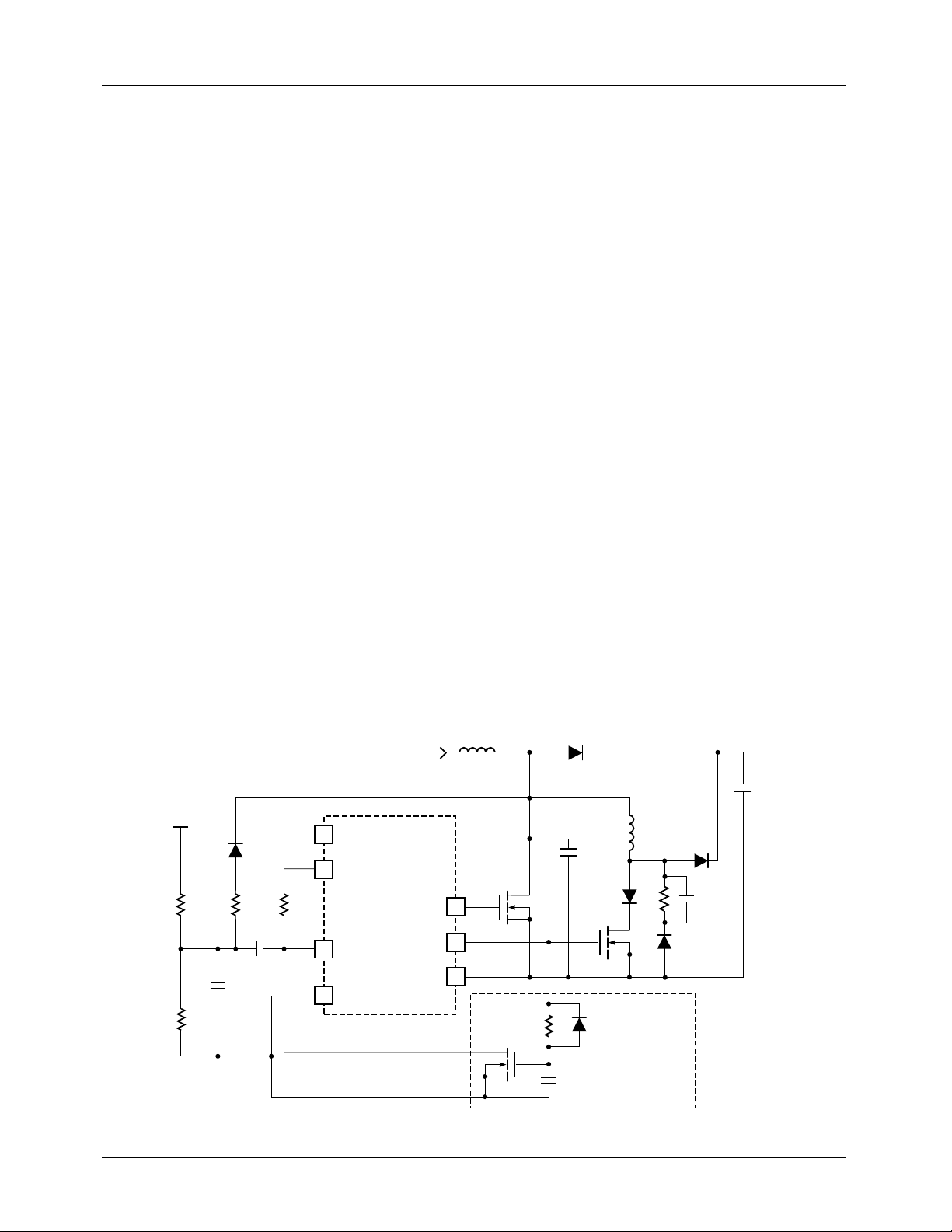
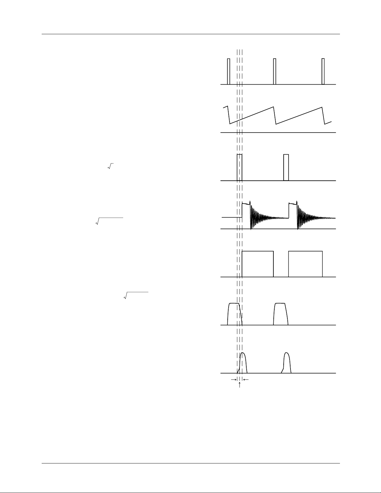
Figure 1 shows a simplified schematic of the output and control sections of a high power PFC circuit. Figure 2 shows the
relationship of various waveforms in the circuit. Q1 functions as the main switching FET and Q2 provides the ZVS
action. During each cycle, Q2 turns on before Q1, diverting
the current in L1 away from D1 into L2. The current in L2
increases linearly until at t2 it equals the current through L1.
When these currents are equal, L1 ceases discharging current
and is now charged through L2 and Q2. At time t2, the drain
voltage of Q1 begins to fall. The shape of the voltage waveform is sinusoidal due to the interaction of L2 and the com-
bined parasitic capacitance of D1 and Q1 (or optional ZVS
capacitor C
). At t3, the voltage across Q1 is sufficiently
ZVS
low that the controller turns Q2 off and Q1 on. Q1 then
behaves as an ordinary PFC switch, storing energy in the
boost inductor L1. The energy stored in L2 is completely discharged into the boost capacitor via D2 during the Q1 offtime and the value of L2 must be selected for discontinuousmode operation.
Component Selection
Q1 Turn-Off
Because the FAN4822 uses leading edge modulation, the
PFC MOSFET (Q1) is always turned off at the end of each
oscillator ramp cycle. For proper operation, the internal ZVS
flip-flop must be reset every cycle during the oscillator discharge time. This is done by automatically resetting the ZVS
comparator a short time after the drain voltage of the main Q
has reached zero (refer to Figure 1 sense circuit). This sense
circuit terminates the ZVS on time by sensing the main Q
drain voltage reaching zero. It is then reset by way of a resistor pull-up to VCC (R6). The advantage of this circuit is that
the ZVS comparator is not reset at the main Q turn off which
occurs at the end of the clock cycle. This av oids the potential
for improper reset of the internal ZVS flip-flop.
Another concern is the proper operation of the ZVS comparator during discontinuous mode operation (DCM), which
will occur at the cusps of the rectified AC waveform and at
light loads. Due to the nature of the voltage seen at the drain
of the main boost Q during DCM operation, the ZVS comparator can be fooled into forcing the ZVS Q on for the
entire period. By adding a circuit which limits the maximum
on time of the ZVS Q, this problem can be avoided. Q3 in
Figure 1 provides this function.
L1
V
REF
R3
22k
R4
51k
C4
330pF
R5
220
33pF
C3
R6
22k
13
12
7
8
V
REF
FAN4822
V
C
C
ZV SENSE
GND
PFC OUT
ZVS OUT
PWR GND
Q1
11
10
9
Q3
R2
D1
C
C5
ZVS(OPT)
Q2
MAX ZVS
ON TIME LIMIT
+
C1
L2
D2
R1
C2
Figure 1. Simplified PFC/ZVS Schematic.
6 REV. 1.0.1 8/10/01
Page 7
PRODUCT SPECIFICATION FAN4822
Q1 Turn-On
The turn-on event consists of the time it takes for the current
through L2 to ramp to the L1 current plus the resonant event
of L2 and the ZVS capacitor. The total event should occur in
a minimum of 350–450ns, but can be longer at the risk of
A. SYSTEM
CLOCK
(INTERNAL)
increasing the total harmonic distortion. Setting these times
equal should minimize conducted and radiated emissions.
= t
t
Q1 OFF()tIL2
+ 400ns=
RES
(1)
B. R
TCT
Where I
is equal to IL1.
L2
The value of L2 is calculated to remain in discontinuousmode:
V
BUSVRMS MIN()tIL2
L2
---------------------------------------------------------------- -=
2P
×
OUT
××
(2)
The resonant event occurs in 1/4 of a full sinusoidal cycle.
For example, when a 1/4 cycle occurs in 200ns, the frequency is 1.25MHz.
f
RES
1
-----------------------------------
2π
L2 C
×
ZVS
1
---------------------==
×
4t
RES
(3)
Rearranging and solving for L2:
4t
×
2
RES
--------------------------=
L2
2
π
C
×
ZVS
The resonant capacitor (C
) value is found by setting
ZVS
equations 2 and 4 equal to each other and solving for C
4t
C
ZVS
× 2P
RES
-----------------------------------------------------------------------------=
2
π
V
BUSVRMS MIN()tIL2
××
2
OUT
×××
(4)
ZVS
(5)
C. ZVS GATE (Q2)
D. VDS (Q2)
E. PFC GATE (Q1)
.
F. VDS (Q1)
Application
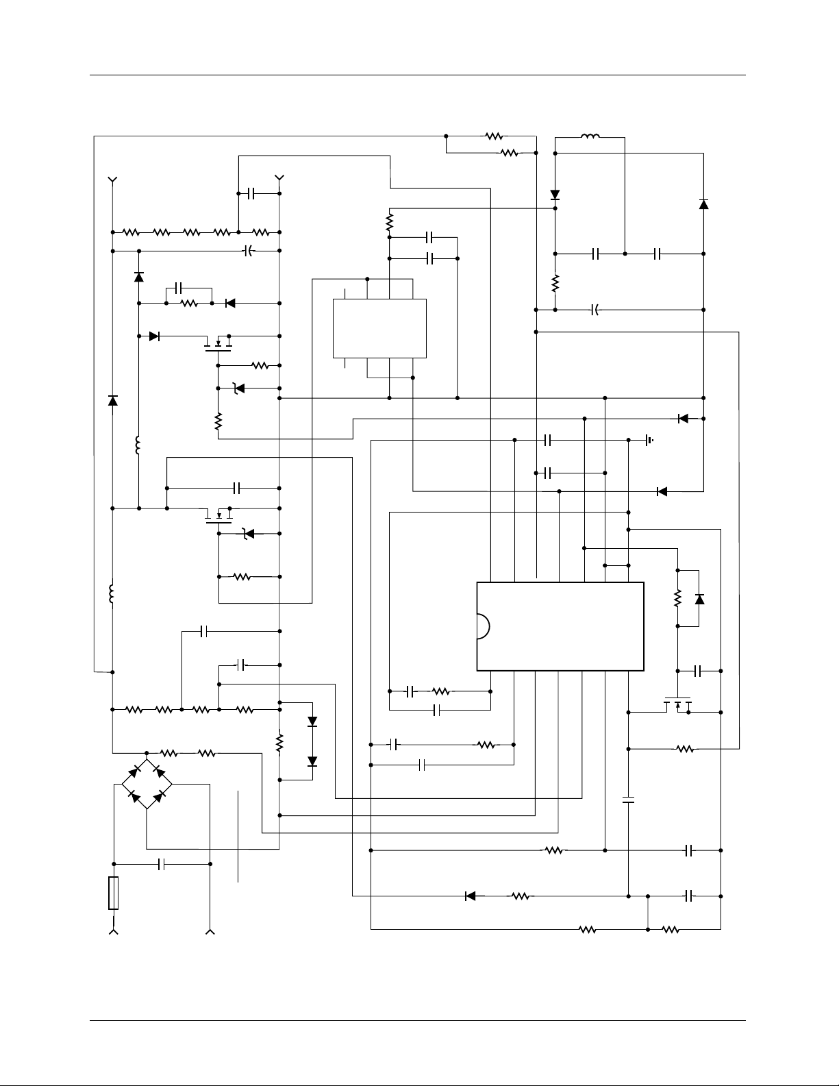
Figure 3 displays a typical application circuit for a 500W
ZVS PFC supply. Full design details are covered in application note 33, FAN4822 Power Factor Correction With Zero
Voltage Resonant Switching.
REV. 1.0.1 8/10/01 7
G. I
L2
t
1
t
3
t
2
Figure 2. Timing Diagrams
Page 8
FAN4822 PRODUCT SPECIFICATION
L1
R5
39kΩ
2W
n = 2.5
400VDC
D1
R10
102kΩ 1%
D2
MUR860
D3
FESI6JT
L2
L1
420uH @ 10A
n = 57
R12
453kΩ 1%
B1
R9
R8
93.1kΩ 1%
C21
0.1µF
R1
3.3kΩ
Q2
MUR460
8.5m @ 14A
Q1
R22
453kΩ 1%
R13
402kΩ
1%
R20
93.1kΩ 1%
93.1kΩ 1%
200V
D4
3W
FQP6N50
R3
10
FQA24N50
C4
0.1µF
R14
100kΩ 1%
R23
402kΩ
1%
C3
R11
+
C1
UF4005
D6
1N4747A
C2
R4
10kΩ
50V
C6
R15
16.2kΩ
1000pF
50V
2.37kΩ
1%
450V
330µF
R6
10kΩ
470pF
1600V
D5
1N4747A
16V
0.47µF
1%
400VDC RTN
R18
0.0732 5W 1%
TC4427
D7
1N5401
D13
1N5401
2W
R21
39kΩ
D11
EGP20A
R2
10Ω
8
7
6
S
OUT A
IN A
2
3
V
S RTN
V
C12
NC
NC
1
5
OUT B
IN B
4
C7
2.2nF
C10
0.68µF 50V
50V
C9
C13
1µF
1µF
R17
100pF
50V
50V
220kΩ
C11
50V
68nF
14
FB
FAN4822
VEAO
1
50V
R19
10kΩ
13
2
REF
IEAO
12
CC
V
SENSEIAC
I
3
R7
C5
1µF
C8
2.2µF
11
PFC OUT
4
47
50V
50V
10
ZVS OUT
RMS
V
5
50V
C16
1µF
25V
C15
1500µF
9
PWR GND
T
C
T
R
6
8
GND
ZV SENSE
7
C18
C17
R29
Q3
33pF
1µF
D9
1N5819
10kΩ
2N7000
50V
50V
R26
D8
1N5819
22kΩ
C22
D12
1N4148
100pF
EGP20A
GBU6G
1%
R16
D10
C14
0.47µF
F1
8AMP
250VAC
LINE
250VAC
NEUTRAL
UF4005
R27
220
8.25kΩ
R24
22kΩ
R25
C20
2.2nF
50V
C19
330pF
50V
51kΩ
Figure 3. FAN4822 Schematic.
8 REV. 1.0.1 8/10/01
Page 9

PRODUCT SPECIFICATION FAN4822
3
Mechanical Dimensions inches (millimeters)
Package: P14
14-Pin PDIP
0.740 - 0.760
(18.79 - 19.31)
14
0.070 MIN
(1.77 MIN)
(4 PLACES)
0.170 MAX
(4.32 MAX)
16
0.125 MIN
(3.18 MIN)
0.400 - 0.414
(10.16 - 10.52)
PIN 1 ID
1
0.050 - 0.065
(1.27 - 1.65)
0.100 BSC
(2.54 BSC)
0.016 - 0.022
(0.40 - 0.56)
0.240 - 0.260
(6.09 - 6.61)
0.015 MIN
(0.38 MIN)
SEATING PLANE
Package: S16W
16-Pin Wide SOIC
0.295 - 0.325
(7.49 - 8.25)
0º - 15º
0.008 - 0.012
(0.20 - 0.31)
0.024 - 0.034
(0.61 - 0.86)
(4 PLACES)
0.090 - 0.094
(2.28 - 2.39)
1
PIN 1 ID
0.050 BSC
(1.27 BSC)
0.012 - 0.020
(0.30 - 0.51)
0.291 - 0.301
(7.39 - 7.65)
0.095 - 0.107
(2.41 - 2.72)
SEATING PLANE
0.398 - 0.412
(10.11 - 10.47)
0.005 - 0.013
(0.13 - 0.33)
0º - 8º
0.022 - 0.042
(0.56 - 1.07)
0.009 - 0.01
(0.22 - 0.33)
REV. 1.0.1 8/10/01 9
Page 10

FAN4822 PRODUCT SPECIFICATION
Ordering Information
Part Number PFC/PWM Frequency Package
FAN4822IN
FAN4822IM
-40°C to 85°C
-40°C to 85°C
14-Pin PDIP (P14)
16-Pin Wide SOIC (S16W)
DISCLAIMER
FAIRCHILD SEMICONDUCTOR RESERVES THE RIGHT TO MAKE CHANGES WITHOUT FURTHER NOTICE TO
ANY PRODUCTS HEREIN TO IMPROVE RELIABILITY, FUNCTION OR DESIGN. FAIRCHILD DOES NOT ASSUME
ANY LIABILITY ARISING OUT OF THE APPLICATION OR USE OF ANY PRODUCT OR CIRCUIT DESCRIBED HEREIN;
NEITHER DOES IT CONVEY ANY LICENSE UNDER ITS PATENT RIGHTS, NOR THE RIGHTS OF OTHERS.
LIFE SUPPORT POLICY
FAIRCHILD’S PRODUCTS ARE NOT AUTHORIZED FOR USE AS CRITICAL COMPONENTS IN LIFE SUPPORT DEVICES
OR SYSTEMS WITHOUT THE EXPRESS WRITTEN APPROVAL OF THE PRESIDENT OF FAIRCHILD SEMICONDUCTOR
CORPORATION. As used herein:
1. Life support devices or systems are devices or systems
which, (a) are intended for surgical implant into the body,
or (b) support or sustain life, and (c) whose failure to
perform when properly used in accordance with
instructions for use provided in the labeling, can be
reasonably expected to result in a significant injury of the
user.
www.fairchildsemi.com
2. A critical component in any component of a life support
device or system whose failure to perform can be
reasonably expected to cause the failure of the life support
device or system, or to affect its safety or effectiveness.
8/10/01 0.0m 003
2001 Fairchild Semiconductor Corporation
Stock#DS30004803
 Loading...