

Page 1
查询FAN5607供应商查询FAN5607供应商
www.fairchildsemi.com
FAN5607
LED Driver with Adaptive Charge Pump DC/DC
Converter
Features
•Parallel LED Driver Supports all Forward Voltages
• Adaptive V
Adjustment to the Highest Diode Voltage
OUT
• Internally Matched LED Current Sources
• Built-in Charge Pump has Three Modes of Operation:
– 1X, 1.5X, and 2X Mode
• Up to 93% Efficiency
•Low EMI, Low Ripple
• Up to 120mA Output Current ( )
30mA×
4
• External Resistor to Set Maximum (100%) LED Current
• Enable Input Can be Duty-Cycle-Modulated to Control
LED Current Level Between 0 and 100%
• 2.4V to 5.5V Input Voltage Range
•I
< 1µA in Shutdown Mode
CC
• 1MHz Operating Frequency
• Shutdown Isolates Output from Input
• Soft-Start Limits Inrush Current
• Short Circuit Protection
• Minimal External Components Needed
•Available in a 4x4mm 16-lead MLP Package
Applications
• Cell Phones
• Handheld Computers
•PDA, DSC, MP3 Players
•Keyboard Backlight
• LED Displays
Description
The FAN5607 generates regulated output current from a battery with input voltage varying between 2.7V to 5.5V.
Switch reconfiguration and fractional switching techniques
are utilized to achieve high efficiency over the entire input
voltage range. A proprietary internal circuitry continuously
monitors each LED current loop and automatically adjusts
the generated output DC voltage to the lowest minimum
value required by the LED having the highest forward voltage. This adaptive nature of the FAN5607 eliminates the
need for LED pre-selection (matching) and ensures operation at high efficiency. When the input voltage is sufficiently
high to sustain the programmed current level in the LEDs,
the FAN5607 re-configures itself to operate as a linear regulator, and the DC-DC converter is turned off. Only two 0.1µF
to 1µF bucket capacitors and two 4.7µF input/output capacitors are needed for proper operation. LED current can be
programmed using an external resistor. The resistor sets the
maximum LED current and a PWM signal applied to the
enable pin can modulate that current level between 0mA
(off) and the maximum level.
Soft-start circuitry prevents excessive current draw during
power on. The device has built-in short circuit protection.
The device is available in 4x4mm 16-lead MLP package.
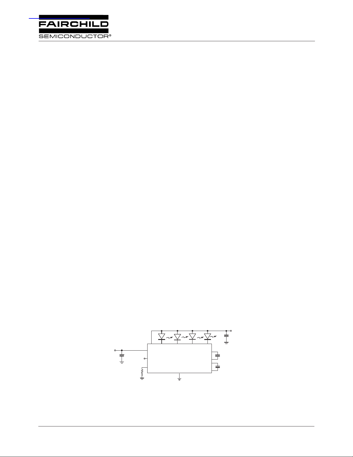
Typical Application
V
OUT
C
OUT
V
IN
C
IN
V
OUT
V
IN
EN
R
SET
R
SET
FAN5607
GND
LED-LED-LED-LED-
CAP-
CAP+
CAP+
CAP-
CAP2
CAP1
REV. 1.0.0 6/22/04
Page 2

FAN5607 PRODUCT SPECIFICATION
Definition of Terms
Output Current Accuracy: reflects the difference between the measured value of the output current (LED) and
programmed value of this current .
I
Output Current Accuracy (%)
=
-------------------------------------------------------------------------------------------------------------------I
OUT
measured I
OUT
Current Matching: refers to the absolute value of difference in current between the two LED branches.
programmed–()100×
OUT
programmed
Current Matching (%)
branch 1 I
I
LED
=
----------------------------------------------------------------------------------------------------I
branch 1 I
LED
branch 2–()100×
LED
branch 2+()
LED
Efficiency: is expressed as a ratio between the electrical power into the LEDs and the total power consumed from the input
power supply.
4
V
∑
i1=
Efficiency
Note:
1. Some competitors calculate the power efficiency as a function of V
due to the cathode and provides an efficiency “improved” up to 5%.
=
--------------------------------------------
×
LEDiILEDi
VINIIN×
voltage 0≠
instead of V
OUT
. This method neglects the power lost
LED
2
REV. 1.0.0 6/22/04
Page 3
PRODUCT SPECIFICATION FAN5607
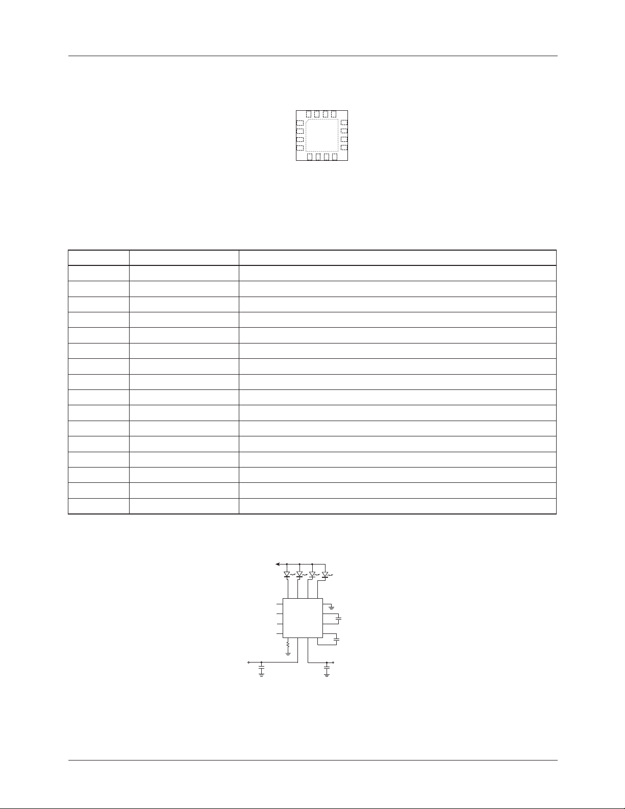
Pin Assignments
Top-View
LED-
LED-
LED-
LED-
1
EN
2
NC
3
NC
4
NC
13141516
12
GND
11
CAP2+
10
CAP2-
9
CAP1-
7
5
6
8
IN
SET
V
OUT
R
V
CAP1+
FAN5607
4x4mm 16-Lead MLP
Pin Descriptions
Pin No. Pin Name Pin Function Description
1ENEnable Pin
2NCNo Connection
3NCNo Connection
4NCNo Connection
5R
6V
7V
SET
OUT
IN
8 CAP1+ Bucket capacitor positive connection
9 CAP1- Bucket capacitor negative terminal
10 CAP2- Bucket capacitor negative connection
11 CAP2+ Bucket capacitor positive terminal
12 GND Ground
13 LED- 4th LED Cathode
14 LED- 3rd LED Cathode
15 LED- 2nd LED Cathode
16 LED- 1st LED Cathode
External resistor to set LED current
Output to LEDs Anode
Input
Test Circuit
REV. 1.0.0 6/22/04
To V
Pin
OUT
16
1
EN
NC
FAN5607
NC
4
NC
5
R
SET
V
= 2.7V to 5.5V
IN
4.7µF
C
IN
All capacitors are Ceramic chip capacitors
Figure 1. Test Circuit
4.7µF
13
12
CAP2
1µF
OUT
OUT
CAP1
1µF
4 White LEDs
Fairchild QTLP670C-IW
Super Bright LED
9
8
V
C
3
Page 4
FAN5607 PRODUCT SPECIFICATION
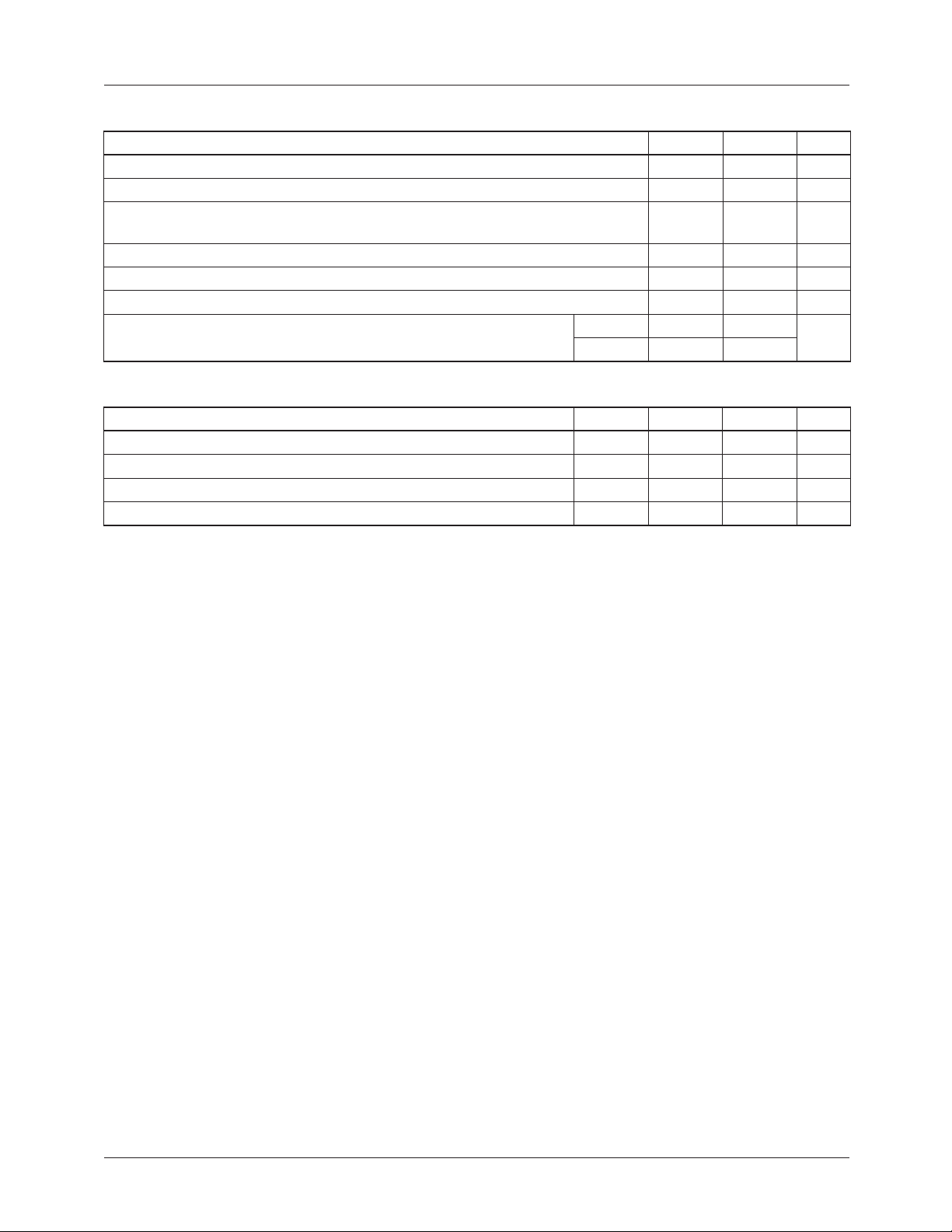
Absolute Maximum Ratings
Parameter Min Max Unit
V
, V
IN
Any other Pin Voltage to GND -0.3 V
Power Dissipation Internally
Lead Soldering Temperature (10 seconds) 300 °C
Operating Junction Temperature Range 150 °C
Storage Temperature -55 150 °C
Electrostatic Discharge Protection Level (Note 3) HBM 4 kV
Voltage to GND -0.3 6.0 V
OUT
(
Note 2)
CDM 2
+ 0.3 V
IN
Limited
Recommended Operating Conditions
Parameter Min Typ Max Unit
Input Voltage Range, V
Operating Ambient Temperature Range -40 25 85 °C
LED Forward Voltage 4V
Current through each LED 2 30 mA
Note:
2. Operation beyond the absolute maximum ratings may cause damage to device.
3. Using Mil Std. 883E, method 3015.7(Human Body Model) and EIA/JESD22C101-A (Charge Device Model)
2.4 5.5 V
IN
4
REV. 1.0.0 6/22/04
Page 5

PRODUCT SPECIFICATION FAN5607
Electrical Characteristics
V
= 2.7V to 5.5V, T
IN
Typical values are at T
Input Undervoltage Lockout 1.7 1.8 2.3 V
I
Accuracy 5%
LED
Current Matching 3 %
Output Voltage (V
Quiescent Current, I
Shutdown Supply Current V
Output Short Circuit Current V
V
Over Voltage Protection 5.1 V
OUT
V
At Mode Transition From 1X to 1.5X LED V
IN
V
At Mode Transition From 1.5X to 2X LED V
IN
Peak Efficiency V
Oscillator Frequency 0.8 1 1.2 MHz
Thermal Shutdown Threshold 145 ºC
Thermal Shutdown Hysteresis 15 ºC
EN Logic Input High Voltage 1.6 V
EN Logic Input Low Voltage 0.4 V
EN Input Bias Current EN to V
= -40ºC to +85ºC, Test Circuit Figure 1, Unless otherwise noted.
A
= 25˚C
A
Parameter Conditions Min. Typ. Max. Units
I
20mA≤
LED
I
20mA≤
LED
= V
OUT
+ V
f
Q
) LED V
Cathode
V
I
OUT
V
I
OUT
I
OUT
IN
LED V
I
LED
IN
IN
OUT
= 3.5V 3.62 V
f
= 5.5V,
130 400 µA
= 0mA
= 0V 1 µA
EN
= 5.5V,
65 mA
= 0V
= 3.5V,
f
3.76 V
= 4 x 20mA
= 3.5V,
f
2.85 V
= 4 x 20mA
= 3.75V,
= 3.5V,
f
93 %
= 20mA
or GND -1 1 µA
IN
REV. 1.0.0 6/22/04
5
Page 6
FAN5607 PRODUCT SPECIFICATION
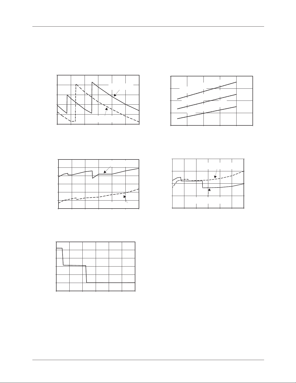
Typical Performance Characteristics
T
= 25°C, C
A
otherwise noted.
= C
IN
=4.7 µ F, CAP1 = CAP1 = 0.1 µ F, FAN5607 driving four LEDs with V
OUT
= 3.5V at 20mA, unless
f
Efficiency vs Battery Voltage
1.0
0.9
0.8
0.7
I
LED
= 20mA
Efficiency
0.6
0.5
2.5 3.0 3.5 4.0 4.5 5.0 5.5
I
LED
=2mA
Battery Voltage (V)
LED Cathode Voltage vs Battery Voltage
0.14
0.13
0.12
0.11
0.10
0.09
LED Cathode Voltage (V)
0.08
2.5 3.0 3.5 4.0 4.5 5.0 5.5
Battery Voltage (V)
I
LED
= 20mA
I
LED
=2mA
Upper Mode Change Voltage vs
4.5
4.0
3.5
3.0
Battery Voltage (V)
2.5
051015 20 25
LED Forward Voltage
m
0
2
=
D
I
E
L
t
a
V
4
=
V
F
a
V
5
.
3
=
V
F
V
3
=
V
F
LED Cur rent ( mA)
2
=
D
I
E
L
t
2
=
D
E
I
L
t
a
A
A
m
0
A
m
0
LED Current vs BatteryVoltage
22
I
=2mA
LED
21
20
19
High LED Current (mA)
18
2.5 3.0 3.5 4.0 4.5 5.0 5.5
I
=20mA
LED
Battery Voltage (V)
2.2
2.1
2.0
1.9
Low LED Current (mA)
1.8
Supply Current vs Battery Voltage
180
160
140
120
100
Supply Current (mA)
80
60
2.5 3.0 3.54.04.55.0 5.5
Battery Voltage ( V)
6
REV. 1.0.0 6/22/04
Page 7
PRODUCT SPECIFICATION FAN5607
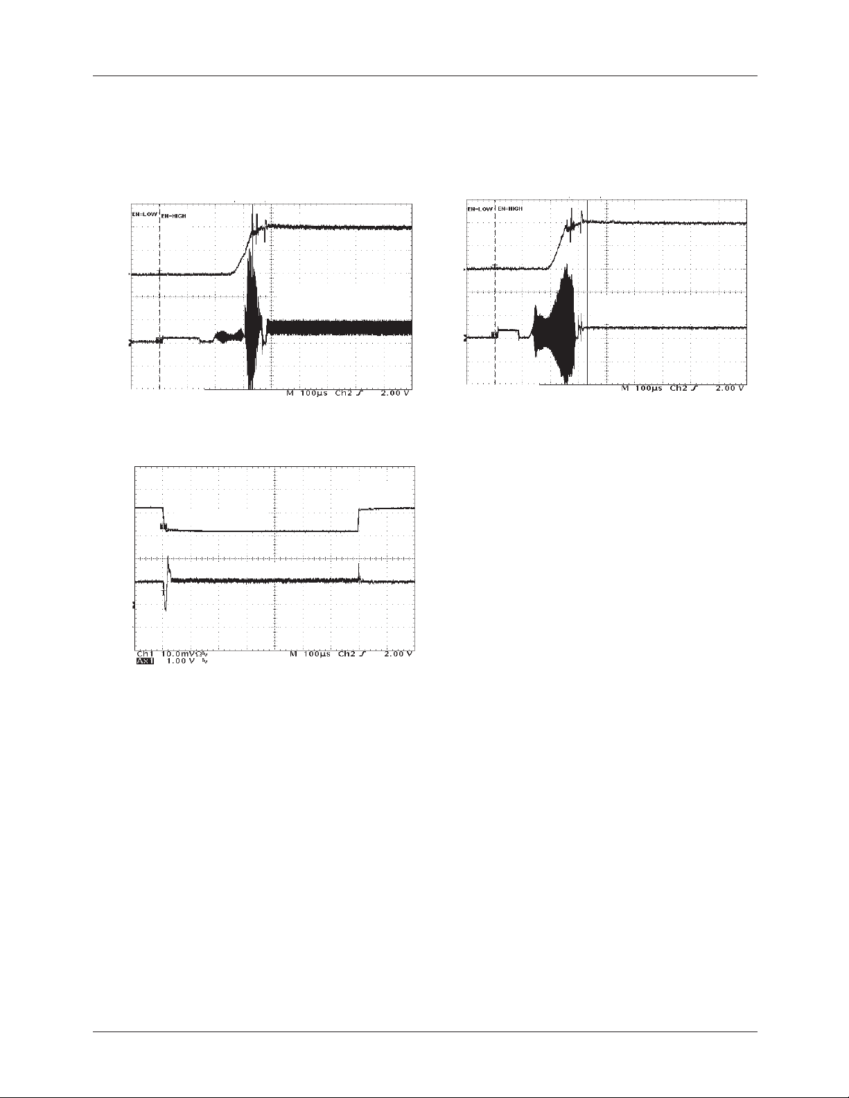
Typical Performance Characteristics
T
= 25°C, C
A
otherwise noted.
(10mA/div)
LED Current
(200mA/div)
Input Current
IN
= C
= 4.7 µ F, CAP1 = CAP1 = 0.1 µ F, F AN5607 driving four LEDs with V
OUT
Startup at VIN=3.6V
Time (100µs/div)
Line Transient Response
I
= 20mA
LED
Input current when driving
4LEDsx20mA
VIN=4.2V
(cont.)
= 3.5V at 20mA, unless
f
Startup at VIN=5V
I
= 20mA
LED
(10mA/div)
LED Current
Input current when driving
4LEDsx20mA
(200mA/div)
Input Current
Time (100µs/div)
(1V/div)
Input Voltage
(10mA/div)
LED Current
VIN=3.2V
Time (100µs/div)
REV. 1.0.0 6/22/04
7
Page 8
FAN5607 PRODUCT SPECIFICATION
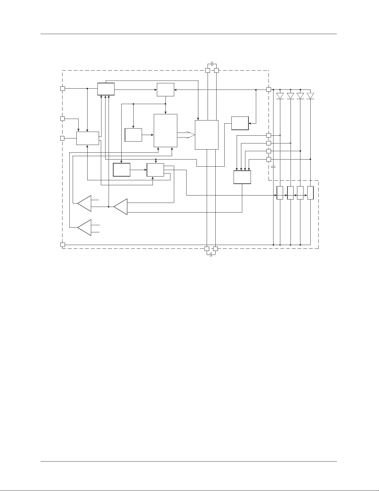
Block Diagram
1µF
V
OUT
V
IN
Linear
Regulator
Voltage
Selector
EN
R
SET
GND
On Off
And
Current Range
Mode Change
Ref1
V
IN
Ref4 (BG)
Oscillator
Bandgap
Reference
Range Selection
Low Battery Ref.
Regulator
D
R
I
V
E
R
S
Reference
Ref3
Figure 2. Block Diagram
Power
Ref2
Good
Analog
Detector
5µF
I. LIM.
I. LIM.
I. LIM.
I. LIM.
P
U
M
P
1µF
Circuit Description
The FAN5607’s switched capacitor DC/DC converter automatically configures its internal switches to achieve high
efficiency and to provide tightly regulated output currents for
the LEDs. An analog detector determines which diode
requires the highest voltage in order to sustain the pre-set
current levels, and adjusts the pump regulator accordingly.
Every diode has its own linear current regulator. In addition,
a voltage regulator controls the output voltage when the battery voltage is within a range where linear regulation can
provide maximum possible efficiency. If the battery voltage
is too low to sustain the diode current in the linear mode, a
fractional 3:2 charge pump is enabled. When the battery
voltage drops further and this mode is no longer sufficient to
sustain proper operation, the pump is automatically reconfig-
the voltage decays, the FAN5607 switches between modes to
maintain a constant current through LED throughout the battery life. The transition has hysteresis to prevent toggling.
Supply Voltage
The internal supply voltage for the device is automatically
selected from VIN or V
Soft Start
The soft-start circuit limits inrush current when the device is
initially powered up and enabled. The reference voltage controls the rate of the output voltage ramp-up to its final value.
Typical start-up time is 0.4ms. The rate of the output voltage
ramp-up is controlled by an internally generated slow ramp,
and an internal variable resistor limits the input current.
pins, whichever is higher.
OUT
ured to operate in 2:1 mode. As the battery discharges and
8 REV. 1.0.0 6/22/04
Page 9
PRODUCT SPECIFICATION FAN5607
Switch Configurations
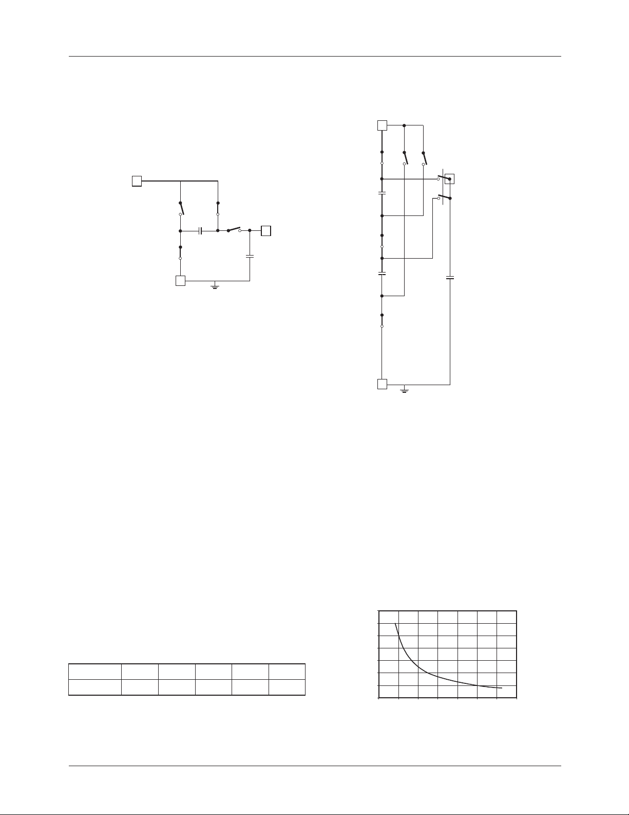
V
IN
V
IN
GND
Figure 3. Step-up, 2:1 Configuration
Switch positions shown in charge phase
Reverse all switches for pump phase
V
OUT
= 2 X V
+
CAP1
-
IN
+
CAP2
-
V
OUT
C
OUT
Shutdown and Short Circuit Current Limit
Set both DAC inputs low to shut down the device. Built-in
short circuit protection limits the supply current to a maximum of 65mA.
LED Brightness Control Methods
R
Only-Analog
SET
The basic method is to use external resistor to set the LED
current. Connect the resistor with the appropriate value
between R
R
SET
(mA) 30 20 10 5 4
I
LED
and GND to set the LED current.
SET
(KΩ) 8.25 12.5 25 50 62.5
GND
Figure 4. Step-up, 3:2 Configuration
Switch positions shown in charge phase
Reverse all switches for pump phase
The resistor value establishes the reference current needed
for a constant LED current. Value of R
for a fixed LED
SET
current are given in the table above and also in the graph
below, using the function: R
LED Current vs R
35
30
25
20
15
10
5
LED Current (mA)
0
010203040506070
SET
R
= 250/I
(KΩ)
SET
LED
SET
.
REV. 1.0.0 6/22/04 9
Page 10
FAN5607 PRODUCT SPECIFICATION
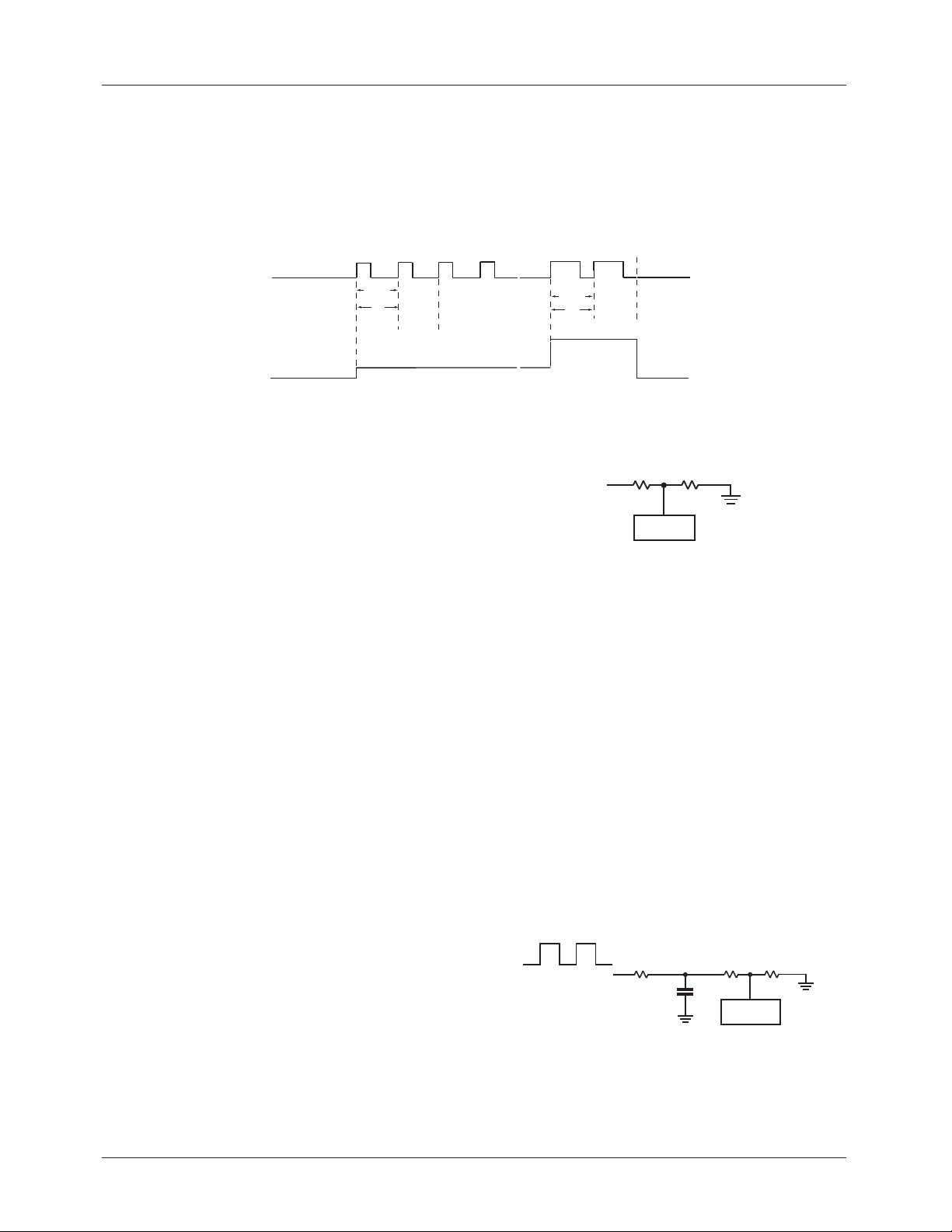
PWM Control
Unless otherwise noted, R
Enable is Controlled by PWM Signal
= 12.5KΩ, I
SET
LED_MAX
= 20mA
ENABLE Input (PWM)
30%
Duty Cycle
1KHz
I
LED
0mA
I
PWM Control
Once R
(I
LED_MAX
is chosen to set maximum LED current
SET
), PWM modes can be used for brightness control. By turning the ENABLE pin ON and OFF, the current
can be modulated between 0 to I
I
value. In PWM mode, the modulating frequency has
Average
LED_MAX
to achieve any
to be set sufficiently high in order to avoid a flickering effect
(50Hz to 100Hz).
The best LED to LED matching and the purest white light
are achieved over the entire range of average current settings,
when the PWM brightness control is used to modulate the
LED current between zero and the maximum value.
Application Information
Brightness Control
LED
(Average)
s
s
70%
Duty Cycle
1KHz
I
(Average)
= 0.3 x I
LED-MAX
V
= 0.7 x I
EXT
LED
s
s
LED-MAX
OFF
R2
I
SET
FAN5607
R1
Figure 5. DC Voltage Control
The FAN5607 internal circuit maintains a constant I
age = 0.5V. Adjusting V
changes the I
EXT
accordingly.
Selecting different values for R1, R2 and V
I
variation range can be changed according to the rela-
LED
tion:
I
LED
250
---------R1
250 500 V
---------------------------------------------------+=
×–()
EXT
R2
mA
SET
range, the
EXT
SET
and I
volt-
LED
1. Dimming Using PWM at EN Pin
A PWM signal applied to EN can control the LED brightness
in direct dependence on the duty cycle. The recommended
PWM signal frequency is 100Hz to ensure a good match
between the input signal duty cycle and the LED average
current. If this ripple frequency is too low for a particular
noise sensitive application, then DC-based dimming control
circuits or higher-frequency-filtered PWM signals may be
Where 0V < V
3. Dimming Using a Filtered PWM Signal
The external PWM signal is filtered by an R3C network
resulting in a DC component dependent on the PWM signal
duty cycle as shown in Figure 6. The resistor R3 needs to be
much smaller than R2 and the corner frequency of R3C
group is much smaller than the PWM signal frequency.
< 0.5V and R1 and R2 are in KΩ.
EXT
used.
2. Dimming with DC Voltage
The brightness control using a variable DC voltage is shown
in Figure 5. If R1=125kΩ, R2=13.9kΩ, adjusting V
EXT
in the
(0V to 0.5V) range results in dimming the LED current from
20mA to 2mA.
C
Figure 6. Filtered PWM Control
R2R3 R1
I
SET
FAN5607
10 REV. 1.0.0 6/22/04
Page 11
PRODUCT SPECIFICATION FAN5607
Selecting Capacitors
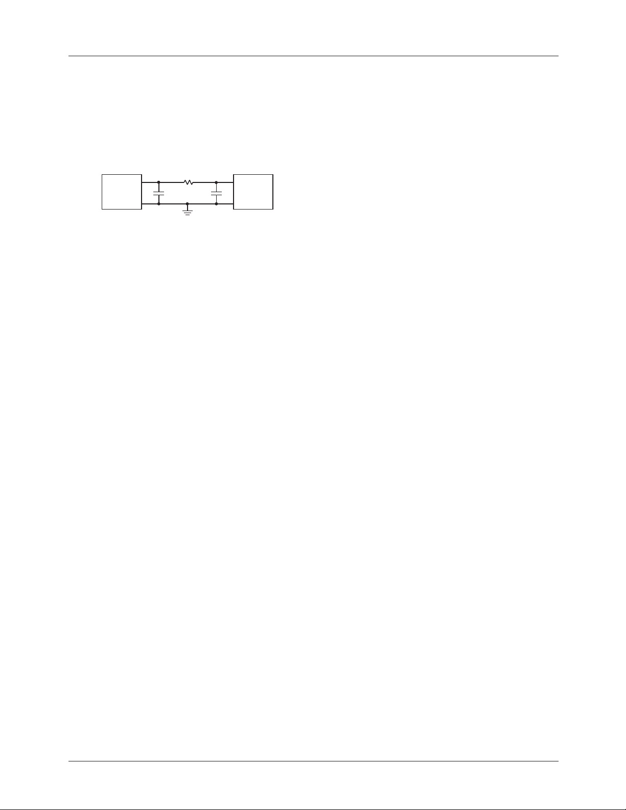
It is important to select the appropriate capacitor types and
the values for use with the FAN5607. These capacitors determine parameters such as power efficiency, maximum sustainable load current by the charge pump, input and output
ripple and start-up process.
Input
Powe r
Supply
Figure 7. Battery Ripple Reduction
In order to reduce ripple, both C
ESR capacitors. Increasing the C
10µF
0.22Ω
4.7µF
and C
IN
OUT
output ripple voltage. However this will increase the poweron time. The CIN value controls input ripple. If necessary,
this ripple can be further reduced by powering the FAN5607
V
IN
FAN5607
GND
should be low
OUT
capacitor reduces the
through the RC input filter, as shown in Figure 7. Two low
ESR bucket capacitors of value between 0.1µF to 1µF,
should be used for best efficiency in boost mode. The bucket
capacitor, CAP1 = CAP2 = 1µF is recommended, if the
FAN5607 is required to start at battery voltage lower than
3V.
PC Board Layout
For best performance, a solid ground plane is recommended
on the back side of the PCB. The ground tails of C
C
should be connected together close to the GND pin of
OUT
IC.
IN
and
REV. 1.0.0 6/22/04 11
Page 12
FAN5607 PRODUCT SPECIFICATION
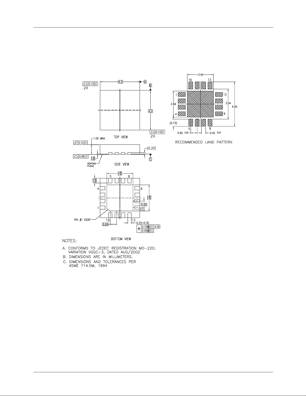
Mechanical Dimensions
4x4mm 16-Lead MLP Package
12 REV. 1.0.0 6/22/04
Page 13

FAN5607 PRODUCT SPECIFICATION
Ordering Information
Product Number Package Type Order Code
FAN5607 4x4mm 16-Lead MLP FAN5607HMPX
DISCLAIMER
FAIRCHILD SEMICONDUCTOR RESERVES THE RIGHT TO MAKE CHANGES WITHOUT FURTHER NOTICE TO
ANY PRODUCTS HEREIN TO IMPROVE RELIABILITY, FUNCTION OR DESIGN. FAIRCHILD DOES NOT ASSUME
ANY LIABILITY ARISING OUT OF THE APPLICATION OR USE OF ANY PRODUCT OR CIRCUIT DESCRIBED HEREIN;
NEITHER DOES IT CONVEY ANY LICENSE UNDER ITS PATENT RIGHTS, NOR THE RIGHTS OF OTHERS.
LIFE SUPPORT POLICY
FAIRCHILD’S PRODUCTS ARE NOT AUTHORIZED FOR USE AS CRITICAL COMPONENTS IN LIFE SUPPORT DEVICES
OR SYSTEMS WITHOUT THE EXPRESS WRITTEN APPROVAL OF THE PRESIDENT OF FAIRCHILD SEMICONDUCTOR
CORPORATION. As used herein:
1. Life support devices or systems are devices or systems
which, (a) are intended for surgical implant into the body,
or (b) support or sustain life, and (c) whose failure to
perform when properly used in accordance with
instructions for use provided in the labeling, can be
reasonably expected to result in a significant injury of the
user.
2. A critical component in any component of a life support
device or system whose failure to perform can be
reasonably expected to cause the failure of the life support
device or system, or to affect its safety or effectiveness.
www.fairchildsemi.com
6/22/04 0.0m 001
2004 Fairchild Semiconductor Corporation
Stock#DS505607
 Loading...