

Page 1
■
■
■
■
■
■
■
■
■
■
■
■
■
■
■
■
■
FAN5331 High Efficiency Serial LED Driver and OLED Supply with 20V Integrated Switch
August 2005
FAN5331
High Efficiency Serial LED Driver and OLED Supply with
20V Integrated Switch
Features
1.6MHz Switching Frequency
Low Noise
Low R
Adjustable Output Voltage
1A Peak Switch Current
1W Output Power Capability
Low Shutdown Current: <1µA
Cycle-by-Cycle Current Limit
Over-Voltage Protection
Fixed-Frequency PWM Operation
Internal Compensation
5-lead SOT-23 Package
DS(ON)
: 0.5 Ω
Applications
Cell Phones
PDAs
Handheld Equipment
Display Bias
LED Bias
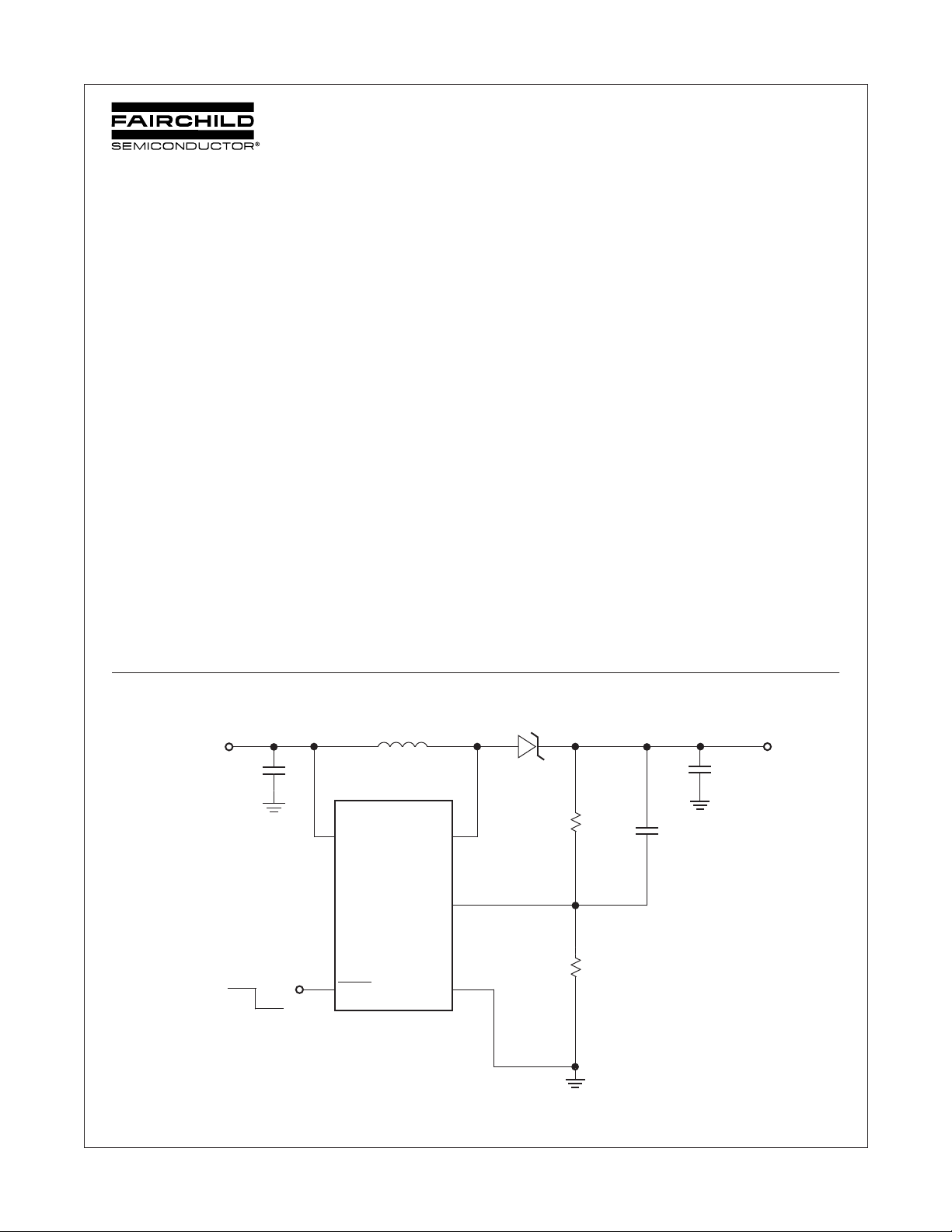
Typical Application
C
IN
4.7µF
2.7V to 5.5V
VIN
L
10µH
Description
The FAN5331 is a general purpose, fixed-frequency boost converter designed to operate at high switching frequencies in
order to minimize switching noise measured at the battery terminal of hand-held communications equipment. Quiescent current in normal mode of operation as well as in shutdown mode
is designed to be minimal in order to extend battery life. Normal
mode of operation or shutdown mode can be selected by a logic
level shutdown circuitry.
The low ON-resistance of the internal N-channel switch ensures
high efficiency and low power dissipation. A cycle-by-cycle current limit circuit keeps the peak current of the switch below a
typical value of 1A. The FAN5331 is available in a 5-lead SOT23 package.
BAT54
C
OUT
4.7µF
V
OUT
ON
OFF
©2004 Fairchild Semiconductor Corporation
FAN5331 Rev. 1.0.1
5
V
IN
1
SW
3
FB
R1
FAN5331
R2
4
SHDN
GND
2
Figure 1. Typical Application Diagram
1
C
F
120pF
www.fairchildsemi.com
Page 2
Pin Assignment
FAN5331 High Efficiency Serial LED Driver and OLED Supply with 20V Integrated Switch
Top View
SW
V
IN
GND
FB
SHDN
5-Lead SOT-23
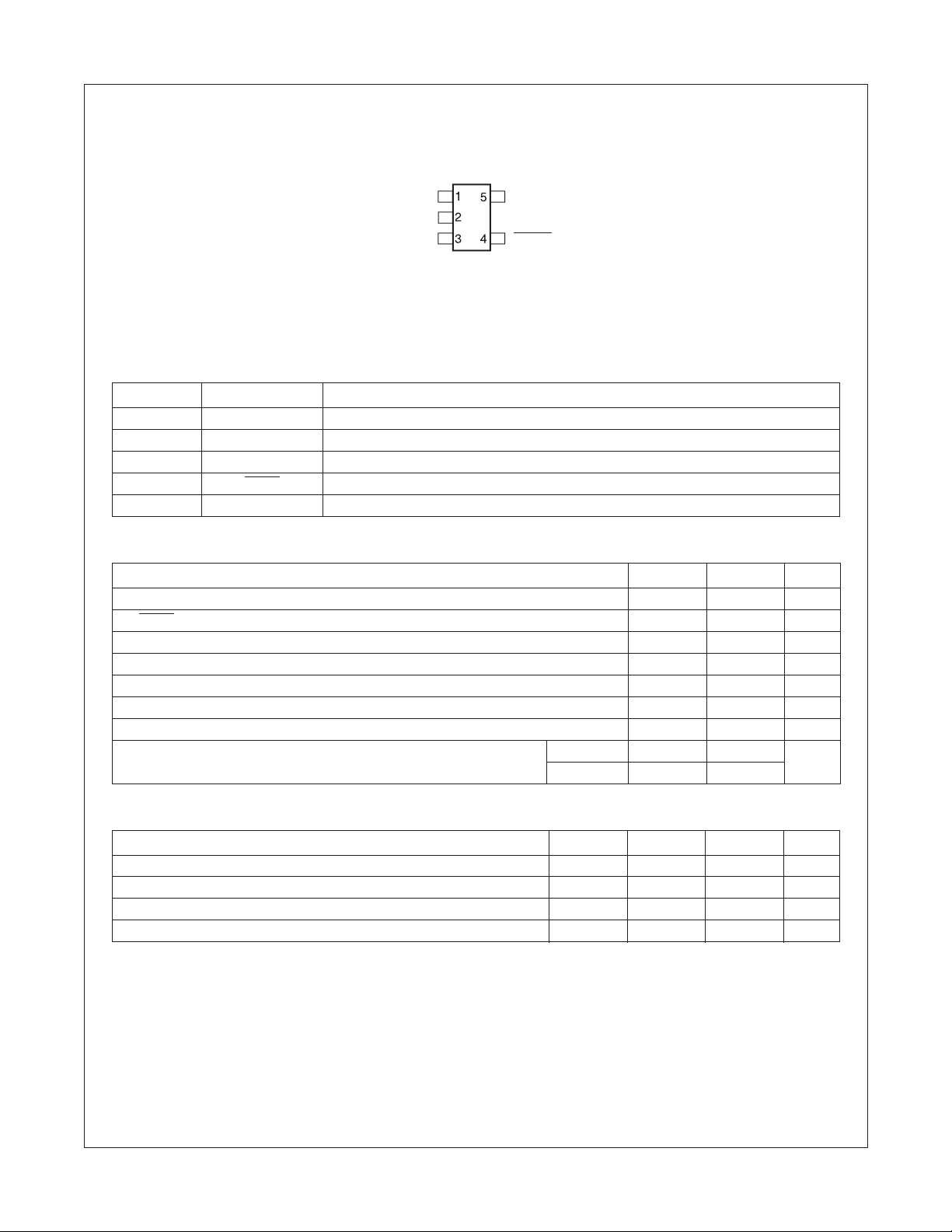
Figure 2. Pin Assignment
Pin Description
Pin No. Pin Name Pin Description
1SWSwitching node.
2 GND Analog and power ground.
3FBFeedback node that connects to an external voltage divider.
4 SHDN
5V
IN
Absolute Maximum Ratings (
V
to GND 6.0 V
IN
FB, SHDN
SW to GND -0.3 23 V
Lead Soldering Temperature (10 seconds) 300 °C
Junction Temperature 150 °C
Storage Temperature -55 150 °C
Thermal Resistance ( Θ
Electrostatic Discharge Protection (ESD) Level (Note 2) HBM 2.5 kV
to GND -0.3 V
) 265 °C/W
JA
Shutdown control pin. Logic HIGH enables, logic LOW disables the device.
Input voltage.
Note1)
Parameter Min Max Unit
+ 0.3 V
IN
CDM 1
Recommended Operating Conditions
Parameter Min Typ Max Unit
Input Voltage 2.7 5.5 V
Output Voltage V
Operating Ambient Temperature -40 25 85 °C
Output Capacitance (Note 3) 1.6 µF
IN
Notes:
1. Stresses above those listed under “Absolute Maximum Ratings” may cause permanent damage to the device. This
is a stress rating only and functional operation of the device at these or any other conditions above those indicated
in the operational section of this specification is not implied. Exposure to absolute maximum rating conditions for
extended periods may affect device reliability. Absolute maximum ratings apply individually only, not in combination.
2. Using EIA/JESD22A114B (Human Body Model) and EIA/JESD22C101-A (Charge Device Model).
3. This load capacitance value is required for the loop stability. Tolerance, temperature variation, and voltage
dependency of the capacitance must be considered. Typically a 4.7µF ceramic capacitor is required to achieve
specified value at V
FAN5331 Rev. 1.0.1
OUT
= 15V.
2
20 V
www.fairchildsemi.com
Page 3
≥
≥
Ω
Ω
µ
µ
Electrical Characteristics
Unless otherwise noted, V
Figure 3.
Parameter Conditions Min. Typ. Max. Units
Switch Current Limit V
Load Current Capability V
Switch On-resistance V
Quiescent Current V
OFF Mode Current V
Shutdown Threshold Device ON 1.5 V
Shutdown Pin Bias Current V
Feedback Voltage I
Feedback Pin Bias Current 10 nA
Feedback Voltage Line Regulation 2.7V < V
Switching Frequency 1.15 1.6 1.85 MHz
Maximum Duty Cycle 87 93 %
Enable Delay V
Power on Delay V
Switch Leakage Current No Switching, V
= 3.6V, T
IN
V
V
V
= -40°C to +85°C, Typical values are at T
A
= 3.2V 0.7 1 A
IN
= 15V, V
OUT
= 15V, V
OUT
= 5V 0.5
IN
= 3.6V 0.7
IN
= 3.6V, No Switching 0.7 mA
SHDN
= 3.6V, Switching 1.6 3.0 mA
SHDN
= 0V 0.1 2
SHDN
2.7V 35 mA
IN
3.2V 50 mA
IN
= 25°C, Test Circuit,
A
Device OFF 0.5 V
= 0V or V
SHDN
= 0mA 1.205 1.230 1.255 V
Load
< 5.5V, I
IN
= 2.7V, I
IN
= 2.7V, I
IN
OUT
OUT
= 5.5V 10 nA
SHDN
= 0mA 0.6 1.2 %
LOAD
= 35mA, V
= 35mA, V
= 5.5V 1
IN
= 15V 0.8 5 mS
OUT
= 15V 0.8 5 mS
OUT
FAN5331 High Efficiency Serial LED Driver and OLED Supply with 20V Integrated Switch
A
A
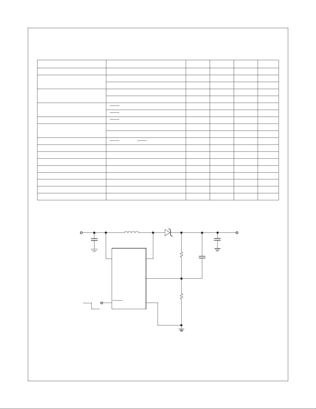
Test Circuit
VIN
C
IN
4.7µF
ON
2.7V to 5.5V
OFF
5
4
V
IN
SHDN
L
10µH
SW
FB
BAT54
1
3
FAN5331
2
GND
Figure 3. Test Circuit
R1
R2
150KΩ
13.4KΩ
C
F
120pF
C
OUT
4.7µF
V
OUT
FAN5331 Rev. 1.0.1
3
www.fairchildsemi.com
Page 4
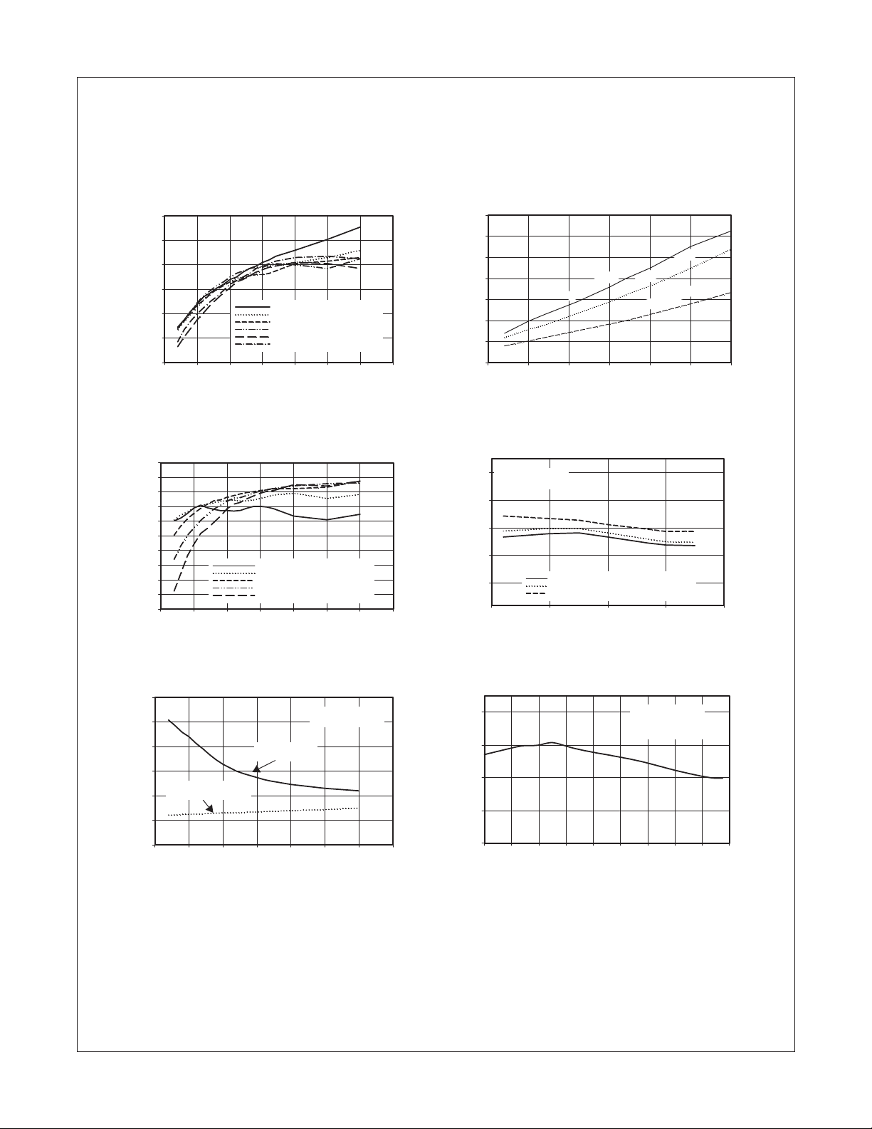
Typical Performance Characteristics
T
= 25°C, Test Circuit Figure 3, unless otherwise noted.
A
FAN5331 High Efficiency Serial LED Driver and OLED Supply with 20V Integrated Switch
Output Voltage vs Input Voltage
14.98
14.96
14.94
14.92
14.90
Output Voltage (V)
14.88
14.86
2.5 3.0 3.5 4.0 4.5 5.0 5.5 6.0
VIN(V) vs VOUT(V) at Iload=0mA
VIN(V) vs VOUT(V), at load=10mA
VIN(V) vs VOUT(V), at load=20mA
VIN(V) vs VOUT(V) at Iload=30mA
VIN(V) vs VOUT(V) at Iload=40mA
VIN(V) vs VOUT(V) at Iload=50mA
Input Voltage (V)
Efficiency vs Input Voltage
0.92
0.90
0.88
0.86
0.84
0.82
0.80
Efficiency
0.78
0.76
0.74
0.72
2.5 3.0 3.5 4.0 4.5 5.0 5.5 6.0
VIN(V) vs Efficiency at Iload = 10mA
VIN(V) vs Efficiency at Iload = 20mA
VIN(V) vs Efficiency at Iload = 30mA
VIN(V) vs Efficiency at Iload = 40mA
VIN(V) vs Efficiency at Iload = 50mA
Input Voltage (V)
Maximum Load Current vs Input Voltage
210
300
180
250
150
200
120
150
90
100
60
50
30
Maximum Load Current (mA)
0
0
2.5 3.0 3.5 4.0 4.5 5.0 5.5
2.5 3.0 3.5 4.0 4.5 5.0 5.5
V
V
2
1
=
T
U
O
V
V
15
=
T
U
O
O
V
V
1
2
=
T
U
Input Voltage (V)
Feedback Voltage vs Ambient Temperature
1.25
I
= 15mA
OUT
1.24
1.23
1.22
1.21
Feedback Voltage (V)
-50 0 50 100 150
Temperature (°C) vs Vf (Vin=2.7 V, Iload=15mA)
Temperature (°C) vs Vf (Vin=3.6 V, Iload=15mA)
Temperature (°C) vs Vf (Vin=5.5 V, Iload=15mA)
Ambient Temperature (°C)
Supply Current vs Input Voltage
3.0
2.5
2.0
1.5
1.0
0.5
Supply Current (mA)
0.0
2.5 3.0 3.5 4.0 4.5 5.0 5.5 6.0
FAN5331 Rev. 1.0.1
Non Switching
Switching
Input Voltage (V)
I
OUT
= 0mA
Switching Frequency vs Ambient Temperature
I
= 15mA
1.8
1.6
1.4
1.2
Switching Frequency (MHz)
1.0
-40 -20 0 20 40 6080100 120140
Ambient Temperature (°C)
4
OUT
V
= 15V
OUT
VIN = 3.6V
www.fairchildsemi.com
Page 5
FAN5331 High Efficiency Serial LED Driver and OLED Supply with 20V Integrated Switch
Typical Performance Characteristics
T
= 25°C, Test Circuit Figure 3, unless otherwise noted.
A
(Contd.)
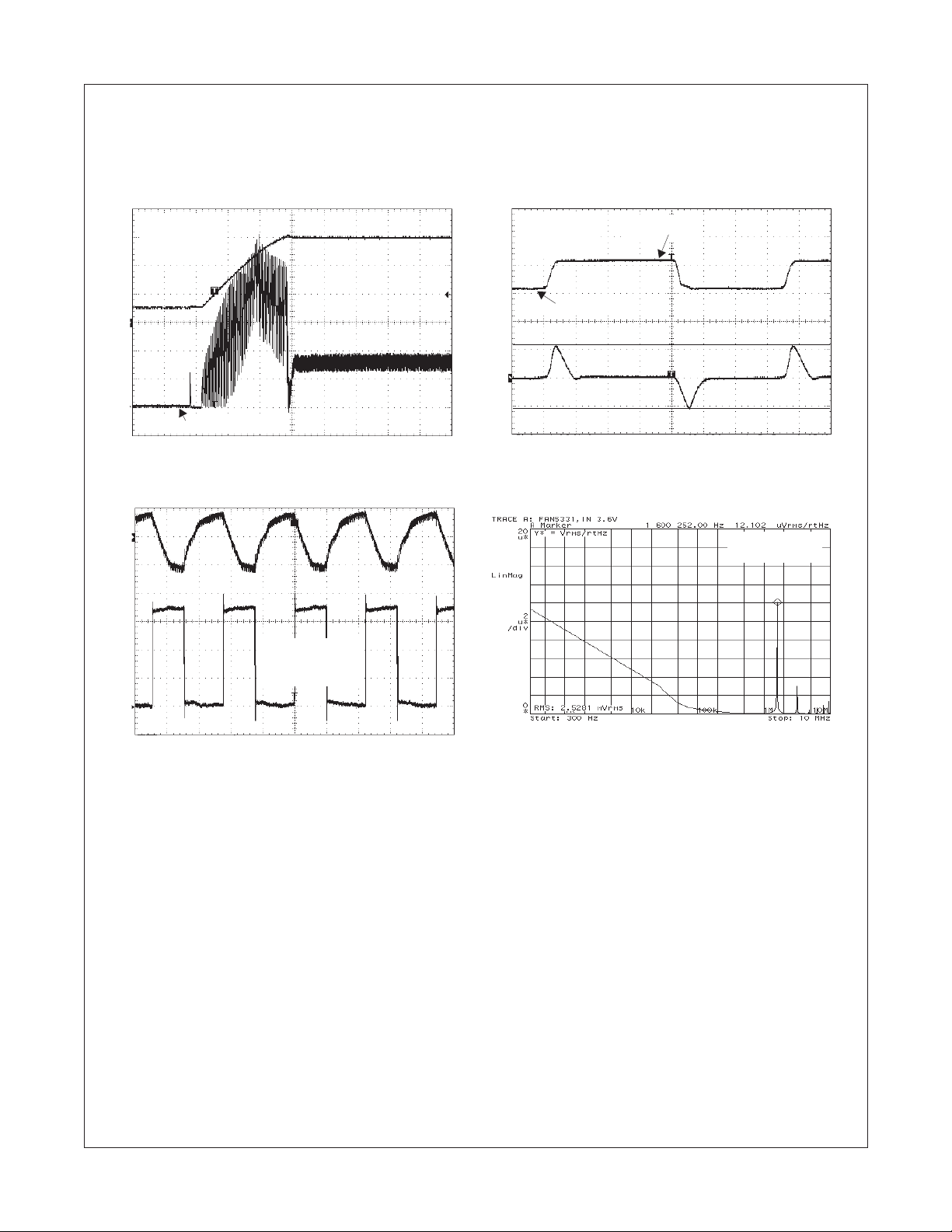
Startup After Enable
RL = 300
VIN = 3V
V
(5V/div)
(200mA/div)
Inductor Current= 0mA
OUT
Ω
= 15V
Time (200µs/div)
Load Transient Response
(100mV/Div)
Output Voltage Input Voltage
I
= 30mA
OUT
T
= Tf = 10µS
r
V
= 15V
OUT
VIN = 3.2V
Line Transient Response
VIN = 4.2V
Time (100µs/div)
Output Power Spectral Density
VIN = 3.6V
I
= 35mA
OUT
+0.6V
-0.6V
(10mA/Div)
Tr = Tf < 1µS
= 15V
V
OUT
I
= 0 to 35mA
OUT
Time (20µs/div)
FAN5331 Rev. 1.0.1
5
www.fairchildsemi.com
Page 6
Block Diagram
FB
FAN5331 High Efficiency Serial LED Driver and OLED Supply with 20V Integrated Switch
V
+
Over
Voltage
Comp
-
IN
+
Comp
-
Current Limit
Comparator
Soft-Start
SW
1
R
Amp
n
+
0.05
-
Q
R
R
S
+-
Driver
SHDN
45
Shutdown
Circuitry
3
1.15 x V
-
Error
Amp
+
FB
REF
Shutdown
Thermal
S
Ramp
Generator
Oscillator
Reference
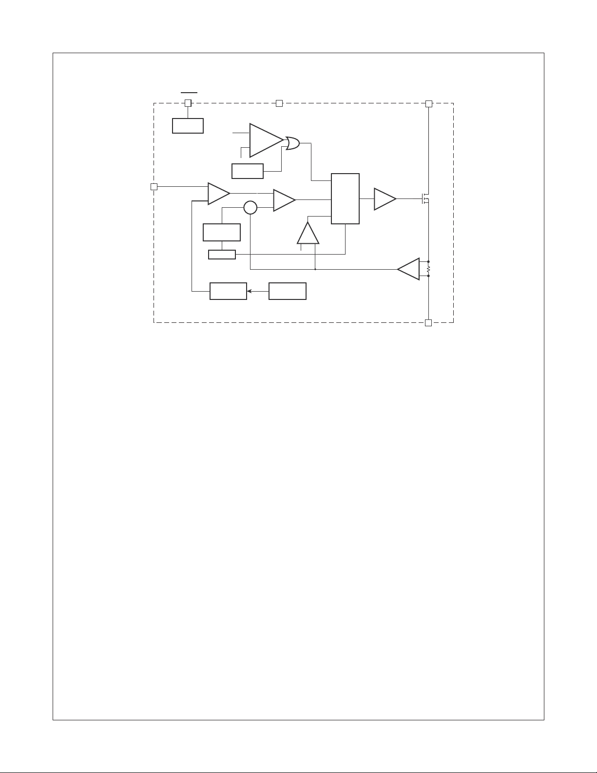
Figure 4. Block Diagram
Circuit Description
The FAN5331 is a pulse-width modulated (PWM) current-mode
boost converter. The FAN5331 improves the performance of battery powered equipment by significantly minimizing the spectral
distribution of noise at the input caused by the switching action of
the regulator. In order to facilitate effective noise filtering, the
switching frequency was chosen to be high, 1.6MHz. An internal
soft start circuitry minimizes in-rush currents. The timing of the soft
start circuit was chosen to reach 95% of the nominal output voltage
within maximum 5mS following an enable command when V
2.7V, V
OUT
= 15V, I
= 35mA and C
LOAD
OUT (EFFECTIVE)
The device architecture is that of a current mode controller with
an internal sense resistor connected in series with the N-channel switch. The voltage at the feedback pin tracks the output
voltage at the cathode of the external Schottky diode (shown in
the test circuit). The error amplifier amplifies the difference
between the feedback voltage and the internal bandgap reference. The amplified error voltage serves as a reference voltage
to the PWM comparator. The inverting input of the PWM comparator consists of the sum of two components: the amplified
control signal received from the 50m Ω current sense resistor
and the ramp generator voltage derived from the oscillator. The
oscillator sets the latch, and the latch turns on the FET switch.
Under normal operating conditions, the PWM comparator resets
the latch and turns off the FET, thus terminating the pulse.
Since the comparator input contains information about the output voltage and the control loop is arranged to form a negative
feedback loop, the value of the peak inductor current will be
adjusted to maintain regulation.
Every time the latch is reset, the FET is turned off and the current flow through the switch is terminated. The latch can be
= 3.2 µ F.
IN
2
GND
reset by other events as well. Over-current condition is monitored by the current limit comparator which resets the latch and
turns off the switch instantaneously within each clock cycle.
Over-Voltage Protection
The voltage on the feedback pin is sensed by an OVP Comparator. When the feedback voltage is 15% higher than the nominal
voltage, the OVP Comparator stops switching of the power transistor, thus preventing the output voltage from going higher.
=
Applications Information
Setting the Output Voltage
The internal reference is 1.23V (Typical). The output voltage is
divided by a resistor divider, R1 and R2 to the FB pin. The output voltage is given by
R
1
V
OUT
=
V
+
1
REF
-------
R
2
According to this equation, and assuming desired output voltage of 15V, good choices for the feedback resistors are,
R
=150k Ω and R
1
=13.4k Ω .
2
Inductor Selection
The inductor parameters directly related to device performances
are saturation current and dc resistance. The FAN5331 operates with a typical inductor value of 10µH. The lower the dc
resistance, the higher the efficiency. Usually a trade-off between
inductor size, cost and overall efficiency is needed to make the
optimum choice.
FAN5331 Rev. 1.0.1
6
www.fairchildsemi.com
Page 7
FAN5331 High Efficiency Serial LED Driver and OLED Supply with 20V Integrated Switch
The inductor saturation current should be rated around 1A,
which is the threshold of the internal current limit circuit. This
limit is reached only during the start-up and with heavy load
condition; when this event occurs the converter can shift over in
discontinuous conduction mode due to the automatic turn-off of
the switching transistor, resulting in higher ripple and reduced
efficiency.
Some recommended inductors are suggested in the table
below:
Inductor
Value Vendor Part Number Comment
10µH Panasonic ELL6GM100M Lower Profile
(1.6mm)
10µH Murata LQS66SN100M03L Highest
Efficiency
10µH Coilcraft DO1605T-103Mx Small Size
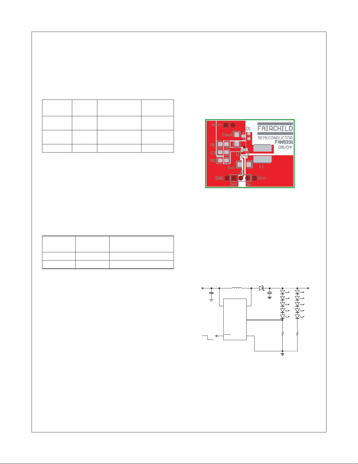
Table 1: Recommended Inductors
Capacitors Selection
For best performance, low ESR input and output capacitors are
required. Ceramic capacitors in the range 4.7µF to 10µF, placed
as close to the IC pins, are recommended for the lower input
and output ripple. The output capacitor voltage rating should be
according to the V
A feed forward capacitor C
mended value (R
suggested in the table below.
Capacitor
Value Vendor Part Number
4.7µF Panasonic ECJ3YB1C475K
4.7µF Murata GRM31CR61C475
setting.
OUT
, is required for stability. The recom-
F
x C
) is around 18µS. Some capacitors are
1
F
PCB Layout Recommendations
The inherently high peak currents and switching frequency of
power supplies require careful PCB layout design. Therefore,
use wide traces for high current paths and place the input
capacitor, the inductor, and the output capacitor as close as
possible to the integrated circuit terminals. The resistor divider
that sets the output voltage should be routed away from the
inductor to avoid RF coupling. A four layer PCB with at least one
ground plane connected to the pin 2 of the IC is recommended.
This ground plane acts as an electromagnetic shield to reduce
EMI and parasitic coupling between components.
Figure 5. Recommended Layout
Application Examples
1. LED Driver
One or more serial LED strings can be driven with a constant
current, set by the series resistor, given by
1.23V
LED
----------------=
R1
I
Table 2: Recommended Capacitors
Diode Selection
The external diode used for rectification is usually a Schottky
diode. Its average forward current and reverse voltage maximum ratings should exceed the load current and the voltage at
the output of the converter respectively. A barrier Schottky diode
such as BAT54 is preferred, due to its lower reverse current over
the temperature range.
Care should be taken to avoid any short circuit of V
OUT
even with the IC disabled, since the diode can be instantly damaged by the excessive current.
Thermal Shutdown
When the die temperature exceeds 150°C, a reset occurs and
will remain in effect until the die cools to 130°C, at that time the
circuit will be allowed to restart.
FAN5331 Rev. 1.0.1
to GND,
VIN
C
ON
IN
4.7µF
2.7V to 5.5V
OFF
GND
BAT54
C
OUT
4.7µF
1
SW
3
FB
2
R1
L
10µH
5
4
V
IN
SHDN
5331
AN
F
V
OUT
R2
Figure 6. Low Noise Boost LED Driver
7
www.fairchildsemi.com
Page 8
FAN5331 High Efficiency Serial LED Driver and OLED Supply with 20V Integrated Switch
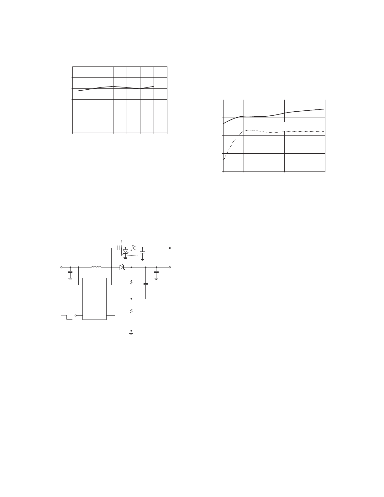
LED Current vs Input Voltage
(String Connected to FB Pin)
20.2
20.1
20.0
19.9
19.8
LED Current (mA)
19.7
2.5 3.0 3.54.04.55.05.56.0
Input Voltage (V)
The feedback loop tightly regulates the current in the branch
connected to FB pin, while the current in the other branch
depends on the sum of the LED’s forward voltages, V
OUT
and
the ballast resistor. The input and the output ripple is less than
3mV
A Zener diode (VZ = 22V) connected between V
, for load currents up to 40mA.
RMS
OUT
and GND
can prevent the FAN5331 from being damaged by over-voltage,
if the load is accidently disconnected during operation.
2. Dual Boost Converter
A negative voltage can be provided by adding an external
charge pump (C1, C2, D2, and D3).
While the feedback loop tightly regulates V
put voltage (-V
) can supply a light load with a negative volt-
OUT
, the negative out-
OUT
age. Nevertheless, the negative voltage depends on the
changes of the load current in both -V
OUT
and +V
, as shown
OUT
in the graph below.
Negative Output Voltage vs Load Current
-18
-15V/Unloaded
-16
-15V/10mA Load
-14
-12
Negative Output Voltage (V)
-10
01020304050
Load Current On Positive Output Side (mA)
BAT54S
C1
D2
0.1µF
D3
4.7µF
2.7V to 5.5V
V
IN
C
IN
4.7µF
ON
OFF
L
10µH
5
V
IN
AN5331
F
4
SHDN
BAT54
D1
R1
1
SW
3
FB
R2
2
GND
Figure 7. Dual (±) Boost Converter
C2
C
120pF
-V
OUT
I
= 10mA
OUT
V
OUT
C
OUT
I
= 50mA
OUT
4.7µF
F
FAN5331 Rev. 1.0.1
8 www.fairchildsemi.com
Page 9
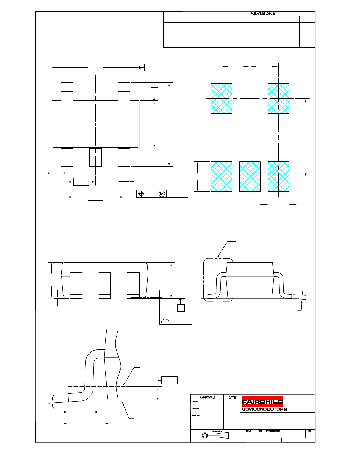
3.00
2.80
RELEASE TO DOCUMENT CONTROL
A
REDRAW PER CURRENT STANDARD
B
REDRAW AS PER JEDEC NEW ISSUE FROM A TO
C
B. CHANGE DRAWING TEMPLATE FROM
LANDSCAPE TO PORTRAIT. CHANGE DIMENSION
UNIT FROM INCHES TO MILLIMETERS.
CHANGED BOTTOM VIEW TO TOP VIEW,
4 27 JUNE 07 L.HUEBENER
REMOVED DATE FROM NOTES, ADDED NOTE C,
CHANGED FONT STYLE
5
BODY THICKNESS, TERMINAL THICKNESS, PACKAGE HEIGHT ADJUSTED TO MEET JEDEC STD
DESCRIPTIONLTR
DATE
E.C.N. BY/APP'D
12/07/95
11208
11531
07/31/96
17 JULY 07
TL
LUA
L.HUEBENER
SYMM
C
L
A
0.950.95
(0.30)
5
4
B
3.00
2.60
1.70
1.50
1
0.95
1.90
32
0.50
1.00
0.30
0.20 C A B
2.60
0.70
TOP VIEW
LAND PATTERN RECOMMENDATION
SEE DETAIL A
1.30
0.90
0.15
0.05
8°
0°
0.55
0.35
0.60 REF
1.45 MAX
0.10
GAGE PLANE
0.25
SEATING PLANE
C
C
NOTES: UNLESS OTHEWISE SPECIFIED
A) THIS PACKAGE CONFORMS TO JEDEC
MO-178, ISSUE B, VARIATION AA,
B) ALL DIMENSIONS ARE IN MILLIMETERS.
C) MA05Brev5
L.HUEBENER
H.ALLEN
17 JULY 07
19 JULY 07
MM
0.22
0.08
5LD,SOT23,JEDEC
MO-178,1.6MM
NA
NA
FORMERLY: N/A OF
MKT-MA05B
SHEET : 1 1
5
Page 10
®
®
®
TRADEMARKS
The following includes registered and unre gistered trademarks and service ma rks, owned by Fairchild Semicondu ctor and/or i ts global subsidiarie s, and is not
intended to be an exhaustive list of all such trademarks.
2Cool
AccuPower
AX-CAP*
BitSiC
Build it Now
CorePLUS
CorePOWER
CROSSVOLT
CTL
Current Transfer Logic
DEUXPEED
Dual Cool™
EcoSPARK
®
®
EfficientMax
ESBC
®
Fairchild
Fairchild Semiconductor
FACT Quiet Series
®
FACT
®
FAST
FastvCore
FETBench
FlashWriter
®
*
FPS
F-PFS
®
FRFET
Global Power ResourceSM
GreenBridge
Green FPS
Green FPS e-Series
Gmax
GTO
IntelliMAX
ISOPLANAR
Making Small Speakers Sound Louder
and Better™
MegaBuck
MICROCOUPLER
MicroFET
MicroPak
MicroPak2
®
MillerDrive
MotionMax
Motion-SPM
mWSaver
OptoHiT
OPTOLOGIC
OPTOPLANAR
®
®
®
PowerTrench
PowerXS™
Programmable Active Droop
®
QFET
QS
Quiet Series
RapidConfigure
Saving our world, 1mW/W/kW at a time™
SignalWise
SmartMax
SMART START
Solutions for Your Success
®
SPM
STEALTH
SuperFET
®
SuperSOT-3
SuperSOT-6
SuperSOT-8
SupreMOS
®
SyncFET
Sync-Lock™
®
*
The Power Franchise
TinyBoost
TinyBuck
TinyCalc
®
TinyLogic
TINYOPTO
TinyPower
TinyPWM
TinyWire
TranSiC
TriFault Detect
TRUECURRENT
®
*
SerDes
®
UHC
Ultra FRFET
UniFET
VCX
VisualMax
VoltagePlus
XS™
* Trademarks of System General Corporation, used under license by Fairchild Semiconductor.
DISCLAIMER
FAIRCHILD SEMICONDUCTOR RESERVES THE RIGHT TO MAKE CHANGES WITHOUT FURTHER NOTICE TO ANY PRODUCTS HEREIN TO IMPROVE
RELIABILITY, FUNCTION, OR DESIGN. FAIRCHILD DOES NOT ASSUME ANY LIABILITY ARISING OUT OF THE APPLICATION OR USE OF ANY PRODUCT
OR CIRCUIT DESCRIBED HEREIN; NEITHER DOES IT CONVEY ANY LICENSE UNDER ITS PATENT RIGHTS, NOR THE RIGHTS OF OTHERS. THESE
SPECIFICATIONS DO NOT EXPAND THE TERMS OF FAIRCHILD’S WORLDWIDE TERMS AND CON DITIONS, SPECIFICALLY THE WARRANTY THEREIN,
WHICH COVERS THESE PRODUCTS.
LIFE SUPPORT POLICY
FAIRCHILD’S PRODUCTS ARE NOT AUTHORIZED FOR USE AS CRITICAL COMPONENTS IN LIFE SUPPORT DEVICES OR SYSTEMS WITHOUT THE
EXPRESS WRITTEN APPROVAL OF FAIRCHILD SEMICONDUCTOR CORPORATION.
As used herein:
1. Life support devices or systems are devices or systems which, (a)
are intended for surgical implant into the body or (b) support or
sustain life, and (c) whose failure to perform when properly used in
accordance with instructions for use provided in the labeling, can be
reasonably expected to result in a significant injury of the user.
2. A critical component in any component of a life support, device, or
system whose failure to perform can be reasonably expected to
cause the failure of the life support device or system, or to affect its
safety or effectiveness.
ANTI-COUNTERFEITING POLICY
Fairchild Semiconductor Corporation's Anti-C ounterfe iting Policy . Fairchild' s Anti-C ounterfei ting Poli cy is also sta ted on ou r external w ebsite, w ww.fair childsemi .com,
under Sales Support.
Counterfeiting of semiconductor parts is a grow ing problem in t he industry. Al l manufa cturers of semiconducto r produ cts are e xperiencing counterfeiting of their
parts. Customers who inadvertently purchase counter feit parts ex perience many problem s such as lo ss of bra nd repu tation, su bstandar d performance, failed
applications, and increased cost of production and manu facturing delays. Fair child i s taking strong measures to protect our selv es and our custome rs from the
proliferation of counterfeit parts. Fairchild stron gly encourag es customers to pur chase Fairchild parts eith er directly from Fai rchild or fr om Authorize d Fairchild
Distributors who are listed by country on our web page cited above. Products customers buy either from Fairchild directly or from Authorized Fairchild Distributors
are genuine parts, have full tr aceability , meet Fairchild's quality stan dards for handling an d storage and pro vide access to Fairchild's full range of up-to-date technical
and product information. Fairchil d and o ur Author ized Distributo rs will stan d behind all warran ties and will a ppropriately address any warranty issues that may ari se.
Fairchild will not provide any w arranty cov erage or other assi stance for parts bought from Unauthor ized Sour ces. Fair child is committed to combat this global
problem and encourage our customers to do their part in stopping this practi ce by bu ying dire ct or from authori zed distribu tors.
PRODUCT STATUS DEFINITIONS
Definition of Terms
Datasheet Identification Product Status Definition
Advance Information Formative / In Design
Preliminary First Production
No Identification Needed Full Production
Obsolete Not In Production
Datasheet contains the design specifications for product development. Specifications may change
in any manner without notice.
Datasheet contains preliminary data; supplementary data will be published at a later date. Fairchild
Semiconductor reserves the right to make changes at any time without notice to improve design.
Datasheet contains final specifications. Fairchild Semiconductor reserves the right to make
changes at any time without notice to improve the design.
Datasheet contains specifications on a product that is discontinued by Fairchild Semiconductor.
The datasheet is for reference information only.
Rev. I61
© Fairchild Semiconductor Corporation www.fairchildsemi.com
 Loading...