

查询FAN5099供应商
FAN5099 Wide Frequency Synchronous Buck
PWM & LDO Controller
FAN5099 Wide Frequency Synchronous Buck PWM & LDO Controller
Decemeber 2006
Features
■ General Purpose PWM Regulator and LDO Controller
■ Input Voltage Range: 3V to 24V
■ Output Voltage Range: 0.8V to 15V
■ V
CC
– 5V
– Shunt Regulator for 12V Operation
■ Support for Ceramic Cap on PWM Output
■ Programmable Current Limit for PWM Output
■ Wide Programmable Switching Frequency Range
(50kHz to 600kHz)
■ R
■ Internal Synchronous Boot Diode
■ Soft-Start for both PWM and LDO
■ Multi-Fault Protection with Optional Auto-restart
■ 16-Pin TSSOP Package
Current Sensing
DS(ON)
Applications
■ High-Efficiency (80+) Computer Power Supplies
■ PC/Server Motherboard Peripherals
– V
_MCH (1.5V), V
CC
V
■ Power Supply for
– FPGA, DSP, Embedded Controllers, Graphic Card
Processor, and Communication Processors
■ High-Power DC-to-DC Converters
TT_GTL
(1.25V)
(1.5V) and
DDQ
Related Application Notes
■ AN-6020 FAN5099 Component Calculation and
Simulation Tools
■ AN-6005 Synchronous Buck MOSFET Loss
Calculations with Excel Model
Description
The FAN5099 combines a high-efficiency pulse-width
modulated (PWM) controller and an LDO (Low DropOut)
linear regulator controller. The PWM controller is
designed to operate over a wide frequency range (50kHz
to 600kHz) to accommodate a variety of applications.
Synchronous rectification provides high efficiency over a
wide range of load currents. Efficiency is further
enhanced by using the low-side MOSFET’s R
sense current. In addition, the capability to operate at low
switching frequencies provides opportunities to boost
power supply efficiency by reducing switching losses and
gain cost savings using low-cost materials, such as powdered iron cores, on the output inductor.
Both the linear and PWM regulator soft-start are controlled by a single external capacitor, to limit in rush current from the supply when the regulators are first
enabled. Current limit for PWM is also programmable.
The FAN5099’s ability to handle wide input voltage
ranges makes this controller suitable for power solutions
in a wide range of applications involving conversion input
voltages from Silver box, battery, and adapters. The
PWM regulator employs a summing-current-mode control with external compensation to achieve fast load transient response and provide system design optimization.
FAN5099 is offered in both industrial temperature grade
(-40°C to +85°C) as well as commercial temperature
grade (-10°C to +85°C).
DS(ON)
to
Ordering Information
Part Number Operating Temp. Range Pb-Free Package Packing Method Qty/Reel
FAN5099MTCX -10°C to +85°C Yes 16-Lead TSSOP Tape and Reel 2500
FAN5099EMTCX -40°C to +85°C Yes 16-Lead TSSOP Tape and Reel 2500
FAN5099MX -10°C to +85°C Yes 16-Lead SOIC Tape and Reel 2500
FAN5099EMX -40°C to +85°C Yes 16-Lead SOIC Tape and Reel 2500
Note: Contact Fairchild sales for availability of other package options.
© 2006 Fairchild Semiconductor Corporation www.fairchildsemi.com
FAN5099 Rev. 1.1.3
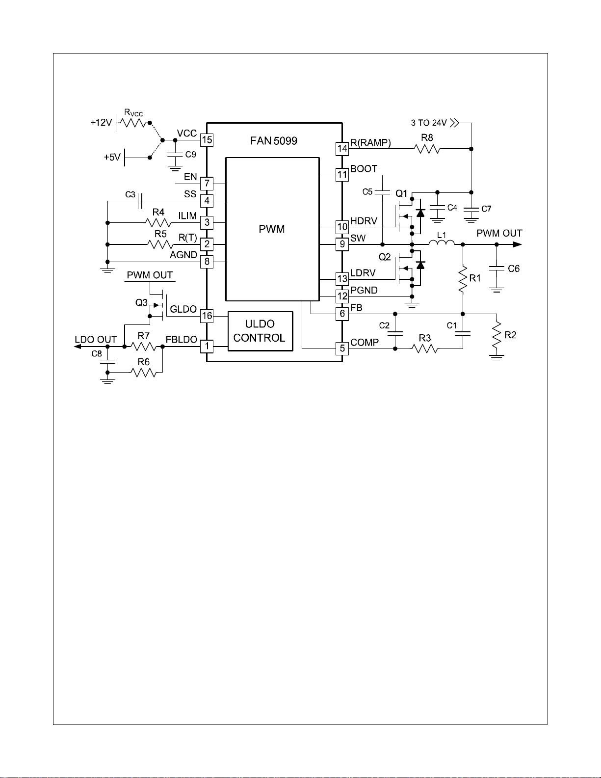
Typical Application
FAN5099 Wide Frequency Synchronous Buck PWM & LDO Controller
Figure 1. Typical Application Diagram
© 2006 Fairchild Semiconductor Corporation www.fairchildsemi.com
FAN5099 Rev. 1.1.3 2
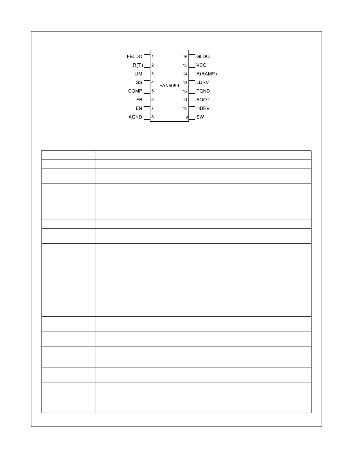
Pin Assignment
Figure 2. Pin Assignment
Pin Description
Pin No. Pin Name Pin Description
1FBLDOLDO Feedback. This node is regulated to V
2R(T)Oscillator Set Resistor. This pin provides oscillator switching frequency adjustment. By plac-
ing a resistor (RT) from this pin to GND, the nominal 50kHz switching frequency is increased.
3ILIMCurrent Limit. A resistor from this pin to GND sets the current limit.
4 SS Soft-Start. A capacitor from this pin to GND programs the slew rate of the converter and the
LDO during initialization. It also sets the time by which the converter delays when restarting
after a fault occurs. SS has to reach 1.2V before fault shutdown feature is enabled. The LDO
is enabled when SS reaches 2.2V.
5COMPCOMP. The output of the error amplifier drives this pin.
6FBFeedback. This pin is the inverting input of the internal error amplifier. Use this pin, in combi-
nation with the COMP pin, to compensate the feedback loop of the converter.
7ENEnable. Enables operation when pulled to logic high. Toggling EN resets the regulator after a
latched fault condition. This is a CMOS input whose state is indeterminate if left open and
needs to be properly biased at all times.
8AGND
9SWSwitching Node. Return for the high-side MOSFET driver and a current sense input. Connect
10 HDRV High-Side Gate Drive Output. Connect to the gate of the high-side power MOSFETs. This
11 BOO T Bootstrap Supply Input. Provides a boosted voltage to the high-side MOSFET driver.
12 PGND Power Ground. The return for the low-side MOSFET driver. Connect to source of low-side
13 LDRV Low-Side Gate Drive Output. Connect to the gate of the low-side power MOSFETs. This pin
14 R(RAMP) Ramp Resistor. A resistor from this pin to VIN sets the ramp amplitude and provides voltage
15 VCC V
16 GLDO Gate Drive for the LDO. Turned off (low) until SS is greater than 2.2V.
Analog Ground.
pin. Tie this pin to the ground island/plane through the lowest impedance connection available.
to source of high-side MOSFET and drain of low-side MOSFET.
pin is also monitored by the adaptive shoot-through protection circuitry to determine when the
high-side MOSFET is turned off.
Connect to bootstrap capacitor as shown in Figure 1.
MOSFET.
is also monitored by the adaptive shoot-through protection circuitry to determine when the
lower MOSFET is turned off.
feed-forward.
. Provides bias power to the IC and the drive voltage for LDRV. Bypass with a ceramic
CC
capacitor as close to this pin as possible. This pin has a shunt regulator which draws current
when the input voltage is above 5.6V.
The signal ground for the IC. All internal control voltages are referred to this
REF
.
FAN5099 Wide Frequency Synchronous Buck PWM & LDO Controller
© 2006 Fairchild Semiconductor Corporation www.fairchildsemi.com
FAN5099 Rev. 1.1.3 3
Absolute Maximum Ratings
The “Absolute Maximum Ratings” are those values beyond which the safety of the device cannot be guaranteed. The
device should not be operated at these limits. The parametric values defined in the Electrical Characteristics tables
are not guaranteed at the absolute maximum ratings. The “Recommended Operating Conditions” table defines the
conditions for actual device operation.
VCC to PGND 6.0 V
BOOT to PGND 33.0 V
SW to PGND Continuous -0.5 33.0 V
HDRV (V
– VSW) 6.0 V
BOOT
LDRV -0.5 6.0 V
All Other Pins -0.3 V
Maximum Shunt Current for V
Electrostatic Discharge (ESD) Protection
(2)
Level
Notes:
1. Stresses above those listed under “Absolute Maximum Ratings” may cause permanent damage to the device. This
is a stress rating only; functional operation of the device at these or any conditions above those indicated in the
operational section of this specification is not implied. Exposure to absolute maximum rating conditions for extended
periods may affect device reliability. Absolute maximum ratings apply individually only, not in combination. Unless
otherwise specified, all other voltages are referenced to AGND.
2. Using Mil Std. 883E, method 3015.7 (Human Body Model) and EIA/JESD22C101-A (Charge Device Model).
(1)
Parameter Min. Max. Unit
Transient (t < 50ns, f < 500kHz) -3.0 33.0 V
+ 0.3 V
CC
CC
HBM 3.5 kV
CDM 1.8
150 mA
FAN5099 Wide Frequency Synchronous Buck PWM & LDO Controller
Thermal Information
Symbols Parameter Min. Typ. Max. Unit
T
STG
T
L
P
D
θ
JC
θ
JA
3. Junction-to-ambient thermal resistance, θJA, is a strong function of PCB material, board thickness, thickness and
number of copper planes, number of vias used, diameter of vias used, available copper surface, and attached heat
sink characteristics.
Storage Temperature -65 150 °C
Lead Soldering Temperature, 10 Seconds 300 °C
Vapor Phase, 60 Seconds 215 °C
Infrared, 15 Seconds 220 °C
Power Dissipation, TA = 25°C 715 mW
Thermal Resistance – Junction-to-Case 37 °C/W
Thermal Resistance – Junction-to-Ambient
(3)
100 °C/W
Recommended Operating Conditions
Symbols Parameter Conditions Min. Typ. Max. Unit
V
CC
T
A
T
J
Supply Voltage VCC to GND 4.5 5.0 5.5 V
Ambient Temperature
Commercial -10 85 °C
Industrial -40 85 °C
Junction Temperature 125 °C
© 2006 Fairchild Semiconductor Corporation www.fairchildsemi.com
FAN5099 Rev. 1.1.3 4
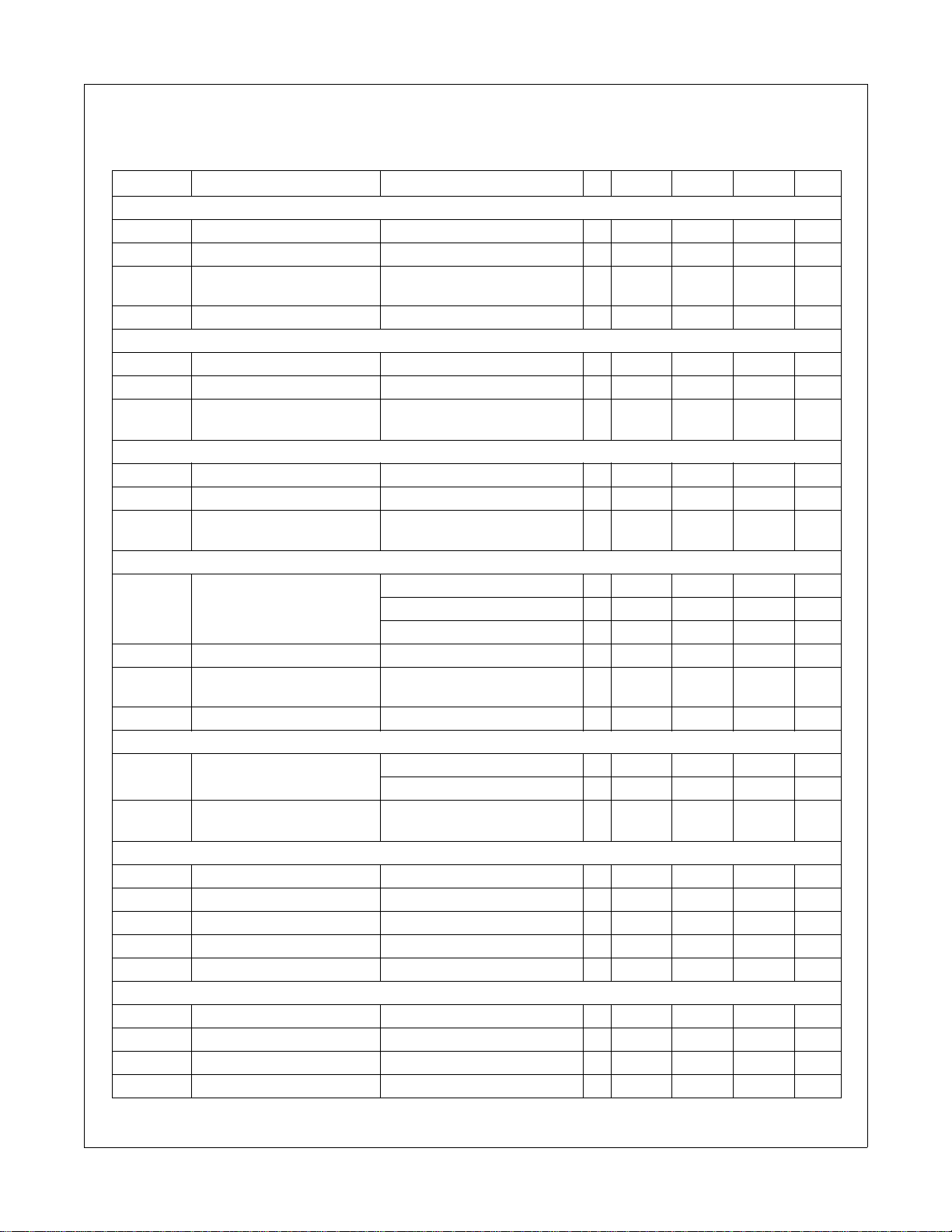
Electrical Characteristics
Unless otherwise noted, VCC = 5V, TA = 25°C, using the circuit in Figure 1. The ‘•’ denotes that the specifications apply
to the full ambient operating temperature range.
Symbol Parameter Conditions Min. Typ. Max. Unit
Supply Current
I
VCC
I
VCC(SD)VCC
I
VCC(OP)VCC
V
SHUNTVCC
Under-Voltage Lockout (UVLO)
UVLO(H) Rising V
UVLO(L) Falling V
Soft-Start
I
SS
V
LDOSTART
V
SSOK
Oscillator
F
OSC
ΔV
RAMP
Reference
V
REF
Error Amplifier
GBWP Gain-BW Product 25 MHz
S/R Slew Rate 10pF across COMP to GND 8 V/μS
I
FB
Gate Drive
R
HUP
R
HDN
R
LUP
R
LDN
VCC Current (Quiescent) HDRV, LDRV Open
Current (Shutdown) EN = 0V, VCC = 5.5V
Current (Operating)
Volta ge
UVLO Threshold
V
CC
(6)
UVLO Threshold
CC
UVLO Threshold
CC
Hysteresis
Current 10 μA
LDO Start Threshold 2.2 V
PWM Protection Enable
Threshold
Frequency
Operating Frequency Range 40 600 kHz
Ramp Amplitude
(Peak-to-Peak)
Minimum On Time f = 200kHz 200 ns
Reference Voltage
(Measured at FB Pin)
Current Amplifier Reference
(at SW node)
DC Gain 80 dB
Output Voltage Swing No Load
FB Pin Source Current μA
HDRV Pull-up Resistor Sourcing
HDRV Pull-down Resistor Sinking
LDRV Pull-up Resistor Sourcing
LDRV Pull-down Resistor Sinking
(4,5)
•
2.6 3.2 3.8 mA
EN = 5V, V
Q
= 20nC, FSW = 200kHz
FET
= 5.0V,
CC
Sinking 1mA to 100mA at VCC Pin
•
5.4 5.9 V
•
4.00 4.25 4.50 V
•
3.60 3.75 4.00 V
200 400 μA
10 15 mA
0.5 V
1.2 V
R(T) = 25.5KΩ ± 1% 240 300 360 kHz
R(T) = 199KΩ ± 1% 60 80 100 kHz
R(T) = Open 50 kHz
R(RAMP) = 330KΩ 0.4 V
TA = 0°C to 70°C
= -40°C to 85°C
T
A
•
790 800 810 mV
•
788 800 812 mV
160 mV
•
0.5 4.0 V
•
•
•
•
1.8 3.0 Ω
1.8 3.0 Ω
1.8 3.0 Ω
1.2 2.0 Ω
FAN5099 Wide Frequency Synchronous Buck PWM & LDO Controller
© 2006 Fairchild Semiconductor Corporation www.fairchildsemi.com
FAN5099 Rev. 1.1.3 5
Electrical Characteristics (Continued)
Unless otherwise noted, V
= 5V, T
CC
to the full ambient operating temperature range.
Symbol Parameter Conditions Min. Typ. Max. Unit
Protection/Disable
I
I
SWPD
V
V
Supply Current
TSD Thermal Shutdown 160 °C
V
Low Drop-Out (LDO)
V
LDOREF
V
LDO_DO
ILIMIT Source Current 9 10 11 μA
LIM
SW Pull-down Current SW = 1V, EN = 0V mA
Under-Voltage Threshold
UV
Over-Voltage Threshold
OV
Enable Threshold Voltage
EN
Enable Source Current V
Enable Sink Current
(7)
Reference Voltage
(measured at FBLDO pin)
Regulation 0A ≤ I
Drop-out Voltage I
External Gate Drive
Gate Drive Source Current 1.2 mA
Gate Drive Sink Current 400 μA
= 25°C, using the circuit in Figure 1. The ‘•’ denotes that the specifications apply
A
As % of set point;
2μS noise filter
As % of set point;
2μS noise filter
Enable Condition
Disable Condition
V
(4, 5)
65 75 80 %
•
110 115 120 %
•
•
2.0 V
•
= 5V 50 μA
CC
= 5V and fault conditions
CC
10 μA
0.8 V
(overload, short-circuit,
over-voltage, under-voltage)
TA = 0°C to 70°C
= -40°C to 85°C
T
A
≤ 5A
LOAD
≤ 5A and R
LOAD
= 4.75V
V
CC
= 5.6V
V
CC
< 50mΩ 0.3 V
DS-ON
•
775 800 825 mV
•
770 800 830 mV
•
1.17 1.20 1.23 V
•
•
4.5 V
5.3 V
FAN5099 Wide Frequency Synchronous Buck PWM & LDO Controller
Notes:
4. All limits at operating temperature extremes are guaranteed by design, characterization, and statistical quality control.
5. AC specifications guaranteed by design/characterization (not production tested).
6. For a case when V
is sinking current to keep voltage on V
7. Test Conditions: V
© 2006 Fairchild Semiconductor Corporation www.fairchildsemi.com
FAN5099 Rev. 1.1.3 6
is higher than the typical 5V V
CC
LDO_IN
= 1.5V and V
pin constant.
CC
LDO_OUT
voltage observed at VCC pin when the internal shunt regulator
CC,
= 1.2V.
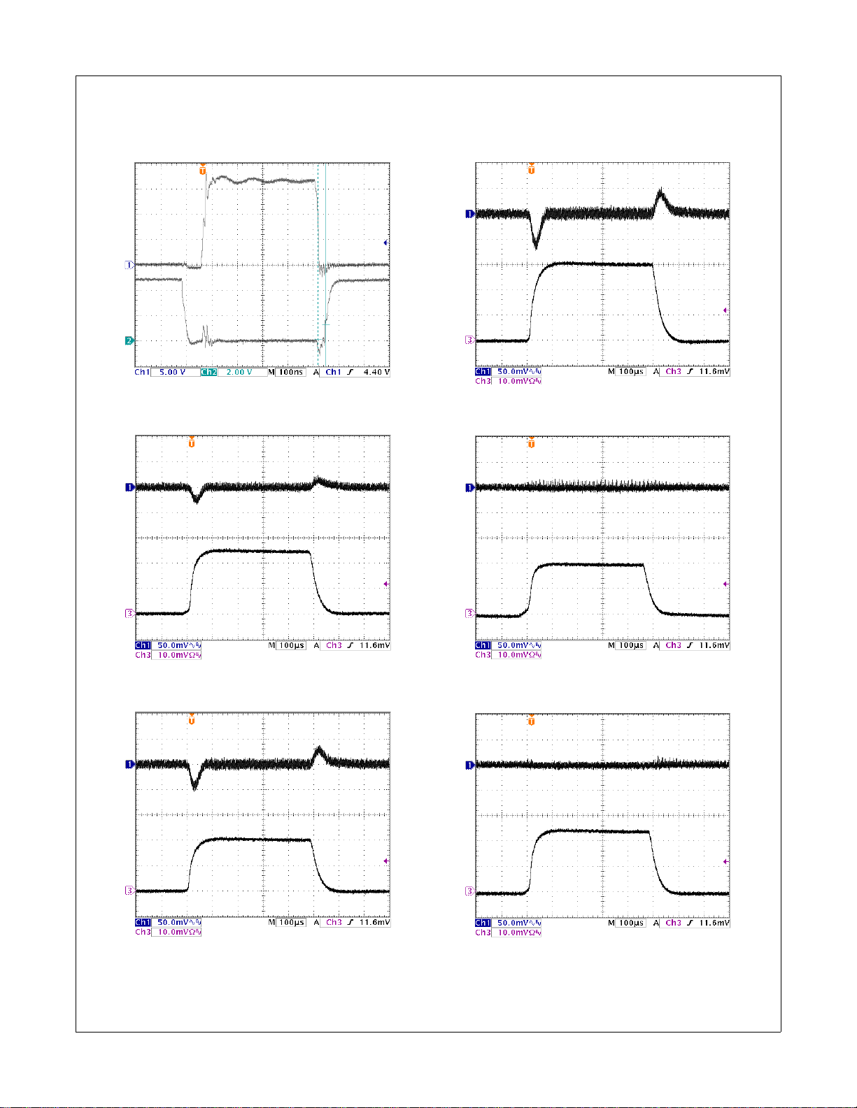
Typical Performance Characteristics
VIN=12V, Vdd=5V, V
OUT
=1.5V, V
=1.2V, I
ldo
load
=5A, I
ldo
=2A, F
= 300kHz, unless otherwise noted.
osc
FAN5099 Wide Frequency Synchronous Buck PWM & LDO Controller
Ch1: HDRV; Ch2: LDRV. Dead times: 62ns, 32ns
Figure 3. Dead Time Waveform
Ch1: V
; Ch3: IL, 2.5A/div
OUT
Figure 4. PWM Load Transient (0 to 5A)
Ch1: V
; Ch3: IL, 5A/div
OUT
Figure 6. PWM Load Transient (0 to 15A)
Ch1: V
OUT_LDO
; Ch3: I
LDO
, 1A/div
Figure 7. LDO Load Transient (0 to 2A)
Ch1: V
; Ch3: IL, 5A/div
OUT
Figure 5. PWM Load Transient (0 to 10A)
© 2006 Fairchild Semiconductor Corporation www.fairchildsemi.com
FAN5099 Rev. 1.1.3 7
Ch1: V
Figure 8. LDO Load Transient (0 to 5A)
OUT_LDO
; Ch3: I
LDO
, 2.5A/div
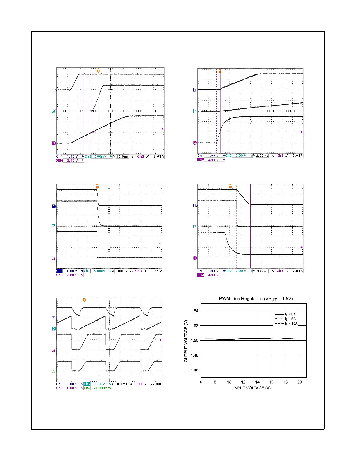
Typical Performance Characteristics (Continued)
VIN=12V, Vdd=5V, V
Ch1: V
; Ch2:V
OUT
OUT
OUT_LDO
=1.5V, V
; Ch3: SS
=1.2V, I
ldo
load
=5A, I
ldo
=2A, F
osc
= 300kHz, unless otherwise noted.
Ch1: V
; Ch2: SS; Ch3: EN
OUT
FAN5099 Wide Frequency Synchronous Buck PWM & LDO Controller
Figure 9. PWM/LDO Power Up
Ch1: V
OUT
; Ch2: V
OUT_LDO
; Ch3: SS
Figure 10. PWM/LDO Power Down
Figure 12. Enable On (I
Ch1: V
; Ch2: SS; Ch3: EN
OUT
Figure 13. Enable Off (I
PWM
PWM
= 5A)
= 5A)
Ch1: EN; Ch2: SS; Ch3: V
Figure 11. Auto Restart
© 2006 Fairchild Semiconductor Corporation www.fairchildsemi.com
FAN5099 Rev. 1.1.3 8
; Ch4: IL, 25A/div
OUT
Figure 14. PWM Line Regulation

Typical Performance Characteristics (Continued)
VIN=12V, Vdd=5V, V
OUT
=1.5V, V
=1.2V, I
ldo
load
=5A, I
ldo
=2A, F
osc
FAN5099 Wide Frequency Synchronous Buck PWM & LDO Controller
= 300kHz, unless otherwise noted.
Figure 15. LDO Load Regulation
Figure 16. PWM Load Regulation
Figure 18. R
vs. Frequency
T
Figure 19. 1.5V PWM Efficiency
Figure 17. LDO Load Regulation
© 2006 Fairchild Semiconductor Corporation www.fairchildsemi.com
FAN5099 Rev. 1.1.3 9
Figure 20. Efficiency Comparison at V
IN
=12V

Block Diagram
Vcc
R
ILIM
ILIM
Shunt Reg
InternalVcc5.6V Max.
10μA
CurrentLimit
Comparator
Internal
Boot Diode
BO OT
C
V
FAN5099 Wide Frequency Synchronous Buck PWM & LDO Controller
BOOT
IN
V
IN
COMP
FB
SS
R
RAMP
R(RAMP)
EN
Vref
Ramp
Generator
10μA
Enable
Error
Amplifier
Vcc
Summing
Amplifier
PWM
Comparator
OSC
Figure 21. Block Diagram
Detailed Operation Description
FAN5099 combines a high-efficiency, fixed-frequency
PWM controller designed for single-phase synchronous
buck Point-Of-Load converters with an integrated LDO
controller to support GTL-type loads. This controller is
ideally suited to deliver low-voltage, high-current power
supplies needed in desktop computers, notebooks,
workstations, and servers. The controller comes with an
integrated boot diode which helps reduce component
cost and increase space savings. With this controller, the
input to the power supply can be varied from 3V to 24V
and the output voltage can be set to regulate at 0.8V to
15V on the switcher output. The LDO output can be configured to regulate between 0.8V to 3V and the input to
the LDO can be from 1.5V to 5V, respectively. An internal
shunt regulator at the V
operation from either a 5V or 12V power source.
VCC Bias Supply
FAN5099 can be configured to operate from 5V or 12V
for V
. When 5V supply is used for VCC, no resistor is
CC
required to be connected between the supply and the
. When the 12V supply is used, a resistor R
V
CC
connected between the 12V supply and the V
shown in Figure 1. The internal shunt regulator at the V
pin is capable of sinking 150mA of current to ensure the
controller’s internal V
Choose a resistor such that:
■ It is rated to handle the power dissipation.
■ Current sunk within the controller is minimized to
prevent IC temperature rise.
pin facilitates the controller
CC
is maintained at 5.6V maximum.
CC
VCC
CC,
is
as
CC
PWM
RSQ
Current
Sense
Amplifier
R
Selection (IC)
VCC
The selection of R
Adaptive
GateDrive
Circuit
HDR V
SW
LDRV
PGND
is dependent on:
VCC
L
O
■ Variation of the 12V supply
■ Sum of gate charges of top and bottom FETs (Q
■ Switching frequency (F
SW
)
■ Shunt regulator minimum current (1mA)
■ Quiescent Current of the IC (I
Calculate R
R
VCC
CC
:
the V
based on the minimum input voltage for
VCC
VIN
------------------------------------------------------------------------------------------=
I
110•
Q
MIN
3–
Q
)
Q
5.6–
FETFSW
1.2••++()
For a typical example, where:
= 11.5V, IQ = 3mA, Q
V
MIN
IN
R
is calculated to be 398.65Ω.
VCC
= 30nC, F
FET
SW
PWM Section
The FAN5099’s PWM controller combines the conventional voltage mode control and current sensing through
lower MOSFET R
This method of current sensing is loss-less and cost
effective. For more accurate current sense requirements,
an optional external resistor can be connected with the
bottom MOSFET in series.
to generate the PWM signals.
DS_ON
Vout
C
O
)
FET
= 300kHz,
© 2006 Fairchild Semiconductor Corporation www.fairchildsemi.com
FAN5099 Rev. 1.1.3 10

FAN5099 Wide Frequency Synchronous Buck PWM & LDO Controller
PWM Operation
Refer to Figure 21 for the PWM control mechanism. The
FAN5099 uses the summing mode method of control to
generate the PWM pulses. The amplified output of the
current-sense amplifier is summed with an internally
generated ramp and the combined signal is amplified
and compared with the output of the error amplifier to get
the pulse width to drive the high-side MOSFET. The
sensed current from the previous cycle is used to modulate the output of the summing block. The output of the
summing block is also compared against the voltage
threshold set by the R
resistor to limit the inductor cur-
LIM
rent on a cycle-by-cycle basis. The controller facilitates
external compensation for enhanced flexibility.
Initialization
When the PWM is disabled, the SW node is connected
to GND through an internal 500Ω MOSFET to slowly discharge the output. As long as the PWM controller is
enabled, this internal MOSFET remains OFF.
Soft-Start (PWM and LDO)
When VCC exceeds the UVLO threshold and EN is high,
the circuit releases SS and enables the PWM regulator.
The capacitor connected to the SS pin and GND is
charged by a 10µA internal current source, causing the
voltage on the capacitor to rise. When this voltage
exceeds 1.2V, all protection circuits are enabled. When
this voltage exceeds 2.2V, the LDO output is enabled.
The input to the error amplifier at the non-inverting pin is
clamped by the voltage on the SS pin until it crosses the
reference voltage.
The time it takes the PWM output to reach regulation
) is calculated using the following equation:
(T
T
Rise
RISE
810
× CSS×=
2–
(C
is in μf) (EQ. 1)
SS
tively changes the slope of the internal ramp, minimizing
the variation of the PWM modulator gain when input voltage varies. The R
explained in later sections. The R
effect on the current limit is
RAMP
value can be
RAMP
approximated using the following equation:
R
RAMP
where F
OSC
VIN = 12V, R
V
IN nom,()
--------------------------------------------K Ω=
6.3
×10 F
is in Hz. For example, for F
RAMP
8–
×
= 2MΩ.
1.8–
OSC
= 80kHz and
OSC
(EQ. 3)
Gate Drive Section
The adaptive gate control logic translates the internal
PWM control signal into the MOSFET gate drive signals
and provides necessary amplification, level shifting, and
shoot-through protection. It also has functions that help
optimize the IC performance over a wide range of operating conditions. Since the MOSFET switching time can
vary dramatically from device to device and with the
input voltage, the gate control logic provides adaptive
dead time by monitoring the gate-to-source voltages of
both upper and lower MOSFETs. The lower MOSFET
drive is not turned on until the gate-to-source voltage of
the upper MOSFET has decreased to less than approximately 1V. Similarly, the upper MOSFET is not turned on
until the gate-to-source voltage of the lower MOSFET
has decreased to less than approximately 1V. This
allows a wide variety of upper and lower MOSFETs to be
used without a concern for simultaneous conduction, or
shoot-through.
A low impedance path between the driver pin and the
MOSFET gate is recommended for the adaptive deadtime circuit to work properly. Any delay along this path
reduces the delay generated by the adaptive dead-time
circuit, thereby increasing the chances for shoot-through.
Oscillator Clock Frequency (PWM)
The clock frequency on the oscillator is set using an
external resistor, connected between R(T) pin and
ground. The frequency follows the graph, as shown in
Figure 18. The minimum clock frequency is 50kHz,
which is when R(T) pin is left open. Select the value of
R(T) as shown in the equation below. This equation is
valid for all F
Rt()
------------------------------------------------------------------kΩ=
6.25 F
where, F
OSC
For example, for F
> 50kHz:
OSC
410
×
× 2.99 105×–
OSC
is in Hz.
OSC
7
(EQ. 2)
= 80kHz, R(t) = 199kΩ.
Protection
In the FAN5099, the converter is protected against overload, short-circuit, over-voltage, and under-voltage conditions. All of these extreme conditions generate an
internal “fault latch” which shuts down the converter. For
all fault conditions, both the high-side and the low-side
drives are off, except in the case of OVP, where the lowside MOSFET is turned on until the voltage on the FB pin
goes below 0.4V. The fault latch can be reset either by
toggling the EN pin or recycling V
to the chip.
CC
Over-Current Limit (PWM)
The PWM converter is protected against overloading
through a cycle-by-cycle current limit set by selecting
resistor. An internal 10µA current source sets the
R
ILIM
threshold voltage for the output of the summing amplifier.
R
Selection and Feedforward Operation
RAMP
The FAN5099 provides for input voltage feedforward
compensation through R
© 2006 Fairchild Semiconductor Corporation www.fairchildsemi.com
FAN5099 Rev. 1.1.3 11
. The value of R
RAMP
RAMP
effec-
When the summing amplifier output exceeds this threshold level, the current limit comparator trips and the PWM
starts skipping pulses. If the current limit tripping occurs
for 16 continuous clock cycles, a fault latch is set and the

FAN5099 Wide Frequency Synchronous Buck PWM & LDO Controller
controller shuts down the converter. This shutdown feature is disabled during the start-up until the voltage on
the SS capacitor crosses 1.2V.
To achieve current limit, the FAN5099 monitors the
inductor current during the OFF time by monitoring and
holding the voltage across the lower MOSFET. The voltage across the lower MOSFET is sensed between the
PGND and the SW pins.
The output of the summing amplifier is a function of the
inductor current, R
of the current sense amplifier. With the R
of the bottom FET and the gain
DS_ON
DS_ON
method
of current sensing, the current limit can vary widely from
unit to unit. R
not only varies from unit to unit, but
DS_ON
also has a typical junction temperature coefficient of
about 0.4%/°C (consult the MOSFET datasheet for
actual values). The set point of the actual current limit
decreases in proportion to increase in MOSFET die temperature. A factor of 1.6 in the current limit set point typically compensates for all MOSFET R
DS_ON
variations,
assuming the MOSFET's heat sinking keeps its operating die temperature below 125°C.
For more accurate current limit setting, use resistor
sensing. In a resistor sensing scheme, an appropriate
current sense resistor is connected between the source
terminal of the bottom MOSFET and PGND.
Set the current limit by choosing R
K1 I
MAXRDSON
R
ILIM
------------------------------------------------------------------ 1
128
=
1.43
103•••
+
as follows:
ILIM
•
11
••
(EQ. 4)
( )
Vin
F
SWRRAMP
Vout 33.32 10
1.8
----------------------------------------------------
---------
•+
( - )
where:
R
is in KΩ.
ILIM
I
is the maximum load current.
MAX
K1 is a constant to accommodate for the variation of
MOSFET R
With K
V
= 1.6, I
1
= 1.5V, FSW = 300 kHz, R
OUT
DS(ON)
MAX
(typically 1.6).
= 20A, R
DS(ON)
= 7mΩ, VIN = 24V,
= 400 KΩ, R
RAMP
ILIM
calculates to be 323.17KΩ.
Auto Restart (PWM)
The FAN5099 supports two modes of response when the
internal fault latch is set. The user can configure it to
keep the power supply latched in the OFF state OR in
the auto restart mode. When the EN pin is tied to V
the power supply is latched OFF. When the EN pin is terminated with a 100nF to GND, the power supply is in
auto restart mode. The table below describes the relationship between PWM restart and setting on EN pin. Do
not leave the EN pin open without any capacitor.
CC
EN Pin PWM/Restart
Pull to GND OFF
V
CC
No restart after fault
Cap to GND Restart after
(Sec.) = 0.85 x C
t
DELAY
where C is in μF
The fault latch can also be reset by recycling the V
the controller.
Under Voltage Protection (PWM)
The PWM converter output is monitored constantly for
under voltage at the FB pin. If the voltage on the FB pin
stays lower than 75% of internal V
for 16 clock
REF
cycles, the fault latch is set and the converter shuts
down. This shutdown feature is disabled during startup
until the voltage on the SS capacitor reaches 1.2V.
Over-Voltage Protection (PWM)
The PWM converter output voltage is monitored constantly at the FB pin for over voltage. If the voltage on the
FB pin stays higher than 115% of internal V
clock cycles, the controller turns OFF the upper MOSFET and turns ON the lower MOSFET. This crowbar
action stops when the voltage on the FB pin comes down
to 0.4V to prevent the output voltage from becoming negative. This over-voltage protection (OVP) feature is
active when the voltage on the EN pin becomes HIGH.
Turning ON the low-side MOSFETs on an OVP condition
pulls down the output, resulting in a reverse current,
which starts to build up in the inductor. If the output overvoltage is due to failure of the high-side MOSFET, this
crowbar action pulls down the input supply or blows its
fuse, protecting the system, which is very critical.
During soft-start, if the output overshoots beyond 115%
of V
, the output voltage is brought down by the low-
REF
side MOSFET until the voltage on the FB pin goes below
0.4V. The fault latch is NOT set until the voltage on the
SS pin reaches 1.2V. Once the fault latch is set, the converter shuts down.
115 % V ref
FB
0.4V
,
Figure 22. Over-Voltage Protection
ILIM
UV
Delay
2 Clks
OV
S
>1.2V
V
SS
S
Q
R
EN
R
Thermal Fault Protection
The FAN5099 features thermal protection where the IC
temperature is monitored. When the IC junction temperature exceeds +160°C, the controller shuts down and
when the junction temperature gets down to +125°C, the
converter restarts.
REF
Q
CC
for two-
Fault
Latch
LS Drive
to
© 2006 Fairchild Semiconductor Corporation www.fairchildsemi.com
FAN5099 Rev. 1.1.3 12

LDO Section
The LDO controller is designed to provide ultra low voltages, as low as 0.8V for GTL-type loads. The regulating
loop employs a very fast response feedback loop and
small capacitors can be used to keep track of the changing output voltage during transients. For stable operation, the minimum capacitance on the output needs to be
100µF and the typical ESR needs to be around 100mΩ.
The maximum voltage at the gate drive for the MOSFET
can reach close to 0.5V below the V
of the controller.
CC
For example, for a 1.2V output, the minimum enhancement voltage required with 4.75V on VCC is 3.05V
(4.75V-0.5V-1.2V = 3.05V). The dropout voltage for the
LDO is dependent on the load current and the MOSFET
chosen. It is recommended to use low enhancement
voltage MOSFETs for the LDO. In an application where
LDO is not needed, pull up the FBLDO pin (Pin 1) higher
than 1V to disable the LDO.
The soft-start on the LDO output (ramp) is controlled by
the capacitor on the SS pin to GND. The LDO output is
enabled only when the voltage on the SS pin reaches
2.2V. Refer to Figure 9 for startup waveform.
Design Section
General Design Guidelines
Establishing the input voltage range and the maximum
current loading on the converter before choosing the
switching frequency and the inductor ripple current is
highly recommended. There are design tradeoffs choosing optimum switching frequency and ripple current.
The input voltage range should accommodate the worstcase input voltage with which the converter may ever
operate. This voltage needs to account for the cable drop
encountered from the source to the converter. Typically,
the converter efficiency tends to be higher at lower input
voltage conditions.
When selecting maximum loading conditions, consider
the transient and steady-state (continuous) loading separately. The transient loading affects the selection of the
inductor and the output capacitors. Steady-state loading
affects the selection of MOSFETs, input capacitors, and
other critical heat-generating components.
The selection of switching frequency is challenging.
While higher switching frequency results in smaller components, it also results in lower efficiency. Ideal selection
of switching frequency takes into account the maximum
operating voltage. The MOSFET switching losses are
directly proportional to F
the input voltage.
When selecting the inductor, consider the minimum and
maximum load conditions. Lower inductor values produce better transient response, but result in higher ripple
and lower efficiency due to high RMS currents. Optimum
minimum inductance value enables the converter to
and the square function of
SW
operate at the boundary of continuous and discontinuous
conduction modes.
Setting the Output Voltage (PWM)
The internal reference for the PWM controller is at 0.8V.
The output voltage of the PWM regulator can be set in
the range of 0.8V to 90% of its power input by an external resistor divider. The output is divided down by an
external voltage divider to the FB pin (for example, R1
and R
as in Figure 25). The output voltage is given
BIAS
by the following equation:
R1
V
OUT
⎛⎞
0.8V 1
----------------+
×=
⎝⎠
R
BIAS
(EQ. 5)
To minimize noise pickup on this node, keep the resistor
to GND (R
) below 10KΩ.
BIAS
Inductor Selection (PWM)
When the ripple current, switching frequency of the converter, and the input-output voltages are established,
select the inductor using the following equation:
2
V
OUT
--------------
–
V
IN
×
is the ripple current.
(EQ. 6)
L
MIN
where I
⎛⎞
V
OUT
⎝⎠
--------------------------------------------=
I
RippleFSW
Ripple
This number typically varies between 20% to 50% of the
maximum steady-state load on the converter.
When selecting an inductor from the vendors, select the
inductance value which is close to the value calculated at
the rated current (including half the ripple current).
Input Capacitor Selection (PWM)
The input capacitors must have an adequate RMS current rating to withstand the temperature rise caused by
the internal power dissipation. The combined RMS current rating for the input capacitor should be greater than
the value calculated using the following equation:
I
INPUT RMS()ILOAD MAX()
=
×
V
⎛⎞
OUT
V
IN
⎛⎞
–
⎝⎠
--------------
⎜⎟
⎝⎠
V
OUT
--------------
V
IN
2
(EQ. 7)
Common capacitor types used for such application
include aluminum, ceramic, POS CAP, and OSCON.
Output Capacitor Selection (PWM)
The output capacitors chosen must have low enough
ESR to meet the output ripple and load transient requirements. The ESR of the output capacitor should be lower
than both of the values calculated below to satisfy both
the transient loading and steady-state ripple conditions
as given by the following equation:
V
ESR
STEP
----------------------------------≤ and ESR
ΔI
LOAD MAX()
V
Ripple
-------------------≤
I
Ripple
(EQ. 8)
FAN5099 Wide Frequency Synchronous Buck PWM & LDO Controller
© 2006 Fairchild Semiconductor Corporation www.fairchildsemi.com
FAN5099 Rev. 1.1.3 13

In the case of aluminum and polymer-based capacitors,
the output capacitance is typically higher than normally
required to meet these requirements. While selecting the
ceramic capacitors for the output; although lower ESR
can be achieved easily, higher capacitance values are
required to meet the V
OUT(MIN)
restrictions during a load
transient. From the stability point of view, the zero
caused by the ESR of the output capacitor plays an
important role in the stability of the converter.
FAN5099 Wide Frequency Synchronous Buck PWM & LDO Controller
Output Capacitor Selection (LDO)
For stable operation, the minimum capacitance of 100µF
with ESR around 100mΩ is recommended. For other values, contact the factory.
Power MOSFET Selection (PWM)
The FAN5099 is capable of driving N-Channel MOSFETs
as circuit switch elements. For better performance,
FET selection should address these key parameters
■
The maximum Drain-to-Source Voltage (VDS) should be
MOS-
:
at least 25% higher than the worst-case input voltage.
■
The MOSFETs should have low QG, Q
■
The R
of the MOSFETs should be as low as possible.
DS_ON
GD
and Q
,
GS
.
In typical applications for a buck converter, the duty
cycles are lower than 20%. To optimize the selection of
MOSFETs for both the high-side and low-side, follow different selection criteria. Select the high-side MOSFET to
minimize the switching losses and the low-side MOSFET
to minimize the conduction losses due to the channel
and the body diode losses. Note that the gate drive
losses also affect the temperature rise on the controller.
For loss calculation, refer to Fairchild's Application Note
AN-6005 and the associated spreadsheet.
High-Side Losses
To understand losses in the MOSFET, follow the MOSFET switching interval shown in Figure 23. The MOSFET
gate drive equivalent circuit is shown in Figure 24
.
Figure 24. Drive Equivalent Circuit
The upper graph in Figure 23 represents Drain-toSource Voltage (V
) and Drain Current (ID) waveforms.
DS
The lower graph details Gate-to-Source Voltage (VGS)
versus time with a constant current charging the gate.
The x-axis is representative of Gate Charge (Q
CGD + CGS and controls t1, t2, and t4 timing. C
G
). C
ISS
GD
receives current from the gate driver during t3 (as VDS is
falling). Obtain the gate charge (Q
) parameters shown
G
on the lower graph from the MOSFET datasheets.
Assuming switching losses are about the same for both
the rising edge and falling edge, Q1's switching losses
occur during the shaded time when the MOSFET has
voltage across it and current through it.
Losses are given by Equations 9-11:
= P
P
UPPER
P
=
SW
P
COND
where P
PSW and P
+ P
SW
COND
VDSIL×
⎛⎞
--------------------- 2t
⎝⎠
2
V
OUT
⎛⎞
--------------
⎝⎠
V
IN
is the upper MOSFET's total losses and
UPPER
are the switching and conduction losses
COND
for a given MOSFET R
temperature (T
) and tS is the switching period (rise or
J
××
2
I
OUT
DS(ON)
F
s
SW
R
××=
DS ON()
is at the maximum junction
(EQ. 9)
(EQ. 10)
(EQ. 11)
fall time) and equals t2+t3, as shown in Figure 23.
The driver's impedance and C
period is controlled by the driver's impedance and Q
Since most of tS occurs when VGS = V
determine t2 while t3's
ISS
assume a con-
SP,
GD
stant current for the driver to simplify the calculation of t
with the following equation:
t
s
Q
GSW()
--------------------
I
Driver
Q
GSW()
----------------------------------------------≈=
VCCVSP–
⎛⎞
----------------------------------------
⎝⎠
R
+
DriverRGate
(EQ. 12)
=
.
S
Most MOSFET vendors specify QGD and QGS. Q
G(SW)
can be determined as:
Q
= QGD + QGS – QTH where QTH is the gate
G(SW)
charge required to reach the MOSFET threshold (V
Note that for the high-side MOSFET, V
equals VIN,
DS
TH
).
which can be as high as 20V in a typical portable application. Include the power delivered to the MOSFET's
) in calculating the power dissipation required for
(P
Figure 23. Switching Losses and Q
© 2006 Fairchild Semiconductor Corporation www.fairchildsemi.com
FAN5099 Rev. 1.1.3 14
g
GATE
the FAN5099.

P
is determined by the following equation:
GATE
P
Gate
QGV
××=
CCFSW
(EQ. 13)
where QG is the total gate charge to reach VCC.
Low-Side Losses
Q2 switches on or off with its parallel Schottky diode
simultaneously conducting, so the V
is proportional to VDS, Q2's switching losses are
P
SW
negligible and Q2 is selected based on R
≈ 0.5V. Since
DS
alone.
DS(ON)
Conduction losses for Q2 are given by the equation:
P
COND
where R
1D–()I
DS(ON)
highest operating junction temperature and D=V
2
× R
OUT
is the R
×=
DS ON()
of the MOSFET at the
DS(ON)
(EQ. 14)
OUT/VIN
is the minimum duty cycle for the converter.
Since D
< 20% for portable computers, (1-D) ≈ 1 pro-
MIN
duces a conservative result, simplifying the calculation.
The maximum power dissipation (P
D(MAX)
) is a function
of the maximum allowable die temperature of the lowside MOSFET, the θ
ambient temperature rise. P
and the maximum allowable
JA,
is calculated using
D(MAX)
the following equation:
P
DMAX()
T
-------------------------------------------------=
–
JMAX()TAMAX()
θ
JA
(EQ. 15)
θJA depends primarily on the amount of PCB area
devoted to heat sinking.
Selection of MOSFET Snubber Circuit
The switch node (SW) ringing is caused by fast switching
transitions due to energy stored in parasitic elements.
This ringing on the SW node couples to other circuits
around the converter if they are not handled properly. To
dampen ringing, an R-C snubber is connected across
the SW node and the source of the low-side MOSFET.
R-C components for the snubber are selected as follows:
a) Measure the SW node ringing frequency (F
ring
) with a
low capacitance scope probe.
b) Connect a capacitor (C
) from SW node to GND
SNUB
so that it reduces this ringing by half.
c) Place a resistor (R
is calculated using the following equation:
R
SNUB
R
SNUB
-----------------------------------------------=
π F
2
ringCSNUB
) in series with this capacitor.
SNUB
××
(EQ. 16)
d) Calculate the power dissipated in the snubber resisto-
ras shown in the following equation:
P
R SNUB()CSNUBVIN MAX()
where, V
is the maximum input voltage and FSW
IN(MAX)
2
(EQ. 17)
FSW××=
is the converter switching frequency.
The snubber resistor chosen should be de-rated to handle the worst-case power dissipation. Do not use wire-
wound resistors for R
SNUB
.
Loop Compensation
Typically, the closed-loop crossover frequency (F
where the overall gain is unity, should be selected to
achieve optimal transient and steady-state response to
disturbances in line and load conditions. It is recommended to keep F
below one-fifth of the switching
cross
frequency of the converter. Higher phase margin tends to
have a more stable system with more sluggish response
to load transients. Optimum phase margin is about 60°, a
good compromise between steady-state and transient
responses. A typical design should address variations
over a wide range of load conditions and over a large
sample of devices.
cross
FAN5099 Wide Frequency Synchronous Buck PWM & LDO Controller
),
V
IN
Current
Sense
V
IN
R
RAMP
Ramp
Generator
Amplifier
Summing
Amplifier
PWM
&
DRIVER
C1 R2
R
Referen c e
BIAS
C2
Q2
L
Q1
R
DC
C
R
C3
R1
V
OUT
R
L
ES
R3
Figure 25. Closed-Loop System with Type-3 Network
© 2006 Fairchild Semiconductor Corporation www.fairchildsemi.com
FAN5099 Rev. 1.1.3 15

FAN5099 Wide Frequency Synchronous Buck PWM & LDO Controller
FAN5099 has a high gain error amplifier around which
the loop is closed. Figure 25 shows a type-3 compensation network. For type-2 compensation, R3 and C3 are
not used. Since the FAN5099 architecture employs summing current mode, type-2 compensation can be used
for most applications. For for further information about
type-2 compensation networks, refer to the following:
■ Venable, H. Dean, "The K factor: A new mathematical
tool for stability analysis and synthesis," Proceedings
of Powercon, March 1983.
Type-3 Feedback Component Calculations
Use these steps to calculate feedback components:
Notation:
C0Net Output Filter Capacitance=
Gps() Net Gain of Plant = control-to-output transfer function=
L Inductor Value=
R
DSON
R
es
RLLoad Resistance=
On-State Drain-to Source Resistance of Low-side MOSFET=
Net ESR of the output filter capacitors=
Note: For critical applications requiring wide loop bandwidth using very low ESR output capacitors, use type-3
compensation.
Switching Period=
T
s
ViInput Voltage=
SW
Switching Frequency=
F
Equations:
Effective current sense resistance = (EQ. 18)
V
||
MvM
M
m
M
i
i
v
MvMi×
--------------------==
M
Current modulator DC gain = (EQ. 19)
Effective ramp amplitude =
Voltage modulator DC gain = (EQ. 21)
Plant DC gain = (EQ. 22)
M
o
Sampling gain natural frequency = (EQ. 23)
M
O
-------- L
×=
M
v
||
×()R
⎛⎞
⎝⎠
Effective inductance = (EQ. 24)
MvRiRL××
R
==
--------------------------------- M
p
M
+×
vRiRL
L
e
vRi
R
i
R
L
-------=
R
i
3.33 10
V
i
--------=
V
m
+
vMi
π
ω
------=
n
T
M
vRi
--------------------+
ω
nQz
L
7R
×=
DSON
10
s
×
×
Vi1.8–()Ts×
-------------------------------------××=
R
ramp
(EQ. 20)
(EQ. 25)
© 2006 Fairchild Semiconductor Corporation www.fairchildsemi.com
FAN5099 Rev. 1.1.3 16

Poles and Zeros of Plant Transfer Function:
Plant zero frequency = (EQ. 26)
f
z
------------------------------------------=
2 π C
1
×××
oRes
FAN5099 Wide Frequency Synchronous Buck PWM & LDO Controller
Plant 1st pole frequency = (EQ. 27)
f
-----------------------------------------------------------=
p1
2 π C
Plant 2nd pole frequency = (EQ. 28)
Plant 3rd pole frequency = (EQ. 29)
f
f
p3
p2
1
------------
2 π×
ω
--------------------------=
2 π R
1
L
⎛⎞
××
oRp
⎝⎠
1
⎛⎞
×=
--------------------
⎝⎠
CoRL×
2
Le×
n
××
p
e
-------+×
R
L
R
p
-------+
L
e
Plant gain (magnitude) response:
2
f
⎛⎞
----
+
1
⎝⎠
f
G
(f) 20 M
p
log 10
0
----------------------------------------------------------------------------------------------------------log×+×=
f
⎛⎞
-------
+ 1
1
⎝⎠
f
p1
2
z
2
f
⎛⎞
-------
+ 1
⎝⎠
f
p2
⎛⎞
-------
+××
⎝⎠
f
p3
2
f
(EQ. 30)
Plant phase response:
1– f
GP(f)∠ tan
Choose R1, R
loop. Typically F
⎛⎞
⎝⎠
BIAS
cross
----
f
z
be between 60° to 90°.
Calculate plant gain at F
vide to get the required crossover is given by:
G
AMP
--------------------------------=
Gp(F
1
cross
1– f
⎛⎞
tan
– tan
-------
⎝⎠
f
p1
to set the output voltage using EQ.5. Choose the zero crossover frequency F
1– f
⎛⎞
– tan
-------
⎝⎠
f
p2
––=
1– f
⎛⎞
-------
⎝⎠
f
p3
of the overall
cross
(EQ. 31)
should be less than 1/5th of Fsw. Choose the desired phase margin. Typically this number should
using EQ.30 by substituting F
cross
)
in place of f. The gain that the amplifier needs to pro-
cross
(EQ. 32)
The phase boost required is calculated as given in (EQ. 33).
Phase Bo ost M GP∠ (F
cross
)– 90°–=
(EQ. 33)
where M is the desired phase margin in degrees.
The feedback component values are now calculated as given in equations below:
⎧⎫
KTan
=
⎨⎬
⎩⎭
C2
Boost
⎛⎞
----------------
⎝⎠
------------------------------------------------------------------------=
2 π F
4
1
crossGAMP
C1 C2 K 1–()×=
C3
----------------------------------------------------------------=
2 π F
R2
--------------------------------------------------=
2 π F
R3
© 2006 Fairchild Semiconductor Corporation www.fairchildsemi.com
FAN5099 Rev. 1.1.3 17
R1
------------------=
K1–()
1
cross
K
×× C1×
cross
45+
K××× R3×
2
(EQ. 34)
R1××××
(EQ. 35)
(EQ. 36)
(EQ. 37)
(EQ. 38)
(EQ. 39)

FAN5099 Wide Frequency Synchronous Buck PWM & LDO Controller
Design Tools
Fairchild application note AN-6020 provides a PSPICE
model and spreadsheet calculator for the PWM regulator, simplifying external component selections and verifying loop stability. The topics covered in the datasheet
provide an understanding behind the calculations in the
spreadsheet.
The spreadsheet calculator, which is part of AN-6020
can be used to calculate all external component values
for designing around FAN5099. The spreadsheet provides optimized compensation components and generates a Bode plot to ensure loop stability.
Based on the input values entered, AN-6020’s PSPICE
model can be used to simulate Bode plots (for loop stability) as well as transient analysis that help customize
the design for a wide range of applications.
Use Fairchild application note AN-6005 for prediction of
the losses and die temperatures for the power semiconductors used in the circuit.
Both AN-6020 and AN-6005 can be downloaded from
www.fairchildsemi.com/apnotes/
.
Layout Considerations
The switching power converter layout needs careful
attention and is critical to achieving low losses and clean
and stable operation. Below are specific recommendations for a good board layout:
■ Keep the high current traces and load connections as
short as possible.
■ Use thick copper boards whenever possible to
achieve higher efficiency.
■ Keep the loop area between the SW node, low-side
MOSFET, inductor, and the output capacitor as small
as possible.
■ Route high dV/dt signals, such as SW node, away
from the error amplifier input/output pins. Keep components connected to these pins close to the pins.
■ Place ceramic de-coupling capacitors very close to
VCC pin.
■ All input signals are referenced with respect to AGND
pin. Dedicate one layer of the PCB for a GND plane.
Use at least four layers for the PCB.
■ Minimize GND loops in the layout to avoid EMI-related
issues.
■ Use wide traces for the lower gate drive to keep the
drive impedances low.
■ Connect PGND directly to the lower MOSFET source
pin.
■ Use wide land areas with appropriate thermal vias to
effectively remove heat from the MOSFETs.
■ Use snubber circuits to minimize high-frequency
ringing at the SW nodes.
■ Place the output capacitor for the LDO close to the
source of the LDO MOSFET.
© 2006 Fairchild Semiconductor Corporation www.fairchildsemi.com
FAN5099 Rev. 1.1.3 18

Application Board Schematic
VIN = 3 to 24V; V
=1.5V at 20A; F
OUT
OSC
FAN5099 Wide Frequency Synchronous Buck PWM & LDO Controller
= 300kHz.
Figure 26. Application Board Schematic
Bill of Materials
Vendor Part
Part Description Quantity Designator Vendor
Capacitor, 1500pF, 10%, 50V, 0603, X7R 1 C1 Panasonic ECJ1VB1H152K
Capacitor, 220pF, 5%, 50V, 0603, NPO 1 C2 Panasonic ECJ1VC1H221J
Capacitor, 3300pF, 10%, 50V, 0603, X7R 1 C3 Panasonic ECJ1VB1H332K
Capacitor, 0.1µF, 10%, 25V, 0603, X7R 4 C4, C5, C6, C15 Panasonic ECJ1VB1E104K
Capacitor, 0.22µF, 20%, 25V, 0603, X7R 2 C7, C8 TDK C1608JB1E224K
Capacitor, 0.01µF, 10%, 50V, 0603, X7R 1 C9 Panasonic ECJ1VB1H103K
Capacitor, 820µF, 20%, 10X20, 25V, 20mΩ, 1.96A 2 C10, C11 Nippon-Chemicon KZH25VB820MHJ20
Capacitor, 820µF, 20%, 8X8, 2.5V, 7mΩ, 6.1A 1 C17 Nippon-Chemicon PSC2.5VB820MH08
Capacitor, 560µF, 20%, 8X11.5, 4V, 7mΩ, 5.58A 3 C12, C13, C14 Nippon-Chemicon PSA4VB560MH11
Capacitor, 3300pF, 10%, 50V, 0805, X7R 1 C16 Panasonic ECJ2VB1H332K
Connector Header 0.100 Vertical, Tin – 2 Pin 1 J1 Molex 22-28-4360
Terminal Quickfit Male .052"Dia.187" Tab 6 J2–J7 Keystone 1212
Inductor, 1.8µH, 20%, 26Amps Max, 3.24mΩ 1 L1 Inter-Technical SC5018-1R8M
MOSFET N-CH, 32mΩ, 20V, 21A, D-PAK, FSID: FDD6530A 1 Q1 Fairchild Semiconductor FDD6530A
MOSFET N-CH, 8.8mΩ, 30V, 50A, D-PAK, FSID: FDD6296 1 Q2 Fairchild Semiconductor FDD6296
MOSFET N-CH, 6mΩ, 30V, 75A, D-PAK, FSID: FDD6606 2 Q3, Q4 Fairchild Semiconductor FDD6606
Resistor, 5.11k, 1%, 1/16W 1 R1 Panasonic ERJ3EKF5111V
Resistor, 12.7k, 1%, 1/16W 1 R2 Panasonic ERJ3EKF1272V
Resistor, 825, 1%, 1/16W 1 R3 Panasonic ERJ3EKF8250V
Resistor, 25.5k, 1%, 1/16W 1 R4 Panasonic ERJ3EKF2552V
Resistor, 210k, 1%, 1/16W 1 R5 Panasonic ERJ3EKF2103V
Resistor, 453k, 1%, 1/16W 1 R6 Panasonic ERJ3EKF453V
Resistor, 10k, 1%, 1/16W 1 R7 Panasonic ERJ3EKF1002V
Resistor, 4.99k, 1%, 1/16W 1 R8 Panasonic ERJ3EKF4991V
Resistor, 200, 1%, 1/4W 1 R9 Panasonic ERJ8ENF2000V
Resistor, 5.90k, 1%, 1/16W 1 R10 Panasonic ERJ3EKF5901V
Resistor, 2.2, 1%, 1/4W 1 R11 Panasonic ERJ8RQF2R2V
Connector Header 0.100 Vertical, Tin – 1 Pin 3 TP1, TP2, Vcc Molex 22-28-4360
IC, System Regulator, TSSOP16, FSID: FAN5099 1 U1 Fairchild Semiconductor FAN5099
Number
© 2006 Fairchild Semiconductor Corporation www.fairchildsemi.com
FAN5099 Rev. 1.1.3 19

Application Board Schematic
VIN = 3 to 24V; V
=1.5V at 20A; F
OUT
OSC
Figure 27. Application Board Schematic
FAN5099 Wide Frequency Synchronous Buck PWM & LDO Controller
= 80kHz.
Bill of Materials
Vendor Part
Part Description Quantity Designator Vendor
Capacitor, 3900pF, 10%, 50V, 0603, X7R 1 C1 Panasonic ECJ1VB1H392K
Capacitor, 680pF, 5%, 50V, 0603, NPO 1 C2 Panasonic ECJ1VC1H681J
Capacitor, 6800pF, 10%, 50V, 0603, X7R 1 C3 Panasonic ECJ1VB1H682K
Capacitor, 0.1µF, 10%, 25V, 0603, X7R 4 C4, C5, C6, C15 Panasonic ECJ1VB1E104K
Capacitor, 0.22µF, 20%, 25V, 0603, X7R 2 C7, C8 TDK C1608JB1E224K
Capacitor, 0.01µF, 10%, 50V, 0603, X7R 1 C9 Panasonic ECJ1VB1H103K
Capacitor, 820µF, 20%, 10X20, 25V, 20mΩ, 1.96A 2 C10, C11 Nippon-Chemicon KZH25VB820MHJ20
Capacitor, 820µF, 20%, 8X8, 2.5V, 7mΩ, 6.1A 1 C17 Nippon-Chemicon PSC2.5VB820MH08
Capacitor, 560µF, 20%, 8X11.5, 4V, 7mΩ, 5.58A 3 C12, C13, C14 Nippon-Chemicon PSA4VB560MH11
Capacitor, 3300pF, 10%, 50V, 0805, X7R 1 C16 Panasonic ECJ2VB1H332K
Connector Header 0.100 Vertical, Tin – 2 Pin 1 J1 Molex 22-28-4360
Terminal Quickfit Male .052"Dia.187" Tab 6 J2–J7 Keystone 1212
Inductor, 4.0µH@25A, 9.0µH@0A, 25A max, 4.4mΩ, wound
on T80-52B core (Micrometals), 12 turns, 14 AWG wire
MOSFET N-CH, 32mΩ, 20V, 21A, D-PAK, FSID: FDD6530A 1 Q1 Fairchild Semiconductor FDD6530A
MOSFET N-CH, 8.8mΩ, 30V, 50A, D-PAK, FSID: FDD6296 1 Q2 Fairchild Semiconductor FDD6296
MOSFET N-CH, 6mΩ, 30V, 75A, D-PAK, FSID: FDD6606 2 Q3, Q4 Fairchild Semiconductor FDD6606
Resistor, 5.11k, 1%, 1/16W 1 R1 Panasonic ERJ3EKF5111V
Resistor, 10.5k, 1%, 1/16W 1 R2 Panasonic ERJ3EKF1052V
Resistor, 845, 1%, 1/16W 1 R3 Panasonic ERJ3EKF8450V
Resistor, 200k, 1%, 1/16W 1 R4 Panasonic ERJ3EKF2003V
Resistor, 287k, 1%, 1/16W 1 R5 Panasonic ERJ3EKF2873V
Resistor, 453k, 1%, 1/16W 1 R6 Panasonic ERJ3EKF453V
Resistor, 10k, 1%, 1/16W 1 R7 Panasonic ERJ3EKF1002V
Resistor, 4.99k, 1%, 1/16W 1 R8 Panasonic ERJ3EKF4991V
Resistor, 200, 1%, 1/4W 1 R9 Panasonic ERJ8ENF2000V
Resistor, 5.90k, 1%, 1/16W 1 R10 Panasonic ERJ3EKF5901V
Resistor, 2.2, 1%, 1/4W 1 R11 Panasonic ERJ8RQF2R2V
Connector Header 0.100 Vertical, Tin – 1 Pin 3 TP1, TP2, Vcc Molex 22-28-4360
IC, System Regulator, TSSOP16, FSID: FAN5099 1 U1 Fairchild Semiconductor FAN5099
1 L1 Custom made
Number
© 2006 Fairchild Semiconductor Corporation www.fairchildsemi.com
FAN5099 Rev. 1.1.3 20

Typical Application Board Layout
FAN5099 Wide Frequency Synchronous Buck PWM & LDO Controller
Figure 28. Assembly Diagram
Figure 29. Top Layer
Figure 31. Mid Layer 2
Figure 32. Bottom Layer
Figure 30. Mid Layer 1
© 2006 Fairchild Semiconductor Corporation www.fairchildsemi.com
FAN5099 Rev. 1.1.3 21

Mechanical Dimensions
16-Lead TSSOP
All dimensions are in millimeters unless otherwise specified.
FAN5099 Wide Frequency Synchronous Buck PWM & LDO Controller
Figure 33. 16-Lead Thin Shrink Small Outline Package
© 2006 Fairchild Semiconductor Corporation www.fairchildsemi.com
FAN5099 Rev. 1.1.3 22

Mechanical Dimensions (continued)
16-Lead SOIC
All dimensions are in millimeters unless otherwise specified.
FAN5099 Wide Frequency Synchronous Buck PWM & LDO Controller
Figure 34. 16-Lead Molded Small Outline Package
© 2006 Fairchild Semiconductor Corporation www.fairchildsemi.com
FAN5099 Rev. 1.1.3 23

FAN5099 Wide Frequency Synchronous Buck PWM & LDO Controller
© 2006 Fairchild Semiconductor Corporation www.fairchildsemi.com
FAN5099 Rev. 1.1.3 24
 Loading...