


www.fairchildsemi.com
FAN5066
Ultra Low Voltage Synchronous DC-DC Controller
Features
• Output adjustable from 400mV to 3.5V
• Synchronous Rectification
• Adjustable operation from 80KHz to 1MHz
• Integrated Power Good and Enable functions
• Overvoltage protection
• Overcurrent protection
• Drives N-channel MOSFETs
• 20 pin SOIC or TSSOP package
Applications
• Power supply DDR SDRAM VTT
• Power Supply HSTL
• Power Supply for ASICs
• Adjustable ultra-low voltage step-down power supply
Block Diagram
Description
The FAN5066 is a synchronous mode DC-DC controller IC
which provides an adjustable output voltage for ultra-low
voltage applications, down to 400mV. The FAN5066 uses a
high level of integration to deliver load currents in excess of
19A from a 5V source with minimal external circuitry.
Synchronous-mode operation offers optimum efficiency over
the entire output voltage range, and the internal oscillator
can be programmed from 80KHz to 1MHz for additional
flexibility in choosing external components. The FAN5066
also offers integrated functions including a four-bit
DAC-controlled reference, Power Good, Output Enable,
over-voltage protection and current limiting.
+12V
FAN5066
1
OSC
–
+
–
–
+
16
CNTRL
20
VREF
PRELIMINARY INFORMATION describes products that are not in full production at the time of printing. Specifications are based on design goals
and limited characterization. They may change without notice. Contact Fairchild Semiconductor for current information.
4-BIT
DAC
19 18 17 8 2
VID2 VID4
VID1
VID3
REFERENCE
+
1.24V
DIGITAL
CONTROL
ENABLE
–
+
POWER
GOOD
5
4
13
12
7
9
3
+5V
+5V
VO
PWRGD
REV. 2.1.4 11/13/01

FAN5066 PRODUCT SPECIFICATION
Pin Assignments
CEXT
ENABLE
PWRGD
IFB
VFB
VCCA
VCCP
VID4
LODRV
GNDP
1
2
3
4
5
FAN5066
6
7
8
912
10 11
VREF
20
VID1
19
VID2
18
VID3
17
CNTRL
16
15
GNDA
GNDD
14
VCCQP
13
HIDRV
GNDP
Pin Definitions
Pin Number Pin Name Pin Function Description
1 CEXT Oscillator Capacitor Connection . Connecting an external capacitor to this pin sets
the internal oscillator frequency. Layout of this pin is critical to system performance.
See Application Information for details.
2 ENABLE Output Enable . A logic LOW on this pin will disable the output. An internal pull-up
resistor allows for either open collector or TTL compatibility.
3 PWRGD Power Good Flag . An open collector output that will be at logic LOW if the output
voltage is not within ± 12% of the nominal output voltage setpoint.
4 IFB
5 VFB
6 VCCA Analog VCC . Connect to system 5V supply and decouple with a 0.1 µ F ceramic
7 VCCP Power VCC for low side FET driver . Connect to system 5V supply and place a 1 µ F
8 VID4
9 LODRV Low Side FET Driver . Connect this pin to the gate of an N-channel MOSFET for
10, 11 GNDP Power Ground . Return pin for high currents flowing in pins 7 and 13 (VCCP and
12 HIDRV High Side FET Driver . Connect this pin to the gate of an N-channel MOSFET. The
13 VCCQP Power VCC . For high side FET driver. VCCQP must be connected to a voltage of at
14 GNDD Digital Ground . Return path for digital logic. Connect to a low impedance system
15 GNDA Analog Ground . Return path for low power analog circuitry. This pin should be
16 CNTRL Voltage Control . The voltage forced on this pin determines the output voltage of the
17-19 VID1-VID3 Voltage Identification Code Inputs . These open collector/TTL compatible inputs will
20 VREF Reference Voltage Test Point . This pin provides access to the DAC output and should
High Side Current Feedback . Pins 4 and 5 are used as the inputs for the current
feedback control loop. Layout of these traces is critical to system performance. See
Application Information for details.
Voltage Feedback . Pin 5 is used as the input for the voltage feedback control loop and
as the low side current feedback input. See Application Information for details regarding
correct layout.
capacitor.
ceramic capacitor for decoupling and local charge storage.
VID4 Input . A logic 1 on this open collector/TTL input will enable the VID3–VID0 inputs
to set the output from 2.1V to 3.5V, and a logic 0 will set the output from 1.3V to 2.05V,
as shown in Table 1. Pullup resistors are internal to the controller.
synchronous operation. The trace from this pin to the MOSFET gate should be < 0.5".
VCCQP). Connect to a low impedance ground.
trace from this pin to the MOSFET gate should be < 0.5".
least VCCA + V
(MOSFET), and place a 1 µ F ceramic capacitor for decoupling
GS,ON
and local charge storage. See Application Information for details
ground plane to minimize ground loops.
connected to a low impedance system ground plane to minimize ground loops.
converter.
program the output voltage of the reference over the ranges specified in Table 1.
Pull-up resistors are internal to the controller.
be decoupled to ground using 0.1µF capacitor.
2
REV. 2.1.4 11/13/01

°
•
±
•
•
PRODUCT SPECIFICATION FAN5066
Absolute Maximum Ratings
Supply Voltages, VCCA, VCCP, VCCQP to GND 13V
Supply Voltage VCCQP, Charge Pump (V
+VCCA) 18V
IN
Voltage Identification Code Inputs, VID3-VID0 13V
VREF Output Current 3mA
Junction Temperature, T
J
150 ° C
Storage Temperature -65 to 150 ° C
Lead Soldering Temperature, 10 seconds 300 ° C
Operating Conditions
Parameter Conditions Min. Typ. Max. Units
Supply Voltage, VCCA, VCCP 4.75 5 5.25 V
Input Logic HIGH 2.0 V
Input Logic LOW 0.8 V
Ambient Operating Temp 0 70
Output Driver Supply, VCCQP 8.5 12 V
C
Electrical Specifications
(V
= 5V, V
CCA
The • denotes specifications which apply over the full operating temperature range.
Parameter Conditions Min. Typ. Max. Units
Initial Voltage Setpoint I
Output Temperature Drift T
Load Regulation I
Line Regulation V
Output Ripple 20MHz BW, I
DAC Output Voltage See Table 1 1.3 3.4 V
DAC Accuracy -3 +3 %
Short Circuit Detect Threshold
Output Driver Rise and Fall Time See Figure 3 80 nsec
Output Driver Deadtime 1 See Figure 3 5 %/f
Output Driver Deadtime 2 See Figure 3 80 nsec
Turn-on Response Time I
Oscillator Range 80 1000 KHz
Oscillator Frequency C
PWRGD threshold Logic High
PWRGD Minimum Operating
Voltage
Max Duty Cycle 90 95 %
Control Pin Input Current V
CNTRL
= 900mV, f
= 300 KHz, and T
osc
= 0.8A, V
LOAD
= 0 to 70 ° CV
A
= 0.8A to 3A
LOAD
= 4.75V to 5.25V
IN
= 0A to 3A 10 msec
LOAD
= 100 pF 270 300 330 KHz
EXT
Logic Low
= 400mV to 3.5V
CTRL
= +25 ° C using circuit in Figure 1, unless otherwise noted)
A
CTRL
V
CTRL
V
OUT
OUT
= 1.25V
= 900mV
= 1.25V
= 900mV
1.237
891
•
•
1.250
900
+6
+4
1.263
909
-20 mV
LOAD
•±
= 3A
2mV
13 mVpk
90 120 150 mV
93
88
107
112
1.0 V
235 µA
%V
%V
V
mV
mV
mV
OSC
OUT
OUT
REV. 2.1.4 11/13/01
3
FAN5066 PRODUCT SPECIFICATION
Table 1. DAC Output Voltage Programming Codes
VID4 VID3 VID2 VID1 V
0111 1.30V
0110 1.40V
0101 1.50V
0100 1.60V
0011 1.70V
0010 1.80V
0001 1.90V
0000 2.00V
1111 No Output
1110 2.2V
1101 2.4V
1100 2.6V
1011 2.8V
1010 3.0V
1001 3.2V
1000 3.4V
REF
Note:
1. 0 = processor pin is tied to GND.
1 = processor pin is open.
4
REV. 2.1.4 11/13/01

PRODUCT SPECIFICATION FAN5066
Typical Operating Characteristics
(VCCA, VCCD = 5V, f
= 280 KHz, and T
OSC
= +25 ° C using circuit in Figure 1, unless otherwise noted)
A
80
70
60
50
40
Efficiency (%)
30
20
0.1 0.3 0.6 0.9 1.2 1.5 1.8 2.1 2.4 2.7 3
Output Current (A)
Output Voltage vs. Output Current,
Efficiency vs. Output Current
R
= 6mΩ
SENSE
1.4
1.2
1.0
0.8
(V)
0.6
OUT
V
0.4
0.2
0
0 1 2 3 4 5
Output Current (A)
(V)
OUT
V
Load Regulation V
0.895
0.890
0.885
0.880
0.875
0.870
OUT
0 0.5 1 1.5 2 2.5 3
Output Current (A)
Oscillator Frequency vs. C
1250
1050
850
650
450
Frequency (KHz)
250
50
18 39 75 150 300 560
C
(pf)
EXT
= 0.9V
EXT
REV. 2.1.4 11/13/01
5
FAN5066 PRODUCT SPECIFICATION
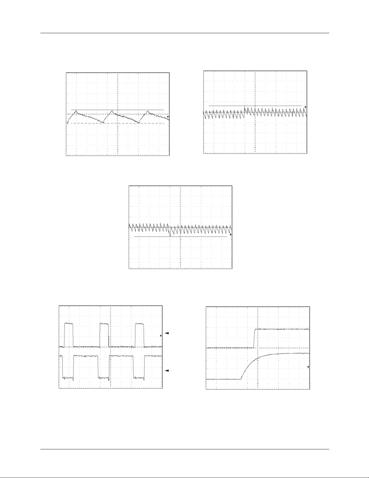
Typical Operating Characteristics
Output Ripple, 900m @ 3A
(20mV/div)
OUT
V
Time (1µs/division)
Transient Response, 0.1A to 3A
(continued)
(20mV/div)
OUT
V
Transient Response, 3A to 0.1A
Time (10µs/division)
Switching Waveforms, 3A Load Output Startup, System Power-up
2V/div 5V/div
(20mV/div)
OUT
V
Time (1µs/division)
Time (1µs/division)
HIDRV
pin
LODRV
pin
(500mV/div)
OUT
(2V/div ) V
IN
V
Time (5ms/division)
65-5051-12
6
REV. 2.1.4 11/13/01

PRODUCT SPECIFICATION FAN5066
Application Circuit
+12V
R6
324Ω
R7
909Ω
VID4
VID3
VID2
VID1
2.2
L1
H
µ
330µF
C9
0.1µF
C
C2
IN
12
13
14
15
16
19
17
18
20
C3
0.1µF
F
0.1µ
U1
FAN5066
C
100pF
ENABLE
EXT
1011
9
8
7
6
5
4
3
2
1
C7
0.1µF
R1
47Ω
D1
1N4735A
C5
F
1µ
C4
F
1µ
R4
C8
4.7Ω
4.7Ω
10KΩ
0.1µF
R2
R3
VCC
PWRGD
Q1
Q2
C6
0.1
µF
FDS6984S
4.7µ
R
L2
SENSE
H
25mΩ
C
OUT
470µF
VO
+5V
+5V
C1
R5
2KΩ
U2
FAN4041
0.1µF
Figure 1. Application Circuit for 900mV @ 3A
REV. 2.1.4 11/13/01
7

µ
FAN5066 PRODUCT SPECIFICATION
Table 2. FAN5066 Application Bill of Materials for 900mV @ 3A
Reference Manufacturer Part # Quantity Description Requirements/Comments
C1–3, C6–C9 Panasonic
ECU-V1H104ZFX
C4–5 Panasonic
ECU-V1C105ZFX
C
ext
Panasonic
ECU-V1H101JCG
C
IN
AVX
TPSE337*010R0100
C
OUT
AVX
TPSE477*006R0100
D1 Motorola
1N4735A
L1 Coiltronics
MP2-2R2
L2 Coiltronics
UP2B-4R7
Q1 Fairchild
FDS6984S
R1 Any 1 47 Ω
R2-3 Any 2 4.7 Ω
R4 Any 1 10K Ω
R5 Any 1 2.0K Ω
R6 Any 1 324 Ω
R7 Any 1 909Ω
R
SENSE
Any 1 25mΩ
U1 Fairchild
FAN5066M
U2 Fairchild
FAN4041
7 100nF, 50V Capacitor
21
F, 16V Capacitor
1 100pF Capacitor 5%, C0G
1 330 µ F, 10V Tantalum I
1 470 µ F, 6.3V Tantalum ESR
rms
= 1.3A
= 100m Ω
1 6.2V Zener Diode
1 2.2 µ H, 1.4A Inductor DCR ~ 130m Ω
See Note 1.
1 4.7 µ H, 5A inductor DCR ~ 17m Ω
1 N-Channel MOSFET with
Integrated Schottky
1 DC/DC Controller
1 Shunt Regulator
Notes:
1. Inductor L1 is recommended to isolate the 5V input supply from noise generated by the MOSFET switching. L1 may be
omitted if desired.
8
REV. 2.1.4 11/13/01

PRODUCT SPECIFICATION FAN5066
Application Circuit
+12V
+5V
C1
0.1µF
R5
499
R6
499
VDDQ
L1
1.5µ
H
C11
680µF
C2
12
13
14
15
16
17
18
19
20
C9
0.1µF
0.1µ
F
U1
FAN5066
C10
100pF
R1
47Ω
1011
9
8
7
6
5
4
3
2
1
D1
1N4735A
C5
F
1µ
C4
F
1µ
R2
4.7Ω
R3
4.7Ω
Q1
Q2
C6
0.1µF
1.5µ
L2
H
C
OUT
VO
*
ENABLE
C7
0.1µF
R4
C8
10KΩ
0.1µF
VCC
PWRGD
Figure 2. 12A Application Circuit for DDR VTT
*Refer to Table 3 for value
of C
OUT
.
REV. 2.1.4 11/13/01 9

FAN5066 PRODUCT SPECIFICATION
Table 3. FAN5066 Application Bill of Materials for DDR VTT
Reference Manufacturer Part # Quantity Description Requirements/Comments
C1–2, C6–C9 Panasonic
ECU-V1H104ZFX
C4–5 Panasonic
ECU-V1C105ZFX
C10 Panasonic
ECU-V1H101JCG
C11 Sanyo
6SP680M
C
OUT
Sanyo
4SP820M
D1 Motorola
1N4735A
L1 Coiltronics
UP1B-1R5
L2 Coiltronics
UP4B-1R5
Q1–2 Fairchild
FDS6680S
R1 Any 1 47Ω
R2-3 Any 2 4.7Ω
R4 Any 1 10KΩ
R5-6 Any 2 499Ω
U1 Fairchild
FAN5066M
6 100nF, 50V Capacitor
21µF, 16V Capacitor
1 100pF Capacitor 5%, C0G
1 680µF, 6.3V OSCON I
RMS
= 4.8A
4 820µF, 4V OSCON ESR < 12mΩ
1 6.2V Zener Diode
Optional 1.5µH, 4A Inductor DCR ~ 20mΩ
See Note 1.
1 1.5µH, 13A Inductor DCR ~ 4mΩ
2 N-Channel MOSFET
w/ Integrated Schottky
R
DS(ON)
V
GS
= 17mΩ @
= 4.5V
1 DC/DC Controller
Notes:
1. Inductor L1 is recommended to isolate the 5V input supply from noise generated by the MOSFET switching. L1 may be
omitted if desired.
Test Circuit
+12V
+5V
0.1µF
1µF
47Ω
VCCQP
VCCA
VCCP
GNDA GNDD GNDP
HIDRV
LODRV
1µF
4.7Ω
4.7Ω
3000pF
3000pF
t
R
90% 90%
50%
10% 10%
t
DT1
50% 50%
50%
t
F
t
DT2
HIDRV
LODRV
Figure 3. Output Drive Test Circuit and Timing Diagram
10 REV. 2.1.4 11/13/01

PRODUCT SPECIFICATION FAN5066
Application Information
The FAN5066 Controller
The FAN5066 is a programmable synchronous DC-DC controller IC. When designed around the appropriate external
components, the FAN5066 can be configured to deliver more
than 19A of output current. The FAN5066 functions as a
fixed frequency PWM step down regulator.
Main Control Loop
Refer to the FAN5066 Block Diagram on page 1. The
FAN5066 implements “summing mode control”, which is
different from both classical voltage-mode and current-mode
control. It provides superior performance to either by allowing a large converter bandwidth over a wide range of output
loads.
The control loop of the regulator contains two main sections:
the analog control block and the digital control block. The
analog section consists of signal conditioning amplifiers
feeding into a set of comparators which provide the inputs to
the digital control block. The signal conditioning section
accepts inputs from the IFB (current feedback) and VFB
(voltage feedback) pins and sets up two controlling signal
paths. The first, the voltage control path, amplifies the difference between the VFB signal the reference voltage from the
DAC and presents the output to one of the summing amplifier inputs. The second, current control path, takes the difference between the IFB and VFB pins and presents the
resulting signal to another input of the summing amplifier.
These two signals are then summed together with the slope
compensation input from the oscillator. This output is then
presented to a comparator, which provides the main PWM
control signal to the digital control block.
The digital control block takes the analog comparator inputs
and the main clock signal from the oscillator to provide the
appropriate pulses to the HIDRV and LODRV output pins.
These two outputs control the external power MOSFETs.
The digital block utilizes high speed Schottky transistor
logic, allowing the FAN5066 to operate at clock speeds as
high as 1MHz.
There are additional comparators in the analog control section whose function is to set the point at which the FAN5066
enters its pulse skipping mode during light loads, as well as
the point at which the current limit comparator disables the
output drive signals to the external power MOSFETs.
High Current Output Drivers
The FAN5066 contains two identical high current output
drivers that utilize high speed bipolar transistors in a pushpull configuration. The drivers’ power and ground are separated from the chip’s power and ground for switching noise
immunity. The HIDRV driver has a power supply pin,
VCCQP, which is supplied from an external 12V source
through a series resistor or from a charge-pump circuit
powered from 5V if 12V is not available. The LODRV driver
has a power supply pin, VCCP, which can be supplied from
either the 12V or 5V source. The resulting voltages are sufficient to provide the gate to source drive to the external
MOSFETs required in order to achieve a low R
DS,ON
.
Power Good (PWRGD)
The FAN5066 Power Good function is designed in accordance with the Pentium II DC-DC converter specifications
and provides a continuous voltage monitor on the VFB pin.
The circuit compares the VFB signal to the VREF voltage
and outputs an active-low interrupt signal to the CPU should
the power supply voltage deviate more than ±12% of its
nominal setpoint. The Power Good flag provides no other
control function to the FAN5066.
Output Enable (ENABLE)
The FAN5066 will accept an open collector/TTL signal for
controlling the output voltage. The low state disables the output voltage. When disabled, the PWRGD output is in the low
state. If an enable is not required in the circuit, this pin may
be left open.
Over-Voltage Protection
The FAN5066 constantly monitors the output voltage for
protection against over voltage conditions. If the voltage at
the VFB pin exceeds 20% of the selected program voltage,
an over-voltage condition is assumed and the FAN5066 disables the output drive signal to the external MOSFETs. The
DC-DC converter returns to normal operation after the fault
has been removed.
Over-Current Protection
Current sense is implemented in the FAN5066 to reduce the
duty cycle of the output drive signal to the MOSFETs when
an over-current condition is detected. The voltage drop
created by the output current flowing across a sense resistor
is presented to an internal comparator. When the voltage
developed across the sense resistor exceeds the 120mV comparator threshold voltage, the FAN5066 reduces the output
duty cycle to help protect the power devices. The DC-DC
converter returns to normal operation after the fault has been
removed.
Oscillator
The FAN5066 oscillator section uses a fixed current capacitor charging configuration. An external capacitor (CEXT) is
used to set the oscillator frequency between 80KHz and
1MHz. This scheme allows maximum flexibility in choosing
external components.
REV. 2.1.4 11/13/01 11

FAN5066 PRODUCT SPECIFICATION
In general, a higher operating frequency decreases the peak
ripple current flowing in the output inductor, thus allowing
the use of a smaller inductor value. In addition, operation at
higher frequencies decreases the amount of energy storage
that must be provided by the bulk output capacitors during
load transients due to faster loop response of the controller.
Unfortunately, the efficiency losses due to switching of the
MOSFETs increase as the operating frequency is increased.
Thus, efficiency is optimized at lower frequencies. An operating frequency of 300KHz is a typical choice which optimizes efficiency and minimizes component size while
maintaining excellent regulation and transient performance
under all operating conditions.
Design Considerations and Component
Selection
Additional information on design and component selection
may be found in Fairchild Semiconductor’s Application
Note 53.
MOSFET Selection
This application requires N-channel Logic Level Enhancement Mode Field Effect Transistors. Desired characteristics
are as follows:
• Low Static Drain-Source On-Resistance,
R
< 20mΩ (lower is better)
DS,ON
• Low gate drive voltage, VGS = 4.5V rated
• Power package with low Thermal Resistance
• Drain-Source voltage rating > 15V.
The on-resistance (R
) is the primary parameter for
DS,ON
MOSFET selection. The on-resistance determines the power
dissipation within the MOSFET and therefore significantly
affects the efficiency of the DC-DC Converter. For details
and a spreadsheet on MOSFET selection, refer to Applications Bulletin AB-8
MOSFET Gate Bias
The high side MOSFET gate driver can be biased by one of
two methods–Charge Pump or 12V Gate Bias. The charge
pump method has the advantage of requiring only +5V as an
input voltage to the converter, but the 12V method will realize increased efficiency by providing an increased VGS to the
high side MOSFETs.
Method 1. Charge Pump (Bootstrap)
Figure 4 shows the use of a charge pump to provide gate bias
to the high side MOSFET when +12V is unavailable. Capacitor CP is the charge pump used to boost the voltage of the
FAN5066 output driver. When the MOSFET Q1 switches
off, the source of the MOSFET is at approximately 0V
because of the MOSFET Q2. (The Schottky D2 conducts for
only a very short time, and is not relevent to this discussion.)
CP is charged through the Schottky diode D1 to approxi-
mately 4.5V. When the MOSFET Q1 turns on, the voltage at
the source of the MOSFET is equal to 5V. The capacitor
voltage follows, and hence provides a voltage at VCCQP
equal to almost 10V. The Schottky diode D1 is required to
provide the charge path when the MOSFET is off, and
reverses biases when VCCQP goes to 10V. The charge pump
capacitor (CP) needs to be a high Q, high frequency capacitor. A 1µF ceramic capacitor is recommended here.
+5V
CP
D1
Q1
L2 RS
Q2
D2
VO
C
OUT
VCCQP
HIDRV
PWM/PFM
Control
LODRV
GNDP
Figure 4. Charge Pump Configuration
Method 2. 12V Gate Bias
Figure 5 illustrates how a 12V source can be used to bias
VCCQP. A 47Ω resistor is used to limit the transient current
into the VCCQP pin and a 1µF capacitor is used to filter the
VCCQP supply. This method provides a higher gate bias
voltage (VGS) to the high side MOSFET than the charge
pump method, and therefore reduces the R
DS,ON
and the
resulting power loss within the MOSFET. In designs where
efficiency is a primary concern, the 12V gate bias method is
recommended. A 6.2V Zener diode, D1, is used to clamp the
voltage at VCCQP to a maximum of 12V and ensure that the
absolute maximum voltage of the IC will not be exceeded.
+5V
+12V
VCCQP
PWM/PFM
Control
LODRV
GNDP
Figure 5. Gate Bias Configuration
HIDRV
47Ω
1µF
D1
Q1
L2 RS
Q2
D2
VO
C
OUT
12 REV. 2.1.4 11/13/01

PRODUCT SPECIFICATION FAN5066
Inductor Selection
Choosing the value of the inductor is a tradeoff between
allowable ripple voltage and required transient response. The
system designer can choose any value within the allowed
minimum to maximum range in order to either minimize ripple or maximize transient performance. The first order equation (close approximation) for minimum inductance is:
VinV
–()
min
------------------------------
f
L
out
V
out
-----------
V
in
-----------------
××=
V
ESR
ripple
where:
Vin = Input Power Supply
V
= Output Voltage
out
f = DC/DC converter switching frequency
ESR = Equivalent series resistance of all output capacitors in
parallel
V
= Maximum peak to peak output ripple voltage
ripple
budget.
The first order equation for maximum allowed inductance is:
L
max
------------------------------------------------
×=
2C
O
I
out
2
PP
tb
VinV
–()DmV
where:
Co = The total output capacitance
Ipp = Maximum to minimum load transient current
Vtb = The output voltage tolerance budget allocated to load
transient
Dm = Maximum duty cycle for the DC/DC converter
(usually 95%).
Some margin should be maintained away from both L
and L
. Adding margin by increasing L almost always
max
min
adds expense since all the variables are predetermined by
system performance except for Co, which must be increased
to increase L. Adding margin by decreasing L can either be
done by purchasing capacitors with lower ESR or by increasing the DC/DC converter switching frequency. The
FAN5066 is capable of running at high switching frequencies and provides significant cost savings for the newer CPU
systems that typically run at high supply current.
FAN5066 Short Circuit Current Characteristics
The FAN5066 short circuit current characteristic includes a
hysteresis function that prevents the DC-DC converter from
oscillating in the event of a short circuit. Figure 6 shows the
typical characteristic of the DC-DC converter circuit with a
6.8 mΩ sense resistor. The converter exhibits a normal load
regulation characteristic until the voltage across the resistor
exceeds the internal short circuit threshold of 120mV
(= 17.5A * 6.8mΩ). At this point, the internal comparator
trips and signals the controller to reduce the converter’s
duty cycle to approximately 20%. This causes a drastic
reduction in the output voltage as the load regulation
collapses into the short circuit control mode. With a 40mΩ
output short,the voltage is reduced to 15A * 40mΩ = 600mV.
Output Voltage vs. Output Current
3.5
3.0
2.5
2.0
1.5
OUT (V)
1.0
0.5
0
0 5 10 15 20 25
Figure 6. FAN5066 Short Circuit Characteristic
RSENSE = 6m
Output Current (A)
Ω
The output voltage does not return to its nominal value until
the output current is reduced to a value within the safe operating range for the DC-DC converter
Schottky Selection
A schottky diode is not required in Figures 1 and 2, because
the low-side MOSFETs have built in schottkies using Fairchild SyncFET technology. If some other type of MOSFET
is used, a schottky must be used in anti-parallel with the lowside MOSFET. Selection of a schottky is determined by the
maximum output. In the converter of Figure 1, maximum
output current is 3A, and suppose the MOSFET has a body
diode V
least 100mV less V
= 0.75V at this current. The schottky must have at
f
at the same current to ensure that the
f
body diode does not turn on. The MBRS130L diode has Vf =
0.45V typical at 3A at 25°C, and so is a suitable choice.
Output Filter Capacitors
The output bulk capacitors of a converter help determine its
output ripple voltage and its transient response. It has
already been seen in the section on selecting an inductor that
the ESR helps set the minimum inductance, and the capacitance value helps set the maximum inductance. For most
converters, however, the number of capacitors required is
determined by the transient response and the output ripple
voltage, and these are determined by the ESR and not the
capacitance value. That is, in order to achieve the necessary
ESR to meet the transient and ripple requirements, the
capacitance value required is already very large.
The most commonly used choice for output bulk capacitors
is aluminum electrolytics, because of their low cost and low
ESR. The only type of aluminum capacitor used should be
those that have an ESR rated at 100kHz. Consult Application
Bulletin AB-14 for detailed information on output capacitor
selection.
The output capacitance should also include a number of
small value ceramic capacitors placed as close as possible to
the processor; 0.1µF and 0.01µF are recommended values.
REV. 2.1.4 11/13/01 13

FAN5066 PRODUCT SPECIFICATION
Input Filter
The DC-DC converter design may include an input inductor
between the system +5V supply and the converter input as
shown in Figure 6. This inductor serves to isolate the +5V
supply from the noise in the switching portion of the DC-DC
converter, and to limit the inrush current into the input capacitors during power up. A value of 2.5µH is recommended.
It is necessary to have some low ESR aluminum electrolytic
capacitors at the input to the converter. These capacitors
deliver current when the high side MOSFET switches on.
Figure 7 shows 3 x 1000µF, but the exact number required
will vary with the speed and type of the processor. For the
top speed Klamath and Deschutes, the capacitors should be
rated to take 7A of ripple current. Capacitor ripple current
rating is a function of temperature, and so the manufacturer
should be contacted to find out the ripple current rating at the
expected operational temperature. For details on the design
of an input filter, refer to Applications Bulletin AB-15.
5V
0.1µF
2.5µH
Vin
1000µF, 10V
Electrolytic
Figure 7. Input Filter
Droop Resistor
Figure 8 shows a converter using a “droop resistor”, RD. The
function of the droop resistor is to improve the transient
response of the converter, potentially reducing the number of
output capacitors required. In operation, the droop resistor
causes the output voltage to be slightly lower at heavy load
current than it otherwise would be. When the load transitions
from heavy to light current, the output can swing up farther
without exceeding limits, because it started from a lower
voltage, thus reducing the capacitor requirements.
Q1
L2
Q2
Figure 8. Use of a Droop Resistor
R
SENSERDROOP
IFB VFB
VO
C
OUT
PCB Layout Guidelines
• Placement of the MOSFETs relative to the FAN5066 is
critical. Place the MOSFETs such that the trace length of
the HIDRV and LODRV pins of the FAN5066 to the FET
gates is minimized. A long lead length on these pins will
cause high amounts of ringing due to the inductance of the
trace and the gate capacitance of the FET. This noise
radiates throughout the board, and, because it is switching
at such a high voltage and frequency, it is very difficult to
suppress.
• In general, all of the noisy switching lines should be kept
away from the quiet analog section of the FAN5066. That
is, traces that connect to pins 9, 12, and 13 (LODRV,
HIDRV and VCCQP) should be kept far away from the
traces that connect to pins 1 through 5, and pin 16.
• Place the 0.1µF decoupling capacitors as close to the
FAN5066 pins as possible. Extra lead length on these
reduces their ability to suppress noise.
• Each VCC and GND pin should have its own via to the
appropriate plane. This helps provide isolation between
pins.
• Surround the CEXT timing capacitor with a ground trace.
Be sure to place a ground or power plane underneath the
capacitor for further noise isolation, in order to provide
additional shielding to the oscillator (pin 1) from the noise
on the PCB. In addition, place this capacitor as close to
pin 1 as possible.
• Place the MOSFETs, inductor, and Schottky as close
together as possible for the same reasons as in the first
bullet above. Place the input bulk capacitors as close to
the drains of the high side MOSFETs as possible. In
addition, placement of a 0.1µF decoupling cap right on
the drain of each high side MOSFET helps to suppress
some of the high frequency switching noise on the input
of the DC-DC converter.
• Place the output bulk capacitors as close to the CPU as
possible to optimize their ability to supply instantaneous
current to the load in the event of a current transient.
Additional space between the output capacitors and the
CPU will allow the parasitic resistance of the board traces
to degrade the DC-DC converter’s performance under
severe load transient conditions, causing higher voltage
deviation. For more detailed information regarding
capacitor placement, refer to Application Bulletin AB-5.
• The traces that run from the FAN5066 IFB (pin 4) and
VFB (pin 5) pins should be run together next to each other
and Kelvin connected to the sense resistor. Running these
lines together rejects some of the common mode noise
that is presented to the FAN5066 feedback input. Try, as
much as possible, to run the noisy switching signals
(HIDRV, LODRV & VCCQP) on one layer, but use the
inner layers for power and ground only. If the top layer is
being used to route all of the noisy switching signals, use
the bottom layer to route the analog sensing sign VFB and
IFB.
• A PC Board Layout Checklist is available from Fairchild
Applications. Ask for Application Bulletin AB-11.
14 REV. 2.1.4 11/13/01

PRODUCT SPECIFICATION FAN5066
Additional Information
For additional information contact your local Fairchild
Semiconductor representative, or visit us on our website at
www.fairchildsemi.com.
REV. 2.1.4 11/13/01 15

FAN5066 PRODUCT SPECIFICATION
Mechanical Dimensions – 20 Lead SOIC
Symbol
A .093 .104 2.35 2.65
A1 .004 .012 0.10 0.30
B .013 0.33
C .009 .013 0.23 0.32
D .496 .512 12.60 13.00
E .291 .299 7.40 7.60
e
H
h
L .016 .050 0.40 1.27
N20 20
α
ccc .004 0.10——
20
Inches
Min. Max. Min. Max.
.020 0.51
.050 BSC 1.27 BSC
.394 .419 10.00 10.65
.010 .029 0.25 0.75
0° 8° 0° 8°
Millimeters
11
EH
Notes
5
2
2
3
6
Notes:
1.
Dimensioning and tolerancing per ANSI Y14.5M-1982.
2.
"D" and "E" do not include mold flash. Mold flash or
protrusions shall not exceed .010 inch (0.25mm).
3.
"L" is the length of terminal for soldering to a substrate.
4.
Terminal numbers are shown for reference only.
5.
"C" dimension does not include solder finish thickness.
6.
Symbol "N" is the maximum number of terminals.
1
D
A
e
B
10
A1
SEATING
PLANE
– C –
LEAD COPLANARITY
ccc C
h x 45°
C
α
L
16 REV. 2.1.4 11/13/01

PRODUCT SPECIFICATION FAN5066
Mechanical Dimensions – 20 Lead TSSOP
Symbol
A — .047 — 1.20
A1 .002 .006 0.05 0.15
B .007 0.19
C .004 .008 0.09 0.20
D .252 .260 6.40 6.60
E .169 .177 4.30 4.50
e
H
L
N20 20
α
ccc .004 0.10——
Inches
Min. Max. Min. Max.
.012 0.30
.026 BSC 0.65 BSC
.252 BSC 6.40 BSC
.018 .030 0.45 0.75
0° 8° 0° 8°
D
Millimeters
E
H
Notes
2
2
3
5
Notes:
1.
Dimensioning and tolerancing per ANSI Y14.5M-1982.
2.
"D" and "E" do not include mold flash. Mold flash or
protrusions shall not exceed .006 inch (0.15mm).
3.
"L" is the length of terminal for soldering to a substrate.
4.
Terminal numbers are shown for reference only.
5.
Symbol "N" is the maximum number of terminals.
A
e
A1
B
SEATING
PLANE
– C –
LEAD COPLANARITY
ccc C
α
L
C
REV. 2.1.4 11/13/01 17

FAN5066 PRODUCT SPECIFICATION
Ordering Information
Product Number Package
FAN5066M 20 pin SOIC
FAN5066MTC 20 pin TSSOP
FAN5066MTCX 20 pin TSSOP
DISCLAIMER
FAIRCHILD SEMICONDUCTOR RESERVES THE RIGHT TO MAKE CHANGES WITHOUT FURTHER NOTICE TO ANY
PRODUCTS HEREIN TO IMPROVE RELIABILITY, FUNCTION OR DESIGN. FAIRCHILD DOES NOT ASSUME ANY
LIABILITY ARISING OUT OF THE APPLICATION OR USE OF ANY PRODUCT OR CIRCUIT DESCRIBED HEREIN; NEITHER
DOES IT CONVEY ANY LICENSE UNDER ITS PATENT RIGHTS, NOR THE RIGHTS OF OTHERS.
LIFE SUPPORT POLICY
FAIRCHILD’S PRODUCTS ARE NOT AUTHORIZED FOR USE AS CRITICAL COMPONENTS IN LIFE SUPPORT DEVICES
OR SYSTEMS WITHOUT THE EXPRESS WRITTEN APPROVAL OF THE PRESIDENT OF FAIRCHILD SEMICONDUCTOR
CORPORATION. As used herein:
1. Life support devices or systems are devices or systems
which, (a) are intended for surgical implant into the body,
or (b) support or sustain life, or (c) whose failure to perform
when properly used in accordance with instructions for use
2. A critical component is any component of a life support
device or system whose failure to perform can be
reasonably expected to cause the failure of the life support
device or system, or to affect its safety or effectiveness.
provided in the labeling, can be reasonably expected to
result in significant injury to the user.
www.fairchildsemi.com
11/13/01 0.0m 001
2001 Fairchild Semiconductor Corporation
Stock#DS30005066
 Loading...