

www.fairchildsemi.com
FAN5037
Adjustable Switching Regulator Controller
Features
• High power switch-mode DC-DC controller can provide
in excess of 13A
• Output voltage adjustable from 1.2V to 3.6V
• 85% efficiency
• Cumulative accuracy < 3% over line, load, and
temperature variations
• Overvoltage and short circuit protection
• Built-in soft start
• No overshoot at turn-on
Applications
• I/O and AGP power for desktop computers
• High efficiency power for ASICs
• High efficiency power for DSPs
• Adjustable step-down power supplies
Description
The F AN5037 is a high power, switch-mode DC-DC controller that provides efficient power for all low-voltage applications. This controller has a built-in Soft Start feature which
offers system protection during power-up by reducing both
inrush current and output overshoot. When combined with
the appropriate external circuitry, the FAN5037 can deliver
load currents as high as 13A at efficiencies as high as 88%.
The FAN5037 can generate output voltages from 1.2V up to
3.6V using external resistors.
The FAN5037 is designed to operate in a constant on-time
control mode under all load conditions. Its accurate low TC
reference eliminates the need for precision external components in order to achieve the tight tolerance voltage regulation required by many applications. Short circuit current
protection is provided through the use of a current sense
resistor, while overvoltage protection is provided internally.
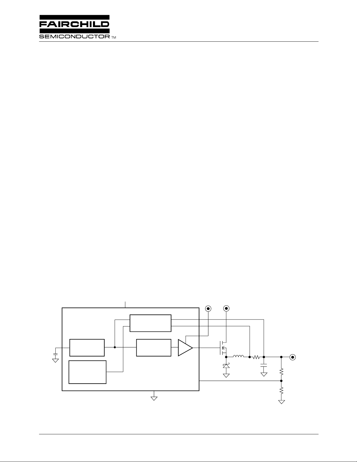
Block Diagram
FAN5037
CEXT
1
Oscillator
1.20V
Reference
VCCA 2
Feedback Control
Digital Logic
GNDP 6
+12V5V+5V
IFBL 4
IFBH 3
VCCP 8
7
DRV
Vout
VFB 5
REV. 1.0.3 9/26/01
.
.
FAN5037 PRODUCT SPECIFICATION
Pin Assignments
Pin Descriptions
Pin
Name
CEXT 1
VCCA 2
IFBH 3
IFBL 4
VFB 5
GNDP 6
DRV 7
VCCP 8
Pin
Number Pin Function Description
External capacitor. A 180pF capacitor is connected to this pin as part of the constant
on-time pulse width circuit. Careful layout of this pin is critical to system performance.
See Applications Information for details.
Analog V
system 5V supply and decouple to ground with 0.1µF ceramic capacitor.
High side current feedback. Pins 3 and 4 are used as the inputs for the current feedback
control loop and as the short circuit current sense points. Careful layout of the traces from
these pins to the current sense resistor is critical for optimal performance of the short circuit
protection scheme. See Applications Information for details.
Low side current feedback. See Applications Information for details.
Voltage feedback. Using two external resistors, this pin sets the output voltage level for the
switching regulator.
Power Ground. Connect to a low impedance ground. See Application Information for
details.
MOSFET driver output. Connect this pin to the gate of the N-channel MOSFET Q1 as
shown in Figure 12. The trace from this pin to the MOSFET gate should be kept as short as
possible (less than 0.5"). See Applications Information for details.
Power V
filter shown in Figure 12. See Applications Information for details.
CEXT
VCCA
IFBH
IFBL VFB
Power supply for regulator control circuitry and voltage reference. Connect to
cc
Power supply for DRV output driver. Connect to system 12V supply with R-C
cc
1
2
3
45
FAN5037
VCCP
8
DRV
7
GNDP
6
Absolute Maximum Ratings
Supply V oltages, VCCA 7V
Supply V oltages, VCCP 13V
Junction Temperature, T
Storage Temperature, T
J
S
+150°C
-65 to +150°C
Lead Soldering Temperature, 10 seconds 300°C
Thermal Resistance Junction-to-Ambient, Θ
Note:
1. Functional operation under any of these conditions is not implied. Performance is guaranteed only if Operating Conditions
are not exceeded.
JA
163°C/W
Operating Conditions
Parameter Conditions Min. Typ. Max. Units
Switching Regulator Supply, VCCA 4.75 5 5.25 V
Ambient Operating Temperature, T
A
Gate Drive Supply, VCCP 9.5 12 12.6 V
2
070°C
REV. 1.0.3 9/26/01
•
•
•
•
•
•
PRODUCT SPECIFICATION FAN5037
Electrical Characteristics
(VCCA = 5V, VCCP = 12V, T
The • denotes specifications which apply over the full ambient operating temperature range.
Parameter Conditions Min. Typ. Max. Units
Output Voltage 1.2 3.6 V
Output Temperature Drift T
Line Regulation VCCA = 4.75 to 5.25V, I
Load Regulation I
V
PSRR VCCA = 4.75 to 5.25V 60 dB
OUT
Output Ripple, peak-peak 20MHz BW, I
Total DC Accuracy
1
Efficiency I
Output Driver Current Open Loop
Short Circuit Threshold Voltage
Undervoltage Lockout
On Time Pulse Width
VCCA Supply Current Independent of load
VCCP Supply Current I
= 25
°
A
C using circuit of Figure 1, unless otherwise noted)
= 0˚C–70˚C 40 ppm/˚C
A
= 13A 3 5 mV
LOAD
= 0 to 5A or 5A to 13A 30 43 mV
LOAD
= 13A 15 mV
LOAD
±55 ±100 mV
= 5A 80 85 %
LOAD
0.5 A
70 90 100 mV
3.5 4.0 4.5 V
2
C
= 180pF 3.5 µs
EXT
515mA
LOAD
= 13A
20 25 mA
Notes:
1. Total DC accuracy includes setpoint accuracy, temperature drift, line and load regulation.
2. The on-time pulse width of the oscillator is set via external capacitor C
EXT
.
REV. 1.0.3 9/26/01
3
FAN5037 PRODUCT SPECIFICATION
Typical Operating Characteristics
(VCCA = 5V, and T
= +25
A
°
C using circuit in Figure 1, unless otherwise noted)
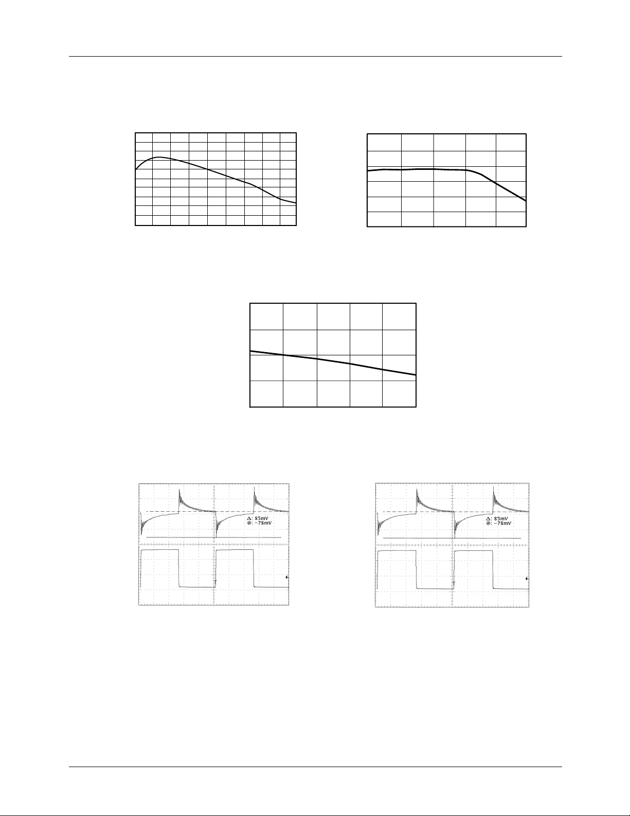
95
94
93
92
91
90
89
88
Efficiency (%)
87
86
85
12 3 4 5
Efficiency vs. Output Current
678910
Output Current
Output Voltage vs. Temperature, I
+0.50
+0.25
Nom.
-0.25
Output Voltage (%)
-0.50
025
+1.5
+1.0
+0.5
(%)
Nom
OUT
V
50 75
Output Voltage vs. Load
-0.5
-1.0
-1.5
02468
Output Current (A)
= 10A
OUT
100 125
10
Transient Response, 0.5 to 5.5A
(50mV/div)
OUT
(2A/div) V
SW
I
Time (100µs/division)
Output Ripple, I
(10mV/division)
OUT
V
= 10A)
OUT
Time (2µs/division)
4
REV. 1.0.3 9/26/01

PRODUCT SPECIFICATION FAN5037
Typical Operating Characteristics
Output Startup, System Power-Up
Time (5ms/division)
Pin 7 (DRV), 0.1A Load
(continued)
Pin 7 (DRV), 10A Load
Time (1µs/division)
Application Circuit
Optional
+5V
+12V
0.1µF
C1
0.1uF
C7
2.5µH
C6
180pF
L1
R1
47Ω
C5
Time (1µs/division)
R2
C4
+
1200µF
Q1
4.7Ω
FDB6030L
D1
MBRB1545CT
D2
MMBD4148
D3
1N4735A
1µF
1200µF
1
2
3
FAN5037
4
C2
+
U1
C3
+
1200µF
8
7
6
5
Figure 1. 13A at 3.3V Application Schematic
C8
L2
4.7µH
0.1µF
R3
5.2mΩ
R4
3.48KΩ
R5
2KΩ
+ +
...
V
CORE
C14
1500µF
REV. 1.0.3 9/26/01
5

FAN5037 PRODUCT SPECIFICATION
Table1. Bill of Materials for a FAN5037 3.3V, 13A Application
Manufacturer
Qty. Reference
3 C1, C7-8 Any 100nF, 25V Capacitor
3 C2-4 Sanyo
1
C5
1
C6
6 C9-14 Sanyo
1 R1 Any 47.5 Ω
1 R2 Any 4.75 Ω
1 R3 N/A 5.2m Ω , 1W Resistor PCB Trace Resistor, see
1 R4 Any 3.48K Ω
1 R5 Any 2K Ω
1 D1 Motorola
1 D2 Fairchild
1 D3 Motorola
1 Q1 Fairchild
Optional L1 Any 2.5µH Inductor I
1 L2 Any 4.7µH Inductor I
1 U1 Fairchild
Part Order # Description
1200µF, 10V Aluminum Capacitor I
10MV1200GX
Any 1µF, 25V Capacitor
Any 180pF, 50V Capacitor C0G
1500µF, 6.3V Aluminum Capacitor ESR = 44m Ω
6MV1500GX
15A, 45V Schottky
MBRB1545CT
Signal Diode
MMBD4148
6.2V Zener
1N4735A
30V, 14m Ω Logic Level MOSFET
FDB6030L
PWM Controller
FAN5037M
Requirements
and Comments
= 2A , See Equation
RMS
(2) in Applications
Equation (3) Applications
> 8A
SAT
> 13A
SAT
Application Information
The FAN5037 contains a precision trimmed zero TC voltage
reference, a constant-on-time architecture controller, a high
current output driver, and a low offset error amp. The
detailed block diagram in Figure 1 shows how the FAN5037
works together with external components to achieve a highperformance switching power supply.
Switch-Mode Control Loop
The main control loop for the switch-mode converter consists
of a current conditioning amplifier and a voltage conditioning
amplifier. The voltage amplifier compares the voltage from the
internal reference with the converter’s output voltage divided
by an external resistor divider. The current amplifier senses the
current by comparing the voltages at the IFBH and IFBL pins,
which are attached to either side of the current sense resistor.
The signals from the voltage and current amplifiers are
summed together, the result being used to control the off-time
of the oscillator. The current feedback signal is also used as
part of the F AN5037 short-circuit protection.
6
High Current Output Drivers
The FAN5037 high current output driver (DRV) contains
high speed bipolar power transistors configured in a
push-pull configuration. The output driver is capable of supplying 0.5A of current in less than 100ns. The driver’s power
and ground are separated from the overall chip power and
ground for added switching noise immunity.
Internal Reference
The reference in the FAN5037 is a precision band-gap type
reference. Its temperature coefficient is trimmed to provide a
near zero TC.
Constant-On-Time Oscillator
The FAN5037 switch-mode oscillator is designed as a fixed
on-time, variable off-time oscillator. The constant-on-time
oscillator consists of a comparator, an external capacitor, a
fixed current source, a variable current source, and an analog
switch that selects between two threshold voltages for the
comparator. The external timing capacitor is alternately
REV. 1.0.3 9/26/01

7
PRODUCT SPECIFICATION FAN5037
charged and discharged through the enabling and disabling
of the fixed current source. The variable current source is
controlled from the error inputs that are received from the
current and voltage feedback signals. The oscillator off-time
is controlled by the amount of current that is available from
g
m
Constant On-Time Oscillator
I
O
V
H
V
L
I
ON
6
GNDP
CEXT
g
m
1
REF
the variable current source to charge the external capacitor up
to the high threshold level of the comparator. The on-time is
set by the constant current source that discharges the external
capacitor voltage down to the lo wer comparator threshold.
+5V
+12V
VCCA
2
4
IFBL
IFBH
3
VCCP
8
SDRV
7
V
OUT
FBSW
5
65-5037-07
Figure 2. FAN5037 Detailed Block Diagram
Output V oltage Selection
The FAN5037 precision reference is trimmed to be 1.2V
nominally. When using the FAN5037, the system designer
has complete flexibility in choosing the output voltage for
one regulator from 1.2V to 3.6V. This is done by appropriately selecting the feedback resistors. These could be 0.1%
resistors to realize optimum output accuracy. The following
equations determines the output voltage of the regulator:
V
OUT
-------------------- -
1.2
×=
R5
(1)
R4 R5+
For example, for 3.3V:
V
OUT
R4 R5+
-------------------- -
1.2
× 1.2
R5
3.48k 2.0k+
------------------------------ -
× 3.3V== =
2.0k
Input Capacitors
The number of input capacitors required for the FAN5037 is
dependent on their ripple current rating, which assures their
rated life. The number required may be determined by
*
DC DC2–
I
out
No. Caps
where the duty cycle DC = (V
--------------------------------------- -=
I
rating
+
out
V
f,diode
)
ple, with a 1.5V output at 10A, 5V input, and using the
Sanyo capacitors specified in Table 1 which have a 2A ripple
current rating, we have DC = (1.5
+
.5)/5 = 0.4, and
/
V
. For exam-
in
(2)
No. Caps
*
10 0.4 0.4
---------------------------------- - 2.44==
2
–
2
so that we need 3 input capacitors.
Short Circuit Considerations
The FAN5037 uses a current sensing scheme to limit the load
current if an output fault condition occurs. The current sense
resistor carries the peak current of the inductor, which is
greater than the maximum load current due to ripple current
flowing in the inductor. The FAN5037 will begin to limit the
output current to the load by reducing the duty cycle of the
top-side MOSFET driver when the voltage across the current-sense resistor exceeds the short circuit comparator
threshold voltage (V
age will temporarily go out of regulation. As the voltage
across the sense resistor becomes larger, the duty cycle of the
top-side MOSFET will continue to be reduced until the current limit value is reached. At this point, the FAN5037 will
continuously deliver the limit current at a reduced output
voltage level. The short circuit comparator threshold voltage
is typically 90mV, with a tolerance of ±10mV. The ripple
current flowing through the inductor in Figure 1 is 0.6Apeak.
Refer to Application Note AB-23 for detailed discussions.
The sense resistor value can be approximated as follows:
V
th,min
R
SENSE
---------------I
PK
). When this happens the output volt-
th
V
th,min
1TF–()×
---------------------------------------------
0.6A I
+
LOAD,MAX
1TF–()×==
(3)
REV. 1.0.3 9/26/01

FAN5037 PRODUCT SPECIFICATION
where TF = Tolerance Factor for the sense resistor and 0.6A
accounts for the inductor ripple current.
Since the value of the sense resistor is often less than 10mΩ,
care should be taken in the layout of the PCB. Trace resistance can contribute significant errors. The traces to the
IFBH and IFBL pins of the FAN5037 should be Kelvin connected to the pads of the current-sense resistor. To minimize
the influence of noise, the two traces should be run next to
each other.
Schottky Diode
In Figure 1, MOSFET Q1 and flyback diode D1 are used as
complementary switches in order to maintain a constant current through the output inductor L2. As a result, D1 will have
to carry the full current of the output load when the power
MOSFET is turned off. The power in the diode is a direct
function of the forward voltage at the rated load current during the off time of the FET. The following equation can be
used to estimate the diode power:
P
DIODEIDVD
where ID is the forward current of the diode, VD is the forward voltage of the diode, and DutyCycle is defined the
same as
Duty Cycle
For the Motorola MBRB1545CT Rectifier in Figure 1,
P
DIODE
10A 0.65 1 73.1%–()×× 1.75W==
Vout
------------ -=
Vin
1 DutyCycle–()××=
Board Design Considerations
MOSFET Placement
Placement of the power MOSFET is critical in the design of
the switch-mode regulator . The MOSFET should be placed
in such a way as to minimize the length of the gate drive path
from the FAN5037 SDRV pin. This trace should be kept
under 0.5" for optimal performance. Excessive lead length
on this trace will cause high frequency noise resulting from
the parasitic inductance and capacitance of the trace. Since
this voltage can transition nearly 12V in around 100nsec, the
resultant ringing and noise would be very difficult to suppress. This trace should be routed on one layer only and kept
well away from the “quiet” analog pins of the device: CEXT,
IFBH, IFBL, and GND. Refer to Figure 2. A 4.7Ω resistor in
series with the MOSFET gate can decrease this layout criticality. Refer to Figure 1.
Inductor and Schottky Diode Placement
The inductor and fly-back Schottky diode need to be placed
close to the source of the power MOSFET for the same reasons stated above. The node connecting the inductor and
Schottky diode will swing between the drain voltage of the
FET and the forward voltage of the Schottky diode. It is recommended that this node be converted to a plane if possible.
This node will be part of the high current path in the design,
and as such it is best treated as a plane in order to minimize
the parasitic resistance and inductance on that node. Since
most PC board manufacturers utilize 1/2 oz copper on the
top and bottom signal layers of the PCB, it is not recommended to use these layers to route the high current portions
of the regulator design. Since it is more common to use 1 oz.
copper on the PCB inner layers, it is recommended to use
those layers to route the high current paths in the design.
It is recommended that the diode T0-220 package be
attached to a heatsink.
Example of
a Good Layout
5
6
7
Noisy signal is routed
away from quiet pins and the
trace length is kept under 0.5in.
The gate resistor is as close
as possible to the MOSFET.
Figure 3. Examples of good and poor layouts
8
4
3
2
1
a Problem Layout
= "Quiet" Pins
Example of
5
4
6
3
7
2
81
Noisy signal radiates
onto quiet pins and the
trace is too long.
Gate resistor is far away
from the MOSFET.
8 REV. 1.0.3 9/26/01

PRODUCT SPECIFICATION FAN5037
Power and Ground Connections
The connection of VCCA to the 5V power supply plane
should be short and bypassed with a 0.1µF directly at the
VCCA pin of the FAN5037. The ideal connection would be a
via down to the 5V power plane. A similar arrangement
should be made for the VCCP pin that connects to +12V.
Each ground should have a separate via connection to the
ground plane below.
A 12V power supply is used to bias the VCCP. A 47Ω resistor is used to limit the transient current into VCCP. A 1uF
capacitor filter is used to filter the VCCP supply and source
the transient current required to charge the MOSFET gate
capacitance. This method provides sufficiently high gate bias
voltage to the MOSFET (V
R
of the MOSFET and its power loss.
DS(ON)
), and therefore reduces
GS
Figure 4 provides about 5V of gate bias which works well
when using typical logic-level MOSFETs. Non-logic-level
MOSFETs should not be used because of their higher
R
DS(ON)
.
MOSFET Gate Bias
+5V
+12V
47Ω
VCCP
1µF
GNDP
Figure 4. 12V Gate Bias Configuration
Q1
D1
L2
R
SENSE
C
V
BULK
OUT
REV. 1.0.3 9/26/01 9

PRODUCT SPECIFICATION FAN5037
85
14
D
A
A1
– C –
ccc C
LEAD COPLANARITY
SEATING
PLANE
e
B
L
h x 45°
C
α
EH
A .053 .069 1.35 1.75
Symbol
Inches
Min. Max. Min. Max.
Millimeters
Notes
A1 .004 .010 0.10 0.25
.020 0.51
B .013 0.33
C .008 .010 0.20 0.25
E .150 .158 3.81 4.01
e
.228 .244 5.79 6.20
.010 .020 0.25 0.50
H
.050 BSC 1.27 BSC
h
L .016 .050 0.40 1.27
0° 8° 0° 8°
3
6
5
2
2
N8 8
α
ccc .004 0.10——
D .189 .197 4.80 5.00
Notes:
1.
2.
3.
4.
5.
6.
Dimensioning and tolerancing per ANSI Y14.5M-1982.
"D" and "E" do not include mold flash. Mold flash or
protrusions shall not exceed .010 inch (0.25mm).
"L" is the length of terminal for soldering to a substrate.
Terminal numbers are shown for reference only.
"C" dimension does not include solder finish thickness.
Symbol "N" is the maximum number of terminals.
Mechanical Dimensions
8 Lead SOIC Package
REV. 1.0.3 9/26/01 10

FAN5037 PRODUCT SPECIFICATION
Ordering Information
Product Number Package
FAN5037M 8 pin SOIC
DISCLAIMER
FAIRCHILD SEMICONDUCTOR RESERVES THE RIGHT TO MAKE CHANGES WITHOUT FURTHER NOTICE TO
ANY PRODUCTS HEREIN TO IMPROVE RELIABILITY, FUNCTION OR DESIGN. FAIRCHILD DOES NOT ASSUME
ANY LIABILITY ARISING OUT OF THE APPLICATION OR USE OF ANY PRODUCT OR CIRCUIT DESCRIBED HEREIN;
NEITHER DOES IT CONVEY ANY LICENSE UNDER ITS PATENT RIGHTS, NOR THE RIGHTS OF OTHERS.
LIFE SUPPORT POLICY
FAIRCHILD’S PRODUCTS ARE NOT AUTHORIZED FOR USE AS CRITICAL COMPONENTS IN LIFE SUPPORT DEVICES
OR SYSTEMS WITHOUT THE EXPRESS WRITTEN APPROVAL OF THE PRESIDENT OF FAIRCHILD SEMICONDUCTOR
CORPORATION. As used herein:
1. Life support devices or systems are devices or systems
which, (a) are intended for surgical implant into the body, or
(b) support or sustain life, and (c) whose failure to perform
when properly used in accordance with instructions for use
2. A critical component in any component of a life support
device or system whose failure to perform can be reasonably expected to cause the failure of the life support device
or system, or to affect its safety or effectiveness.
provided in the labeling, can be reasonably expected to
result in a significant injury of the user.
www.fairchildsemi.com
9/26/01 0.0m 001
2001 Fairchild Semiconductor Corporation
Stock#DS30005037
 Loading...