


FAN5026
FAN5026 — Dual DDR / Dual-Output PWM Controller
March 2011
Dual DDR / Dual-Output PWM Controller
Features
Highly Flexible, Dual Synchronous Switching PWM
Controller that Includes Modes for:
-
DDR Mode with In-phase Operation for
Reduced Channel Interference
-
90° Phase-shifted, Two-stage DDR Mode
for Reduced Input Ripple
-
Dual Independent Regulators, 180° Phase
Shifted
Complete DDR Memory Power Solution
-
V
Tracks V
TT
-
V
Buffered Reference Output
DDQ/2
Lossless Current Sensing on Low-Side MOSFET or
Precision Over-Current Using Sense Resistor
VCC Under-Voltage Lockout
Wide Input Range: 3V to 16V
Excellent Dynamic Response with Voltage
Feedforward and Average Current-Mode Control
Power-Good Signal
Supports DDR-II and HSTL
28-Lead Thin-Shrink Small-Outline Package
DDQ/2
Applications
DDR V
PC Dual Power Supply
Server DDR Power
Desktop Computer
Graphics Cards
and VTT Voltage Generation
DDQ
Description
The FAN5026 PWM controller provides high efficiency
and regulation for two output voltages adjustable in the
range of 0.9V to 5.5V required to power I/O, chip-sets,
and memory banks in high-performance computers,
set-top boxes, and VGA cards. Synchronous
rectification and hysteretic operation at light loads
contribute to high efficiency over a wide range of loads.
Efficiency is enhanced by using MOSFET R
current-sense component.
Feedforward ramp modulation, average-current mode
control, and internal feedback compensation provide
fast response to load transients. Out-of-phase operation
with 180-degree phase shift reduces input current
ripple. The controller can be transformed into a
complete DDR memory power supply solution by
activating a designated pin. In DDR Mode, one of the
channels tracks the output voltage of another channel
and provides output current sink and source capability
— essential for proper powering of DDR chips. The
buffered reference voltage required by this type of
memory is also provided. The FAN5026 monitors these
outputs and generates separate PGx (power good)
signals when the soft-start is completed and the output
is within ±10% of the set point.
Over-voltage protection prevents the output voltage
from exceeding 120% of the set point. Normal operation
is automatically restored when over-voltage conditions
cease. Under-voltage protection latches the chip off
when output drops below 75% of the set value after the
soft-start sequence for this output is completed. An
adjustable over-current function monitors the output
current by sensing the voltage drop across the lower
MOSFET. If precision current-sensing is required, an
external current-sense resistor may be used.
as a
DS(ON)
Related Resources
Application Note — AN-6002 Component
Calculations and Simulation Tools
Ordering Information
Operating
Part Number
FAN5026MTCX
© 2005 Fairchild Semiconductor Corporation www.fairchildsemi.com
FAN5026 • Rev. 1.0.8
Temperature
Package Packing Method
Range
-40 to +85°C 28-Lead Thin-Shrink Small-Outline Package (TSSOP) Tape and Reel
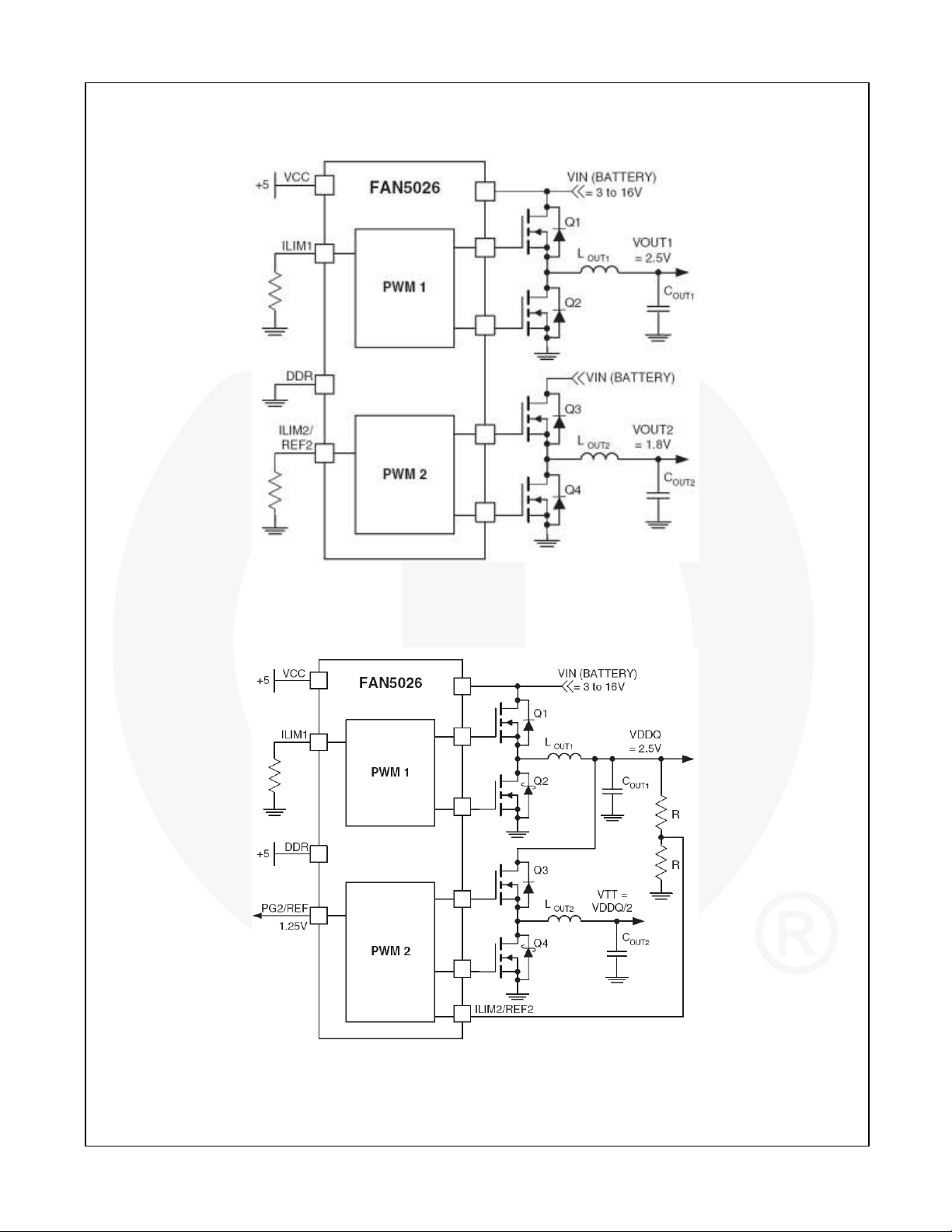
Block Diagrams
FAN5026 — Dual DDR / Dual-Output PWM Controller
Figure 1. Dual-Output Regulator
Figure 2. Typical Application
© 2005 Fairchild Semiconductor Corporation www.fairchildsemi.com
FAN5026 • Rev. 1.0.8 2
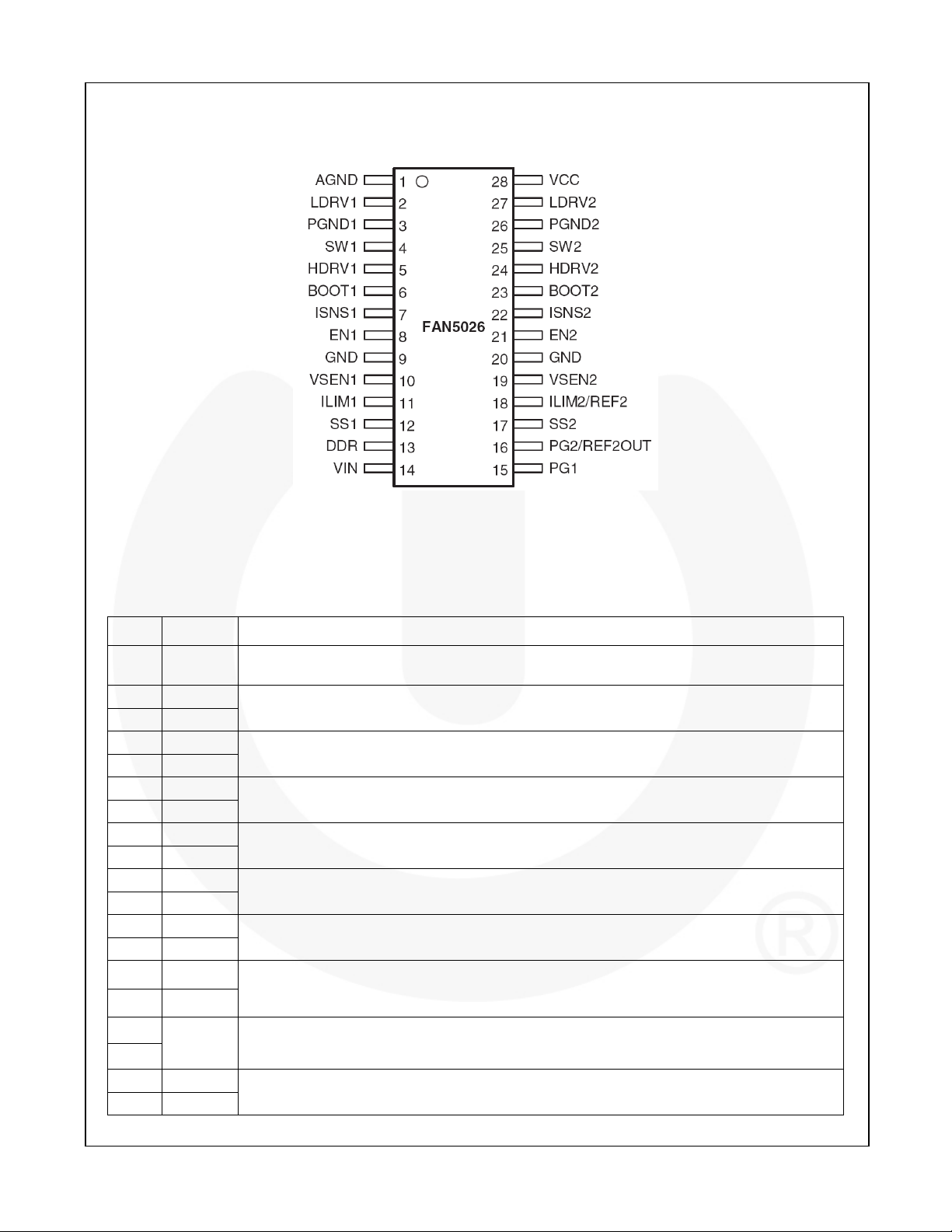
Pin Configuration
FAN5026 — Dual DDR / Dual-Output PWM Controller
Figure 3. TSSOP-28
Pin Definitions
Pin # Name Description
1 AGND
2 LDRV1
27 LDRV2
3 PGND1
26 PGND2
4 SW1
25 SW 2
5 HDRV1
24 HDRV2
6 BOOT1
23 BOOT2
7 ISNS1
22 ISNS2
8 EN1
21 EN2
Analog Ground. This is the signal ground reference for the IC. All voltage levels are measured
with respect to this pin
Low-Side Drive. The low-side (lower) MOSFET driver output. Connect to gate of low-side
MOSFET.
Power Ground. The return for the low-side MOSFET driver. Connect to source of low-side
MOSFET.
Switching Node. Return for the high-side MOSFET driver and a current sense input. Connect
to source of high-side MOSFET and low-side MOSFET drain.
High-Side Drive. High-side (upper) MOSFET driver output. Connect to gate of high-side
MOSFET.
BOOT. Positive supply for the upper MOSFET driver. Connect as shown in Figure 4.
Current-Sense Input. Monitors the voltage drop across the lower MOSFET or external sense
resistor for current feedback.
Enable. Enables operation when pulled to logic HIGH. Toggling EN resets the regulator after a
latched fault condition. These are CMOS inputs whose state is indeterminate if left open.
9
20
10 VSEN1
19 VSEN2
© 2005 Fairchild Semiconductor Corporation www.fairchildsemi.com
FAN5026 • Rev. 1.0.8 3
GND
Ground
Output Voltage Sense. The feedback from the outputs; used for regulation as well as PG,
under-voltage, and over-voltage protection and monitoring.
Continued on the following page…
Pin Definitions
Pin # Name Description
11 ILIM1
12 SS1
17 SS2
13 DDR
14 VIN
15 PG1
16
18
PG2 /
REF2OUT
ILIM2 /
REF2
28 VCC
Current Limit 1. A resistor from this pin to GND sets the current limit.
Soft Start. A capacitor from this pin to GND programs the slew rate of the converter during
initialization. During initialization, this pin is charged with a 5mA current source.
DDR Mode Control. HIGH = DDR Mode. LOW = two separate regulators operating 180
degrees out of phase.
Input Voltage. Normally connected to the battery, providing voltage feedforward to set the
amplitude of the internal oscillator ramp. When using the IC for two-step conversion from 5V
input, connect through 100KΩ resistor to ground, which sets the appropriate ramp gain and
synchronizes the channels 90° out of phase.
Power-Good Flag. An open-drain output that pulls LOW when V
the 0.9V reference.
Power-Good 2. When not in DDR Mode, open-drain output that pulls LOW when the V
out of regulation or in a fault condition.
Reference Out 2. When in DDR Mode, provides a buffered output of REF2. Typically used as
the V
reference.
DDQ/2
Current Limit 2. When not in DDR Mode, a resistor from this pin to GND sets the current limit.
Reference for reg #2 when in DDR Mode. Typically set to V
VCC. This pin powers the chip as well as the LDRV buffers. The IC starts to operate when
voltage on this pin exceeds 4.6V (UVLO rising) and shuts down when it drops below 4.3V
(UVLO falling).
OUT1/2
is outside a ±10% range of
SEN
OUT
.
FAN5026 — Dual DDR / Dual-Output PWM Controller
is
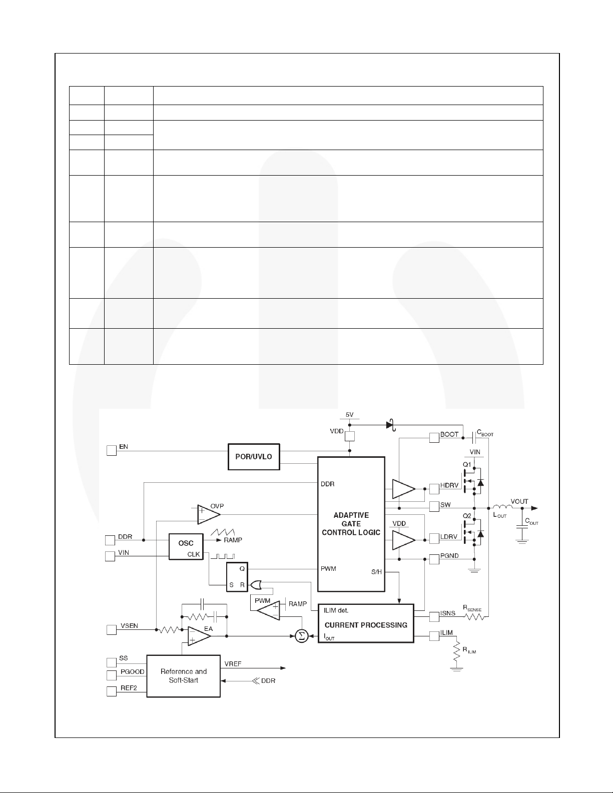
Block Diagram
Figure 4. IC Block Diagram
© 2005 Fairchild Semiconductor Corporation www.fairchildsemi.com
FAN5026 • Rev. 1.0.8 4
Absolute Maximum Ratings
Stresses exceeding the absolute maximum ratings may damage the device. The device may not function or be
operable above the recommended operating conditions and stressing the parts to these levels is not recommended.
In addition, extended exposure to stresses above the recommended operating conditions may affect device
reliability. The absolute maximum ratings are stress ratings only.
Symbol Parameter Min. Max. Unit
VCC VCC Supply Voltage 6.5 V
VIN VIN Supply Voltage 18 V
BOOT, SW, ISNS, HDRV 24 V
BOOTx to SWx 6.5 V
All Other Pins -0.3 VCC+0.3 V
TJ Junction Temperature -40 +150 ºC
T
Storage Temperature -65 +150 ºC
STG
TL Lead Temperature (Soldering,10 Seconds) +300 ºC
FAN5026 — Dual DDR / Dual-Output PWM Controller
Recommended Operating Conditions
The Recommended Operating Conditions table defines the conditions for actual device operation. Recommended
operating conditions are specified to ensure optimal performance to the datasheet specifications. Fairchild does not
recommend exceeding them or designing to Absolute Maximum Ratings.
Symbol Parameter Min. Typ. Max. Unit
VCC VCC Supply Voltage 4.75 5.00 5.25 V
VIN VIN Supply Voltage 16 V
TA Ambient Temperature -40 +85 °C
ΘJA Thermal Resistance, Junction to Ambient 90 °C/W
© 2005 Fairchild Semiconductor Corporation www.fairchildsemi.com
FAN5026 • Rev. 1.0.8 5
Electrical Characteristics
Recommended operating conditions, unless otherwise noted.
Symbol Parameter Conditions Min. Typ. Max. Units
Power Supplies
LDRV, HDRV Open, V
I
VCC
V
Current
CC
Above Regulation Point
Shutdown (EN-0) 30 µA
I
SINK
I
SOURCE
V
Current, Sinking VIN = 15V 10 30 µA
IN
VIN Current, Sourcing VIN = 0V -15 -30 µA
ISD VIN Current, Shutdown 1 µA
V
UVLO Threshold
UVLO
V
UVLO Hysteresis 300 mV
UVLOH
Rising VCC 4.30 4.55 4.75 V
Falling 4.10 4.25 4.45 V
Oscillator
f
Frequency 255 300 345 KHz
osc
VPP Ramp Amplitude
V
Ramp Offset 0.5 V
RAMP
G Ramp / VIN Gain
VIN = 16V 2 V
VIN = 5V 1.25 V
VIN ≤ 3V
1V < VIN < 3V 250 mV/V
Reference and Soft-Start
V
Internal Reference Voltage 0.891 0.900 0.909 V
REF
ISS Soft-Start Current At Startup 5 µA
VSS Soft-Start Complete Threshold 1.5 V
PWM Converters
Load Regulation I
I
SEN
UVLO
V
TSD
Bias Current 50 80 120 nA
SEN
Under-Voltage Shutdown % of Set Point, 2µs Noise Filter 70 75 80 %
from 0 to 5A, VIN from 5 to 15V -2 +2 %
OUTX
UVLO Over-Voltage Threshold % of Set Point, 2µs Noise Filter 115 120 125 %
I
Over-Current Threshold
SNS
R
= 68.5KΩ, Figure 12
ILIM
Minimum Duty Cycle 10 %
Output Drivers
HDRV Output Resistance
LDRV Output Resistance
Sourcing 12 15
Sinking 2.4 4.0
Sourcing 12 15
Sinking 1.2 2.0
Power-Good Output and Control Pins
Lower Threshold % of Set Point, 2µs Noise Filter -86 -94 %
Upper Threshold % of Set Point, 2µs Noise Filter 108 116 %
PG Output Low IPG = 4mA 0.5 V
Leakage Current V
PG2/REF2OUT Voltage
= 5V 1 µA
PULLUP
DDR = 1, 0 mA < I
DDR, EN Inputs
V
Input High 2 V
INH
V
Input Low 0.8 V
INL
SEN
REF2OUT
Forced
≤10mA
2.2 3.0 µA
125 mV/V
112 140 168 µA
Ω
Ω
99.00 1.01
V
%
REF2
FAN5026 — Dual DDR / Dual-Output PWM Controller
© 2005 Fairchild Semiconductor Corporation www.fairchildsemi.com
FAN5026 • Rev. 1.0.8 6

Typical Application
FAN5026 — Dual DDR / Dual-Output PWM Controller
Figure 5. DDR Regulator Application
Table 1. DDR Regulator BOM
Description Qty.
Capacitor 68µf, Tantalum, 25V, ESR 150mΩ
Capacitor 10nf, Ceramic 2 C2, C3 Any
Capacitor 68µf, Tantalum, 6V, ESR 1.8Ω
Capacitor 150nF, Ceramic 2 C5, C7 Any
Capacitor 180µf, Specialty Polymer 4V, ESR 15mΩ
Capacitor 1000µf, Specialty Polymer 4V, ESR 10mΩ
Capacitor 0.1µF, Ceramic 2 C9 Any
1.82KΩ, 1% Resistor
56.2KΩ, 1% Resistor
10KΩ, 5% Resistor
3.24KΩ, 1% Resistor
1.5KΩ, 1% Resistor
Schottky Diode 30V 2 D1, D2 Fairchild Semiconductor BAT54
Inductor 6.4µH, 6A, 8.64mΩ
Inductor 0.8µH, 6A, 2.24mΩ
Dual MOSFET with Schottky 2 Q1, Q2 Fairchild Semiconductor FDS6986AS
DDR Controller 1 U1 Fairchild Semiconductor FAN5026
Notes:
1. C6 = 2 X 180µF in parallel.
2. Suitable for typical notebook computer application of 4A continuous, 6A peak for V
above 6A is required, use single SO-8 packages. For more information, refer to the Power MOSFET Selection
Section and use AN-6002 for design calculations.
1 C1 AVX TPSV686*025#0150
1 C4 AVX TAJB686*006
2 C6A, C6B
1 C8 Kemet T510E108(1)004AS4115
3 R1, R2, R3 Any
1 R3 Any
2 R4 Any
1 R5 Any
2 R7, R8 Any
1
1 L2 Panasonic ETQ-P6F0R8LFA
Ref. Vendor Part Number
(1)
Panasonic EEFUE0G181R
L1 Panasonic ETQ-P6F6R4HFA
. If continuous operation
DDQ
(2)
© 2005 Fairchild Semiconductor Corporation www.fairchildsemi.com
FAN5026 • Rev. 1.0.8 7

FAN5026 — Dual DDR / Dual-Output PWM Controller
Typical Applications
(Continued)
Figure 6. Dual Regulator Application
Table 2. Dual Regulator BOM
Description Qty.
Capacitor 68µf, Tantalum, 25V, ESR 95mΩ
Capacitor 10nf, Ceramic 2 C2, C3 Any
Capacitor 68µf, Tantalum, 6V, ESR 1.8Ω
Capacitor 150nF, Ceramic 2 C5, C7 Any
Capacitor 330µf, Poscap, 4V, ESR 40mΩ
Capacitor 0.1µF, Ceramic 2 C9 Any
56.2KΩ, 1% Resistor
10KΩ, 5% Resistor
3.24KΩ, 1% Resistor
1.82KΩ, 1% Resistor
1.5KΩ, 1% Resistor
Schottky Diode 30V 2 D1, D2 Fairchild Semiconductor BAT54
Inductor 6.4µH, 6A, 8.64mΩ
Dual MOSFETs with Schottky 1 Q1, Q2 Fairchild Semiconductor FDS6986AS
DDR Controller 1 U1 Fairchild Semiconductor FAN5026
1 C1 AVX TPSV686*025#095
1 C4 AVX TAJB686*006
2 C6, C8 Sanyo 4TPB330ML
1 R1, R2 Any
1 R3 Any
1 R4 Any
3 R5, R8, R9 Any
2 R6, R7 Any
2 L1, L2 Panasonic ETQ-P6F6R4HFA
Ref. Vendor Part Number
(3)
Note:
3. If currents above 4A continuous are required, use single SO-8 packages. For more information, refer to the
Power MOSFET Selection Section and AN-6002 for design calculations.
© 2005 Fairchild Semiconductor Corporation www.fairchildsemi.com
FAN5026 • Rev. 1.0.8 8

V
V
V
Circuit Description
FAN5026 — Dual DDR / Dual-Output PWM Controller
Overview
The FAN5026 is a multi-mode, dual-channel PW M
controller intended for graphic chipset, SDRAM, DDR
DRAM, or other low-voltage power applications in
modern notebook, desktop, and sub-notebook PCs.
The IC integrates control circuitry for two synchronous
buck converters. The output voltage of each controller
can be set in the range of 0.9V to 5.5V by an external
resistor divider.
The two synchronous buck converters can operate from
an unregulated DC source (such as a notebook
battery), with voltage ranging from 5.0V to 16V, or from
a regulated system rail of 3.3V to 5.0V. In either mode,
the IC is biased from a +5V source. The PWM
modulators use an average current-mode control with
input voltage feedforward for simplified feedback loop
compensation and improved line regulation. Both PW M
controllers have integrated feedback loop compensation
that reduces the external components needed.
The FAN5026 can be configured to operate as a
complete DDR solution. When the DDR pin is set HIGH,
the second channel provides the capability to track the
output voltage of the first channel. The PWM2 converter
is prevented from going into Hysteretic Mode if the DDR
pin is HIGH. In DDR Mode, a buffered reference voltage
(buffered voltage of the REF2 pin), required by DDR
memory chips, is provided by the PG2 pin.
Converter Modes and Synchronization
Table 3. Converter Modes and Synchronization
PWM 2
w.r.t.
PWM1
converter
DDQ
Mode VIN
VIN
Pin
DDR
Pin
DDR1 Battery VIN HIGH IN PHASE
DDR2 +5V
R to
GND
HIGH +90°
DUAL ANY VIN LOW +180°
When used as a dual converter, as shown in Figure 6,
out-of-phase operation with 180-degree phase shift
reduces input current ripple.
For “two-step” conversion (where the VTT is converted
from V
as in Figure 5) used in DDR Mode, the duty
DDQ
cycle of the second converter is nominally 50% and the
optimal phasing depends on VIN. The objective is to
keep noise generated from the switching transition in
one converter from influencing the "decision" to switch
in the other converter.
When V
is from the battery, it’s typically higher than
IN
7.5V. As shown in Figure 7, 180° operation is
undesirable because the turn-on of the V
occurs very near the decision point of the VTT converter.
CLK
D DQ
V
TT
Figure 7. Noise-Susceptible 180° Phasing
for DDR1
In-phase operation is optimal to reduce inter-converter
interference when VIN is higher than 5V, (when VIN is
from a battery), as shown in Figure 8. Because the duty
cycle of PWM1 (generating V
) is short, the switching
DDQ
point occurs far away from the decision point for the VTT
regulator, whose duty cycle is nominally 50%.
CLK
V
DDQ
V
TT
Figure 8. Optimal In-Phase Operation for DDR1
When VIN ≈ 5V, 180° phase-shifted operation can be
rejected for the reasons demonstrated in Figure 7.
In-phase operation with VIN ≈ 5V is even worse, since
the switch point of either converter occurs near the
switch point of the other converter, as seen in Figure 9.
In this case, as VIN is a little higher than 5V, it tends to
cause early termination of the VTT pulse width.
Conversely, the VTT switch point can cause early
termination of the V
pulse width when VIN is slightly
DDQ
lower than 5V.
CLK
DDQ
V
TT
Figure 9. Noise-Susceptible In-Phase Operation
for DDR2
These problems are solved by delaying the second
converter’s clock by 90°, as shown in Figure 10. In this
way, all switching transitions in one converter take place
far away from the decision points of the other converter.
CLK
DDQ
V
TT
Figure 10. Optimal 90° Phasing for DDR2
© 2005 Fairchild Semiconductor Corporation www.fairchildsemi.com
FAN5026 • Rev. 1.0.8 9

ܴ
ܵܧܰܵܧ
=
ܫ
ܮܱܣܦ(ܯܣܺ
)
∙
ܴ
ܦܵ(ܱܰ
)
∙4.1ܭ
30%∙0.
125∙ܸ
ܫܰ(ܯܣܺ
)
−
100
ܴ
ܵܧܰܵܧ
=
ܫ
ܮܱܣܦ(ܯܣܺ
)
∙
ܴ
ܦܵ(ܱܰ
)
150µܣ
−
100
ܫܵܰܵ
9
=
4
3
ܫܮܫܯ
ݎ
ܫܵܰܵ
=12∙
ܫܮܫܯ
ܫܵܰܵ
=
ܫ
ܮܱܣܦ
∙
ܴ
ܦܵ(ܱܰ
)
100+ܴ
ܵܧܰܵܧ
ܫܵܰܵ
=12∙
0.9
ܴ
ܫܮܫܯ
=
10.8
ܴ
ܫܮܫܯ
ܫ
ܮܱܣܦ
=
10.8
ܴ
ܫܮܫܯ
∙
100+ܴ
ܵܧܰܵܧ
ܴ
ܦܵ(ܱܰ
)
ܴ
ܫܮܫܯ
=
10.8
ܫ
ܮܫܯܫܶ
∙
100+ܴ
ܵܧܰܵܧ
ܴ
ܦܵ(ܱܰ
)
Q2
FAN5026 — Dual DDR / Dual-Output PWM Controller
Initialization and Soft Start
Assuming EN is HIGH, FAN5026 is initialized when VCC
exceeds the rising UVLO threshold. Should VCC drop
below the UVLO threshold, an internal power-on reset
function disables the chip.
The voltage at the positive input of the error amplifier is
limited by the voltage at the SS pin, which is charged
with a 5µA current source. Once CSS has charged to
V
(0.9V) the output voltage is in regulation. The time
REF
it takes SS to reach 0.9V is:
xC9.0
t
=
9.0
where t
SS
5
is in seconds if CSS is in µF.
0.9
(1)
When SS reaches 1.5V, the power-good outputs are
enabled and Hysteretic Mode is allowed. The converter
is forced into PW M Mode during soft-start.
Current Processing Section
The following discussion refers to Figure 12.
The current through the R
sampled (typically 400ns) after Q2 is turned on, as
shown in Figure 12. That current is held and summed
with the output of the error amplifier. This effectively
creates a current-mode control loop. The resistor
connected to ISNSx pin (R
SENSE
current feedback loop. For stable operation, the voltage
induced by the current feedback at the PW M
comparator input should be set to 30% of the ramp
amplitude at maximum load current and line voltage.
The following expression estimates the recommended
value of R
current (I
R
:
DS(ON)
R
must, however, be kept higher than:
SENSE
as a function of the maximum load
SENSE
LOAD(MAX)
) and the value of the MOSFET
resistor (I
SENSE
SNS
) sets the gain in the
) is
(2a)
Since
(3b)
and at the ILIM 0.9V threshold:
(3c)
therefore:
(3d)
Current limit (I
) should be set high enough to allow
LIMIT
inductor current to rise in response to an output load
transient. Typically, a factor of 1.2 is sufficient. In
addition, since I
multiply I
LOAD(MAX)
25%). For example, in Figure 6, the target for I
I
> 1.2 x 1.25 x 1.6 x 2A ≈ 5A
LIMIT
is a peak current cut-off value,
LIMIT
by the inductor ripple current (e.g.
:
LIMIT
(4)
Since the tolerance on the current limit is largely
dependent on the ratio of the external resistors, it is
fairly accurate if the voltage drop on the switching-node
side of R
is an accurate representation of the load
SENSE
current. W hen using the MOSFET as the sensing
element, the variation of R
variation in the I
. This value varies from device to
SNS
causes proportional
DS(ON)
device and has a typical junction temperature
coefficient of about 0.4%/°C (consult the MOSFET
datasheet for actual values), so the actual current limit
set point decreases proportional to increasing MOSFET
die temperature. A factor of 1.6 in the current limit set
point should compensate for MOSFET R
DS(ON)
variations, assuming the MOSFET heat sinking keeps
its operating die temperature below 125°C.
(2b)
LDRV
R
The 100Ω is the internal resistor in series with the
ISNSx pins and has ±15% typical variation. Because
R
is in series with the internal 100Ω resistor, the
SENSE
gain in the current feedback loop and the current limit
accuracy is affected if R
is close to 100Ω.
SENSE
Setting the Current Limit
A ratio of I
when a 0.9V internal reference drives the ILIM pin. The
threshold is determined as follows:
is compared to the current established
SNS
Figure 11. Improving Current-Sensing Accuracy
More accurate sensing can be achieved by using a
resistor (R1) instead of the R
ISNS
PGND
SENSE
R1
of the FET, as shown
DS(ON)
in Figure 11. This approach causes higher losses, but
(3a)
yields greater accuracy in both V
DROOP
and I
LIMIT
. R1 is a
low value resistor (e.g. 10mΩ).
© 2005 Fairchild Semiconductor Corporation www.fairchildsemi.com
FAN5026 • Rev. 1.0.8 10

Duty Cycle Clamp
During severe load increase, the error amplifier output
can go to its upper limit, pushing a duty cycle to almost
100% for significant amount of time. This could cause a
large increase of the inductor current and lead to a long
recovery from a transient, over-current condition, or
even to a failure at especially high input voltages. To
prevent this, the output of the error amplifier is clamped
to a fixed value after two clock cycles if severe output
voltage excursion is detected, limiting the maximum
duty cycle to:
DC
MAX
V
OUT
V
IN
4.2
+=
V
IN
(5)
This is designed to not interfere with normal PWM
operation. When FPWM is grounded, the duty cycle
clamp is disabled and the maximum duty cycle is 87%.
FAN5026 — Dual DDR / Dual-Output PWM Controller
Figure 12. Current Limit / Summing Circuits
Gate Driver Section
The adaptive gate control logic translates the internal
PWM control signal into the MOSFET gate drive
signals, providing necessary amplification, level shifting,
and shoot-through protection. Also, it has functions that
optimize the IC performance over a wide range of
operating conditions. Since MOSFET switching time
can vary dramatically from type to type and with the
input voltage, the gate control logic provides adaptive
dead time by monitoring the gate-to-source voltages of
both upper and lower MOSFETs. The lower MOSFET
drive is not turned on until the gate-to-source voltage of
the upper MOSFET has decreased to less than
approximately 1V. Similarly, the upper MOSFET is not
turned on until the gate-to-source voltage of the lower
MOSFET has decreased to less than approximately 1V.
This allows a wide variety of upper and lower MOSFETs
to be used without a concern for simultaneous
conduction or shoot-through.
There must be a low-resistance, low-inductance path
between the driver pin and the MOSFET gate for the
adaptive dead-time circuit to function properly. Any
delay along that path subtracts from the delay
generated by the adaptive dead-time circuit and shootthrough may occur.
Frequency Loop Compensation
Due to the implemented current-mode control, the
modulator has a single-pole response with -1 slope at
frequency determined by load:
fπ=
PO
where RO is load resistance; CO is load capacitance.
1
CR2
OO
(6)
© 2005 Fairchild Semiconductor Corporation www.fairchildsemi.com
FAN5026 • Rev. 1.0.8 11

)
For this type of modulator, a Type-2 compensation
circuit is usually sufficient. To reduce the number of
external components and simplify the design, the PWM
controller has an internally compensated error amplifier.
Figure 13 shows a Type-2 amplifier and its response
with the responses of a current-mode modulator and
the converter. The Type-2 amplifier, in addition to the
pole at the origin, has a zero-pole pair that causes a flat
gain region at frequencies between zero and the pole.
f
Z
f
P
1
π
1
CR2
π
CR2
22
==
12
==
kHz6
600kHz
(7)
(8)
This region is also associated with phase “bump” or
reduced phase shift. The amount of phase-shift
reduction depends on the width of the region of flat gain
and has a maximum value of 90°. To further simplify the
converter compensation, the modulator gain is kept
independent of the input voltage variation by providing
feedforward of VIN to the oscillator ramp.
The zero frequency, the amplifier high-frequency gain,
and the modulator gain are chosen to satisfy most
typical applications. The crossover frequency appears
at the point where the modulator attenuation equals the
amplifier high-frequency gain. The system designer
must specify the output filter capacitors to position the
load main pole somewhere within a decade lower than
the amplifier zero frequency. W ith this type of
compensation, plenty of phase margin is achieved due
to zero-pole pair phase “boost.”
C2
C1
R2
R1
V
IN
EA Out
f
Z
f
P
18
14
0
e
r
r
o
r
a
m
modul ator
REF
C
o
n
v
e
r
t
e
p
r
f
P0
If a larger inductor value or low-ESR values are
required by the application, additional phase margin can
be achieved by putting a zero at the LC crossover
frequency. This can be achieved with a capacitor across
the feedback resistor (e.g. R5 from Figure 6), as shown
in Figure 14.
L(OUT)
VSEN
R6
V
OUT
C(OUT
C(Z)R5
Figure 14. Improving Phase Margin
The optimal value of C(Z) is:
C(Z)×=
C(OUT)L(OUT)
R
(9)
Protections
The converter output is monitored and protected
against extreme overload, short-circuit, over-voltage,
and under-voltage conditions.
A sustained overload on an output sets the PGx pin
LOW and latches-off the regulator on which the fault
occurs. Operation can be restored by cycling the VCC
voltage or by toggling the EN pin.
If V
drops below the under-voltage threshold, the
OUT
regulator shuts down immediately.
Over-Current Sensing
If the circuit’s current-limit signal (“ILIM det” in Figure
12) is HIGH at the beginning of a clock cycle, a pulseskipping circuit is activated and HDRV is inhibited. The
circuit continues to pulse skip in this manner for the
next eight clock cycles. If, at any time from the ninth to
the sixteenth clock cycle, the ILIM det is again reached;
the over-current protection latch is set, disabling the
regulator. If ILIM det does not occur between cycles
nine and sixteen, normal operation is restored and the
over-current circuit resets itself.
FAN5026 — Dual DDR / Dual-Output PWM Controller
Figure 13. Compensation
Conditional stability may occur only when the main load
pole is positioned too much to the left on the frequency
axis due to excessive output filter capacitance. In this
case, an ESR zero placed within the 10kHz to 50kHz
range gives some additional phase boost. Fortunately,
there is an opposite trend in mobile applications to keep
the output capacitor as small as possible.
Figure 15. Over-Current Protection Waveforms
© 2005 Fairchild Semiconductor Corporation www.fairchildsemi.com
FAN5026 • Rev. 1.0.8 12

(
)
(
)
∆
Over-Voltage / Under-Voltage Protection
Should the V
voltage exceed 120% of V
SNS
REF
(0.9V)
due to an upper MOSFET failure or for other reasons,
Similarly, if an output short-circuit or severe load
transient causes the output to drop to less than 75% of
the regulation set point, the regulator shuts down.
the over-voltage protection comparator forces LDRV
HIGH. This action actively pulls down the output voltage
and, in the event of the upper MOSFET failure,
eventually blows the battery fuse. As soon as the output
voltage drops below the threshold, the OVP comparator
is disengaged.
This OVP scheme provides a ”soft” crowbar function,
which accommodates severe load transients and does
Over-Temperature Protection
The chip incorporates an over-temperature protection
circuit that shuts the chip down if a die temperature of
about 150°C is reached. Normal operation is restored at
die temperature below 125°C with internal power-on
reset asserted, resulting in a full soft-start cycle.
not invert the output voltage when activated —
a common problem for latched OVP schemes.
Design and Component Selection Guidelines
As an initial step, define the operating input voltage
range, output voltage, and minimum and maximum load
currents for the controller.
Setting the Output Voltage
The internal reference voltage is 0.9V. The output is
divided down by a voltage divider to the VSEN pin (for
example, R5 and R6 in Figure 5). The output voltage
therefore is:
for this example, use:
SW
therefore:
FAN5026 — Dual DDR / Dual-Output PWM Controller
5.2V,12V
==
OUTIN
KHz300f
=
µH4.4L ≈
A5.1A6•%25I
==∆
(14)
(15)
OUT
−
5R
−Ω
9.0VK82.1
OUT
9.0
Ω=
(10)
(11)
V9.0
=
6R
To minimize noise pickup on this node, keep the
resistor to GND (R6) below 2K; for example, R6 at
1.82KΩ. Then choose R5:
= K24.3
5R
For DDR applications converting from 3.3V to 2.5V or
other applications requiring high duty cycles, the duty
cycle clamp must be disabled by tying the converter’s
FPWM to GND. When converter’s FPWM is at GND,
the converter’s maximum duty cycle is greater than
90%. When using as a DDR converter with 3.3V input,
set up the converter for in-phase synchronization by
tying the VIN pin to +5V.
V9.0V
Output Inductor Selection
The minimum practical output inductor value keeps the
inductor current just on the boundary of continuous
conduction at some minimum load. Industry standard
practice is to choose the minimum current somewhere
from 15% to 35% of the nominal current. At light load,
the controller can automatically switch to Hysteretic
Mode to sustain high efficiency. The following equations
select the proper value of the output filter inductor:
V
OUT
12I
×=∆
=
MIN
where ∆I is the inductor ripple current and ∆V
maximum ripple allowed:
ESR
(12)
is the
OUT
Output Capacitor Selection
The output capacitor serves two major functions in a
switching power supply. Along with the inductor, it filters
the sequence of pulses produced by the switcher and it
supplies the load transient currents. The requirements
are usually dictated by ESR, inductor ripple current (∆I),
and the allowable ripple voltage (∆V):
V
V
<
=∆
∆
I
∆
I
∆
f8C
××
SWOUT
.
ESR
In addition, the capacitor’s ESR must be low enough to
allow the converter to stay in regulation during a load
step. The ripple voltage due to ESR for the converter in
Figure 6 is 120mVPP. Some additional ripple appears
due to the capacitance value itself:
which is only about 1.5mV for the converter in Figure 6
and can be ignored.
The capacitor must also be rated to withstand the RMS
current, which is approximately 0.3 X (∆I), or about
400mA, for the converter in Figure 6. High-frequency
decoupling capacitors should be placed as close to the
loads as physically possible
(16)
(17)
Input Capacitor Selection
The input capacitor should be selected by its ripple
current rating.
VV
L ×
© 2005 Fairchild Semiconductor Corporation www.fairchildsemi.com
FAN5026 • Rev. 1.0.8 13
−
=
SW
V
OUTIN
∆×
OUT
V
If
IN
(13)

(
)
(
)
Two-Stage Converter Case
In DDR Mode (Figure 5), the VTT power input is
powered by the V
capacitor ripple current is produced by the V
output; therefore all of the input
DDQ
DDQ
converter. A conservative estimate of the output current
required for the 2.5V regulator is:
I
II
VDDQREGI
VTT
+=
2
As an example, if the average I
I
is 1A, I
VTT
current is about 3.5A. If average input
VDDQ
is 3A and average
VDDQ
(18)
voltage is 16V, RMS input ripple current is:
2
DDII −=
)MAX(OUTRMS
(19)
where D is the duty cycle of the PWM1 converter and:
V
OUT
D
V
IN
5.2
=<
12
(20)
therefore:
2
5.2
RMS
5.2
5.3I
−=
12
12
=
A42.1
(21)
Dual Converter 180° Phased
In Dual Mode (shown in Figure 5), both converters
contribute to the capacitor input ripple current. W ith
each converter operating 180° out of phase, the RMS
currents add in the following fashion:
2
+=
)1(RMSRMS
2
( )
1RMS
11
which, for the dual 3A converters of Figure 6, calculates:
2
or III
)2(RMS
( )
2
2
DDIDDII −+−=
2
(22)
2
(23)
22
(QG). C
= CGD + CGS and it controls t1, t2, and t4
ISS
timing. CGD receives the current from the gate driver
during t3 (as VDS is falling). The gate charge (QG)
parameters on the lower graph are either specified in or
can be derived from MOSFET datasheets.
Assuming switching losses are about the same for both
the rising edge and falling edge, Q1’s switching losses
occur during the shaded time when the MOSFET has
voltage across it and current through it.
These losses are given by:
PPP +=
CONDSWUPPER
IV
×
P
P
SW
COND
=
LDS
2
V
OUT
V
IN
f t2
××
s
SW
2
RI
××=
)ON(DSOUT
where:
P
is the upper MOSFET’s total losses and P
UPPER
and P
are the switching and conduction losses for a
COND
given MOSFET;
R
is at the maximum junction temperature (TJ);
DS(ON)
and
t
is the switching period (rise or fall time), shown as t2
S
and t3 in Figure 16.
The driver’s impedance and C
determine t2, while
ISS
t3’s period is controlled by the driver’s impedance and
QGD. Since most of t
occurs when V
S
= VSP, use a
GS
constant current assumption for the driver to simplify
the calculation of tS:
C
V
DS
ISS
C
GD
C
ISS
FAN5026 — Dual DDR / Dual-Output PWM Controller
(25)
(26)
(27)
SW
A51.1I
=
RMS
Power MOSFET Selection
(24)
I
D
Losses in a MOSFET are the sum of its switching (PSW)
and conduction (P
In typical applications, the FAN5026 converter’s output
voltage is low with respect to its input voltage.
Therefore, the lower MOSFET (Q2) is conducting the
full load current for most of the cycle. Q2 should
therefore be selected to minimize conduction losses,
thereby selecting a MOSFET with low R
In contrast, the high-side MOSFET (Q1) has a much
shorter duty cycle and it’s conduction loss has less
impact. Q1, however, sees most of the switching losses,
the primary selection criteria should be gate charge.
High-Side Losses
Figure 16 shows a MOSFET’s switching interval, with
the upper graph being the voltage and current on the
drain-to-source and the lower graph detailing VGS vs.
time with a constant current charging the gate. The X
axis, therefore, is also representative of gate charge
© 2005 Fairchild Semiconductor Corporation www.fairchildsemi.com
FAN5026 • Rev. 1.0.8 14
COND
) losses.
DS(ON)
Q
GS
V
SP
V
TH
V
.
GS
t1 t2 t3
Q
G(SW)
Q
GD
t4 t5
4.5V
Figure 16. Switching Losses and QG
5V
C
R
D
HDRV
SW
R
GATE
G
C
GS
VIN
GD
Figure 17. Drive Equivalent Circuit

FAN5026 — Dual DDR / Dual-Output PWM Controller
Q
)SW(G
I
DRIVER
==
t
s
Most MOSFET vendors specify QGD and Q
Q
)SW(G
−
+
VV
SPCC
RR
GATEDRIVER
GS.
Q
(28)
G(SW)
can be determined as:
QQQQ −+=
THGSGD)SW(G
(29)
where QTH is the gate charge required to get the
MOSFET to it’s threshold (VTH).
For the high-side MOSFET, VDS = VIN, which can be as
high as 20V in a typical portable application. Care
should be taken to include the delivery of the
MOSFET’s gate power (PGATE) in calculating the
power dissipation required for the FAN5026:
G
ATE
where Q
SWCCG
is the total gate charge to reach VCC.
G
(30)
fVQP ××=
Low-Side Losses
Q2, however, switches on or off with its parallel
Schottky diode conducting, therefore VDS ≈ 0.5V. Since
PSW is proportional to VDS, Q2’s switching losses are
negligible and Q2 is selected based on R
Conduction losses for Q2 are given by:
2
RID1P
××−=
DS(ON)
)ON(DSOUTCOND
of the MOSFET at the
where R
( )
DS(ON)
is the R
highest operating junction temperature, and:
V
OUT
D =
V
IN
(32)
is the minimum duty cycle for the converter.
Since D
< 20% for portable computers, (1-D) ≈ 1
MIN
produces a conservative result, further simplifying the
calculation.
The maximum power dissipation (P
D(MAX)
the maximum allowable die temperature of the low-side
MOSFET; the ΘJA, and the maximum allowable ambient
temperature rise:
only.
DS(ON)
(31)
) is a function of
Layout Considerations
Switching converters, even during normal operation,
produce short pulses of current that could cause
substantial ringing and be a source of EMI if layout
constraints are not observed.
There are two sets of critical components in a DC-DC
converter. The switching power components process
large amounts of energy at high rates and are noise
generators. The low-power components responsible for
bias and feedback functions are sensitive to noise.
A multi-layer printed circuit board is recommended.
Dedicate one solid layer for a ground plane. Dedicate
another solid layer as a power plane and break this
plane into smaller islands of common voltage levels.
Notice all the nodes that are subjected to high-dV/dt
voltage swing; such as SW, HDRV, and LDRV. All
surrounding circuitry tends to couple the signals from
these nodes through stray capacitance. Do not oversize
copper traces connected to these nodes. Do not place
traces connected to the feedback components adjacent
to these traces. It is not recommended to use highdensity interconnect systems, or micro-vias, on these
signals. The use of blind or buried vias should be
limited to the low-current signals only. The use of
normal thermal vias is at the discretion of the designer.
Keep the wiring traces from the IC to the MOSFET gate
and source as short as possible and capable of
handling peak currents of 2A. Minimize the area within
the gate-source path to reduce stray inductance and
eliminate parasitic ringing at the gate.
Locate small critical components, like the soft-start
capacitor and current-sense resistors, as close as
possible to the respective pins of the IC.
The FAN5026 utilizes advanced packaging technology
with lead pitch of 0.6mm. High-performance analog
semiconductors utilizing narrow lead spacing may
require special considerations in design and
manufacturing. It is critical to maintain proper
cleanliness of the area surrounding these devices.
TT
P
=
)MAX(D
Θ
−
JA
)MAX(A)MAX(J
(33)
ΘJA depends primarily on the amount of PCB area that
can be devoted to heat sinking
(see Application Note
AN-1029, Maximum Power Enhancement Techniques
for SO-8 Power MOSFETs for SO-8 MOSFET thermal
information)
© 2005 Fairchild Semiconductor Corporation www.fairchildsemi.com
FAN5026 • Rev. 1.0.8 15
.

FAN5026 — Dual DDR / Dual-Output PWM Controller
Physical Dimensions
Figure 18. 28-Lead, Thin Shrink Small Outline Package (TSSOP), JEDEC MO-153, 4.4mm Wide
Package drawings are provided as a service to customers considering Fairchild components. Drawings may change in any manner
without notice. Please note the revision and/or date on the drawing and contact a Fairchild Semiconductor representative to verify
or obtain the most recent revision. Package specifications do not expand the terms of Fairchild’s worldwide terms and conditions,
specifically the warranty therein, which covers Fairchild products.
Always visit Fairchild Semiconductor’s online packaging area for the most recent package drawings:
http://www.fairchildsemi.com/packaging/.
© 2005 Fairchild Semiconductor Corporation www.fairchildsemi.com
FAN5026 • Rev. 1.0.8 16

FAN5026 — Dual DDR / Dual-Output PWM Controller
© 2005 Fairchild Semiconductor Corporation www.fairchildsemi.com
FAN5026 • Rev. 1.0.8 17
 Loading...