


Cypress Semiconductor CY7C4425-25ASC, CY7C4425-25ACT, CY7C4425-15ASC, CY7C4425-15ACT, CY7C4425-15AC Datasheet
...fax id: 5410
CY7C4425/4205/4215
CY7C4225/4235/4245
64, 256, 512, 1K, 2K, 4K x 18 Synchronous FIFOs
Features
•High-speed, low-power, first-in first-out (FIFO) memories
•64 x 18 (CY7C4425)
•256 x 18 (CY7C4205)
•512 x 18 (CY7C4215)
•1K x 18 (CY7C4225)
•2K x 18 (CY7C4235)
•4K x 18 (CY7C4245)
•High-speed 100-MHz operation (10 ns read/write cycle time)
•Low power (ICC =45 mA)
•Fully asynchronous and simultaneous read and write operation
•Empty, Full, Half Full, and Programmable Almost Empty/Almost Full status flags
•TTL-compatible
•Retransmit function
•Output Enable (OE) pin
•Independent read and write enable pins
•Center power and ground for reduced noise
•Supports free-running 50% duty cycle clock inputs
•Width Expansion Capability
•Depth Expansion Capability
•Space saving 64-pin 10x10 TQFP, and 14x14 TQFP
•68-pin PLCC
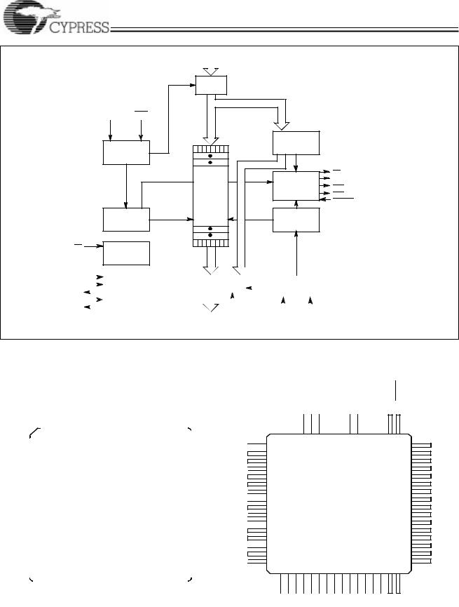
Functional Description
The CY7C42X5 are high-speed, low-power, first-in first-out (FIFO) memories with clocked read and write interfaces. All are 18 bits wide and are pin/functionally compatible to IDT722x5. The CY7C42X5 can be cascaded to increase FIFO depth. Programmable features include Almost Full/Almost Empty flags. These FIFOs provide solutions for a wide variety of data buffering needs, including high-speed data acquisition, multiprocessor interfaces, and communications buffering.
These FIFOs have 18-bit input and output ports that are controlled by separate clock and enable signals. The input port is
controlled by a free-running clock (WCLK) and a write enable pin (WEN).
When WEN is asserted, data is written into the FIFO on the rising edge of the WCLK signal. While WEN is held active, data is continually written into the FIFO on each cycle. The output port is controlled in a similar manner by a free-running read clock (RCLK) and a read enable pin (REN). In addition, the CY7C42X5 have an output enable pin (OE). The read and write clocks may be tied together for single-clock operation or the two clocks may be run independently for asynchronous read/write applications. Clock frequencies up to 100 MHz are achievable.
Retransmit and Synchronous Almost Full/Almost Empty flag features are available on these devices.
Depth expansion is possible using the cascade input (WXI, RXI), cascade output (WXO, RXO), and First Load (FL) pins. The WXO and RXO pins are connected to the WXI and RXI pins of the next device, and the WXO and RXO pins of the last device should be connected to the WXI and RXI pins of the first device. The FL pin of the first device is tied to VSS and the
FL pin of all the remaining devices should be tied to VCC.
The CY7C42X5 provides five status pins. These pins are decoded to determine one of five states: Empty, Almost Empty, Half Full, Almost Full, and Full (see Table 2). The Half Full flag shares the WXO pin. This flag is valid in the standalone and width-expansion configurations. In the depth expansion, this pin provides the expansion out (WXO) information that is used to signal the next FIFO when it will be activated.
The Empty and Full flags are synchronous, i.e., they change state relative to either the read clock (RCLK) or the write clock (WCLK). When entering or exiting the Empty states, the flag is updated exclusively by the RCLK. The flag denoting Full states is updated exclusively by WCLK. The synchronous flag architecture guarantees that the flags will remain valid from one clock cycle to the next. As mentioned previously, the Almost Empty/Almost Full flags become synchronous if the VCC/SMODE is tied to VSS. All configurations are fabricated using an advanced 0.65μ N-Well CMOS technology. Input ESD protection is greater than 2001V, and latch-up is prevented by the use of guard rings.
Cypress Semiconductor Corporation • 3901 North First Street • San Jose • CA 95134 • 408-943-2600 April 1995 - Revised August 18, 1997
CY7C4425/4205/4215
CY7C4225/4235/4245
D0 – 17
Logic Block Diagram
|
|
INPUT |
|
|
|
|
REGISTER |
|
|
|
WCLK |
WEN |
|
|
|
|
|
FLAG |
|
|
WRITE |
|
PROGRAM |
|
|
|
REGISTER |
|
|
|
CONTROL |
|
|
|
|
|
DUAL PORT |
|
FF |
|
|
RAM ARRAY |
FLAG |
EF |
|
|
64 x 18 |
PAE |
|
|
|
LOGIC |
||
|
|
256 x 18 |
PAF |
|
|
|
|
||
|
|
512 x 18 |
|
|
|
|
|
SMODE |
|
|
|
1K x 18 |
|
|
|
WRITE |
2K x 18 |
READ |
|
|
4K x 18 |
|
||
|
|
POINTER |
|
|
|
POINTER |
|
||
RS |
RESET |
|
|
|
|
|
|
|
|
|
LOGIC |
|
|
|
|
|
|
|
|
|
|
|
|
|
|
|
|
|
|
|
|
|
|
|
|
|
|
|
|
FL/RT |
|
|
|
THREE–STATE |
|
|
|
|
READ |
|
|
|
|
|||||||||
|
|
|
|
|
|
|
|
|
|
|
|
|
|
|
|
|
|
||||||
|
|
WXI |
|
EXPANSION |
|
OUTPUT REGISTER |
|
|
|
|
|
|
|
|
|||||||||
|
|
|
|
|
|
|
|
CONTROL |
|
||||||||||||||
|
|
|
|
|
|
|
|
|
|
|
|
|
|
|
|
|
|
|
|||||
WXO/HF |
|
|
|
|
|
|
|
|
|
|
|
|
|
||||||||||
|
LOGIC |
|
|
|
|
|
|
|
|
|
|
|
|
|
|
|
|||||||
|
|
|
|
|
|
|
|
|
|
|
|
|
|
|
|
|
|
|
|
|
|
|
|
|
|
|
|
RXI |
|
|
|
|
|
|
|
|
|
|
|
|
|
|
|
|
|
|
|
|
|
|
|
|
|
|
|
|
|
|
|
|
|
|
|
OE |
|
|
|
|
|
|
|
|
|
|
|
|
|
|
|
|
|
|
|
|
|
|
|
|
|
|
|||||
|
|
RXO |
|
|
|
|
|
|
|
|
|
|
|
|
|
|
|
42X5–1 |
|||||
|
|
|
|
|
|
|
|
|
|
Q0 – 17 |
|
|
|
|
|
|
|
|
|||||
|
|
|
|
|
|
|
|
|
|
|
|
|
|
|
|
|
|
|
|||||
|
|
|
|
|
|
|
|
|
|
|
|
|
RCLK |
REN |
|||||||||
|
|
|
|
|
|
|
|
|
|
|
|
|
|
|
|
|
|
||||||
Pin Configurations
PLCC
Top View
|
|
|
|
|
D |
D |
D |
GND |
|
RCLK |
REN |
|
LD |
OE |
RS |
V GND |
EF |
V |
Q |
|
Q |
GND |
Q |
|
|
|
|
|
|
|
|
|||||||||||||||
|
|
|
15 |
16 |
17 |
|
|
|
|
|
|
|
|
|
|
|
|
|
CC |
|
|
CC |
17 |
16 |
|
|
15 |
|
|
|
|
|
|
|
|
|||||||||||
|
|
|
|
|
|
|
|
|
|
|
|
|
|
|
|
|
|
|
|
|
|
|
|
|
|
|
|
|
||||||||||||||||||
|
|
|
|
|
|
|
|
|
|
|
|
|
|
|
|
|
|
|
|
|
|
|
|
|
|
|
|
|
|
|
|
|
|
|
|
|
|
|
|
|
|
|
|
|
|
|
D14 |
|
9 |
|
8 |
|
7 |
|
6 |
5 |
|
4 |
|
3 |
|
2 |
|
1 |
|
68 67 66 65 64 63 62 61 |
|
|
|
VCC |
|
|
|
|
|||||||||||||||||||
|
|
|
|
|
|
|||||||||||||||||||||||||||||||||||||||||
|
10 |
|
|
|
|
|
|
|
|
|
|
|
|
|
|
|
|
|
|
|
|
|
|
|
|
|
|
|
|
|
|
|
|
|
|
60 |
|
|
|
|
|
|
||||
|
|
|
|
|
|
|
|
|
|
|
|
|
|
|
|
|
|
|
|
|
|
|
|
|
|
|
|
|
|
|
|
|
|
|
|
|
/SMODE |
|
D15 |
|
||||||
D13 |
|
11 |
|
|
|
|
|
|
|
|
|
|
|
|
|
|
|
|
|
|
|
|
|
|
|
|
|
|
|
|
|
|
|
|
|
|
59 |
|
|
Q14 |
|
|||||
D12 |
|
12 |
|
|
|
|
|
|
|
|
|
|
|
|
|
|
|
|
|
|
|
|
|
|
|
|
|
|
|
|
|
|
|
|
|
|
58 |
|
|
Q13 |
D14 |
|
||||
|
|
|
|
|
|
|
|
|
|
|
|
|
|
|
|
|
|
|
|
|
|
|
|
|
|
|
|
|
|
|
|
|
|
|
|
|
|
|||||||||
D11 |
|
13 |
|
|
|
|
|
|
|
|
|
|
|
|
|
|
|
|
|
|
|
|
|
|
|
|
|
|
|
|
|
|
|
|
|
|
57 |
|
|
GND |
D13 |
|
||||
|
|
|
|
|
|
|
|
|
|
|
|
|
|
|
|
|
|
|
|
|
|
|
|
|
|
|
|
|
|
|
|
|
|
|
|
|
|
|||||||||
D10 |
|
14 |
|
|
|
|
|
|
|
|
|
|
|
|
|
|
|
|
|
|
|
|
|
|
|
|
|
|
|
|
|
|
|
|
|
|
56 |
|
|
Q12 |
D12 |
|
||||
|
|
|
|
|
|
|
|
|
|
|
|
|
|
|
|
|
|
|
|
|
|
|
|
|
|
|
|
|
|
|
|
|
|
|
|
|
|
|||||||||
|
|
|
|
|
|
|
|
|
|
|
|
|
|
CY7C4425 |
|
|
|
|
|
|
|
|
|
|
|
|
|
D11 |
|
|||||||||||||||||
D9 |
|
15 |
|
|
|
|
|
|
|
|
|
|
|
|
|
|
|
|
|
|
|
|
|
|
|
|
55 |
|
|
Q11 |
|
|||||||||||||||
VCC |
|
16 |
|
|
|
|
|
|
|
|
|
|
|
|
|
CY7C4205 |
|
|
|
|
|
|
|
|
|
|
|
54 |
|
|
VCC |
D10 |
|
|||||||||||||
|
|
|
|
|
|
|
|
|
|
|
|
|
|
|
|
|
|
|
|
|
|
|
|
|
|
|
D9 |
|
||||||||||||||||||
D8 |
|
17 |
|
|
|
|
|
|
|
|
|
|
|
|
|
CY7C4215 |
|
|
|
|
|
|
|
|
|
|
|
53 |
|
|
Q10 |
D8 |
|
|||||||||||||
GND |
|
|
18 |
|
|
|
|
|
|
|
|
|
|
|
|
|
CY7C4225 |
|
|
|
|
|
|
|
|
|
|
|
52 |
|
|
Q9 |
D7 |
|
||||||||||||
D7 |
|
|
|
|
|
|
|
|
|
|
|
|
|
|
|
|
|
|
|
|
|
|
|
|
|
|
|
|
|
|||||||||||||||||
|
|
19 |
|
|
|
|
|
|
|
|
|
|
|
|
|
CY7C4235 |
|
|
|
|
|
|
|
|
|
|
|
51 |
|
|
GND |
D6 |
|
|||||||||||||
D6 |
|
|
20 |
|
|
|
|
|
|
|
|
|
|
|
|
|
CY7C4245 |
|
|
|
|
|
|
|
|
|
|
|
50 |
|
|
Q8 |
D5 |
|
||||||||||||
D5 |
|
|
21 |
|
|
|
|
|
|
|
|
|
|
|
|
|
|
|
|
|
|
|
|
|
|
|
|
|
|
|
|
|
|
|
|
|
|
49 |
|
|
Q7 |
D4 |
|
|||
|
|
|
|
|
|
|
|
|
|
|
|
|
|
|
|
|
|
|
|
|
|
|
|
|
|
|
|
|
|
|
|
|
|
|
|
|
|
|
||||||||
D4 |
|
|
22 |
|
|
|
|
|
|
|
|
|
|
|
|
|
|
|
|
|
|
|
|
|
|
|
|
|
|
|
|
|
|
|
|
|
|
48 |
|
|
V |
D3 |
|
|||
D3 |
|
|
|
|
|
|
|
|
|
|
|
|
|
|
|
|
|
|
|
|
|
|
|
|
|
|
|
|
|
|
|
|
|
|
|
|
|
|
|
CC |
|
|||||
|
|
23 |
|
|
|
|
|
|
|
|
|
|
|
|
|
|
|
|
|
|
|
|
|
|
|
|
|
|
|
|
|
|
|
|
|
|
47 |
|
|
Q6 |
D2 |
|
||||
D2 |
|
24 |
|
|
|
|
|
|
|
|
|
|
|
|
|
|
|
|
|
|
|
|
|
|
|
|
|
|
|
|
|
|
|
|
|
|
46 |
|
|
Q5 |
D1 |
|
||||
|
|
|
|
|
|
|
|
|
|
|
|
|
|
|
|
|
|
|
|
|
|
|
|
|
|
|
|
|
|
|
|
|
|
|
|
|
|
|||||||||
D1 |
|
25 |
|
|
|
|
|
|
|
|
|
|
|
|
|
|
|
|
|
|
|
|
|
|
|
|
|
|
|
|
|
|
|
|
|
|
45 |
|
|
GND |
D0 |
|
||||
|
|
|
|
|
|
|
|
|
|
|
|
|
|
|
|
|
|
|
|
|
|
|
|
|
|
|
|
|
|
|
|
|
|
|
|
|
|
|||||||||
D0 |
|
26 |
|
|
|
|
|
|
|
|
|
|
|
|
|
|
|
|
|
|
|
|
|
|
|
|
|
|
|
|
|
|
|
|
|
|
44 |
|
|
Q4 |
|
|
||||
|
|
|
|
|
|
|
|
|
|
|
|
|
|
|
|
|
|
|
|
|
|
|
|
|
|
|
|
|
|
|
|
|
|
|
|
|
|
|
||||||||
|
|
|
2728 |
|
2930 |
3132 |
|
33 34 |
|
35 36 37 38 3940 |
4142 |
43 |
|
|
|
|
|
|
|
|
||||||||||||||||||||||||||
|
|
|
|
|
|
|
|
|
|
|
|
|
|
|
|
|
|
|
|
|
|
|
|
|
|
|
|
|
|
|
|
|
|
|
|
|
|
|
|
|
|
|
|
|
|
|
|
|
|
|
|
PAE |
FL/RT |
WCLK |
WEN |
WXI |
V |
|
PAF |
RXI |
FF |
WXO/HF |
RXO |
Q |
Q |
GND |
|
Q |
Q |
|
V |
42x5–2 |
|
|
|||||||||||||||||||
|
|
|
|
|
|
|
|
|
|
|
|
|
|
|
CC |
|
|
|
|
|
|
|
|
|
|
|
0 |
1 |
|
2 |
3 |
|
CC |
|
|
|
|
|
|
|||||||
|
|
|
|
|
|
|
|
|
|
|
|
|
|
|
|
|
|
|
|
|
|
|
|
|
|
|
|
|
|
|
|
|
|
|
|
|
|
|
|
|
|
|
|
|
|
|
|
|
|
|
|
|
|
|
|
|
|
|
|
|
|
|
|
|
|
|
TQFP |
|
|
|
||||||||||
|
|
|
|
|
|
|
|
GND |
RCLK |
|
REN |
|
|
|
Top View |
||||||||||||||||||
|
|
D |
D |
|
|
LD |
|
OE |
|
RS |
V |
GND |
EF |
||||||||||||||||||||
|
|
16 |
17 |
|
|
|
|
|
|
|
|
|
|
|
|
|
|
|
|
|
|
|
|
CC |
|
|
|
||||||
|
|
|
|
|
|
|
|
|
|
|
|
|
|
|
|
|
|
|
|
|
|
|
|
|
|
|
|
|
|
|
|
|
|
1 |
|
64 |
|
|
|
63 |
|
|
|
62 |
|
|
61 |
|
60 |
|
59 |
|
|
58 |
|
|
|
57 |
|
|
|
56 |
|
|
55 |
|
54 |
|
|
|
|
|
|
|
|
|
|
|
|
|
|
|
|
|
|
||||||||||||||||
|
|
|
|
|
|
|
|
|
|
|
|
|
|
|
|
|
|
|
|
|
|
|
|
|
|
|
|
|
|
|
|
|
|
2 |
|
|
|
|
|
|
|
|
|
|
|
|
|
|
|
|
|
|
|
|
|
|
|
|
|
|
|
|
|
|
|
|
|
3
4
5CY7C4425
6CY7C4205
7 |
|
|
|
|
|
|
|
|
|
|
|
|
|
CY7C4215 |
||||||||||||||
|
|
|
|
|
|
|
|
|
|
|
|
|
|
|||||||||||||||
8 |
|
|
|
|
|
|
|
|
|
|
|
|
|
|||||||||||||||
|
|
|
|
|
|
|
|
|
|
|
|
|
CY7C4225 |
|||||||||||||||
9 |
|
|
|
|
|
|
|
|
|
|
|
|
|
|||||||||||||||
10 |
|
|
|
|
|
|
|
|
|
|
|
|
CY7C4235 |
|||||||||||||||
11 |
|
|
|
|
|
|
|
|
|
|
|
|
CY7C4245 |
|||||||||||||||
|
|
|
|
|
|
|
|
|
|
|
|
|
|
|||||||||||||||
12 |
|
|
|
|
|
|
|
|
|
|
|
|
||||||||||||||||
|
|
|
|
|
|
|
|
|
|
|
|
|
|
|
|
|
|
|
|
|
|
|
|
|
|
|
||
13 |
|
|
|
|
|
|
|
|
|
|
|
|
|
|
|
|
|
|
|
|
|
|
|
|
|
|
|
|
|
|
|
|
|
|
|
|
|
|
|
|
|
|
|
|
|
|
|
|
|
|
|
|
|
|
|
|
|
14 |
|
|
|
|
|
|
|
|
|
|
|
|
|
|
|
|
|
|
|
|
|
|
|
|
|
|
|
|
15 |
|
|
|
|
|
|
|
|
|
|
|
|
|
|
|
|
|
|
|
|
|
|
|
|
|
|
|
|
16 |
17 |
|
18 |
|
19 |
|
20 |
|
21 |
|
22 |
|
23 |
|
24 |
|
25 |
|
26 |
|
27 |
|
||||||
|
|
|
|
|
|
|
|
|
|
|
|
|||||||||||||||||
|
|
|
|
|
|
|
|
|
|
|
|
|
|
|
|
|
|
|
|
|
|
|
|
|
|
|
|
|
|
|
PAE |
|
FL/RT WCLK WEN |
|
WXI V |
PAF |
|
RXI |
|
FF |
WXO/HF |
RXO |
|||||||||||||||
|
|
|
|
|
|
|||||||||||||||||||||||
|
|
|
|
|
|
|
|
|
|
|
|
|
|
|
CC |
|
|
|
|
|
|
|
|
|
|
|
|
|
|
|
|
|
|
|
|
|
|
|
|
|
|
|
|
|
|
|
|
|
|
|
|
|
|
|
|
|
|
|
|
|
|
|
|
|
|
|
|
|
|
|
|
|
|
|
|
|
|
|
|
|
|
|
|
|
|
|
Q |
Q |
GND |
|||||||
17 |
16 |
|
|
|
|||||
|
|
|
|
|
|
|
|
|
|
|
|
53 |
|
52 |
|
|
|
51 |
|
|
|
|
|
|
|||||
28 |
|
29 |
|
|
30 |
|
|
|
|
||||
|
|
|
|
|
|
|
Q |
Q |
GND |
||||
0 |
1 |
|
|
|||
50 Q15
Q2 31
49 VCC/SMODE
Q3 32
48
47
46
45
44
43
42
41
40
39
38
37
36
35
34
33
Q14
Q13
GND
Q12
Q11
VCC
Q10
Q9
GND
Q8
Q7
Q6
Q5
GND
Q4
VCC
42X5–3
2

CY7C4425/4205/4215
CY7C4225/4235/4245
Selection Guide
|
|
7C42X5-10 |
7C42X5-15 |
7C42X5-25 |
7C42X5-35 |
|
|
|
|
|
|
||
Maximum Frequency (MHz) |
100 |
66.7 |
40 |
28.6 |
||
|
|
|
|
|
||
Maximum Access Time (ns) |
8 |
10 |
15 |
20 |
||
|
|
|
|
|
|
|
Minimum Cycle Time (ns) |
|
10 |
15 |
25 |
35 |
|
|
|
|
|
|
||
Minimum Data or Enable Set-Up (ns) |
3 |
4 |
6 |
7 |
||
|
|
|
|
|
||
Minimum Data or Enable Hold (ns) |
0.5 |
1 |
1 |
2 |
||
|
|
|
|
|
|
|
Maximum Flag Delay (ns) |
|
8 |
10 |
15 |
20 |
|
|
|
|
|
|
|
|
Operating Current (ICC2) |
Commercial |
45 |
45 |
45 |
45 |
|
(mA) @ freq=20MHz |
|
|
|
|
|
|
Industrial |
50 |
50 |
50 |
50 |
||
|
||||||
|
|
|
|
|
|
|
|
CY7C4425 |
CY7C4205 |
CY7C4215 |
CY7C4225 |
CY7C4235 |
CY7C4245 |
|
|
|
|
|
|
|
Density |
64 x 18 |
256 x 18 |
512 x 18 |
1K x 18 |
2K x 18 |
4K x 18 |
|
|
|
|
|
|
|
Packages |
68-pin PLCC |
68-pin PLCC |
68-pin PLCC |
68-pin PLCC |
68-pin PLCC |
68-pin PLCC |
|
64-pin TQFP |
64-pin TQFP |
64-pin TQFP |
64-pin TQFP |
64-pin TQFP |
64-pin TQFP |
|
(10x10/14x14) |
(10x10/14x14) |
(10x10/14x14) |
(10x10/14x14) |
(10x10/14x14) |
(10x10/14x14) |
|
|
|
|
|
|
|
Pin Definitions
|
|
Signal Name |
Description |
I/O |
|
|
|
|
|
|
|
|
|
|
|
|
|
|
|
|
|
Function |
|||||||||||||||||||||||||||||||
|
|
|
|
|
|||||||||||||||||||||||||||||||||||||||||||||||||
|
D0–17 |
Data Inputs |
I |
Data inputs for an 18-bit bus |
|||||||||||||||||||||||||||||||||||||||||||||||||
|
Q0–17 |
Data Outputs |
O |
Data outputs for an 18-bit bus |
|||||||||||||||||||||||||||||||||||||||||||||||||
|
|
|
|
|
|
|
|
|
|
|
|
|
|
Write Enable |
I |
Enables the WCLK input |
|||||||||||||||||||||||||||||||||||||
|
WEN |
||||||||||||||||||||||||||||||||||||||||||||||||||||
|
|
|
|
|
|
|
|
|
|
|
|
|
|
|
|
||||||||||||||||||||||||||||||||||||||
|
|
|
|
|
|
|
|
|
|
|
|
|
Read Enable |
I |
Enables the RCLK input |
||||||||||||||||||||||||||||||||||||||
|
REN |
||||||||||||||||||||||||||||||||||||||||||||||||||||
|
|
|
|
|
|
|
|
|
|
||||||||||||||||||||||||||||||||||||||||||||
|
WCLK |
Write Clock |
I |
The rising edge clocks data into the FIFO when |
|
|
|
|
is LOW and the FIFO is not |
||||||||||||||||||||||||||||||||||||||||||||
|
WEN |
||||||||||||||||||||||||||||||||||||||||||||||||||||
|
|
|
|
|
|
|
|
|
|
|
|
|
|
|
|
Full. When |
LD |
is asserted, WCLK writes data into the programmable flag-offset |
|||||||||||||||||||||||||||||||||||
|
|
|
|
|
|
|
|
|
|
|
|
|
|
|
|
register. |
|||||||||||||||||||||||||||||||||||||
|
|
|
|
|
|
|
|
|
|||||||||||||||||||||||||||||||||||||||||||||
|
RCLK |
Read Clock |
I |
The rising edge clocks data out of the FIFO when |
|
|
|
|
is LOW and the FIFO is not |
||||||||||||||||||||||||||||||||||||||||||||
|
REN |
||||||||||||||||||||||||||||||||||||||||||||||||||||
|
|
|
|
|
|
|
|
|
|
|
|
|
|
|
|
Empty. When |
LD |
is asserted, RCLK reads data out of the programmable flag-off- |
|||||||||||||||||||||||||||||||||||
|
|
|
|
|
|
|
|
|
|
|
|
|
|
|
|
set register. |
|||||||||||||||||||||||||||||||||||||
|
|
|
|
|
|
|
|
|
|
|
|
|
|
||||||||||||||||||||||||||||||||||||||||
|
|
|
|
|
|
|
|
|
|
|
|
|
|
Write Expansion |
O |
Dual-Mode Pin: |
|||||||||||||||||||||||||||||||||||||
|
WXO/HF |
||||||||||||||||||||||||||||||||||||||||||||||||||||
|
|
|
|
|
|
|
|
|
|
|
|
|
|
Out/Half Full Flag |
|
Single device or width expansion - Half Full status flag. |
|||||||||||||||||||||||||||||||||||||
|
|
|
|
|
|
|
|
|
|
|
|
|
|
|
|
Cascaded - Write Expansion Out signal, connected to |
WXI |
of next device. |
|||||||||||||||||||||||||||||||||||
|
|
|
|
|
|
|
|
|
|
|
|
|
|
|
|
|
|||||||||||||||||||||||||||||||||||||
|
|
|
|
|
|
|
|
|
Empty Flag |
O |
When |
|
|
is LOW, the FIFO is empty. |
|
is synchronized to RCLK. |
|||||||||||||||||||||||||||||||||||||
|
EF |
EF |
EF |
||||||||||||||||||||||||||||||||||||||||||||||||||
|
|
|
|
|
|
|
|
|
|
|
|
|
|
|
|||||||||||||||||||||||||||||||||||||||
|
|
|
|
|
|
|
|
Full Flag |
O |
When |
|
is LOW, the FIFO is full. |
|
|
is synchronized to WCLK. |
||||||||||||||||||||||||||||||||||||||
|
FF |
FF |
FF |
||||||||||||||||||||||||||||||||||||||||||||||||||
|
|
|
|
|
|
|
|
|
|
|
|
||||||||||||||||||||||||||||||||||||||||||
|
|
|
|
|
|
|
|
|
Programmable |
O |
When |
|
|
|
|
is LOW, the FIFO is almost empty based on the almost-empty offset |
|||||||||||||||||||||||||||||||||||||
|
PAE |
PAE |
|||||||||||||||||||||||||||||||||||||||||||||||||||
|
|
|
|
|
|
|
|
|
|
|
|
|
|
Almost Empty |
|
value programmed into the FIFO. |
PAE |
is asynchronous when VCC |
/SMODE |
is tied |
|||||||||||||||||||||||||||||||||
|
|
|
|
|
|
|
|
|
|
|
|
|
|
|
|
to VCC; it is synchronized to RCLK when VCC |
/SMODE |
is tied to VSS. |
|||||||||||||||||||||||||||||||||||
|
|
|
|
|
|
|
|
Programmable |
O |
When |
|
|
|
is LOW, the FIFO is almost full based on the almost full offset value |
|||||||||||||||||||||||||||||||||||||||
|
PAF |
PAF |
|||||||||||||||||||||||||||||||||||||||||||||||||||
|
|
|
|
|
|
|
|
|
|
|
|
|
|
Almost Full |
|
programmed into the FIFO. |
PAF |
is asynchronous when VCC/SMODE is tied to |
|||||||||||||||||||||||||||||||||||
|
|
|
|
|
|
|
|
|
|
|
|
|
|
|
|
VCC; it is synchronized to WCLK when VCC |
/SMODE |
is tied to VSS. |
|||||||||||||||||||||||||||||||||||
|
|
|
|
|
|
|
Load |
I |
When |
|
|
is LOW, D0 - 17 (O0 - 17) are written (read) into (from) the programma- |
|||||||||||||||||||||||||||||||||||||||||
|
LD |
LD |
|||||||||||||||||||||||||||||||||||||||||||||||||||
|
|
|
|
|
|
|
|
|
|
|
|
|
|
|
|
ble-flag-offset register. |
|||||||||||||||||||||||||||||||||||||
|
|
|
|
|
|
|
|||||||||||||||||||||||||||||||||||||||||||||||
|
|
|
|
|
|
|
|
|
|
|
|
|
|
First Load/ |
I |
Dual-Mode Pin: |
|||||||||||||||||||||||||||||||||||||
|
FL/RT |
||||||||||||||||||||||||||||||||||||||||||||||||||||
|
|
|
|
|
|
|
|
|
|
|
|
|
|
Retransmit |
|
Cascaded - The first device in the daisy chain will have |
FL |
tied to VSS; all other |
|||||||||||||||||||||||||||||||||||
|
|
|
|
|
|
|
|
|
|
|
|
|
|
|
|
devices will have |
FL |
tied to VCC. In standard mode of width expansion, |
FL |
is tied |
|||||||||||||||||||||||||||||||||
|
|
|
|
|
|
|
|
|
|
|
|
|
|
|
|
to VSS on all devices. |
|||||||||||||||||||||||||||||||||||||
|
|
|
|
|
|
|
|
|
|
|
|
|
|
|
|
Not Cascaded - Tied to VSS. Retransmit function is also available in standalone |
|||||||||||||||||||||||||||||||||||||
|
|
|
|
|
|
|
|
|
|
|
|
|
|
|
|
mode by strobing RT. |
|||||||||||||||||||||||||||||||||||||
|
|
|
|
|
|
|
|
|
|||||||||||||||||||||||||||||||||||||||||||||
|
|
|
|
|
|
|
|
Write Expansion |
I |
Cascaded - Connected to |
|
|
of previous device. |
||||||||||||||||||||||||||||||||||||||||
|
WXI |
WXO |
|||||||||||||||||||||||||||||||||||||||||||||||||||
|
|
|
|
|
|
|
|
|
|
|
|
|
|
Input |
|
Not Cascaded - Tied to VSS. |
|||||||||||||||||||||||||||||||||||||
3

|
|
|
|
|
|
|
|
|
|
|
|
|
|
|
|
|
|
CY7C4425/4205/4215 |
|
|
|
|
|
|
|
|
|
|
|
|
|
|
|
|
|
|
CY7C4225/4235/4245 |
|
|
|
|
|
|
|
|
|
|
|
|
|
|
|
|
|
|
|
Pin Definitions (continued) |
|
|
|
|
|
|
|
|
|
|||||||||
|
|
|
|
|
|
|
|
|
|
|
|
|||||||
|
Signal Name |
Description |
I/O |
|
|
|
|
|
|
|
Function |
|||||||
|
|
|
|
|
|
|
|
|
|
|
|
|
|
|||||
|
|
|
|
|
|
|
|
Read Expansion |
I |
Cascaded - Connected to |
|
|
of previous device. |
|||||
RXI |
RXO |
|||||||||||||||||
|
|
|
|
|
|
|
|
Input |
|
Not Cascaded - Tied to VSS. |
||||||||
|
|
|
|
|
|
|
|
Read Expansion |
O |
Cascaded - Connected to |
|
of next device. |
||||||
RXO |
RXI |
|||||||||||||||||
|
|
|
|
|
|
|
|
Output |
|
|
|
|
|
|
|
|
|
|
|
|
|
|
|
|
|
|
|
||||||||||
|
|
|
|
|
|
Reset |
I |
Resets device to empty condition. A reset is required before an initial read or write |
||||||||||
RS |
||||||||||||||||||
|
|
|
|
|
|
|
|
|
|
|
operation after power-up. |
|||||||
|
|
|
|
|
|
|
|
|
|
|
||||||||
|
|
|
|
|
|
Output Enable |
I |
When |
|
|
is LOW, the FIFO’s data outputs drive the bus to which they are con- |
|||||||
OE |
OE |
|||||||||||||||||
|
|
|
|
|
|
|
|
|
|
|
nected. If |
OE |
is HIGH, the FIFO’s outputs are in High Z (high-impedance) state. |
|||||
|
|
|
|
|
|
|||||||||||||
VCC |
|
|
Synchronous |
I |
Dual-Mode Pin |
|||||||||||||
/SMODE |
||||||||||||||||||
|
|
|
|
|
|
|
|
Almost Empty/ |
|
Asynchronous Almost Empty/Almost Full flags - tied to VCC. |
||||||||
|
|
|
|
|
|
|
|
Almost Full Flags |
|
Synchronous Almost Empty/Almost Full flags - tied to VSS. |
||||||||
|
|
|
|
|
|
|
|
|
|
|
(Almost Empty synchronized to RCLK, Almost Full synchronized to WCLK.) |
|||||||
|
|
|
|
|
|
|
|
|
|
|
|
|
|
|
|
|
|
|
Maximum Ratings
(Above which the useful life may be impaired. For user guidelines, not tested.)
Storage Temperature .................................... |
−65°C to +150°C |
Ambient Temperature with |
−55°C to +125°C |
Power Applied................................................. |
|
Supply Voltage to Ground Potential ................. |
−0.5V to +7.0V |
DC Voltage Applied to Outputs |
−0.5V to +7.0V |
in High Z State ..................................................... |
|
DC Input Voltage ................................................. |
−3.0V to +7.0V |
Electrical Characteristics Over the Operating Range[2]
Output Current into Outputs (LOW)............................. |
20 mA |
||
Static Discharge Voltage ........................................... |
>2001V |
||
(per MIL-STD-883, Method 3015) |
|
||
Latch-Up Current..................................................... |
|
>200 mA |
|
Operating Range |
|
|
|
|
|
|
|
|
|
Ambient |
|
Range |
|
Temperature |
VCC |
Commercial |
|
0°C to +70°C |
5V ± 10% |
|
|
|
|
Industrial[1] |
|
−40°C to +85°C |
5V ± 10% |
|
|
|
|
|
|
7C42X5-10 |
7C42X5-15 |
7C42X5-25 |
7C42X5-35 |
|
||||
|
|
|
|
|
|
|
|
|
|
|
|
|||
Parameter |
Description |
|
Test Conditions |
Min. |
Max. |
Min. |
Max. |
Min. |
Max. |
Min. |
Max. |
Unit |
||
|
|
|
|
|
|
|
|
|
|
|
|
|
|
|
VOH |
Output HIGH Voltage |
|
VCC = Min., |
|
2.4 |
|
2.4 |
|
2.4 |
|
2.4 |
|
V |
|
|
|
|
IOH = −2.0 mA |
|
|
|
|
|
|
|
|
|
|
|
VOL |
Output LOW Voltage |
|
VCC = Min., |
|
|
0.4 |
|
0.4 |
|
0.4 |
|
0.4 |
V |
|
|
|
|
IOL = 8.0 mA |
|
|
|
|
|
|
|
|
|
|
|
VIH[3] |
Input HIGH Voltage |
|
|
|
|
2.2 |
VCC |
2.2 |
VCC |
2.2 |
VCC |
2.2 |
VCC |
V |
VIL[3] |
Input LOW Voltage |
|
|
|
|
−3.0 |
0.8 |
−3.0 |
0.8 |
−3.0 |
0.8 |
−3.0 |
0.8 |
V |
IIX |
Input Leakage |
|
VCC = Max. |
|
−10 |
+10 |
−10 |
+10 |
−10 |
+10 |
−10 |
+10 |
μA |
|
|
Current |
|
|
|
|
|
|
|
|
|
|
|
|
|
|
|
|
|
|
|
|
|
|
|
|
|
|
|
|
[4] |
Output Short |
|
VCC = Max., |
|
−90 |
|
−90 |
|
−90 |
|
−90 |
|
mA |
|
IOS |
|
|
|
|
|
|
||||||||
|
Circuit Current |
|
VOUT = GND |
|
|
|
|
|
|
|
|
|
|
|
IOZL |
Output OFF, |
|
|
> VIH, |
|
−10 |
+10 |
−10 |
+10 |
−10 |
+10 |
−10 |
+10 |
μA |
OE |
|
|||||||||||||
IOZH |
High Z Current |
|
VSS < VO < VCC |
|
|
|
|
|
|
|
|
|
||
[5] |
Operating Current |
|
VCC = Max., |
Com’l |
|
45 |
|
45 |
|
45 |
|
45 |
mA |
|
ICC2 |
|
|
|
|
|
|||||||||
|
|
|
IOUT = 0 mA |
|
|
|
|
|
|
|
|
|
|
|
|
|
|
Ind |
|
50 |
|
50 |
|
50 |
|
50 |
mA |
||
|
|
|
|
|
|
|
|
|
|
|
|
|
|
|
[6] |
Standby Current |
|
VCC = Max., |
Com’l |
|
10 |
|
10 |
|
10 |
|
10 |
mA |
|
ISB |
|
|
|
|
|
|||||||||
|
|
|
IOUT = 0 mA |
|
|
|
|
|
|
|
|
|
|
|
|
|
|
Ind |
|
15 |
|
15 |
|
15 |
|
15 |
mA |
||
|
|
|
|
|
|
|
|
|
|
|
|
|
|
|
Notes:
1.TA is the “instant on” case temperature.
2.See the last page of this specification for Group A subgroup testing information.
3.The VIH and VIL specifications apply for all inputs except WXI, RXI. The WXI, RXI pin is not a TTL input. It is connected to either RXO, WXO of the previous device or VSS.
4.Test no more than one output at a time for not more than one second.
5.Input signals switch from 0V to 3V with a rise/fall time less than 3 ns, clocks and clock enables switch at 20 MHz, while the data inputs switch at 10 MHz. Outputs are unloaded.
6.All input signals are connected to VCC. All outputs are unloaded.
4
CY7C4425/4205/4215
CY7C4225/4235/4245
Capacitance[7]
Parameter |
Description |
Test Conditions |
Max. |
Unit |
|
|
|
|
|
CIN |
Input Capacitance |
TA = 25°C, f = 1 MHz, |
5 |
pF |
|
|
VCC = 5.0V |
|
|
COUT |
Output Capacitance |
7 |
pF |
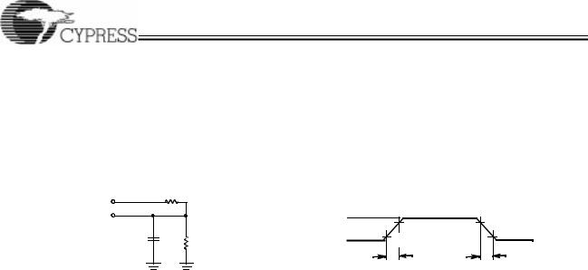
AC Test Loads and Waveforms[8, 9]
|
R11.1K Ω |
|
ALL INPUT PULSES |
||
5V |
|
|
|||
OUTPUT |
|
3.0V |
90% |
90% |
|
|
|
|
|||
|
|
|
10% |
||
CL |
R2 |
GND |
10% |
||
|
|||||
|
680Ω |
< 3 ns |
|
< 3 ns |
|
INCLUDING |
|
|
|||
|
|
|
|
||
JIG AND |
|
|
|
|
|
SCOPE |
42X5–4 |
|
|
42X5–5 |
|
Equivalent to: |
THÉEVENIN EQUIVALENT |
410Ω
OUTPUT


 1.91V
1.91V
Notes:
7.Tested initially and after any design or process changes that may affect these parameters.
8.CL = 30 pF for all AC parameters except for tOHZ.
9.CL = 5 pF for tOHZ.
Switching Characteristics Over the Operating Range
|
|
|
|
7C42X5-10 |
7C42X5-15 |
7C42X5-25 |
7C42X5-35 |
|
||||
|
|
|
|
|
|
|
|
|
|
|||
Parameter |
Description |
Min. |
Max. |
Min. |
Max. |
Min. |
Max. |
Min. |
Max. |
Unit |
||
|
|
|
|
|
|
|
|
|
|
|
||
tS |
Clock Cycle Frequency |
|
100 |
|
66.7 |
|
40 |
|
28.6 |
MHz |
||
tA |
Data Access Time |
2 |
8 |
2 |
10 |
2 |
15 |
2 |
20 |
ns |
||
tCLK |
Clock Cycle Time |
10 |
|
15 |
|
25 |
|
35 |
|
ns |
||
tCLKH |
Clock HIGH Time |
4.5 |
|
6 |
|
10 |
|
14 |
|
ns |
||
tCLKL |
Clock LOW Time |
4.5 |
|
6 |
|
10 |
|
14 |
|
ns |
||
tDS |
Data Set-Up Time |
3 |
|
4 |
|
6 |
|
7 |
|
ns |
||
tDH |
Data Hold Time |
0.5 |
|
1 |
|
1 |
|
2 |
|
ns |
||
tENS |
Enable Set-Up Time |
3 |
|
4 |
|
6 |
|
7 |
|
ns |
||
tENH |
Enable Hold Time |
0.5 |
|
1 |
|
1 |
|
2 |
|
ns |
||
tRS |
Reset Pulse Width[10] |
10 |
|
15 |
|
25 |
|
35 |
|
ns |
||
tRSR |
Reset Recovery Time |
8 |
|
10 |
|
15 |
|
20 |
|
ns |
||
tRSF |
Reset to Flag and Output Time |
|
10 |
|
15 |
|
25 |
|
35 |
ns |
||
tPRT |
Retransmit Pulse Width |
12 |
|
15 |
|
25 |
|
35 |
|
ns |
||
tRTR |
Retransmit Recovery Time |
12 |
|
15 |
|
25 |
|
35 |
|
ns |
||
tOLZ |
Output Enable to Output in Low Z[11] |
0 |
|
0 |
|
0 |
|
0 |
|
ns |
||
tOE |
Output Enable to Output Valid |
3 |
7 |
3 |
8 |
3 |
12 |
3 |
15 |
ns |
||
tOHZ |
Output Enable to Output in High Z[12] |
3 |
7 |
3 |
8 |
3 |
12 |
3 |
15 |
ns |
||
tWFF |
Write Clock to Full Flag |
|
8 |
|
10 |
|
15 |
|
20 |
ns |
||
tREF |
Read Clock to Empty Flag |
|
8 |
|
10 |
|
15 |
|
20 |
ns |
||
tPAFasynch |
Clock to Programmable Almost-Full Flag[12] |
|
12 |
|
16 |
|
20 |
|
25 |
ns |
||
|
(Asynchronous mode, VCC |
/SMODE |
tied to VCC) |
|
|
|
|
|
|
|
|
|
5
CY7C4425/4205/4215
CY7C4225/4235/4245
Switching Characteristics Over the Operating Range (continued)
|
|
|
|
|
|
7C42X5-10 |
7C42X5-15 |
7C42X5-25 |
7C42X5-35 |
|
||||
|
|
|
|
|
|
|
|
|
|
|||||
Parameter |
Description |
Min. |
Max. |
Min. |
Max. |
Min. |
Max. |
Min. |
Max. |
Unit |
||||
|
|
|
|
|
|
|
|
|
|
|
||||
tPAFsynch |
Clock to Programmable Almost-Full Flag |
|
8 |
|
10 |
|
15 |
|
20 |
ns |
||||
|
(Synchronous mode, VCC |
/SMODE |
tied to VSS) |
|
|
|
|
|
|
|
|
|
||
tPAEasynch |
Clock to Programmable Almost-Empty Flag[12] |
|
12 |
|
16 |
|
20 |
|
25 |
ns |
||||
|
(Asynchronous mode, VCC |
/SMODE |
tied to VCC) |
|
|
|
|
|
|
|
|
|
||
tPAEsynch |
Clock to Programmable Almost-Full Flag |
|
8 |
|
10 |
|
15 |
|
20 |
ns |
||||
|
(Synchronous mode, VCC |
/SMODE |
tied to VSS) |
|
|
|
|
|
|
|
|
|
||
tHF |
Clock to Half-Full Flag |
|
12 |
|
16 |
|
20 |
|
25 |
ns |
||||
tXO |
Clock to Expansion Out |
|
7 |
|
10 |
|
15 |
|
20 |
ns |
||||
tXI |
Expansion in Pulse Width |
3 |
|
6.5 |
|
10 |
|
14 |
|
ns |
||||
tXIS |
Expansion in Set-Up Time |
4.5 |
|
5 |
|
10 |
|
15 |
|
ns |
||||
tSKEW1 |
Skew Time between Read Clock and Write |
5 |
|
6 |
|
10 |
|
12 |
|
ns |
||||
|
Clock for Full Flag |
|
|
|
|
|
|
|
|
|
||||
|
|
|
|
|
|
|
|
|
|
|
||||
tSKEW2 |
Skew Time between Read Clock and Write |
5 |
|
6 |
|
10 |
|
12 |
|
ns |
||||
|
Clock for Empty Flag |
|
|
|
|
|
|
|
|
|
||||
|
|
|
|
|
|
|
|
|
|
|
||||
tSKEW3 |
Skew Time between Read Clock and Write |
10 |
|
15 |
|
18 |
|
20 |
|
ns |
||||
|
Clock for Programmable Almost Empty and Pro- |
|
|
|
|
|
|
|
|
|
||||
|
grammable Almost Full Flags. |
|
|
|
|
|
|
|
|
|
||||
|
|
|
|
|
|
|
|
|
|
|
|
|
|
|
Switching Waveforms
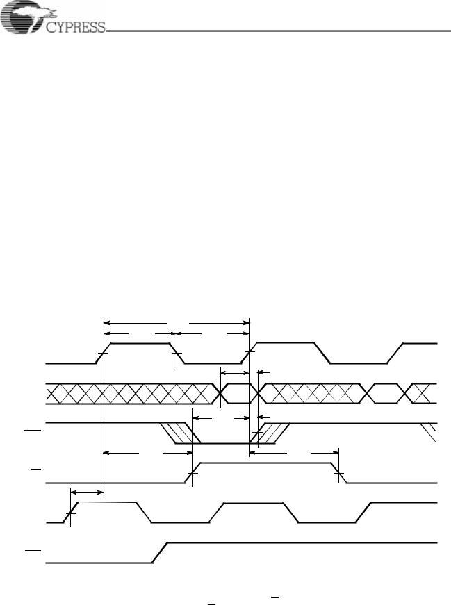
Write Cycle Timing |
|
|
|
tCLK |
|
tCLKH |
tCLKL |
|
WCLK |
|
|
|
tDS |
tDH |
D0 –D17 |
|
|
|
tENS |
tENH |
|
|
|
WEN |
|
NO OPERATION |
tWFF |
|
tWFF |
FF |
|
|
tSKEW1[13] |
|
|
RCLK
REN
42X5–6
Notes:
10.Pulse widths less than minimum values are not allowed.
11.Values guaranteed by design, not currently tested.
12.PAFasynch, tPAEasynch, after program register write will not be valid until 5 ns + tPAF(E).
13.tSKEW1 is the minimum time between a rising RCLK edge and a rising WCLK edge to guarantee that FF will go HIGH during the current clock cycle. If the time between the rising edge of RCLK and the rising edge of WCLK is less than tSKEW1, then FF may not change state until the next WCLK edge.
6

CY7C4425/4205/4215
CY7C4225/4235/4245
Switching Waveforms (continued) |
|
|
Read Cycle Timing |
|
|
|
|
tCLK |
|
tCLKH |
tCLKL |
RCLK |
|
|
tENS |
tENH |
|
REN |
|
NO OPERATION |
|
tREF |
tREF |
EF |
|
|
|
|
|
|
tA |
|
Q0 –Q17 |
|
VALID DATA |
|
tOLZ |
tOHZ |
|
tOE |
|
OE |
|
|
|
|
[14] |
|
|
tSKEW2 |
WCLK |
|
|
WEN
42X5–7
Reset Timing[15]
|
tRS |
|
RS |
|
tRSR |
REN, WEN, |
|
|
LD |
|
tRSF |
|
EF,PAE |
|
tRSF |
|
FF,PAF, |
|
HF |
|
tRSF |
|
OE=1[16] |
|
Q0 - Q17 |
|
OE=0 |
|
42X5–8 |
Notes: |
|
14. |
.tSKEW2 is the minimum time between a rising WCLK edge and a rising RCLK edge to guarantee that EF will go HIGH during the current clock cycle. It the time between the |
rising edge of WCLK and the rising edge of RCLK is less than tSKEW2, then EF may not change state until the next RCLK edge.
15.The clocks (RCLK, WCLK) can be free-running during reset.
16.After reset, the outputs will be LOW if OE = 0 and three-state if OE = 1.
7

CY7C4425/4205/4215
CY7C4225/4235/4245
Switching Waveforms (continued)
First Data Word Latency after Reset with Simultaneous Read and Write
WCLK |
|
|
|
|
|
|
tDS |
|
|
|
|
|
|
D0 –D17 |
D0 (FIRSTVALIDWRITE) |
D1 |
D2 |
|
D3 |
D4 |
tENS |
|
|
|
|
|
|
WEN |
|
[17] |
|
|
|
|
|
tFRL |
|
|
|
|
|
|
tSKEW2 |
|
|
|
|
|
RCLK |
|
|
|
|
|
|
|
|
tREF |
|
|
|
|
EF |
|
|
|
|
|
|
REN |
|
|
|
|
|
|
|
|
|
tA |
|
[18] |
|
|
|
|
|
tA |
|
|
Q0 –Q17 |
|
|
|
|
D |
D |
|
|
|
|
|
0 |
1 |
|
|
tOLZ |
tOE |
|
|
|
|
|
|
|
|
|
|
OE |
|
|
|
|
|
|
|
|
|
|
|
|
42X5–9 |
Empty Flag Timing |
|
|
|
|
|
|
WCLK |
|
|
|
|
|
|
tDS |
|
|
tDS |
|
|
|
D0 –D17 |
D0 |
|
|
D1 |
|
|
t |
tENH |
|
t |
tENH |
|
|
ENS |
|
|
ENS |
|
|
|
WEN |
|
|
|
|
|
|
|
[17] |
|
|
t |
[17] |
|
|
tFRL |
|
|
FRL |
|
|
RCLK |
|
|
|
|
|
|
|
t |
tREF |
t |
t |
|
t |
|
SKEW2 |
|
REF |
SKEW2 |
|
REF |
EF |
|
|
|
|
|
|
REN |
|
|
|
|
|
|
OE |
|
|
|
|
|
|
|
|
|
tA |
|
|
|
Q0 –Q17 |
|
|
|
|
|
D0 |
|
|
|
|
|
|
42X5–10 |
Notes:
17.When tSKEW2 > minimum specification, tFRL (maximum) = tCLK + tSKEW2. When tSKEW2 < minimum specification, tFRL (maximum) = either 2*tCLK + tSKEW2 or tCLK + tSKEW2. The Latency Timing applies only at the Empty Boundary (EF = LOW).
18.The first word is available the cycle after EF goes HIGH, always.
8
 Loading...