


 Loading...
Cypress Semiconductor CY7C1041BL-17ZC, CY7C1041BL-17VC, CY7C1041BL-15ZC, CY7C1041BL-15VC, CY7C1041B-25ZI Datasheet
...
CY7C1041B
Features
•High speed
—tAA = 12 ns
•Low active power
—1540 mW (max.)
•Low CMOS standby power (L version)
—2.75 mW (max.)
•2.0V Data Retention (400 W at 2.0V retention)
•Automatic power-down when deselected
•TTL-compatible inputs and outputs
•Easy memory expansion with CE and OE features
Functional Description
The CY7C1041B is a high-performance CMOS static RAM organized as 262,144 words by 16 bits.
Writing to the device is accomplished by taking Chip Enable (CE) and Write Enable (WE) inputs LOW. If Byte Low Enable (BLE) is LOW, then data from I/O pins (I/O0 through I/O7), is
256K x 16 Static RAM
written into the location specified on the address pins (A0 through A17). If Byte High Enable (BHE) is LOW, then data from I/O pins (I/O8 through I/O15) is written into the location specified on the address pins (A0 through A17).
Reading from the device is accomplished by taking Chip Enable (CE) and Output Enable (OE) LOW while forcing the Write Enable (WE) HIGH. If Byte Low Enable (BLE) is LOW, then data from the memory location specified by the address pins will appear on I/O0 to I/O7. If Byte High Enable (BHE) is LOW, then data from memory will appear on I/O8 to I/O15. See the truth table at the back of this data sheet for a complete description of read and write modes.
The input/output pins (I/O0 through I/O15) are placed in a high-impedance state when the device is deselected (CE HIGH), the outputs are disabled (OE HIGH), the BHE and BLE are disabled (BHE, BLE HIGH), or during a write operation (CE LOW, and WE LOW).
The CY7C1041B is available in a standard 44-pin 400-mil-wide body width SOJ and 44-pin TSOP II package with center power and ground (revolutionary) pinout.
Logic Block Diagram |
Pin Configuration |
A0  A1
A1  A2
A2 
A3  A4
A4 
A5  A6
A6 
A7  A8
A8 
ROW DECODER
INPUT BUFFER
|
|
256K x 16 |
|
|
AMPS |
I/O0 |
– I/O7 |
||
|
|
|
|
|
|||||
|
|
|
ARRAY |
|
|
SENSE |
|
|
|
|
|
1024 x 4096 |
|
I/O8 |
– I/O15 |
||||
|
|
|
|
||||||
|
|
|
|
|
|
|
|
||
|
|
COLUMN |
|
|
|
|
|
||
|
|
DECODER |
|
|
|
|
|
||
9 |
10 |
11 |
12 13 |
14 |
15 |
16 |
17 |
|
|
A A A A A A A A A |
|
BHE |
|||||||
|
|
|
|
|
|
|
|
|
|
|
|
|
|
|
|
|
|
|
WE |
|
|
|
|
|
|
|
|
|
CE |
|
|
|
|
|
|
|
|
|
OE |
|
|
|
|
|
|
|
|
|
BLE |
|
|
|
|
|
|
|
|
|
1041B–1 |
SOJ
TSOP II
Top View
|
A0 |
|
1 |
44 |
|
|
A17 |
|||
|
|
|
|
|||||||
|
|
|
||||||||
|
A1 |
|
2 |
43 |
|
|
A16 |
|||
|
|
|||||||||
|
A2 |
|
3 |
42 |
|
|
A15 |
|||
|
|
|
||||||||
|
A3 |
|
4 |
41 |
|
|
OE |
|
|
|
|
|
|||||||||
|
A4 |
|
5 |
40 |
|
|
BHE |
|||
|
|
39 |
|
|
||||||
|
CE |
|
|
6 |
|
|
BLE |
|||
|
|
|
||||||||
I/O0 |
|
7 |
38 |
|
|
I/O15 |
||||
|
|
|
||||||||
|
|
|
|
|||||||
I/O1 |
|
8 |
37 |
|
|
I/O14 |
||||
|
|
|
||||||||
I/O2 |
|
9 |
36 |
|
|
I/O13 |
||||
|
|
|
|
|
|
|
|
|
|
|
I/O3 |
|
10 |
35 |
|
|
I/O12 |
||||
|
|
|
||||||||
|
|
|
|
|||||||
VCC |
|
11 |
34 |
|
|
VSS |
||||
|
|
|
||||||||
VSS |
|
12 |
33 |
|
|
VCC |
||||
|
|
|
||||||||
I/O4 |
|
13 |
32 |
|
|
I/O11 |
||||
|
|
|||||||||
I/O5 |
|
14 |
31 |
|
|
I/O10 |
||||
|
|
|||||||||
I/O6 |
|
15 |
30 |
|
|
I/O9 |
||||
|
|
|||||||||
I/O7 |
|
16 |
29 |
|
|
I/O8 |
||||
|
|
|||||||||
WE |
|
17 |
28 |
|
NC |
|||||
|
A5 |
|
18 |
27 |
|
|
A14 |
|||
|
|
|||||||||
|
|
|||||||||
|
A6 |
|
19 |
26 |
|
|
A13 |
|||
|
|
|
|
|||||||
|
A7 |
|
20 |
25 |
|
|
A12 |
|||
|
|
|||||||||
|
A8 |
|
21 |
24 |
|
|
A11 |
|||
|
|
|
|
|||||||
|
A9 |
|
22 |
23 |
|
|
A10 |
|||
|
|
|||||||||
1041B–2
Selection Guide
|
|
|
|
7C1041B-12 |
7C1041B-15 |
7C1041B-17 |
|
7C1041B-20 |
7C1041B-25 |
|
|
|
|
|
|
|
|
|
|
|
|
Maximum Access Time (ns) |
|
|
|
12 |
15 |
|
17 |
|
20 |
25 |
|
|
|
|
|
|
|
|
|
|
|
Maximum Operating Current (mA) |
Com’l |
|
|
200 |
190 |
|
180 |
|
170 |
160 |
|
|
|
|
|
|
|
|
|
|
|
|
Ind’l |
|
|
220 |
210 |
|
200 |
|
190 |
180 |
|
|
|
|
|
|
|
|
|
|
|
Maximum CMOS Standby Current |
Com’l |
|
|
3 |
3 |
|
3 |
|
3 |
3 |
(mA) |
|
|
|
|
|
|
|
|
|
|
Com’l |
L |
|
- |
0.5 |
|
0.5 |
|
0.5 |
0.5 |
|
|
|
|
|
|||||||
|
|
|
|
|
|
|
|
|
|
|
|
Ind’l |
|
|
- |
6 |
|
6 |
|
6 |
6 |
|
|
|
|
|
|
|
|
|
|
|
Cypress Semiconductor Corporation • |
|
3901 North First Street • |
San Jose • |
CA 95134 • |
408-943-2600 |
|||||
|
|
|
|
|
|
|
|
|
|
March 23, 2001 |

CY7C1041B
Maximum Ratings
(Above which the useful life may be impaired. For user guidelines, not tested.)
Storage Temperature –65° C to +150° C
Ambient Temperature with Power Applied–55° C to +125° C
Supply Voltage on VCC to Relative GND[1]–0.5V to +7.0V
DC Voltage Applied to Outputs
in High Z State[1]–0.5V to VCC + 0.5V
Electrical Characteristics Over the Operating Range
DC Input Voltage[1]–0.5V to VCC + 0.5V
Current into Outputs (LOW)20 mA
Operating Range
|
Ambient |
|
Range |
Temperature[2] |
VCC |
Commercial |
0° C to +70° C |
5V ± 0.5 |
|
|
|
Industrial |
–40° C to +85° C |
|
|
|
|
|
|
|
|
|
|
|
|
7C1041B-12 |
7C1041B-15 |
7C1041B-17 |
|
|||
|
|
|
|
|
|
|
|
|
|
|
|
|||
Parameter |
Description |
Test Conditions |
|
|
Min. |
Max. |
Min. |
Max. |
Min. |
Max. |
Unit |
|||
|
|
|
|
|
|
|
|
|
|
|
|
|||
VOH |
Output HIGH Voltage |
VCC = Min., IOH = –4.0 mA |
|
|
2.4 |
|
2.4 |
|
2.4 |
|
V |
|||
VOL |
Output LOW Voltage |
VCC = Min., IOL = 8.0 mA |
|
|
|
0.4 |
|
0.4 |
|
0.4 |
V |
|||
VIH |
Input HIGH Voltage |
|
|
|
|
|
|
2.2 |
VCC |
2.2 |
VCC |
2.2 |
VCC |
V |
|
|
|
|
|
|
|
|
|
+ 0.5 |
|
+ 0.5 |
|
+ 0.5 |
|
|
|
|
|
|
|
|
|
|
|
|
|
|
|
|
VIL |
Input LOW Voltage[1] |
|
|
|
|
|
|
–0.5 |
0.8 |
–0.5 |
0.8 |
–0.5 |
0.8 |
V |
IIX |
Input Load Current |
GND < VI < VCC |
|
|
|
–1 |
+1 |
–1 |
+1 |
–1 |
+1 |
A |
||
IOZ |
Output Leakage |
GND < VOUT < VCC, |
|
|
|
–1 |
+1 |
–1 |
+1 |
–1 |
+1 |
A |
||
|
Current |
Output Disabled |
|
|
|
|
|
|
|
|
|
|
||
|
|
|
|
|
|
|
|
|
|
|
|
|
||
ICC |
VCC Operating |
VCC = Max., |
Com’l |
|
|
|
200 |
|
190 |
|
180 |
mA |
||
|
Supply Current |
f = fMAX = 1/tRC |
|
|
|
|
|
|
|
|
|
|
||
|
Ind’l |
|
|
|
220 |
|
210 |
|
200 |
mA |
||||
|
|
|
|
|
|
|
|
|
|
|
|
|
|
|
ISB1 |
Automatic CE |
Max. VCC, |
|
> VIH |
|
|
|
|
40 |
|
40 |
|
40 |
mA |
CE |
|
|
|
|
|
|
||||||||
|
Power-Down Current |
VIN > VIH or |
|
|
|
|
|
|
|
|
|
|
||
|
—TTL Inputs |
VIN < VIL, f = fMAX |
|
|
|
|
|
|
|
|
|
|
||
ISB2 |
Automatic CE |
Max. VCC, |
Com’l |
|
|
|
3 |
|
3 |
|
3 |
mA |
||
|
Power-Down Current |
CE > VCC – 0.3V, |
|
|
|
|
|
|
|
|
|
|
||
|
Com’l |
L |
|
- |
|
0.5 |
|
0.5 |
mA |
|||||
|
—CMOS Inputs |
VIN > VCC – 0.3V, |
|
|
|
|
|
|
|
|
|
|
||
|
|
|
|
|
|
|
|
|
|
|
||||
|
|
or VIN < 0.3V, f = 0 |
Ind’l |
|
|
|
- |
|
6 |
|
6 |
mA |
||
Notes:
1.VIL (min.) = –2.0V for pulse durations of less than 20 ns.
2.TA is the case temperature.
2
CY7C1041B
Electrical Characteristics Over the Operating Range (continued)
|
|
Test Conditions |
|
|
7C1041B-20 |
7C1041B-25 |
|
|||||
|
|
|
|
|
|
|
|
|
|
|
|
|
Parameter |
Description |
|
|
|
|
|
|
Min. |
Max. |
Min. |
Max. |
Unit |
|
|
|
|
|
|
|
|
|
|
|||
VOH |
Output HIGH Voltage |
VCC = Min., IOH = –4.0 mA |
|
|
2.4 |
|
2.4 |
|
V |
|||
VOL |
Output LOW Voltage |
VCC = Min., IOL = 8.0 mA |
|
|
|
0.4 |
|
0.4 |
V |
|||
VIH |
Input HIGH Voltage |
|
|
|
|
|
|
2.2 |
VCC |
2.2 |
VCC + 0.5 |
V |
|
|
|
|
|
|
|
|
|
+ 0.5 |
|
|
|
|
|
|
|
|
|
|
|
|
|
|
|
|
VIL |
Input LOW Voltage[1] |
|
|
|
|
|
|
–0.5 |
0.8 |
–0.5 |
0.8 |
V |
IIX |
Input Load Current |
GND < VI < VCC |
|
|
|
–1 |
+1 |
–1 |
+1 |
A |
||
IOZ |
Output Leakage |
GND < VOUT < VCC, |
|
|
|
–1 |
+1 |
–1 |
+1 |
A |
||
|
Current |
Output Disabled |
|
|
|
|
|
|
|
|
||
|
|
|
|
|
|
|
|
|
|
|
||
ICC |
VCC Operating |
VCC = Max., |
Com’l |
|
|
|
170 |
|
160 |
mA |
||
|
Supply Current |
f = fMAX = 1/tRC |
|
|
|
|
|
|
|
|
||
|
Ind’l |
|
|
|
190 |
|
180 |
mA |
||||
ISB1 |
Automatic CE |
Max. VCC, |
|
> VIH |
|
|
|
|
40 |
|
40 |
mA |
CE |
|
|
|
|
|
|||||||
|
Power-Down Current |
VIN > VIH or |
|
|
|
|
|
|
|
|
||
|
—TTL Inputs |
VIN < VIL, f = fMAX |
|
|
|
|
|
|
|
|
||
ISB2 |
Automatic CE |
Max. VCC, |
Com’l |
|
|
|
3 |
|
3 |
mA |
||
|
Power-Down Current |
CE > VCC – 0.3V, |
|
|
|
|
|
|
|
|
||
|
Com’l |
L |
|
0.5 |
|
0.5 |
mA |
|||||
|
—CMOS Inputs |
VIN > VCC – 0.3V, |
|
|
|
|
|
|
|
|
||
|
Ind’l |
|
|
|
6 |
|
6 |
mA |
||||
|
|
or VIN < 0.3V, f = 0 |
|
|
|
|
||||||
Capacitance[3]
Parameter |
Description |
Test Conditions |
Max. |
Unit |
|
|
|
|
|
|
|
CIN |
Input Capacitance |
TA = 25° C, f = 1 MHz, |
8 |
pF |
|
|
|
VCC = 5.0V |
|
|
|
COUT |
I/O Capacitance |
8 |
pF |
||
|
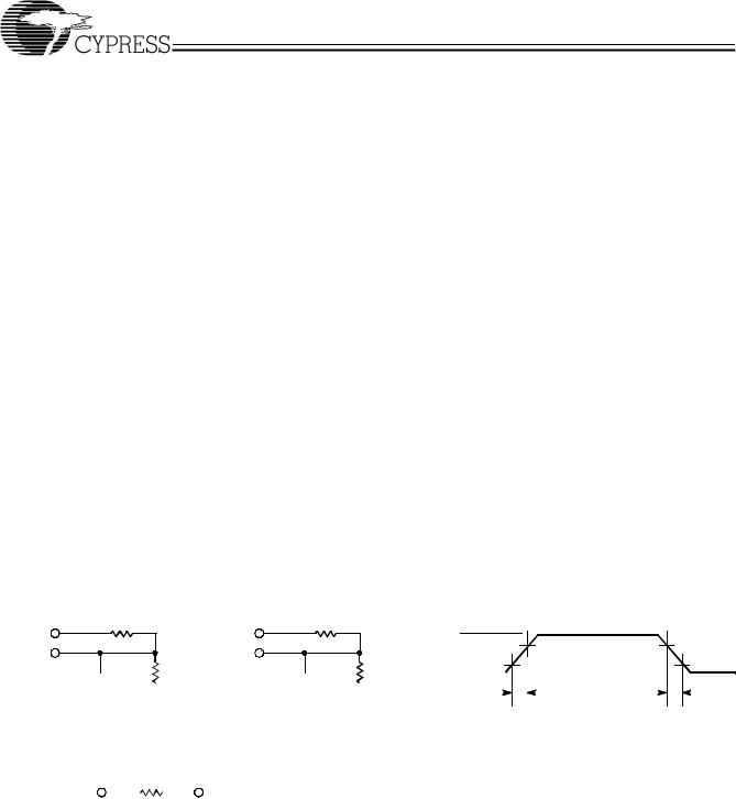
AC Test Loads and Waveforms |
|
|
||
R1 481Ω |
R1 481Ω |
ALL INPUT PULSES |
|
|
5V |
5V |
3.0V |
|
|
OUTPUT |
OUTPUT |
90% |
90% |
|
10% |
10% |
|||
|
|
|||
30 pF |
|
|
|
|
|
|
|
|
|
|
|
|
|
|
R2 |
5 pF |
|
|
|
|
|
|
|
|
|
|
|
|
|
R2 |
GND |
|
|
|
|
|
|
|
|
|
|
|
INCLUDING |
|
|
|
|
|
|
|
|
|
|
|
|
|
|
255Ω |
INCLUDING |
|
|
|
|
|
|
|
|
|
|
|
|
|
|
255Ω |
≤ 3 ns |
|
|
|
|
|
|
|
|
≤ 3 ns |
|
|
|
|
|
|
|
|
|
|
|
|
|
|
|
|
|
|
|
|
|
|
|
|
|
|
|
|
|
|
|
|||||||||||||
|
|
|
|
|
|
|
|
|
|
|
|
|
|
|
|
|
|
|
|
|
|
|
|
|
|
|
|
|
|
|
|
|
|
|
|
|
|
|||||
|
|
|
|
|
|
|
|
|
|
|
|
|
|
|
|
|
|
|
|
|
|
|
|
|
|
|
|
|
|
|
|
|
|
|
|
|
|
|
|
|
||
|
|
|
|
|
|
|
|
|
|
|
|
|
|
|
|
|
|
|
|
|
|
|
|
|
|
|
|
|
|
|
|
|
|
|
|
|
|
|
|
|||
JIG AND |
|
|
|
|
|
|
|
|
|
|
|
|
|
|
|
JIG AND |
|
|
|
|
|
|
|
|
|
|
|
|
|
|
|
|
|
|
|
|
|
|
|
|
|
|
SCOPE |
(a) |
SCOPE |
(b) |
1041B–3 |
|
|
|
|
|
|
|
|
|
|
|
|||||||||||||||||||||||||||
|
|
|
|
|
|
|
|
|
|
|
|
|
|
|
|
|
|
|
|
|
|
|
|
|
|
|
|
|
|
|
|
|
|
|
|
|
|
|
|
|
|
1041B–4 |
Equivalent to: THÉ VENIN EQUIVALENT |
|
|
|
|
|
|
|
|
|
|
|
|
|
|
|
|
|
|
|
|
|
|
|
|
|
|||||||||||||||||
OUTPUT |
|
|
167Ω |
1.73V |
|
|
|
|
|
|
|
|
|
|
|
|
|
|
|
|
|
|
|
|
|
|
|
|
|
|||||||||||||
|
|
|
|
|
|
|
|
|
|
|
|
|
|
|
|
|
|
|
|
|
|
|
|
|
|
|
|
|||||||||||||||
Note:
3.Tested initially and after any design or process changes that may affect these parameters.
3
Loading...