


CY7C4421-15JC
Cypress Semiconductor CY7C4421-15JC, CY7C4421-15AC, CY7C4421-10JC, CY7C4421-10AC, CY7C4421-25JCT Datasheet
...
32K x 16 Static RAM
CY7C1020
Cypress Semiconductor Corporation
• 3901 North First Street • San Jose • CA 95134 • 408-943-2600
October 18, 1999
7C10
Features
• 5.0V operation (± 10%)
• High speed
—t
AA
= 10 ns
• Low active power
—825 mW (max., 10 ns, “L” version)
• Very L ow standb y p ow e r
—550 µW (max., “L” version)
• Automat ic power-down when deselected
• Independent Control of Upper and Lower bytes
• Available in 44-pin TSOP II and 400-mil SOJ
Functional Description
The CY7C1020 is a high-performance CMOS static RAM organized as 32,768 words by 16 bits. This device has an automatic power-down feature that significantly reduces power
consumption when deselected.
Writing to the device is accomplished by taking Chip Enable
(CE
) and Write Enable (WE) inputs LOW. If Byte Low Enable
(BLE
) is LOW, then data from I/O pins (I/O1 through I/O8), is
written into the location specified on the address pins (A
0
through A14). If Byte High Enable (BHE) is LOW, then data
from I/O pins (I/O
9
through I/O16) is written into the location
specified on the address pins (A
0
through A14).
Reading from the device is accomplished by taking Chip Enable (CE
) and Output Enable (O E) LOW whil e for cing the Write
Enable (WE
) HIGH. If Byte Low Enable (BLE) is LOW, then
data from the memory location specified by the address pins
will appear on I /O
1
to I/O8. If Byte High Enable (BHE) is LOW ,
then data from memory will appear on I/O
9
to I/O16. See the
truth table a t the bac k of this dat a sheet f or a c omplete des cription of read and write modes.
The input/output pins (I/O
1
through I/O16) are placed in a
high-impedance state when the device is deselected (CE
HIGH), the outputs are disab led (OE HIGH ), the BHE and BLE
are disabl ed (BHE, BLE HIGH), or during a write oper ation (CE
LOW, and WE LOW).
The CY7C1020 is available in standard 44-pin TSOP type II
and 400-mil-wide SOJ packages.
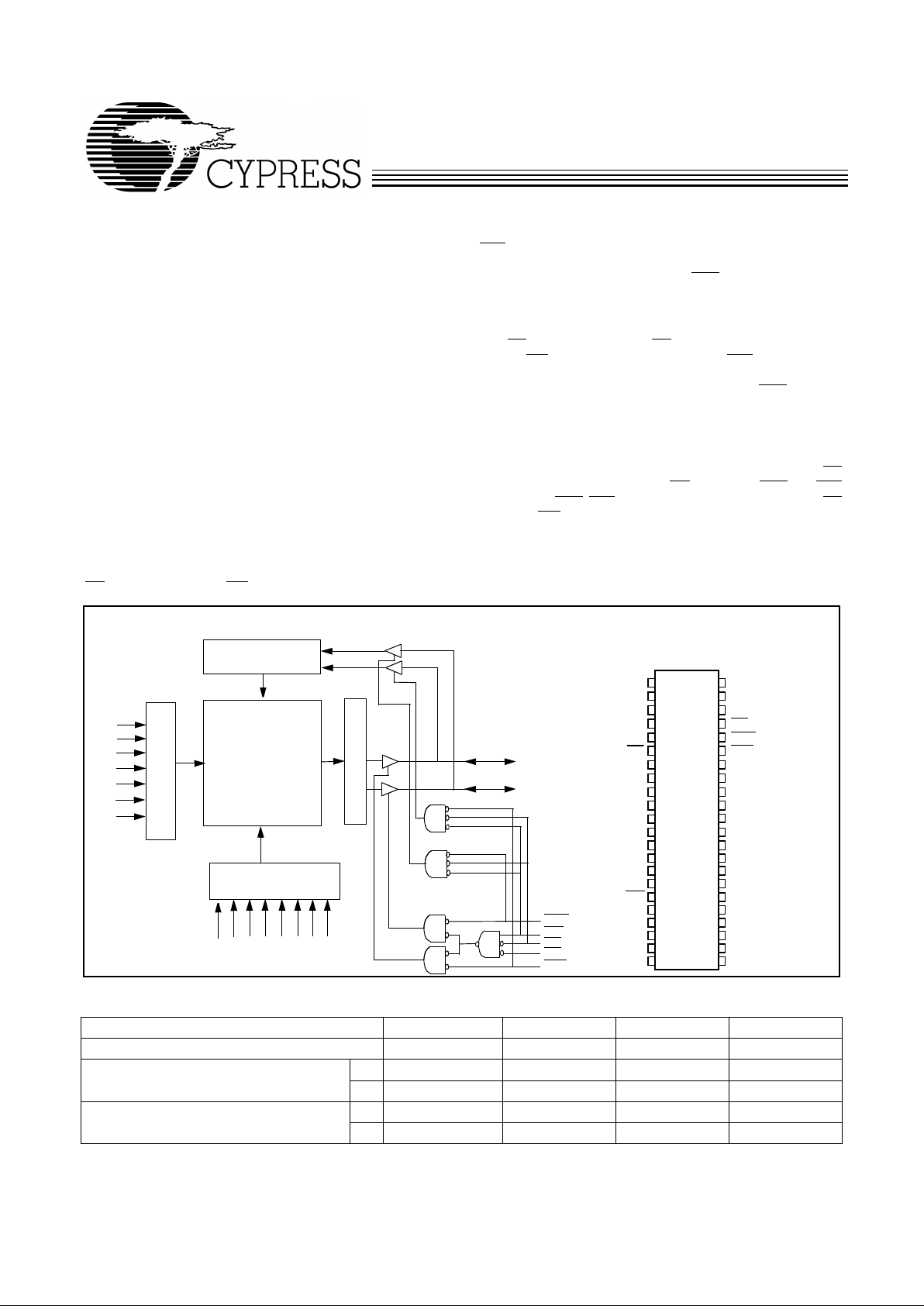
WE
Logic Block Diagram
Pin Configuration
1
2
3
4
5
6
7
8
9
10
11
14
31
32
36
35
34
33
37
40
39
38
Top View
SOJ / TSOP II
12
13
41
44
43
42
16
15
29
30
V
CC
A
10
A
9
A
8
A
7
NC
NC
A
14
OE
V
SS
A
0
I/O
16
A
13
CE
I/O
3
I/O
1
I/O
2
BHE
NC
A
12
A
11
1020-2
18
17
20
19
I/O
4
27
28
25
26
22
21
23
24
NC
V
SS
I/O
7
I/O
5
I/O
6
I/O
8
A
1
A
2
BLE
V
CC
I/O
15
I/O
14
I/O
13
I/O
12
I/O
11
I/O
10
I/O
9
A
3
A
4
A
5
A
6
32K x 16
RAM Array
I/O
1
– I/O
8
ROW DECODER
A
6
A
5
A
4
A
3
A
0
COLUMN DECODER
A
9
A10A11A12A13A
14
SENSE AMPS
DATA IN DRIVERS
OE
A
2
A
1
I/O9 – I/O
16
CE
WE
BLE
BHE
A
8
A
7
1020-1
Selection Guide
7C1020-10 7C1020-12 7C1020-15 7C1020-20
Maximum Access Time (ns) 10 12 15 20
Maximum Operating Curr ent (mA) 180 170 160 160
L150 140 130 130
Maximum CMOS Standby Current (mA) 3 3 3 3
L 0.1 0.1 0.1 0.1
CY7C1020
2
Maximum Ratings
(Above which the useful lif e m ay be impaired. For user guidelines, not tested.)
Storage Temperature .................................–65°C to +15 0°C
Ambient Temperature with
Power Applied.............................................–55°C to +125°C
Supply Voltage on V
CC
to Relative GND
[1]
....–0.5V to +7.0V
DC V oltage Applied to Outputs
in High Z State
[1]
.....................................–0.5V to VCC +0.5V
DC Input Voltage
[1]
..................................–0.5V to VCC +0.5V
Curre n t in to Out p ut s (L OW )........ .. .. .......... ... ......... ... .... 20 mA
Static Discharge Voltage .......... ......................... .. ......>2001V
(per MIL-STD-883, Method 3015)
Latch-Up Current.....................................................>200 mA
Operating Range
Range
Ambient
Temperature
[2]
V
CC
Commercial 0°C to +70°C 4.5V–5.5V
Electrical Characteristics
Over the Operating Range
Parameter Description Tes t Condi ti ons
7C1020-10
7C1020-12 7C1020-15
UnitMin. Max. Min. Ma x. Min. Max.
V
OH
Output HIGH Voltage VCC = Min., IOH = –4.0 mA 2. 4 2.4 2.4 V
V
OL
Output LOW Voltage VCC = Min., IOL = 8.0 mA 0.4 0.4 0.4 V
V
IH
Input HIGH Voltage 2.2 6.0 2.2 6.0 2.2 6.0 V
V
IL
Input LOW Voltage
[1]
–0.5 0.8 –0.5 0.8 –0.5 0.8 V
I
IX
Input Load Current GND < VI < V
CC
–1+1–1 +1 –1 +1
µA
I
OZ
Output Leakage
Current
GND < VI < VCC,
Output Disabled
–2+2–2 +2 –2 +2
µA
I
CC
VCC Operating
Supply Current
VCC = Max.,
I
OUT
= 0 mA,
f = f
MAX
= 1/t
RC
180 170 160 mA
L 150 140 130
I
SB1
Automatic CE
Power-Down Current
—TTL Inputs
Max. VCC, CE > V
IH
VIN > VIH or
V
IN
< VIL, f = f
MAX
20 20 20 mA
L1010 10
I
SB2
Automatic CE
Power-Down Current
—CMOS Inputs
Max. VCC,
CE
> VCC – 0.3V,
V
IN
> VCC – 0.3V,
or V
IN
< 0.3V, f = 0
3 3 3 mA
L 100 100 100 µA
Notes:
1. V
IL
(min.) = –2.0V for pulse durations of les s tha n 20 n s.
2. T
A
is the case tempe ra ture.
CY7C1020
3
Electrical Characteristics
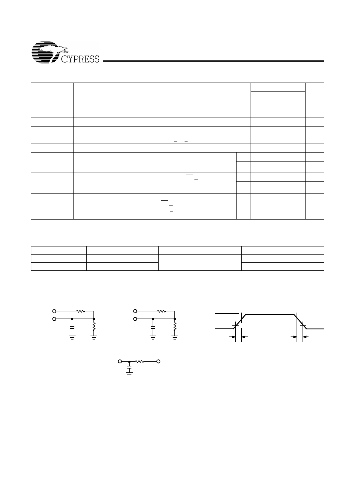
Over the Operating Range (continued)
Parameter Description Te st Condi tions
7C1020-20
UnitMin. Max.
V
OH
Outp ut HIGH Voltage VCC = Min. , IOH = –4.0 mA 2.4 V
V
OL
Output LOW Voltage VCC = Min. , IOL = 8.0 mA 0.4 V
V
IH
Input HIGH Voltage 2.2 6.0 V
V
IL
Input LOW Voltage
[1]
–0.5 0.8 V
I
IX
Input Load Current GND < VI < V
CC
–1+1µA
I
OZ
Output Leakage Current GND < VI < VCC, Output Disabled –2+2µA
I
CC
VCC Operating
Supply Current
VCC = Max .,
I
OUT
= 0 mA,
f = f
MAX
= 1/t
RC
160 mA
L 130
I
SB1
Automatic CE
Power-Down Current
—TTL Inputs
Max. VCC, CE > V
IH
VIN > VIH or
V
IN
< VIL, f = f
MAX
20 mA
L10
I
SB2
Automatic CE
Power-Down Current
—CMOS Inputs
Max. V
CC
,
CE
> VCC – 0.3V,
V
IN
> VCC – 0.3V,
or V
IN
< 0.3V, f = 0
3mA
L 100 µA
Capacitance
[3]
Parameter Description Te st Condi tions Max. Unit
C
IN
Input Capacitance TA = 25°C, f = 1 MHz,
V
CC
= 5.0V
8 pF
C
OUT
Output Capacitance 8 pF
Note:
3. Tested initially and after any design or process changes that may affect these parameters.
AC Test Loads and Waveforms
1020-3
1020-4
90%
10%
3.0V
GND
90%
10%
ALL INPUT PULSES
5V
OUTPUT
30 pF
INCLUDING
JIG AND
SCOPE
5V
OUTPUT
5 pF
INCLUDING
JIG AND
SCOPE
(a)
(b)
<3 ns <3 ns
OUTPUT
R 481
Ω
R 481
Ω
R2
255
Ω
R2
255
Ω
167
Ω
Equivalent to:
THÉVENIN
EQUIVALENT
1.73V
30 pF
 Loading...