

Page 1
Clarion Co., Ltd.
P
O
W
E
R
D
I
S
C
U
P
STOP MUTE
123456
T
O
P
TILTM.L
ADJ A-MLIST
KEY P AD
MENU
LOUDDV TI T LE MONISTOPDV SETUP
50 Kamitoda, Toda-shi, Saitama 335-8511 Japan
Service Dept.: 5-66 Azuma , Kitamoto-shi, Saitama 364-0007 Japan
Tel: +81-48-541-2335 / 2432 FAX: +81-48-541-2703
Service Manual
Published by Service Dept.
298-6047-00
Printed in Japan
Jan.2003 P
R
R
AM/FM MAIN
RADIO ANT
CCD
VISUAL2 IN
AUDIO OUT
FRONTNON-FADER
REAR
LINE I N LINE OUT
R
ORIGINAL SERVICE MANUAL
This additional service manual is designed to be used together with Model VRX925VD.
Original model Manual No.
VRX925VD 298-5995-00
DIFFERENCE FROM ORIGINAL
SERVICE MANUAL
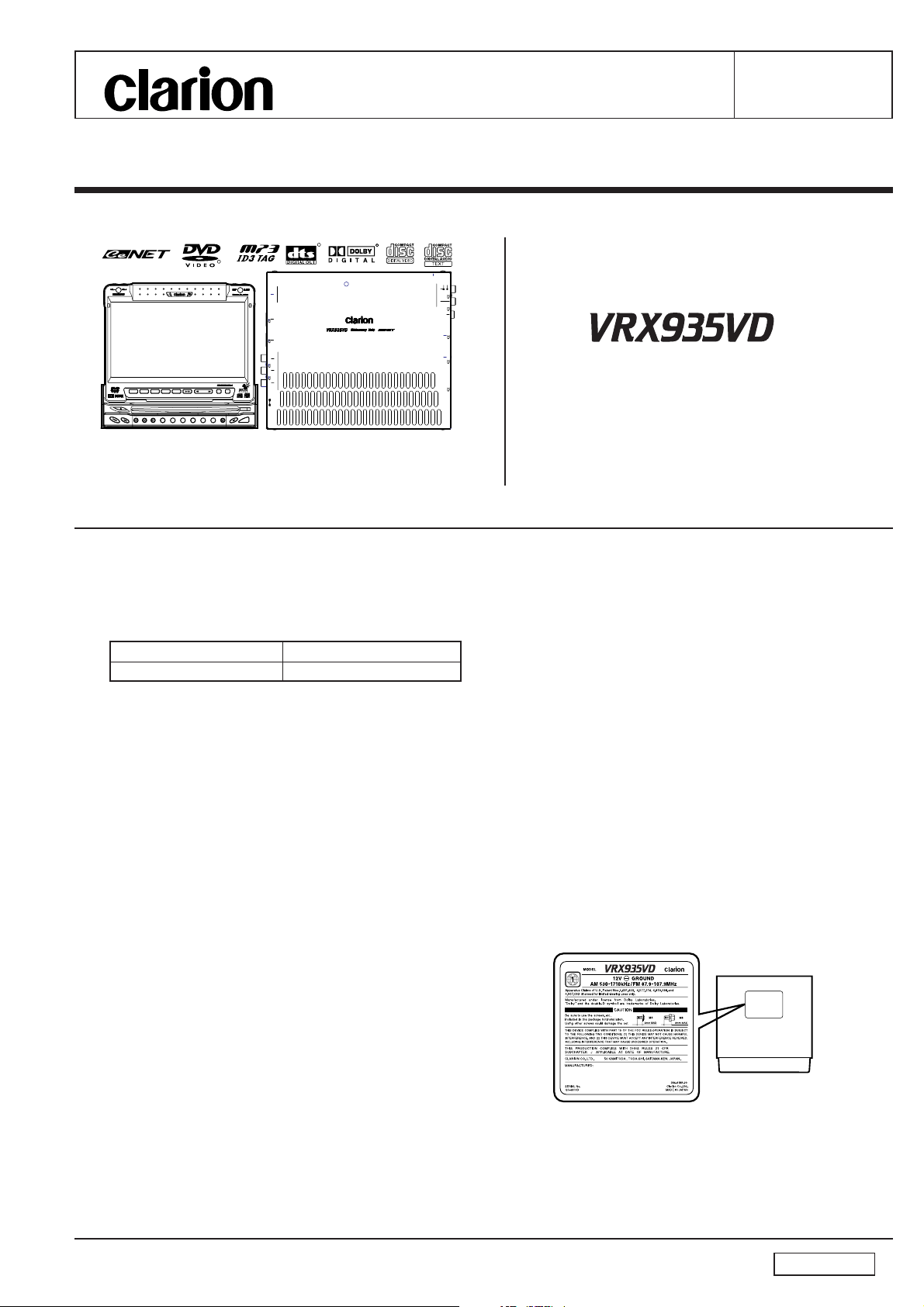
1. Model name(VRX935VD)
2. Design change(panel/buttons)
3. Display control IC/ ROM IC
DVD mechanism control IC
COMPONENTS
QC-6810B-C/QC-6810K-D/K-E
Main unit ----------- 1
Remote control unit RCB-161-600 1
Battery(SUM-3) ----------- 2
Universal mounting bracket 300-9035-01 1
DCP case 335-6707-00 1
Antenna jumper 093-1465-03 1
Power supply lead(18P) 854-6392-50 1
Power supply lead(2P) 854-6393-51 1
Extension lead(20P to 20P) 855-0553-00 1
Outer escutcheon 940-7715-07 1
Parts bag -----------
Electro tap 060-0018-00 1
Machine screw(M4x3) 714-4003-87 4
Machine screw(M5x8) 714-5008-41 4
Sems hex. bolt(M5x8) 716-0496-01 5
AM/FM DVD Video/Video CD/CD/
RESET
TV-TUNER
(DVD A/C)
VIDEO
VISUAL1 IN
AUDIO
VIDEO OUT
MAINUNIT
Ce-NET
MP3 Player/CD Changer Controller
with 7" LC Display
Model
(QC-6810B-C)
(for U.S.A./ Region No. "1")
(QC-6810K-D)
(for ASIA / Region No. "3")
(QC-6810K-E)
(for OCEANIA / Region No. "4")
Parts bag -----------
Hook plate 330-8216-01 2
Cord clamp 335-0833-01 1
Spacer 345-3653-01 1
Screw 716-0726-01 1
Parts bag -----------
Mounting bracket 300-7362-00 2
Canoe clip 335-2515-00 4
Machine screw(M4x8) 714-4008-80 4
Parts bag -----------
DCP lock spacer 345-5174-00 1
CAUTIONS
Use of controls,adjustment or performance of procedures
other than those specified herein,may result in hazardous
radiation exposure.
The COMPACT DISC player and MINI DISC player should
not be adjusted or repaired by anyone except properly qualified service personnel.
- 1 -
VRX935VD
Page 2

To engineers in charge of repair or
inspection of our products.
Before repair or inspection, make sure to follow the
instructions so that customers and Engineers in
charge of repair or inspection can avoid suffering
any risk or injury.
1. Use specified parts.
The system uses parts with special safety features against
fire and voltage. Use only parts with equivalent characteristics when replacing them.
The use of unspecified parts shall be regarded as remodeling for which we shall not be liable. The onus of product
liability (PL) shall not be our responsibility in cases where
an accident or failure is as a result of unspecified parts
being used.
2. Place the parts and wiring back in their original positions
after replacement or re-wiring.
For proper circuit construction, use of insulation tubes,
bonding, gaps to PWB, etc, is involved. The wiring connection and routing to the PWB are specially planned using clamps to keep away from heated and high voltage
parts. Ensure that they are placed back in their original
positions after repair or inspection.
If extended damage is caused due to negligence during
repair, the legal responsibility shall be with the repairing
company.
3. Check for safety after repair.
Check that the screws, parts and wires are put back securely in their original position after repair. Ensure for safety
reasons there is no possibility of secondary ploblems
around the repaired spots.
If extended damage is caused due to negligence of repair,
the legal responsibility shall be with the repairing company.
4. Caution in removal and making wiring connection to the
parts for the automobile.
Disconnect the battery terminal after turning the ignition
key off. If wrong wiring connections are made with the battery connected, a short circuit and/or fire may occur. If extensive damage is caused due to negligence of repair, the
legal responsibility shall be with the repairing company.
5. Cautions regarding chips.
Do not reuse removed chips even when no abnormality is
observed in their appearance. Always replace them with
new ones. (The chip parts include resistors, capacitors,
diodes, transistors, etc). The negative pole of tantalum
capacitors is highly susceptible to heat, so use special care
when replacing them and check the operation afterwards.
6. Cautions in handling flexible PWB
Before working with a soldering iron, make sure that the
iron tip temperature is around 270
ply the iron tip repeatedly(more than three times)to the
same patterns. Also take care not to apply the tip with force.
7. Turn the unit OFF during disassembly and parts replacement. Recheck all work before you apply power to the unit.
8. Cautions in checking that the optical pickup lights up.
The laser is focused on the disc reflection surface through
the lens of the optical pickup. When checking that the laser optical diode lights up, keep your eyes more than 30cms
away from the lens. Prolonged viewing of the laser within
30cms may damage your eyesight.
. Take care not to ap-
9. Cautions in handling the optical pickup
The laser diode of the optical pickup can be damaged by
electrostatic charge caused by your clothes and body. Make
sure to avoid electrostatic charges on your clothes or body,
or discharge static electricity before handling the optical
pickup.
9-1. Laser diode
The laser diode terminals are shorted for transportation in order to prevent electrostatic damage. After
replacement, open the shorted circuit. When removing the pickup from the mechanism, short the terminals by soldering them to prevent this damage.
9-2. Actuator
The actuator has a powerful magnetic circuit. If a
magnetic material is put close to it. Its characteristics will change. Ensure that no foreign substances
enter through the ventilation slots in the cover.
9-3. Cleaning the lens
Dust on the optical lens affects performance. To
clean the lens, apply a small amount of isopropyl
alcohol to lens paper and wipe the lens gently.
EXPLANATION OF IC
052-5041-53 TMP95CW64F-4N56(Z) DVD Mechanism Control-
1.Terminal Description
pin 1: A Vref : IN: Reference voltage for the internal ADC.
pin 2: A VSS : - : Analog ground.
pin 3:A VCC : - : Positive supply voltage for the internal
pin 4: NU : - : Not in use.
pin 5: NU : - : Not in use.
pin 6: Connect 7 : IN : Connect to pin7.
pin 7: EJECT SW : IN : Eject switch signal input.
pin 8: A MUTE : O : The audio mute signal output.
pin 9: SYS P 1 : O : System power 1 control signal output.
pin 10: NU : - : Not in use.
pin 11: RESET : O : Reset signal output.
pin 12: TEST 0 : O : For the test.
pin 13: TEST 1 : O : For the test.
pin 14: TEST 2 : O : For the test.
pin 15: TEST 3 : O : For the test.
pin 16: MCW : O : Loading motor control output.
pin 17: MCCW : O : Loading motor control output.
pin 18: TX D2 : O : The serial data output.
pin 19: RX D2 : IN: The serial data input.
pin 20: DVD R DE CS : O : The chip select signal output to the DVD
pin 21: DVD PRO CS : O : The chip enable signal output to DVD
pin 22: NU : - : Not in use.
pin 23: SPNDL CNT : O : Spindle control output.
pin 24: NU : - : Not in use.
pin 25: VCC : - : Positive supply voltage.
pin 26: GND : - : Ground.
pin 27: X 1 : - : Crystal connection.
pin 28: X 2 : - : Crystal connection.
pin 29: CNNCT VCC : IN: Connect to VCC.
pin 30: RESET : IN : Reset signal input.
pin 31: ACC CNT : IN: ACC ON signal input.
pin 32: NU : - : Not in use.
pin 33: LE TIME : O : For loading/eject time.
pin 34: FG PULSE : IN : FG pulse input.
pin 35: DISC MT SHRT : IN : Disc motor short brake.
pin 36: DATA REQ : O : The data request.
pin 37: D PRO INT : IN: The interrupt signal input from DVD pro-
pin 38: CMMD DT REQ : O : The command data request output.
analog section.
ROM decoder.
processor.
cessor.
ler
- 2 -VRX935VD
Page 3

pin 39: REM 5V : O : Power ON signal output to the 5V supply
pin 40: ID CONTINUE : O : ID check.
pin 41: DVD R DE INT : IN : The interrupt signal input from the DVD
pin 42: NU : - : Not in use.
pin 43: DVD R DE RST: O : The reset signal output to the DVD ROM
pin 44: VCC : - : Positive supply voltage.
pin 45: D 0 :I/O: Data input/output.
pin 46: D 1 :I/O: Data input/output.
pin 47: D 2 :I/O: Data input/output.
pin 48: D 3 :I/O: Data input/output.
pin 49: D 4 :I/O: Data input/output.
pin 50: D 5 :I/O: Data input/output.
pin 51: D 6 :I/O: Data input/output.
pin 52: D 7 :I/O: Data input/output.
pin 53: TEST 4 : O : For the test.
pin 54: TEST 5 : O : For the test.
pin 55: TEST 6 : O : For the test.
pin 56: TEST 7 : O : For the test.
pin 57: TEST 8 :I/O: For the test.
pin 58: TEST 9 :I/O: For the test.
pin 59: TEST 10 :I/O: For the test.
pin 60: TEST 11 :I/O: For the test.
pin 61: CNNCT VCC : IN: Connect to VCC.
pin 62: GN D : - : Ground.
pin 63: VCC : - : Positive supply voltage.
pin 64: BUSY OUT : O : Busy flag output.
pin 65: DISC :O : Disc distinction signal output.
pin 66: LAYER : O : Layer distinction signal output.
pin 67: NU : - : Not in use.
pin 68: CHUKING :IN : The chucking switch signal input.
pin 69: DVD MCH S 1 :IN : The sensor signal input from DVD mech-
pin 70: DVD MCH S 2 :IN : The sensor signal input from DVD mech-
pin 71: DVD MCH S 3 :IN : The sensor signal input from DVD mech-
pin 72: NU : - : Not in use.
pin 73: NU : - : Not in use.
pin 74: NU : - : Not in use.
pin 75: NU : - : Not in use.
pin 76: MA : O : MA.
pin 77: NU : - : Not in use.
pin 78: NU : - : Not in use.
pin 79: NU : - : Not in use.
pin 80: A D 7 : O : Address output.
pin 81: A D 6 : O : Address output.
pin 82: A D 5 : O : Address output.
pin 83: A D 4 : O : Address output.
pin 84: A D 3 : O : Address output.
pin 85: A D 2 : O : Address output.
pin 86: A D 1 : O : Address output.
pin 87: A D 0 : O : Address output.
pin 88: RD STRB : O : The read strobe output.
pin 89: WR STRB : O : The write strobe output.
pin 90: NU : - : Not in use.
pin 91: GN D : - : Ground.
pin 92: TEST 12 : IN: For the test.
pin 93: TEST 13 : IN: For the test.
pin 94: TEST 14 : IN: For the test.
pin 95: TEST 15 : IN: For the test.
pin 96: TEST 16 : IN: For the test.
pin 97: TEST 17 : IN: For the test.
pin 98: LIMIT SNC : IN : The inside limit signal input from the
pin 99: NU : - : Not in use.
pin100: Vref H : - : Reference voltage.
circuit.
ROM decoder.
decoder.
anism.
anism.
anism.
mechanism.
052-6058-01 MR27V802D-65TP 8 M bit One Time PROM
1.Terminal Description
pin 1: NU : - : Not in use.
pin 2: A 18 : IN : The address input.
pin 3: A 17 : IN : The address input.
pin 4: A 7 : IN : The address input.
pin 5: A 6 : IN : The address input.
pin 6: A 5 : IN : The address input.
pin 7: A 4 : IN : The address input.
pin 8: A 3 : IN : The address input.
pin 9: A 2 : IN : The address input.
pin 10: A 1 : IN : The address input.
pin 11: A 0 : IN : The address input.
pin 12: Chip enable :IN : Chip enable signal input.
pin 13: V SS : - : Ground.
pin 14: Output enable : IN : Output enable signal input.
pin 15: D 0 : O : The data output.
pin 16: D 8 : O : The data output.
pin 17: D 1 : O : The data output.
pin 18: D 9 : O : The data output.
pin 19: D 2 : O : The data output.
pin 20: D 10 : O : The data output.
pin 21: D 3 : O : The data output.
pin 22: D 11 : O : The data output.
pin 23: VCC : - : Positive supply voltage.
pin 24: D 4 : O : The data output.
pin 25: D 12 : O : The data output.
pin 26: D 5 : O : The data output.
pin 27: D 13 : O : The data output.
pin 28: D 6 : O : The data output.
pin 29: D 14 : O : The data output.
pin 30: D 7 : O : The data output.
pin 31: D 15 / A -1 :I/O: The data output. / The address input.
pin 32: V SS : - : Ground.
pin 33: BYTE : IN : 8bit/16bit selection.
pin 34: A 1 6 :IN : The address input.
pin 35: A 1 5 :IN : The address input.
pin 36: A 1 4 :IN : The address input.
pin 37: A 1 3 :IN : The address input.
pin 38: A 1 2 :IN : The address input.
pin 39: A 1 1 :IN : The address input.
pin 40: A 1 0 :IN : The address input.
pin 41: A 9 : IN : The address input.
pin 42: A 8 : IN : The address input.
pin 43: NU : - : Not in use.
pin 44: NU : - : Not in use.
052-7062-05 uPD703037AGF-A16-3BA Main Display Controller
1.Terminal Description
pin 1: NU : - : Not in use.
pin 2: ESS CK : IN : The clock pulse input from DVD Signal
pin 3: ESS RST : O : The reset pulse output to DVD Signal
pin 4: DVD ACC ON : O : DVD ACC ON.
pin 5: DVD EJECT : O : DVD EJECT.
pin 6: TP R X :IN : The serial data input from the touch pan-
pin 7: TP TX : O : The serial data output to the touch pan-
pin 8: T P REQ : IN : The request signal from the touch panel.
pin 9: VDD : - : Positive supply voltage.
pin 10: VSS : - : Negative supply voltage.
pin 11: T P RST : O : The reset pulse output to the touch pan-
pin 12: BEEP : O : Beep out.
pin 13: DVD 8 V DET : IN: DVD 8V detection.
pin 14: KS I N 0 : IN : Key scan input.
pin 15: KS I N 1 : IN : Key scan input.
pin 16: IRI : IN : The remote control signal input.
pin 17: KS I N 2 : IN : Key scan input.
pin 18: KS I N 3 : IN : Key scan input.
pin 19: KS OUT 0 : O : Key scan output.
pin 20: KS OUT 1 : O : Key scan output.
pin 21: FLASH PRG : IN : The flash memory program command in-
pin 22: KS OUT 2 : O : Key scan output.
pin 23: GREEN : O : Signal output for the LED.
pin 24: AMBER : O : Signal output for the LED.
pin 25: BLINK LED : O : Signal output for the LED.
pin 26: IE RX :IN : IE-Bus serial data intput.
pin 27: IE TX : O : IE-Bus serial data output.
pin 28: EEP DI : IN : The serial data input from EEP-ROM.
pin 29: EEP DO : O : The serial data output to EEP-ROM.
Processor.
Processor.
el.
el.
el.
put.
- 3 -
VRX935VD
Page 4

pin 30: EEP CLK : O : The clock pulse output to EEP-ROM.
pin 31: EEP CEO : O : The chip enable signal output to EEP-
pin 32: V SEL : O : The video select output.
pin 33: FLASH WR : IN : The write flag input from the flash ROM.
pin 34: RESET : IN : Reset signal input.
pin 35: PLL DOWN : IN : Not in use.
pin 36: NU : - : Not in use.
pin 37: REG CAPA : - : The capacitor connection.
pin 38: X O UT : O : Crystal connection.
pin 39: X IN :IN : Crystal connection.
pin 40: GND : - : Ground.
pin 41: VDD : - : Positive supply voltage.
pin 42: NU : - : Not in use.
pin 43: NAVI ON : O : NAVI ON signal output.
pin 44: BLKO : O : The blanking signal output.
pin 45: RGB ON : O : RGB ON signal output.
pin 46: UP/DWN MF : O : Up/Down motor control.
pin 47: UP/DWN MR : O : Up/Down motor control.
pin 48: OPN CLS MF : O : Open/Close motor control.
pin 49: OPN CLS MR : O : Open/Close motor control.
pin 50: OSD CD 7 :I/O: The parallel data input/output for the on
pin 51: OSD CD 6 :I/O: The parallel data input/output for the on
pin 52: OSD CD 5 :I/O: The parallel data input/output for the on
pin 53: OSD CD 4 :I/O: The parallel data input/output for the on
pin 54: OSD CD 3 :I/O: The parallel data input/output for the on
pin 55: OSD CD 2 :I/O: The parallel data input/output for the on
pin 56: OSD CD 1 :I/O: The parallel data input/output for the on
pin 57: OSD CD 0 :I/O: The parallel data input/output for the on
pin 58: VDD : - : Positive supply voltage.
pin 59: GND : - : Ground.
pin 60: OSD RD : O : The read command output for the on
pin 61: OSD WR : O : The write command output for the on
pin 62: OSD CS : O : The chip select signal output to on screen
pin 63: OSD PS2 : O : On screen display port select.
pin 64: OSD PS1 : O : On screen display port select.
pin 65: OSD PS0 : O : On screen display port select.
pin 66: OSD RST : O : The reset pulse output for the on screen
pin 67: ROM EN : O : ROM enable signal output.
pin 68: PNL ON : O : The panel ON signal output.
pin 69: MTR PWR SEL : O : The voltage select signal output for the
pin 70: MTR ON : O : The motor ON signal output.
pin 71: DVD ON 2 : O : DVD ON signal output.
pin 72: DVD ON 1 : O : DVD ON signal output.
pin 73: AV ON : O : The ON command output to the power
pin 74: A VDD : - : Positive supply voltage for the Analog
pin 75: A V SS : - : Analog ground.
pin 76: A Vref : IN: Reference voltage for the internal ADC.
pin 77: OSD WAIT : IN : The wait signal input for the on screen
pin 78: INIT 1 : IN: The initial setting input.
pin 79: INIT 2 : IN: The initial setting input.
pin 80: INIT 3 : IN: The initial setting input.
pin 81: INIT 4 : IN: The initial setting input.
pin 82: INIT 5 : IN: The initial setting input.
pin 83: SYS PWR 1 :IN : System power ON signal input.
pin 84: PWR SW :IN: Power switch signal input.
pin 85: EJECT SW : IN: Eject switch signal input.
pin 86: OPEN SW : IN: Open switch signal input.
pin 87: TILT AD : IN : The input terminal of the internal ADC to
pin 88: OPEN AD :IN : The input terminal of the internal ADC to
pin 89: BU D ET : IN : Backup detection signal input.
pin 90: SLAVE ON : IN : Slave ON signal input.
ROM.
screen display.
screen display.
screen display.
screen display.
screen display.
screen display.
screen display.
screen display.
screen display.
screen display.
display.
display.
motors.
supply section.
section.
display.
sense the tilt.
detect the mechanism state.
pin 91: DCP DET : IN: DCP detection siganl input.
pin 92: SW INT : IN : The switch signal input.
pin 93: ILL DET : IN : Illumination ON signal input.
pin 94: OSD INT : IN : The interrupt signal input for the on
pin 95: MST REQ : O : The master request signal output.
pin 96: ESS RESET : IN: The reset signal input from DVD Signal
pin 97: F END RST : O : The front end reset.
pin 98: ESS DO : O : The serial data output to DVD Signal Pro-
pin 99: ESS CK : O : The clock pulse output to DVD Signal
pin100: ESS DI : IN : Th e serial data input from DVD Signal
screen display.
Processor.
cessor.
Processor.
Processor.
052-7063-05 MR27V1602F-OULTP 16M bit One Time PROM
1.Terminal Description
pin 1: NU : - : Not in use.
pin 2: A 18 : IN : The address input.
pin 3: A 17 : IN : The address input.
pin 4: A 7 : IN : The address input.
pin 5: A 6 : IN : The address input.
pin 6: A 5 : IN : The address input.
pin 7: A 4 : IN : The address input.
pin 8: A 3 : IN : The address input.
pin 9: A 2 : IN : The address input.
pin 10: A 1 : IN : The address input.
pin 11: A 0 : IN : The address input.
pin 12: Chip enable : IN : Chip enable signal input.
pin 13: V SS : - : Ground.
pin 14: Output enable : IN : Output enable signal input.
pin 15: D 0 : O : The data output.
pin 16: D 8 : O : The data output.
pin 17: D 1 : O : The data output.
pin 18: D 9 : O : The data output.
pin 19: D 2 : O : The data output.
pin 20: D 10 : O : The data output.
pin 21: D 3 : O : The data output.
pin 22: D 11 : O : The data output.
pin 23: VCC : - : Positive supply voltage.
pin 24: D 4 : O : The data output.
pin 25: D 12 : O : The data output.
pin 26: D 5 : O : The data output.
pin 27: D 13 : O : The data output.
pin 28: D 6 : O : The data output.
pin 29: D 14 : O : The data output.
pin 30: D 7 : O : The data output.
pin 31: D 15 / A -1 :I/O: The data output. / The address input.
pin 32: V SS : - : Ground.
pin 33: BYTE : IN : 8bit/16bit selection.
pin 34: A 16 : IN : The address input.
pin 35: A 15 : IN : The address input.
pin 36: A 14 : IN : The address input.
pin 37: A 13 : IN : The address input.
pin 38: A 12 : IN : The address input.
pin 39: A 11 : IN : The address input.
pin 40: A 10 : IN : The address input.
pin 41: A 9 : IN : The address input.
pin 42: A 8 : IN : The address input.
pin 43: A 19 : IN : The address input.
pin 44: NU : - : Not in use.
- 4 -VRX935VD
Page 5

EXPLODED VIEW : PARTS LIST
Main unit 1/2 section
38
43
56
28
25
55
24
55
52
54
21
29
53
62
54
63
57
36
22
28
26
58
59
23
40
39
27
45
44
29
41
28
32
60
29
61
41
42
29
41
33
41
31
46
34
17
20
Note)Some parts depend on each model.The model name is specified in the description.
(B-C):QC-6810B-C , (K-D):QC-6810K-D,(K-E):QC-6810K-E
1 370-9613-02 ESCUTCHEON 1
2 345-5186-00 SLIDER 2
3 382-6463-01 BUTTON EJECT 1
4 347-6795-00 SPACER 1
5 335-6729-00 BUTTON PLATE 1
6 039-2137-00 INNER SWITCH PWB 1
7 346-0151-00 LEATHER SHEET 1
8 335-6730-00 DICS GUIDE 1
9 335-6728-00 RELEASE LEVER 1
10 750-6729-00 SPRING 1
(WITHOUT COMPONENT)
30
37
35
15
51
4
6
2
5
3
8
7
15
49
50
10
2
49
48
12
47
19
18
13
14
15
9
16
1
NO. PART NO. DESCRIPTION Q'TYNO. PART NO. DESCRIPTION Q'TY
11 331-3391-00 DCP HOLDER 1
12 331-3392-00 DCP PLATE 1
13 750-6728-00 SPRING RELEASE 1
14 743-1500-20 E-RING 1
15 716-0872-02 PAD SCREW 10
16 335-6836-00 IR PLATE 1
17 DCP-453-600 DCP ASSY(B-C) 1
18 746-0931-00 WASHER 1
19 746-0761-00 WASHER 2
20 781-2650-00 SCREW 2
DCP-452-800 DCP ASSY(K-D/K-E)
20
19
11
- 5 -
VRX935VD
Page 6

21 331-3389-02 BRACKET A 1
22 331-3390-00 BRACKET B 1
23 313-1841-00 HEAT SINK 1
24 816-2584-00 FLAT WIRE(45P) 1
25 816-2585-00 FLAT WIRE(50P) 1
26 854-4547-50 EXTENSION LEAD 1
27 714-2610-81 MACHINE SCREW 2
28 039-2132-01 MAIN PWB 1
29 716-0878-00 IT-SCREW 5
30 929-2125-02 DVD MECHANISM MODULE 1
31 311-1853-00 LOWER CASE 1
32 331-3387-00 MECHANISM BRKT 1
33 331-3388-00 EARTH PLATE 1
34 286-6188-00 SETPLATE(B-C) 1
35 816-2582-00 FLAT WIRE(18P) 1
36 816-2583-00 FLAT WIRE(18P) 1
37 039-2147-00 FLEXIBLE PWB(DVD 50P) 1
38 855-0552-01 MULTI POLE CORD 1
39 020-3045-00 FAN(DC-MOTOR) 1
40 780-2014-00 SCREW 2
41 714-2603-81 MACHINE SCREW 4
286-6219-00 SETPLATE(K-D)
286-6220-00 SETPLATE(K-E)
(WITHOUT COMPONENT)
Main unit 2/2 section
1 039-2138-00 LCD PWB 1
2 039-2140-00 SUB LCD PWB 1
3 347-6783-00 REFLECTOR 1
4 335-6734-00 ILLUMI PLATE 1
5 347-6782-00 FILM 1
6 379-1237-41 INDICATOR(SUB LCD) 1
7 347-6805-00 SHADE 1
8 331-3408-00 S-LCD HOLDER 1
9 345-8739-01 SPACER 2
10 335-6731-00 S-LCD COVER 1
11 382-6465-02 BUTTON(DISP/OPN) 1
12 382-6464-01 BUTTON(+/-) 1
13 373-0983-03 DIAL COVER(B-C) 1
14 378-0537-00 BADGE 1
15 716-3483-00 SCREW 2
16 716-1845-01 SCREW 2
17 781-2040-01 P-SCREW 4
18 370-9614-07 ESCUTCHEON(B-C) 1
19 371-5729-00 TRIM PLATE(B-C) 1
20 335-6732-00 REFLECTOR 1
21 382-6466-05 BUTTON(A/N/TILT) 1
22 382-6467-04 BUTTON(6-PCS/B-C) 1
23 382-6468-04 BUTTON(FF.REW/B-C) 1
373-0983-04 DIAL COVER(K-D/K-E)
370-9614-08 ESCUTCHEON(K-D/K-E)
371-5729-03 TRIM PLATE(K-D/K-E)
382-6467-05 BUTTON(6-PCS/K-D/K-E)
382-6468-05 BUTTON(FF.REW/K-D/K-E)
(WITHOUT COMPONENT)
(WITHOUT COMPONENT)
NO. PART NO. DESCRIPTION Q'TYNO. PART NO. DESCRIPTION Q'TY
42 347-6794-00 SHIELD FILM 1
43 714-2604-81 MACHINE SCREW 2
44 345-5175-00 SPACER 1
45 345-5176-00 SPACER 1
46 290-8183-00 DTS LABEL 1
47 060-4008-00 IR-RECEIVER 1
48 013-7411-50 DETECTOR SWITCH 1
49 013-6507-50 LUMI SWITCH 3
50 013-6519-50 LUMI SWITCH 12
51 074-1287-70 OUTLET SOCKET(20P) 1
52 074-1125-02 OUTLET SOCKET(2P) 1
53 075-0385-00 JACK(OPTICAL) 1
54 074-1189-95 OUTLET SOCKET(45P) 2
55 074-1189-00 OUTLET SOCKET(50P) 2
56 074-1205-00 OUTLET SOCKET(50P) 2
57 074-1287-70 OUTLET SOCKET(20P) 1
58 076-0576-15 PLUG(15P) 1
59 076-0276-05 PLUG(5P) 1
60 060-0100-01 BUZZER 1
61 347-6796-00 PROTECT FILM 1
62 076-0488-02 PLUG(2P) 1
63 074-1100-68 OUTLET SOCKET(18P) 1
NO. PART NO. DESCRIPTION Q'TYNO. PART NO. DESCRIPTION Q'TY
24 039-2139-01 PANEL SWITCH PWB 1
25 716-0872-00 PAD SCREW 3
26 347-6834-00 SHADE 1
27 335-6491-04 ES-COVER(L) 1
28 335-6492-04 ES-COVER(R) 1
29 714-5008-41 MACHINE SCREW 2
30 750-3137-02 SPRING(L) 1
31 750-3137-03 SPRING(R) 1
32 714-2604-81 MACHINE SCREW 6
33 379-0458-10 INDICATOR(7INCH LCD) 1
34 013-9706-00 SWITCH ASSY 1
35 347-6450-00 DOUBLE FACE 1
36 347-6629-00 DOUBLE FACE 1
37 347-6085-00 DOUBLE FACE 4
38 345-8598-00 CUSHION 1
39 345-8618-01 CUSHION 2
40 347-6805-00 SHADE 1
41 383-0687-03 BADGE(CLARION) 1
42 345-8737-00 SHADE 2
43 716-1845-01 SCREW 3
44 347-6780-00 SHADE 1
45 948-0646-01 SLIDE MECHANISM ASSY 1
46 347-6586-00 MOTOR COVER 2
47 347-6451-00 DOUBLE FACE 4
48 347-6781-00 INSULATOR(LCD) 1
49 335-6733-04 UPPER TRIM 1
50 039-2144-01 FLEXIBLE PWB(50P) 1
(WITHOUT COMPONENT)
- 6 -VRX935VD
Page 7

54
54
24
25
22
26
67
25
23
21
14
20
38
39
59
18
42
43
41
42
43
56
19
58
16
17
51
15
2
68
69
70
9
8
10
11
13
70
9
4
5
6
7
61
51
54
39
34
36
62
17
64
51
51
16
65
60
15
58
66
57
51
37
37
40
33
35
1
63
3
50
55
46
17
12
29
32
32
30
28
47
49
48
53
44
53
51 781-2026-00 SCREW 5
52 781-1750-00 SCREW 4
53 738-2630-17 PRECISION SCREW 2
54 781-1722-00 SCREW 6
55 780-2003-00 SCREW 1
56 335-6776-00 SENSOR ILLUMI 1
57 345-5185-01 GASKET 1
58 345-8738-00 SPACER 2
59 347-6807-00 SPACER 2
60 347-5541-01 INSULATOR 1
52
45
32
27
31
29
47
NO. PART NO. DESCRIPTION Q'TYNO. PART NO. DESCRIPTION Q'TY
61 076-0529-04 PLUG(4P) 1
62 074-1189-95 OUTLET SOCKET(45P) 1
63 074-1189-85 OUTLET SOCKET(35P) 1
64 074-1205-82 OUTLET SOCKET(32P) 1
65 074-1275-58 OUTLET SOCKET(8P) 1
66 076-0645-80 PLUG(30P) 1
67 074-1276-80 OUTLET SOCKET(30P) 1
68 074-1296-64 OUTLET SOCKET(14P) 1
69 076-0663-64 PLUG(14P) 1
70 347-6883-00 SPACER 2
- 7 -
VRX935VD
Page 8

Tuner amp unit section
12
8
23
5
4
2
11
17
1
22
6
18
21
19
11
20
10
13
12
NO. PART NO. DESCRIPTION Q'TY
1 039-2117-02 TUNER PWB 1
2 331-3407-01 FRONT PLATE 1
3 331-3405-00 OUTLET HOLDER 1
4 331-3406-00 IC HOLDER 1
5 313-1730-00 HEAT SINK 1
6 702-3008-81 TAP SCREW 3
7
3
24
6
14
15
11
25
16
11
9
7 714-3006-81 MACHINE SCREW 3
8 714-2612-81 MACHINE SCREW 3
9 311-1741-03 LOWER CASE 1
10 310-1649-08 UPPER CASE 1
11 716-0878-00 IT-SCREW 4
12 714-2605-81 MACHINE SCREW 4
13 013-5102-00 SLIDE SWITCH 1
14 074-1030-00 OUTLET SOCKET 2
15 092-0612-03 ANTENNA RECEPTACLE 1
16 880-2089K TUNER 1
17 074-1125-18 OUTLET SOCKET 1
18 074-1194-00 OUTLET SOCKET(13P) 1
19 074-1134-00 OUTLET SOCKET(20P) 1
20 075-0310-03 JA C K 1
21 013-3949-00 SWITCH 1
22 075-9002-02 JACK(4P) 1
23 051-2038-10 IC(LA47501) 1
24 075-9001-00 JACK(6P) 1
25 073-0762-90 TERMINAL 1
(WITHOUT COMPONENT)
ELECTRICAL PARTS LIST
Difference the following parts in the parts list(page 17).
Main PWB(B2) section
REF No. PART No. DESCRIPTION
IC54 052-7062-05 uPD703037AGF-
IC103 052-7063-05 MR27V1602F-
IC305 052-6058-01 MR27V802D-65TP
DVD PWB(B7) section
REF No. PART No. DESCRIPTION
IC501 052-5041-53 TMP95CW64F-
Other parts of VRX935VD are the same as VRX925VD.
A16-3BA
OULTP
4N56(Z)
- 8 -VRX935VD
 Loading...