

Page 1
Clarion Co., Ltd.
5-35-2, Hakusan, Bunkyouku, Tokyo, 112-8608 Japan
Service Dept.- 50 kamitoda,Toda-shi,Saitama,335-8511 Japan Tel: 048-443-1111 FAX:048-433-6996
Published by Service Dept.
298-5995-00
Printed in Japan
Aug.2002 P
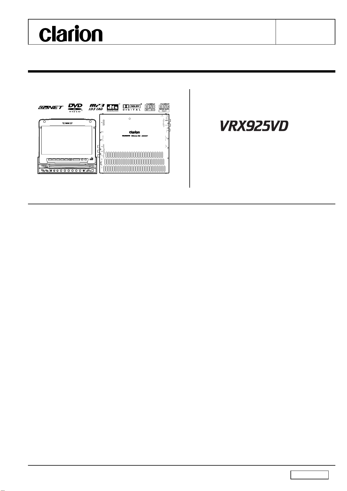
Service Manual
AM/FM DVD Video/Video CD/CD/
R
R
MP3 Player/CD Changer Controller
with 7" LC Display
Model
(QC-6810B-B)
(for U.S.A./ Region No. "1")
TILTM.LADJ A-MLIST KEYPADMENU
D
P
T
I
O
O
S
P
C
W
STOP MUTE
E
U
P
R
123456
LOUDDVTIT LE MONISTOPDV SETUP
SPECIFICATIONS
FM tuner section
Frequency range: 87.9MHz to 107.9MHz(U.S.A.)
87.50MHz to 108.0MHz(ASIA/
OCEANIA)
Usable sensitivity: 9dBf
50dB quieting sensitivity:
15dBf
Alternate channel selectivity:
70dB
Stereo separation: 35dB(1kHz)
Frequency response: 30Hz to 15kHz(+3/-3dB)
AM tuner section
Frequency range: 530kHz to 1710kHz(U.S.A.)
531kHz to 1629kHz(ASIA/
OCEANIA)
Usable sensitivity: 25uV
DVD player section
System: Digital versatile disc system with
CDDA capable
Usable discs: DVD video disc,Compact disc
Frequency response: 20Hz to 22kHz(48kHz)(+1/-1dB)
Signal to noise ratio: 100dB(1kHz)IHF-A
Dynamic range: 100dB(1kHz)
Distortion: 0.01%
Audio amplifier section
Rated power output: 18W x 4(20Hz to 20kHz,1%,4 ohm)
Maximum power output:
200W(50W x 4 JEITA)
Speaker impedance: 4 ohm(4 to 8 ohm)
Input section
Video input: 1.0V+0.2/-0.2Vp-p
(input impedance 75 ohm)
(QC-6810K-B)
(for ASIA / Region No. "3")
(QC-6810K-C)
(for OCEANIA / Region No. "4")
Audio input: 130mV+60/-60mVrms(High)
600mV+80/-80mVrms(Mid)
840mV+100/-100mVrms(Low)
(input impedance 10k ohm or
greater)
Video output section
Video output: 1.0V+0.2/-0.2Vp-p(output imped-
ance 75 ohm)
LCD monitor section
Screen size: 7-inch wide type
(152mm Width x 85mm Height)
Display method: Transmission type TN Liquid
Crystal Display
Drive method: TFT(thin-film transistor) active
matrix driving
Pixels: 336,960(1440x234)
General
Power source voltage: 14.4V DC
(10.8 to 15.6V allowable)
Ground: Negative
Current consumption: 4.0A(1W)
Auto antenna rated current:
500mA less
Dimensions(mm): Main unit
178(W)x50(H)x165(D)
Tuner amp unit
178(W)x37.5(H)x209.5(D)
Remote control unit
54(W)x28.8(H)x155(D)
Weight: Main unit 2.3kg
Tuner amp unit 1.1kg
Remote control unit 70g
(including battery)
- 1 -
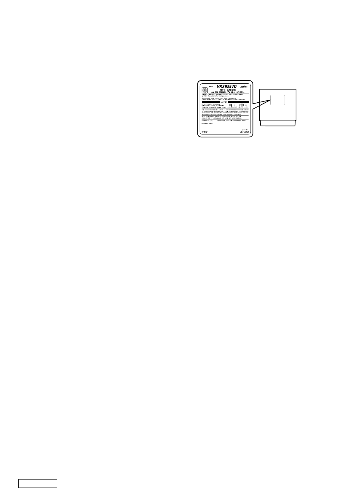
VRX925VD
Page 2
* Manufactured under license from Dolby Laboratories.
"Dolby" and the double-D symbol are trademarks of Dolby
Laboratories.Confidential Unpublished Works.c 19921997 Dolby Laboratories.All rights reserved.
* "DTS" are registered trademarks of Digital Theater
Systems,Inc.
* Specifications and design are subject to change without
notice for further improvement.
NOTES
* Use a CeNET extension cable that is less than 20m in
length.(including the Y-adapter CCA-519)
* We cannot supply PWB with component parts in prin-
ciple. When a circuit on PWB has failure , please repair
it by component parts base. Parts which are not mentioned in service manual are not supplied.
* This DVD player ca play the following discs.
DVD video discs,Video CDs,CD text,Audio CDs.
* This DVD video player cannot playback DVD-R,DVD-
RAM,DVD-ROM,CD-ROM,CD-RW,Photo CDs.
* This DVD player plays NTSC discs and PAL discs only
and cannot be used for playback of SECAM discs.
* Some CDs recorded in CD-R mode may not be usable.
* This slide mechanism is used the special adjustment jig
for repair.
COMPONENTS
QC-6810B-B/QC-6810K-B/K-C
Main unit ----------- 1
Remote control unit RCB-161-200 1
Battery(SUM-3) ----------- 2
Universal mounting bracket 300-9035-01 1
DCP case 335-6707-00 1
Antenna jumper 093-1465-03 1
Power supply lead(18P) 854-6392-50 1
Power supply lead(2P) 854-6393-51 1
Extension lead(20P to 20P) 855-0553-00 1
Outer escutcheon 940-7715-05 1
Parts bag -----------
Electro tap 060-0018-00 1
Machine screw(M4
Machine screw(M5
Sems hex. bolt(M5
Parts bag -----------
Hook plate 330-8216-01 2
Cord clamp 335-0833-01 1
Spacer 345-3653-01 1
Screw 716-0726-01 1
Parts bag -----------
Mounting bracket 300-7362-20 2
Canoe clip 335-2515-00 4
Machine screw(M4
Parts bag -----------
DCP lock spacer 345-5174-00 1
×3) 714-4003-87 4
×8) 714-5008-41 4
×8) 716-0496-01 5
×8) 714-4008-80 4
CAUTIONS
Use of controls,adjustment or performance of procedures
other than those specified herein,may result in hazardous
radiation exposure.
The COMPACT DISC player and MINI DISC player should
not be adjusted or repaired by anyone except properly qualified service personnel.
To engineers in charge of repair or
inspection of our products.
Before repair or inspection, make sure to follow
the instructions so that customers and Engineers
in charge of repair or inspection can avoid suffering any risk or injury.
1. Use specified parts.
The system uses parts with special safety features against
fire and voltage. Use only parts with equivalent characteristics when replacing them.
The use of unspecified parts shall be regarded as remodeling for which we shall not be liable. The onus of
product liability (PL) shall not be our responsibility in cases
where an accident or failure is as a result of unspecified
parts being used.
2. Place the parts and wiring back in their original positions
after replacement or re-wiring.
For proper circuit construction, use of insulation tubes,
bonding, gaps to PWB, etc, is involved. The wiring connection and routing to the PWB are specially planned
using clamps to keep away from heated and high voltage
parts. Ensure that they are placed back in their original
positions after repair or inspection.
If extended damage is caused due to negligence during
repair, the legal responsibility shall be with the repairing
company.
3. Check for safety after repair.
Check that the screws, parts and wires are put back securely in their original position after repair. Ensure for
safety reasons there is no possibility of secondary
ploblems around the repaired spots.
If extended damage is caused due to negligence of repair, the legal responsibility shall be with the repairing
company.
4. Caution in removal and making wiring connection to the
parts for the automobile.
Disconnect the battery terminal after turning the ignition
key off. If wrong wiring connections are made with the
battery connected, a short circuit and/or fire may occur.
If extensive damage is caused due to negligence of repair, the legal responsibility shall be with the repairing
company.
5. Cautions regarding chips.
- 2 -VRX925VD
Page 3
Do not reuse removed chips even when no abnormality
is observed in their appearance. Always replace them
with new ones. (The chip parts include resistors, capacitors, diodes, transistors, etc). The negative pole of tantalum capacitors is highly susceptible to heat, so use special care when replacing them and check the operation
afterwards.
6. Cautions in handling flexible PWB
Before working with a soldering iron, make sure that the
iron tip temperature is around 270
apply the iron tip repeatedly(more than three times)to the
same patterns. Also take care not to apply the tip with
force.
7. Turn the unit OFF during disassembly and parts replacement. Recheck all work before you apply power to the
unit.
8. Cautions in checking that the optical pickup lights up.
The laser is focused on the disc reflection surface through
the lens of the optical pickup. When checking that the
laser optical diode lights up, keep your eyes more than
30cms away from the lens. Prolonged viewing of the laser within 30cms may damage your eyesight.
. Take care not to
9. Cautions in handling the optical pickup
The laser diode of the optical pickup can be damaged by
electrostatic charge caused by your clothes and body.
Make sure to avoid electrostatic charges on your clothes
or body, or discharge static electricity before handling the
optical pickup.
9-1. Laser diode
The laser diode terminals are shorted for transportation in order to prevent electrostatic damage.
After replacement, open the shorted circuit. When
removing the pickup from the mechanism, short
the terminals by soldering them to prevent this
damage.
9-2. Actuator
The actuator has a powerful magnetic circuit. If a
magnetic material is put close to it. Its characteristics will change. Ensure that no foreign substances
enter through the ventilation slots in the cover.
9-3. Cleaning the lens
Dust on the optical lens affects performance. To
clean the lens, apply a small amount of isopropyl
alcohol to lens paper and wipe the lens gently.
SYSTEM CHECK
* The confirmation of connected equipment must be per-
formed for this unit only when the wiring connection is
complete and power is turned on to the unit first.When
the power is supplied,"PUSH PWR" appear in the
display.Press the FUNC button,the system check starts
inside the unit.When "COMPLETE" and "PUSH PWR"
appear alternately, press once again the FUNC button.
ERROR DISPLAYS
If an error occurs,one of the following displays is displayed.Take the measures described below to eliminate the problem.
Error display
DVD
player
CD
changer
MD
changer
ERROR 2
ERROR 3
ERROR 6
ERROR 2
ERROR 3
ERROR 6
ERROR H
EEROR 2
ERROR 3
ERROR 6
Note:If an error display other than the ones described above appears, press the reset button.
* When the reset button is pressed,frequencies of TV/radio stations,titles,etc. stored in memory are cleared.
Cause
A DVD is caught inside the DVD deck and is not ejected.
A DVD cannot be played due to scratches,etc.
A DVD is loaded upside-down inside the DVD deck and
does not play.
A CD inside the CD changer is not loaded.
A CD inside the CD changer cannot be played due to
scratches,etc.
A CD inside the CD changer cannot be played because
it is loaded upside-down.
Displayed when the temperature in the MD changer is
too high and playback has been stopped automatically.
An MD inside the MD changer is not loaded.
An MD inside the MD changer cannot be played due to
scratches,etc.
An MD inside the MD changer cannot be played because
it is loaded upside-down.
Displayed when a non-recorded MD is loaded in the MD
changer.
Measure
This is a failure of DVD deck's mechanism.
Replace with a non-scratched,non-warped disc.
Eject the disc then reload it properly.
This is a failure of CD changer's mechanism.
Replace with a non-scratched,non-warped disc.
Eject the disc then reload it properly.
Lower the surrounding temperature and wait for a
while to cool off MD changer.
This is a failure of MD changer's mechanism.
Replace with a non-scratched,non-warped disc.
Eject the disc then reload it properly.
Load a pre-recorded MD in the MD changer.
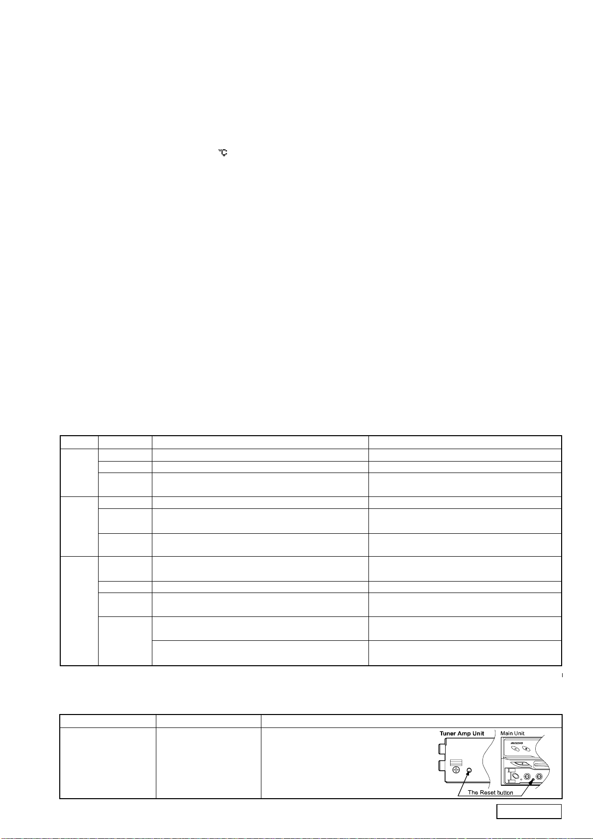
TROUBLESHOOTING
Problem
Nothing happens when
buttons are pressd.
Display is not accurate.
Cause
The microprocessor has
malfunction due to
noise,etc.
Measure
Turn off the power,then press the RELEASE lever and remove the DCP.Press
the Reset button both of tuner amp unit and
main unit for about 2 seconds with a thin
rod.When the reset button is pressed,turn
off the ACC power.
- 3 -
VRX925VD
Page 4
CLOCK ADJUSTMENT
1. When the panel is open,press the [ADJ] button to select
the ADJUST MOD menu.
2. Touch the [down] key to select "CLOCK".Touch the
[CLOCK] key to adjust the time.
3. Touch the [up],[down],[a.m] or [p.m] key to adjust the
time.
*The time is displayed in 12-hour format.
4. Press the [ADJ] button again or touch the [RTN] key two
times.The unit returns to the previous mode.
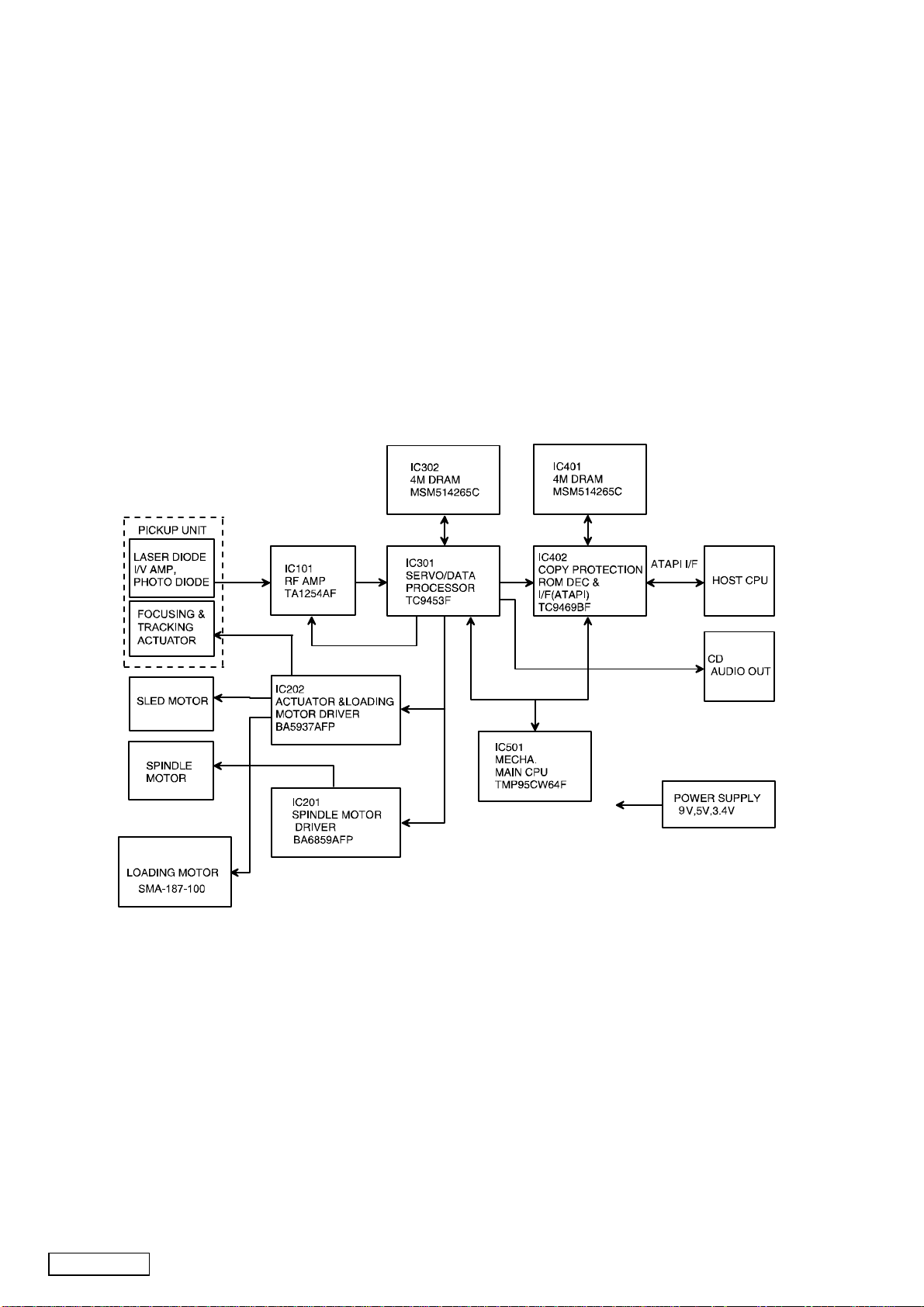
BLOCK DIAGRAM
DVD mechanism section
CHANGING THE RECEPTION AREA
This unit is initially set to USA(set to outside USA) frequency
intervals of 10kHz(9kHz) for AM and 200kHz(50kHz) for FM.
When using it outside the USA(in the USA),the frequency
reception range can be switched to the intervals below.
NOTE:( )ASIA/OCEANIA
SETTING THE RECEPTION AREA
While pressing [DISP] button, each time you press and hold
the number "6" of the [DIRECT] buttons for 2 seconds or
longer, the reception area switches from inside the USA to
outside the USA or from outside the USA to inside the USA.
* Any station preset memories are lost when the recep-
tion area is changed.
- 4 -VRX925VD
Page 5
Tuner amp unit section
- 5 -
VRX925VD
Page 6
Main unit section
SUB LCD PWB
SLIDE MECHANISM
PANEL SWITCH PWB
MAIN PWB-B
MAIN PWB-A
LCD PWB
H-DVD MECHANISM
MAIN PWB-C
- 6 -VRX925VD
INNER SWITCH PWB
Page 7

ADJUSTMENTS
Main unit section
DC-DC converter output voltage / PLL output voltage adjustment
Condition:
Function : VISUAL mode
Tuner amp unit : Input NTSC color bar video signal
1. Adjust VR150 so that the voltage of TP152 is
5.35V(+0.02V/-0.02V).
2. Adjust VR101 so that the voltage of TP105 is 1.6V(+0.1V/
-0.1V).
8. Burst cleaning adjustment
Input a color bar signal.(PAL)
Adjust L702 so that the wave form of TP711 is in focus.
VCOM DC bias adjustment
1. Adjust VR706(VCOM DC) to obtain the optimum
contrast(CINEMA MODE).
Voltage/frequency confirmation of inverter section
TP901 : 5.0V(+0.5V/-0.5V)
TP902 : 53kHz(+5kHz/-5kHz)
EXPLANATION OF IC
LCD PWB section
Power supply voltage confirmation
1. Make sure the voltage has become the following value
at each test point.
TP708 : 5.3V(+0.5V/-0.5V)
TP709 : 7.5V(+0.5V/-0.5V)
TP710 : 13.0V(+0.5V/-0.5V)
TP707 : -16.0V(+0.5V/-0.5V)
PLL adjustment
1. TP717 connect to GND. Confirm that the TP716 voltage
is 2.65V(+0.1V/-0.1V).
2. Adjust VR707 so that the frequency of TP718 is
15.734kHz(+50Hz/-50Hz).
Screen position adjustment
1. Adjust VR708 so that the pulse width of TP718 is 4.6u
sec(+0.1u sec./-0.1u sec.).
Voltage confirmation of J702 connector
VGH(pin32) : 13.0V(+0.5V/-0.5V)
VCC(pin24) : -11.0V(+0.5V/-0.5V)
VGL(pin18) : -8.4V(+0.5V/-0.5V)
VSH(pin1,pin3) : 5.3V(+0.5V/-0.5V)
VIDEO signal adjustment
(step 1 to 7 :NTSC, step 8 :PAL)
Input the visual signal(10step wave,monochrome,APL=50%,
1.0Vp-p)to the VIDEO input.
1. BRIGHT voltage confirmation
Make sure the voltage of TP701 is 2.00V(+0.1V/-0.1V).
2. GAMMA 0 voltage confirmation
Make sure the voltage of TP705 is 1.95V(+0.1V/-0.1V).
3. GAMMA 2 voltage confirmation
Make sure the voltage of TP706 is 2.15V(+0.1V/-0.1V).
4. RGB-AMP/CONT-G adjustment
Adjust VR705(RGB AMP) so that VBB voltage of TP712
is 4.0V(+0.05V/-0.05V).
Adjust VR701(CONT) so that VBW voltage of TP712 is
3.8V(+0.05V/-0.05V).
5. BRT-R Adjustment
Adjust VR703(BRT-R) so that VBB voltage of TP713 is
4.0V(+0.05V/-0.05V).
6. BRT-B Adjustment
Adjust VR704(BRT-B) so that VBB voltage of TP711 is
4.0V(+0.05V/-0.05V).
7. COM-AMP adjustment
Adjust VR702(COM-AMP) so that the amplitude of TP714
is 8.0V(+0.1V/-0.1V p-p).
051-6441-00 ES4408 DVD Processor
1.Terminal Description
pin 1: VCC : - : Positive supply voltage.
pin 2: LA 4 : O : Device address output.
pin 3: LA 5 : O : Device address output.
pin 4: LA 6 : O : Device address output.
pin 5: LA 7 : O : Device address output.
pin 6: LA 8 : O : Device address output.
pin 7: LA 9 : O : Device address output.
pin 8: VSS : - : Negative supply voltage.
pin 9: VCC : - : Positive supply voltage.
pin 10: LA 10 : O : Device address output.
pin 11: LA 11 : O : Device address output.
pin 12: LA 12 : O : Device address output.
pin 13: LA 13 : O : Device address output.
pin 14: LA 14 : O : Device address output.
pin 15: LA 15 : O : Device address output.
pin 16: LA 16 : O : Device address output.
pin 17: VSS : - : Negative supply voltage.
pin 18: VCC : - : Positive supply voltage.
pin 19: LA 17 : O : Device address output.
pin 20: LA 18 : O : Device address output.
pin 21: LA 19 : O : Device address output.
pin 22: LA 20 : O : Device address output.
pin 23: LA 21 : O : Device address output.
pin 24: RESET :IN : Reset signal input.
pin 25: TDM DX/RSEL :I/O: TDM transmit data output. ROM select
pin 26: VSS : - : Negative supply voltage.
pin 27: VCC : - : Positive supply voltage.
pin 28: TDM DR : IN : TDM receive data input.
pin 29: TDM CLK : IN : TDM clock pulse input.
pin 30: TDM FS : IN : TDM frame cynch.
pin 31: TDM TSC : O : TDM output enable.
pin 32: TWS/SEL PLL1 :I/O: Audio transmit frame synchronous pulse
pin 33: TSD0/SEL PLL0 :I/O: Audio transmit serial data output. Select
pin 34: VSS : - : Negative supply voltage.
pin 35: VCC : - : Positive supply voltage.
pin 36: TSD1/SEL PLL1 :I/O: Audio transmit serial data output. Select
pin 37: TSD 2 : O : Audio transmit serial data output.
pin 38: TSD 3 : O : Audio transmit serial data output.
pin 39: M CLK : O : The clock puse output to the CD IC.
pin 40: TB CK :I/O: Audio transmit bit clock.
pin 41: SPDIF DOBM : O : S/PDIF format output.
pin 42: NU : - : Not in use.
pin 43: VSS : - : Negative supply voltage.
pin 44: VCC : - : Positive supply voltage.
pin 45: RSD : IN: Audio receive serial data.
pin 46: RWS :IN : Audio receive frame synch.
pin 47: RBCK : IN : Audio receive bit clock.
pin 48: A PLL CAP : IN: Analog PLL capacitor.
pin 49: X IN : IN : Crystal connection.
pin 50: X OUT : O : Crystal connection.
pin 51: VCC : - : Positive supply voltage.
pin 52: VSS : - : Negative supply voltage.
pin 53: DMA 0 : O : DRAM address output.
pin 54: DMA 1 : O : DRAM address output.
input.
output. Select PLL input.
PLL input.
PLL input.
- 7 -
VRX925VD
Page 8

pin 55: DMA 2 : O : DRAM address output.
pin 56: DMA 3 : O : DRAM address output.
pin 57: DMA 4 : O : DRAM address output.
pin 58: DMA 5 : O : DRAM address output.
pin 59: VCC : - : Positive supply voltage.
pin 60: VSS : - : Negative supply voltage.
pin 61: DMA 6 : O : DRAM address output.
pin 62: DMA 7 : O : DRAM address output.
pin 63: DMA 8 : O : DRAM address output.
pin 64: DMA 9 : O : DRAM address output.
pin 65: DMA 10 : O : DRAM address output.
pin 66: DMA 11 : O : DRAM address output.
pin 67: VSS : - : Negative supply voltage.
pin 68: VCC : - : Positive supply voltage.
pin 69: DCAS : O : Column address strobe.
pin 70: DOE/DSCK EN :I/O: Output enable out. Clock enable in.
pin 71: DWE : O : DRAM write enable output.
pin 72: DRAS 0 : O : Raw address strobe output.
pin 73: DRAS 1 : O : Raw address strobe output.
pin 74: DRAS 2 : O : Raw address strobe output.
pin 75: VCC : - : Positive supply voltage.
pin 76: VSS : - : Negative supply voltage.
pin 77: D B 0 :I/O: DRAM data input/output.
pin 78: D B 1 :I/O: DRAM data input/output.
pin 79: D B 2 :I/O: DRAM data input/output.
pin 80: D B 3 :I/O: DRAM data input/output.
pin 81: DB 4 :I/O: Test mode LCD driver control DB.
pin 82: DB 5 :I/O: Test mode LCD driver control DB.
pin 83: VCC : - : Positive supply voltage.
pin 84: VSS : - : Negative supply voltage.
pin 85: DB 6 :I/O: Test mode LCD driver control DB.
pin 86: DB 7 :I/O: Test mode LCD driver control DB.
pin 87: D B 8 :I/O: DRAM data input/output.
pin 88: D B 9 :I/O: DRAM data input/output.
pin 89: DB 10 :I/O: DRAM data input/output.
pin 90: DB 11 :I/O: DRAM data input/output.
pin 91: VSS : - : Negative supply voltage.
pin 92: VCC : - : Positive supply voltage.
pin 93: DB 12 :I/O: DRAM data input/output.
pin 94: DB 13 :I/O: DRAM data input/output.
pin 95: DB 14 :I/O: DRAM data input/output.
pin 96: DB 15 :I/O: DRAM data input/output.
pin 97: DCS 1 : O : SDRAM chip select output.
pin 98: VSS : - : Negative supply voltage.
pin 99: VCC : - : Positive supply voltage.
pin100: DCS 0 : O : SDRAM chip select output.
pin101: DQM : O : Data input/output mask.
pin102: DSCK : O : Clock to SDRAM.
pin103: VSS : - : Negative supply voltage.
pin104: VCC : - : Positive supply voltage.
pin105: D Clock : O : BRI,COL,HUE setting signal output for the
pin106: YUV 0 : O : 8-bit YUV output.
pin107: YUV 1 : O : 8-bit YUV output.
pin108: YUV 2 : O : 8-bit YUV output.
pin109: YUV 3 : O : 8-bit YUV output.
pin110: YUV 4 : O : 8-bit YUV output.
pin111: VCC : - : Positive supply voltage.
pin112: VSS : - : Negative supply voltage.
pin113: YUV 5 : O : 8-bit YUV output.
pin114: YUV 6 : O : 8-bit YUV output.
pin115: YUV 7 : O : 8-bit YUV output.
pin116: P CLK 2X SCN :I/O:2x pixel clock.
pin117: P CLK Q SCN :I/O:Pixel clock.
pin118: VSYNCH :I/O: Vertical synch for screen video interface,
pin119: HSYNCH :I/O: Horizontal synch for screen video inter-
pin120: VSS : - : Negative supply voltage.
pin121: VCC : - : Positive supply voltage.
pin122: HD 0/DCI 0 :I/O:Host data & DCI data input/output.
pin123: HD 1/DCI 1 :I/O:Host data & DCI data input/output.
pin124: HD 2/DCI 2 :I/O:Host data & DCI data input/output.
pin125: HD 3/DCI 3 :I/O:Host data & DCI data input/output.
pin126: HD 4/DCI 4 :I/O:Host data & DCI data input/output.
pin127: HD 5/DCI 5 :I/O:Host data & DCI data input/output.
LCD.
programmable for rising or falling edge.
face, programmable for rising or falling
edge.
pin128: HD 6/DCI 6 :I/O:Host data & DCI data input/output.
pin129: VSS : - : Negative supply voltage.
pin130: VCC : - : Positive supply voltage.
pin131: HD 7/DCI 7 :I/O:Host data & DCI data input/output.
pin132: HD 8/DCI FDS :I/O: Host data input/output & DCI FDS.
pin133: HD 9 :I/O: Host data input/output.
pin134: HD 10 :I/O: Host data input/output.
pin135: HD 11 :I/O: Host data input/output.
pin136: HD 12 :I/O: Host data input/output.
pin137: HD 13 :I/O: Host data input/output.
pin138: VSS : - : Negative supply voltage.
pin139: VCC : - : Positive supply voltage.
pin140: HD 14 :I/O: Host data input/output.
pin141: HD 15 :I/O: Host data input/output.
pin142: HWRQ : O : Host write request.
pin143: HRDQ : O : Host read request.
pin144: HIRQ/DCI ERR :I/O: Host interrupt.
pin145: HRST : O : Host reset.
pin146: HIORDI : I : Host I/O ready.
pin147: VSS : - : Negative supply voltage.
pin148: VCC : - : Positive supply voltage.
pin149: HWR :I/O: Host write signal input / DCI interface
pin150: HRD : O : Host read signal output / DCI interface
pin151: HIOCS16 :IN : Device 16-bit data transfer.
pin152: HCS1FX : O : Host select 1.
pin153: HCS3FX : O : Host select 3.
pin154: HA 0 :I/O: Host address bus.
pin155: HA 1 :I/O: Host address bus.
pin156: VSS : - : Negative supply voltage.
pin157: VCC : - : Positive supply voltage.
pin158: HA 2 :I/O: Host address bus.
pin159: VPP : - : Connect to ground.
pin160: AUX 0 :I/O: Auxiliary input/output.
pin161: AUX 1 :I/O: Auxiliary input/output.
pin162: AUX 2 :I/O: Auxiliary input/output.
pin163: VSS : - : Negative supply voltage.
pin164: VCC : - : Positive supply voltage.
pin165: AUX 3 :I/O: Auxiliary input/output.
pin166: AUX 4 :I/O: Auxiliary input/output.
pin167: AUX 5 :I/O: Auxiliary input/output.
pin168: AUX 6 :I/O: Auxiliary input/output.
pin169: AUX 7 :I/O: Auxiliary input/output.
pin170: LOE : O : Device output enable.
pin171: VSS : - : Negative supply voltage.
pin172: VCC : - : Positive supply voltage.
pin173: LCS 0 : O : Chip select output.
pin174: LCS 1 : O : Chip select output.
pin175: LCS 2 : O : Chip select output.
pin176: LCS 3 : O : Chip select output.
pin177: VSS : - : Negative supply voltage.
pin178: L D 0 :I/O: Device data input/output.
pin179: L D 1 :I/O: Device data input/output.
pin180: L D 2 :I/O: Device data input/output.
pin181: L D 3 :I/O: Device data input/output.
pin182: L D 4 :I/O: Device data input/output.
pin183: VCC : - : Positive supply voltage.
pin184: VSS : - : Negative supply voltage.
pin185: L D 5 :I/O: Device data input/output.
pin186: L D 6 :I/O: Device data input/output.
pin187: L D 7 :I/O: Device data input/output.
pin188: L D 8 :I/O: Device data input/output.
pin189: L D 9 :I/O: Device data input/output.
pin190: LD 10 :I/O: Device data input/output.
pin191: LD 11 :I/O: Device data input/output.
pin192: VSS : - : Negative supply voltage.
pin193: VCC : - : Positive supply voltage.
pin194: LD 12 :I/O: Device data input/output.
pin195: LD 13 :I/O: Device data input/output.
pin196: LD 14 :I/O: Device data input/output.
pin197: LD 15 :I/O: Device data input/output.
pin198: LWRLL : O : Device write enable.
pin199: LWRHL : O : Device write enable.
pin200: VSS : - : Negative supply voltage.
pin201: VCC : - : Positive supply voltage.
acknowledge signal output.
clock output.
- 8 -VRX925VD
Page 9

pin202: NU : - : Not in use.
pin203: NU : - : Not in use.
pin204: LA 0 : O : Device address output.
pin205: LA 1 : O : Device address output.
pin206: LA 2 : O : Device address output.
pin207: LA 3 : O : Device address output.
pin208: VSS : - : Negative supply voltage.
052-5041-51 TMP95CW64F-3UR6(Z) DVD Mechanism Controller
1.Terminal Description
pin 1: A Vref :IN : Reference voltage for the internal ADC.
pin 2: A VSS : - : Analog ground.
pin 3: A VCC : - : Positive supply voltage for the internal
pin 4: NU : - : Not in use.
pin 5: NU : - : Not in use.
pin 6: Connect 7 :IN : Connect to pin7.
pin 7: EJECT SW :IN : Eject switch signal input.
pin 8: A MUTE : O : The audio mute signal output.
pin 9: SYS P 1 : O : System power 1 control signal output.
pin 10: NU : - : Not in use.
pin 11: RESET : O : Reset signal output.
pin 12: TEST 0 : O : For the test.
pin 13: TEST 1 : O : For the test.
pin 14: TEST 2 : O : For the test.
pin 15: TEST 3 : O : For the test.
pin 16: MCW : O : Loading motor control output.
pin 17: MCCW : O : Loading motor control output.
pin 18: TX D2 : O : The serial data output.
pin 19: RX D2 : IN : The serial data input.
pin 20: DVD R DE CS : O : The chip select signal output to the DVD
pin 21: DVD PRO CS : O : The chip enable signal output to DVD
pin 22: NU : - : Not in use.
pin 23: SPNDL CNT : O : Spindle control output.
pin 24: NU : - : Not in use.
pin 25: VCC : - : Positive supply voltage.
pin 26: GND : - : Ground.
pin 27: X 1 : - : Crystal connection.
pin 28: X 2 : - : Crystal connection.
pin 29: CNNCT VCC : IN : Connect to VCC.
pin 30: RESET :IN : Reset signal input.
pin 31: ACC CNT :IN : ACC ON signal input.
pin 32: NU : - : Not in use.
pin 33: LE TIME : O : For loading/eject time.
pin 34: FG PULSE :IN : FG pulse input.
pin 35: DISC MT SHRT :IN : Disc motor short brake.
pin 36: DATA REQ : O : The data request.
pin 37: D PRO INT :IN : The interrupt signal input from DVD pro-
pin 38: CMMD DT REQ : O : The command data request output.
pin 39: REM 5V : O : Power ON signal output to the 5V supply
pin 40: ID CONTINUE : O : ID check.
pin 41: DVD R DE INT :IN : The interrupt signal input from the DVD
pin 42: NU : - : Not in use.
pin 43: DVD R DE RST: O : The reset signal output to the DVD ROM
pin 44: VCC : - : Positive supply voltage.
pin 45: D 0 :I/O: Data input/output.
pin 46: D 1 :I/O: Data input/output.
pin 47: D 2 :I/O: Data input/output.
pin 48: D 3 :I/O: Data input/output.
pin 49: D 4 :I/O: Data input/output.
pin 50: D 5 :I/O: Data input/output.
pin 51: D 6 :I/O: Data input/output.
pin 52: D 7 :I/O: Data input/output.
pin 53: TEST 4 : O : For the test.
pin 54: TEST 5 : O : For the test.
pin 55: TEST 6 : O : For the test.
pin 56: TEST 7 : O : For the test.
pin 57: TEST 8 :I/O: For the test.
pin 58: TEST 9 :I/O: For the test.
pin 59: TEST 10 :I/O: For the test.
analog section.
ROM decoder.
processor.
cessor.
circuit.
ROM decoder.
decoder.
pin 60: TEST 11 :I/O: For the test.
pin 61: CNNCT VCC : IN : Connect to VCC.
pin 62: GND : - : Ground.
pin 63: VCC : - : Positive supply voltage.
pin 64: BUSY OUT : O : Busy flag output.
pin 65: DISC : O : Disc distinction signal output.
pin 66: LAYER : O : Layer distinction signal output.
pin 67: NU : - : Not in use.
pin 68: CHUKING :IN : The chucking switch signal input.
pin 69: DVD MCH S 1 : IN : The sensor signal input from DVD mech-
pin 70: DVD MCH S 2 : IN : The sensor signal input from DVD mech-
pin 71: DVD MCH S 3 : IN : The sensor signal input from DVD mech-
pin 72: NU : - : Not in use.
pin 73: NU : - : Not in use.
pin 74: NU : - : Not in use.
pin 75: NU : - : Not in use.
pin 76: MA : O : MA.
pin 77: NU : - : Not in use.
pin 78: NU : - : Not in use.
pin 79: NU : - : Not in use.
pin 80: A D 7 : O : Address output.
pin 81: A D 6 : O : Address output.
pin 82: A D 5 : O : Address output.
pin 83: A D 4 : O : Address output.
pin 84: A D 3 : O : Address output.
pin 85: A D 2 : O : Address output.
pin 86: A D 1 : O : Address output.
pin 87: A D 0 : O : Address output.
pin 88: RD STRB : O : The read strobe output.
pin 89: WR STRB : O : The write strobe output.
pin 90: NU : - : Not in use.
pin 91: GND : - : Ground.
pin 92: TEST 12 : IN : For the test.
pin 93: TEST 13 : IN : For the test.
pin 94: TEST 14 : IN : For the test.
pin 95: TEST 15 : IN : For the test.
pin 96: TEST 16 : IN : For the test.
pin 97: TEST 17 : IN : For the test.
pin 98: LIMIT SNC :IN : The inside limit signal input from the
pin 99: NU : - : Not in use.
pin100: Vref H : - : Reference voltage.
anism.
anism.
anism.
mechanism.
052-6056-00 M30622MAA-F43GP Master System controller
1.Terminal Description
pin 1: SPEED PULSE : IN: The speed pulse input.
pin 2: TIME BASE : IN : Time base pulse input.
pin 3: SPEED SEL 1 : O : The time constant select signal output for
pin 4: SPEED SEL 2 : O : The time constant select signal output for
pin 5: RDS CLK : IN: RDS clock pulse input.
pin 6: BYTE : IN : Input "L" at single mode operation.
pin 7: CN VSS : IN: Input "L" at single mode operation.
pin 8: SYS ACC : O : ACC detect signal output.
pin 9: NU : - : Not in use.
pin 10: RESET : IN : Reset signal input.
pin 11: X OUT : O : Crystal connection.
pin 12: VSS : - : Negative supply voltage.
pin 13: X IN : IN : Crystal connection.
pin 14: VCC : - : Positive supply voltage.
pin 15: NMI :IN : Connect to VCC.
pin 16: ACC DET :IN : ACC detection signal input.
pin 17: BU DET : IN : Backup detection signal input.
pin 18: MST REQ : IN: The master request signal input.
pin 19: 27pinConnect : IN : Connect to pin 27.
pin 20: AMP REM DT : IN: Remote controller wire short detection.
pin 21: EX AMP REM : O : The external amplifier control signal out-
pin 22: NU : - : Not in use.
pin 23: SLAVE ON : O : Slave ON signal output.
pin 24: BUS IN OUT : O : The audio selection signal output for Ce-
pin 25: NU : - : Not in use.
the speed pulse counter.
the speed pulse counter.
put.
NET.
- 9 -
VRX925VD
Page 10

pin 26: NU : - : Not in use.
pin 27: S D IN : IN: The serial data input.
pin 28: S D OUT : O : The serial data output.
pin 29: NU : - : Not in use.
pin 30: NU : - : Not in use.
pin 31: NU : - : Not in use.
pin 32: PLL CE : O : The chip enable signal output to the PLL
pin 33: PLL DO : O : Serial data output to the PLL IC.
pin 34: PLL DI : IN : Serial data input from the PLL IC.
pin 35: PLL SCLK : O : The clock pulse output for PLL.
pin 36: NU : - : Not in use.
pin 37: NU : - : Not in use.
pin 38: NU : - : Not in use.
pin 39: NU : - : Not in use.
pin 40: NU : - : Not in use.
pin 41: FLASH WR : IN : The write flag input from the flash mem-
pin 42: VOL CLK : O : The clock pulse output to the volume IC.
pin 43: VOL DO : O : Serial data output to the volume IC.
pin 44: AREA 1 : IN : The destination setting input.
pin 45: AREA 2 : IN : The destination setting input.
pin 46: 8p Navi Mute : O : 8pin navigation audio mute signal output.
pin 47: CeN Navi Mute : O : Ce-NET navigation audio mute signal out-
pin 48: AUDIO SEL : O : The audio source select signal output.
pin 49: SEL 2 : IN: The selection signal input.
pin 50: SEL 3 : IN: The selection signal input.
pin 51: V2 SEL 2 :IN : The selection signal input.
pin 52: V3 SEL 3 :IN : The selection signal input.
pin 53: F Image Sel 1 : O : The front image source selection signal
pin 54: F Image Sel 2 : O : The front image source selection signal
pin 55: F Image Sel 3 : O : The front image source selection signal
pin 56: R Image Sel 1 : O : The rear image source selection signal
pin 57: R Image Sel 2 : O : The rear image source selection signal
pin 58: R Image Sel 3 : O : The rear image source selection signal
pin 59: R Image Sel 4 : O : The rear image source selection signal
pin 60: VCC : - : Positive supply voltage.
pin 61: NU : - : Not in use.
pin 62: VSS : - : Negative supply voltage.
pin 63: NU : - : Not in use.
pin 64: R Image Sel 5 : O : The rear image source selection signal
pin 65: FM ST/SD :IN: At receiving the FM station, this port de-
pin 66: NOISE DISCH : O : The noise discharge command output for
pin 67: MUTE SPD UP : O : Station detection speed up command out-
pin 68: Diagnosis : O : For the diagnosis.
pin 69: RDS MUTE : O : RDS mute signal output.
pin 70: RDS DATA : IN: RDS serial data input.
pin 71: NU : - : Not in use.
pin 72: SYS MUTE : O : System muting signal output.
pin 73: 5V ON : O : The ON command output to the power
pin 74: AV ON : O : The ON command output to the power
pin 75: DVD 8V ON : O : The ON command output to the power
pin 76: A ANT REM : O : The automatic antenna control signal out-
pin 77: LINE MUTE : O : The line mute signal output.
pin 78: NU : - : Not in use.
pin 79: AMP MUTE : O : Muting signal output to the Audio Power
pin 80: AMP REM OUT : O : Amplifier ON signal output terminal.
pin 81: PHONE INT : IN : The telephone interrupt signal input.
pin 82: ILL DET : IN : Illumination ON signal input.
pin 83: PKB : IN : The parking brake signal input.
pin 84: NU : - : Not in use.
pin 85: NU : - : Not in use.
IC.
ory.
put.
output.
output.
output.
output.
output.
output.
output.
output.
tects the stereo signal. And at seeking or
scanning, this port detects the station
detection signal.
RDS.
put for RDS.
supply section.
supply section.
supply section.
put.
Amplifier.
pin 86: NU : - : Not in use.
pin 87: NU : - : Not in use.
pin 88: NU : - : Not in use.
pin 89: S METER :IN : The input terminal of internal A/D convert-
pin 90: NOISE : IN : The noise level for RDS.
pin 91: SPAN DATA : IN : The serial data input from the spectrum
pin 92: NU : - : Not in use.
pin 93: NU : - : Not in use.
pin 94: A VSS : - : Analog ground.
pin 95: NU : - : Not in use.
pin 96: A Vref : IN : Reference voltage for the internal ADC.
pin 97: A VCC : - : Positive supply voltage for the internal
pin 98: SPAN A : O : Spectrum analyzer band selection.
pin 99: SPAN B : O : Spectrum analyzer band selection.
pin100: SPAN C : O : Spectrum analyzer band selection.
er to monitor the radio field strength.
analyzer.
analog section.
052-6058-00 MR27V802D-37TPZA00 8M bit One Time PROM
1.Terminal Description
pin 1: NU : - : Not in use.
pin 2: A 18 :IN : The address input.
pin 3: A 17 :IN : The address input.
pin 4: A 7 : IN : The address input.
pin 5: A 6 : IN : The address input.
pin 6: A 5 : IN : The address input.
pin 7: A 4 : IN : The address input.
pin 8: A 3 : IN : The address input.
pin 9: A 2 : IN : The address input.
pin 10: A 1 :IN : The address input.
pin 11: A 0 :IN : The address input.
pin 12: Chip enable : IN: Chip enable signal input.
pin 13: VSS : - : Ground.
pin 14: Output enable : IN : Output enable signal input.
pin 15: D 0 : O : The data output.
pin 16: D 8 : O : The data output.
pin 17: D 1 : O : The data output.
pin 18: D 9 : O : The data output.
pin 19: D 2 : O : The data output.
pin 20: D 10 : O : The data output.
pin 21: D 3 : O : The data output.
pin 22: D 11 : O : The data output.
pin 23: VCC : - : Positive supply voltage.
pin 24: D 4 : O : The data output.
pin 25: D 12 : O : The data output.
pin 26: D 5 : O : The data output.
pin 27: D 13 : O : The data output.
pin 28: D 6 : O : The data output.
pin 29: D 14 : O : The data output.
pin 30: D 7 : O : The data output.
pin 31: D 15 / A -1 :I/O: The data output. / The address input.
pin 32: VSS : - : Ground.
pin 33: BYTE : IN : 8bit/16bit selection.
pin 34: A 16 : IN : The address input.
pin 35: A 15 : IN : The address input.
pin 36: A 14 : IN : The address input.
pin 37: A 13 : IN : The address input.
pin 38: A 12 : IN : The address input.
pin 39: A 11 : IN : The address input.
pin 40: A 10 : IN : The address input.
pin 41: A 9 :IN : The address input.
pin 42: A 8 :IN : The address input.
pin 43: NU : - : Not in use.
pin 44: NU : - : Not in use.
052-7055-20 NZX0100-1801L Touch-panel & Sub-LCD Controller
1.Terminal Description
pin 1: C 1 : - : Not in use.
pin 2: VL 1 : IN : Positive voltage input for the LCD.
pin 3: LCD ON : O : LCD back light ON signal output.
pin 4: GREEN 1 : O : The LED drive output.
pin 5: AMBER 1 : O : The LED drive output.
pin 6: AUT DIMM :IN: The automatic dimmer signal input.
- 10 -VRX925VD
Page 11

pin 7: Y R IN : IN: The input terminal of the internal ADC.
pin 8: X R IN : IN: The input terminal of the internal ADC.
pin 9: Y G IN : IN : The input terminal of the internal ADC.
pin 10: X G IN :IN : The input terminal of the internal ADC.
pin 11: KS OUT 2 : O : Key scan output.
pin 12: KS OUT 1 : O : Key scan output.
pin 13: KS OUT 0 : O : Key scan output.
pin 14: DIMMER : O : PWM output.
pin 15: KS IN 3 : IN : Key scan input.
pin 16: KS IN 2 : IN : Key scan input.
pin 17: KS IN 1 : IN : Key scan input.
pin 18: KS IN 0 : IN : Key scan input.
pin 19: GREEN 2 : O : The LED drive output.
pin 20: AMBER 2 : O : The LED drive output.
pin 21: TXD : O : The serial data output.
pin 22: RXD : IN : The serial data input.
pin 23: ST0 :IN : Connect to the ground.
pin 24: TPW : IN : The touch panel control input.
pin 25: PA :I/O: The touch panel control input/output.
pin 26: CHK : O : The touch panel control output.
pin 27: Y- : O : The touch panel control output.
pin 28: X- : O : The touch panel control output.
pin 29: Y+ : O : The touch panel control output.
pin 30: X+ : O : The touch panel control output.
pin 31: REQ O : O : Transmit request signal output.
pin 32: BUSY :IN : The busy flag input.
pin 33: KS OUT 3 : O : Key scan output.
pin 34: NU : - : Not in use.
pin 35: RESET : IN : Reset signal input.
pin 36: BLUE OUT : O : The LED drive output.
pin 37: P 7 : O : FL ON
pin 38 : X IN :IN : Crystal connection.
pin 39: X OUT : O : Crystal connection.
pin 40: VSS : - : Negative supply voltage.
pin 41: P 5 : O : VIDEO / RGB
pin 42: P 1 : O : MODE S
pin 43: DATA : O : DATA
pin 44: LOAD : O : LOAD
pin 45: CLOCK : O : The clock pulse output.
pin 46: P 4 : O : CLAMP
pin 47: P 6 : O : VIDEO / MUTE
pin 48: P 0 : O : NTSC / PAL
pin 49: P 3 : O : MODE N
pin 50: P 2 : O : MODE W
pin 51: SEG 39 : O : The segment output.
pin 52: SEG 38 : O : The segment output.
pin 53: SEG 37 : O : The segment output.
pin 54: SEG 36 : O : The segment output.
pin 55: SEG 35 : O : The segment output.
pin 56: SEG 34 : O : The segment output.
pin 57: SEG 33 : O : The segment output.
pin 58: SEG 32 : O : The segment output.
pin 59: SEG 31 : O : The segment output.
pin 60: SEG 30 : O : The segment output.
pin 61: SEG 29 : O : The segment output.
pin 62: SEG 28 : O : The segment output.
pin 63: SEG 27 : O : The segment output.
pin 64: SEG 26 : O : The segment output.
pin 65: SEG 25 : O : The segment output.
pin 66: SEG 24 : O : The segment output.
pin 67: SEG 23 : O : The segment output.
pin 68: SEG 22 : O : The segment output.
pin 69: SEG 21 : O : The segment output.
pin 70: SEG 20 : O : The segment output.
pin 71: SEG 19 : O : The segment output.
pin 72: SEG 18 : O : The segment output.
pin 73: SEG 17 : O : The segment output.
pin 74: SEG 16 : O : The segment output.
pin 75: SEG 15 : O : The segment output.
pin 76: SEG 14 : O : The segment output.
pin 77: SEG 13 : O : The segment output.
pin 78: SEG 12 : O : The segment output.
pin 79: SEG 11 : O : The segment output.
pin 80: SEG 10 : O : The segment output.
pin 81:SEG 9 : O : The segment output.
pin 82:SEG 8 : O : The segment output.
pin 83: SEG 7 : O : The segment output.
pin 84: SEG 6 : O : The segment output.
pin 85: SEG 5 : O : The segment output.
pin 86: SEG 4 : O : The segment output.
pin 87: SEG 3 : O : The segment output.
pin 88: SEG 2 : O : The segment output.
pin 89: SEG 1 : O : The segment output.
pin 90: SEG 0 : O : The segment output.
pin 91: VCC : - : Positive supply voltage.
pin 92: Vref : - : Reference voltage.
pin 93: A Vss : - : Analog ground.
pin 94: COMMON 3 : O : The common signal output.
pin 95: COMMON 2 : O : The common signal output.
pin 96: COMMON 1 : O : The common signal output.
pin 97: COMMON 0 : O : The common signal output.
pin 98: VL 3 : IN : Positive supply voltage for LCD.
pin 99: VL 2 : IN : Positive supply voltage for LCD.
pin100: C 2 : - : Not in use.
052-7062-01 uPD703037AGF-A14-3BA Main Display Controller
1.Terminal Description
pin 1: NU : - : Not in use.
pin 2: ESS CK : IN : The clock pulse input from DVD Signal
pin 3: ESS RST : O : The reset pulse output to DVD Signal
pin 4: DVD ACC ON : O : DVD ACC ON.
pin 5: DVD EJECT : O : DVD EJECT.
pin 6: TP RX : IN : The serial data input from the touch pan-
pin 7: TP TX : O : The serial data output to the touch pan-
pin 8: TP REQ : IN : The request signal from the touch panel.
pin 9: VDD : - : Positive supply voltage.
pin 10: VSS : - : Negative supply voltage.
pin 11: TP RST : O : The reset pulse output to the touch pan-
pin 12: BEEP : O : Beep out.
pin 13: DVD 8V DET :IN : DVD 8V detection.
pin 14: KS IN 0 : IN : Key scan input.
pin 15: KS IN 1 : IN : Key scan input.
pin 16: IRI : IN : The remote control signal input.
pin 17: KS IN 2 : IN : Key scan input.
pin 18: KS IN 3 : IN : Key scan input.
pin 19: KS OUT 0 : O : Key scan output.
pin 20: KS OUT 1 : O : Key scan output.
pin 21: FLASH PRG : IN: The flash memory program command in-
pin 22: KS OUT 2 : O : Key scan output.
pin 23: GREEN : O : Signal output for the LED.
pin 24: AMBER : O : Signal output for the LED.
pin 25: BLINK LED : O : Signal output for the LED.
pin 26: IE RX : IN: IE-Bus serial data intput.
pin 27: IE TX : O : IE-Bus serial data output.
pin 28: EEP DI : IN : The serial data input from EEP-ROM.
pin 29: EEP DO : O : The serial data output to EEP-ROM.
pin 30: EEP CLK : O : The clock pulse output to EEP-ROM.
pin 31: EEP CEO : O : The chip enable signal output to EEP-
pin 32: V SEL : O : The video select output.
pin 33: FLASH WR : IN: The write flag input from the flash ROM.
pin 34: RESET : IN : Reset signal input.
pin 35: PLL DOWN : IN : Not in use.
pin 36: NU : - : Not in use.
pin 37: REG CAPA : - : The capacitor connection.
pin 38: X OUT : O : Crystal connection.
pin 39: X IN : IN : Crystal connection.
pin 40: GND : - : Ground.
pin 41: VDD : - : Positive supply voltage.
pin 42: NU : - : Not in use.
pin 43: NAVI ON : O : NAVI ON signal output.
pin 44: BLKO : O : The blanking signal output.
pin 45: RGB ON : O : RGB ON signal output.
pin 46: UP/DWN MF : O : Up/Down motor control.
pin 47: UP/DWN MR : O : Up/Down motor control.
pin 48: OPN CLS MF : O : Open/Close motor control.
Processor.
Processor.
el.
el.
el.
put.
ROM.
- 11 -
VRX925VD
Page 12

pin 49: OPN CLS MR : O : Open/Close motor control.
pin 50: OSD CD 7 :I/O: The parallel data input/output for the on
pin 51: OSD CD 6 :I/O: The parallel data input/output for the on
pin 52: OSD CD 5 :I/O: The parallel data input/output for the on
pin 53: OSD CD 4 :I/O: The parallel data input/output for the on
pin 54: OSD CD 3 :I/O: The parallel data input/output for the on
pin 55: OSD CD 2 :I/O: The parallel data input/output for the on
pin 56: OSD CD 1 :I/O: The parallel data input/output for the on
pin 57: OSD CD 0 :I/O: The parallel data input/output for the on
pin 58: VDD : - : Positive supply voltage.
pin 59: GND : - : Ground.
pin 60: OSD RD : O : The read command output for the on
pin 61: OSD WR : O : The write command output for the on
pin 62: OSD CS : O : The chip select signal output to on screen
pin 63: OSD PS2 : O : On screen display port select.
pin 64: OSD PS1 : O : On screen display port select.
pin 65: OSD PS0 : O : On screen display port select.
pin 66: OSD RST : O : The reset pulse output for the on screen
pin 67: ROM EN : O : ROM enable signal output.
pin 68: PNL ON : O : The panel ON signal output.
pin 69: MTR PWR SEL : O : The voltage select signal output for the
pin 70: MTR ON : O : The motor ON signal output.
pin 71: DVD ON 2 : O : DVD ON signal output.
pin 72: DVD ON 1 : O : DVD ON signal output.
pin 73: AV ON : O : The ON command output to the power
pin 74: A VDD : - :Positive supply voltage for the Analog
pin 75: A VSS : - : Analog ground.
pin 76: A Vref : IN : Reference voltage for the internal ADC.
pin 77: OSD WAIT : IN : The wait signal input for the on screen
pin 78: INIT 1 : IN : The initial setting input.
pin 79: INIT 2 : IN : The initial setting input.
pin 80: INIT 3 : IN : The initial setting input.
pin 81: INIT 4 : IN : The initial setting input.
pin 82: INIT 5 : IN : The initial setting input.
pin 83: SYS PWR 1 : IN : System power ON signal input.
pin 84: PWR SW : IN: Power switch signal input.
pin 85: EJECT SW : IN : Eject switch signal input.
pin 86: OPEN SW : IN : Open switch signal input.
pin 87: TILT AD : IN: The input terminal of the internal ADC to
pin 88: OPEN AD : IN: The input terminal of the internal ADC to
pin 89: BU DET : IN : Backup detection signal input.
pin 90: SLAVE ON : IN : Slave ON signal input.
pin 91: DCP DET : IN : DCP detection siganl input.
pin 92: SW INT : IN : The switch signal input.
pin 93: ILL DET : IN : Illumination ON signal input.
pin 94: OSD INT : IN : The interrupt signal input for the on
pin 95: MST REQ : O : The master request signal output.
pin 96: ESS RESET : IN : The reset signal input from DVD Signal
pin 97: F END RST : O : The front end reset.
pin 98: ESS DO : O : The serial data output to DVD Signal Pro-
pin 99: ESS CK : O : The clock pulse output to DVD Signal
pin100: ESS DI :IN: The serial data input from DVD Signal
screen display.
screen display.
screen display.
screen display.
screen display.
screen display.
screen display.
screen display.
screen display.
screen display.
display.
display.
motors.
supply section.
section.
display.
sense the tilt.
detect the mechanism state.
screen display.
Processor.
cessor.
Processor.
Processor.
pin 3: A 17 :IN : The address input.
pin 4: A 7 : IN : The address input.
pin 5: A 6 : IN : The address input.
pin 6: A 5 : IN : The address input.
pin 7: A 4 : IN : The address input.
pin 8: A 3 : IN : The address input.
pin 9: A 2 : IN : The address input.
pin 10: A 1 :IN : The address input.
pin 11: A 0 :IN : The address input.
pin 12: Chip enable : IN: Chip enable signal input.
pin 13: VSS : - : Ground.
pin 14: Output enable : IN : Output enable signal input.
pin 15: D 0 : O : The data output.
pin 16: D 8 : O : The data output.
pin 17: D 1 : O : The data output.
pin 18: D 9 : O : The data output.
pin 19: D 2 : O : The data output.
pin 20: D 10 : O : The data output.
pin 21: D 3 : O : The data output.
pin 22: D 11 : O : The data output.
pin 23: VCC : - : Positive supply voltage.
pin 24: D 4 : O : The data output.
pin 25: D 12 : O : The data output.
pin 26: D 5 : O : The data output.
pin 27: D 13 : O : The data output.
pin 28: D 6 : O : The data output.
pin 29: D 14 : O : The data output.
pin 30: D 7 : O : The data output.
pin 31: D 15 / A -1 :I/O: The data output. / The address input.
pin 32: VSS : - : Ground.
pin 33: BYTE : IN : 8bit/16bit selection.
pin 34: A 16 : IN : The address input.
pin 35: A 15 : IN : The address input.
pin 36: A 14 : IN : The address input.
pin 37: A 13 : IN : The address input.
pin 38: A 12 : IN : The address input.
pin 39: A 11 : IN : The address input.
pin 40: A 10 : IN : The address input.
pin 41: A 9 :IN : The address input.
pin 42: A 8 :IN : The address input.
pin 43: A 19 : IN : The address input.
pin 44: NU : - : Not in use.
052-7063-01 MR27V1602F-OHCTP 16M bit One Time PROM
1.Terminal Description
pin 1: NU : - : Not in use.
pin 2: A 18 : IN : The address input.
- 12 -VRX925VD
Page 13
EXPLODED VIEW : PARTS LIST
Main unit 1/2 section
38
43
56
28
25
55
24
55
52
54
21
29
53
62
54
63
57
36
22
28
26
58
59
23
40
39
27
45
44
29
41
28
32
60
29
61
41
42
29
41
33
41
31
46
34
17
20
Note)Some parts depend on each model.The model name is specified in the description.
(B-B) : QC-6810B-B , (K-B) : QC-6810K-B , (K-C) : QC-6810K-C
1 370-9613-00 ESCUTCHEON 1
2 345-5186-00 SLIDER 2
3 382-6463-00 BUTTON EJECT 1
4 347-6795-00 SPACER 1
5 335-6729-00 BUTTON PLATE 1
6 039-2137-00 INNER SWITCH PWB 1
7 346-0151-00 LEATHER SHEET 1
8 335-6730-00 DICS GUIDE 1
9 335-6728-00 RELEASE LEVER 1
10 750-6729-00 SPRING 1
11 331-3391-00 DCP HOLDER 1
(WITHOUT COMPONENT)
30
37
35
15
51
4
2
56
3
8
7
15
49
50
10
2
49
48
12
47
19
18
13
14
15
9
16
1
NO. PART NO. DESCRIPTION Q'TYNO. PART NO. DESCRIPTION Q'TY
12 331-3392-00 DCP PLATE 1
13 750-6728-00 SPRING RELEASE 1
14 743-1500-20 E-RING 1
15 716-0872-02 PAD SCREW 10
16 335-6836-00 IR PLATE 1
17 DCP-396-601 DCP ASSY 1
18 746-0931-00 WASHER 1
19 746-0761-00 WASHER 2
20 781-2650-00 SCREW 2
21 331-3389-02 BRACKET A 1
22 331-3390-00 BRACKET B 1
20
19
11
- 13 -
VRX925VD
Page 14

23 313-1841-00 HEAT SINK 1
24 816-2584-00 FLAT WIRE(45P) 1
25 816-2585-00 FLAT WIRE(50P) 1
26 854-4547-50 EXTENSION LEAD 1
27 714-2610-81 MACHINE SCREW 2
28 039-2132-01 MAIN PWB 1
29 716-0878-00 IT-SCREW 5
30 929-2125-01 DVD MECHANISM MODULE 1
31 311-1853-00 LOWER CASE 1
32 331-3387-00 MECHANISM BRKT 1
33 331-3388-00 EARTH PLATE 1
34 286-9967-01 SETPLATE(B-B) 1
35 816-2582-00 FLAT WIRE(18P) 1
36 816-2583-00 FLAT WIRE(18P) 1
37 039-2147-00 FLEXIBLE PWB(DVD 50P) 1
38 855-0552-01 MULTI POLE CPRD 1
39 020-3045-00 FAN(DC-MOTOR) 1
40 780-2014-00 SCREW 2
41 714-2603-81 MACHINE SCREW 4
42 347-6794-00 SHIELD FILM 1
286-6120-00 SETPLATE(K-B)
286-6119-00 SETPLATE(K-C)
(WITHOUT COMPONENT)
NO. PART NO. DESCRIPTION Q'TYNO. PART NO. DESCRIPTION Q'TY
43 714-2604-81 MACHINE SCREW 2
44 345-5175-00 SPACER 1
45 345-5176-00 SPACER 1
46 290-8183-00 DTS LABEL 1
47 060-4008-00 IR-RECEIVER 1
48 013-7411-50 DETECTOR SWITCH 1
49 013-6507-50 LUMI SWITCH 3
50 013-6519-50 LUMI SWITCH 12
51 074-1287-70 OUTLET SOCKET(20P) 1
52 074-1125-02 OUTLET SOCKET(2P) 1
53 075-0385-00 JACK(OPTICAL) 1
54 074-1189-95 OUTLET SOCKET(45P) 2
55 074-1189-00 OUTLET SOCKET(50P) 2
56 074-1205-00 OUTLET SOCKET(50P) 2
57 074-1287-70 OUTLET SOCKET(20P) 1
58 076-0576-15 PLUG(15P) 1
59 076-0276-05 PLUG(5P) 1
60 060-0100-01 BUZZER 1
61 347-6796-00 PROTECT FILM 1
62 076-0488-02 PLUG(2P) 1
63 074-1100-68 OUTLET SOCKET(18P) 1
Main unit 2/2 section
1 039-2138-00 LCD PWB 1
2 039-2140-00 SUB LCD PWB 1
3 347-6783-00 REFLECTOR 1
4 335-6734-00 ILLUMI PLATE 1
5 347-6782-00 FILM 1
6 379-1237-41 INDICATOR(SUB LCD) 1
7 347-6805-00 SHADE 1
8 331-3408-00 S-LCD HOLDER 1
9 345-8739-01 SPACER 2
10 335-6731-00 S-LCD COVER 1
11 382-6465-00 BUTTON(DISP/OPN) 1
12 382-6464-00 BUTTON(+/-) 1
13 373-0983-00 DIAL COVER 1
14 378-0537-00 BADGE 1
15 716-3483-00 SCREW 2
16 716-1845-01 SCREW 2
17 781-2040-01 P-SCREW 4
18 370-9614-03 ESCUTCHEON(B-B) 1
19 371-5729-00 TRIM PLATE 1
20 335-6732-00 REFLECTOR 1
21 382-6466-00 BUTTON(A/N/TILT) 1
22 382-6467-00 BUTTON(6-PIECES) 1
23 382-6468-00 BUTTON(FF/REW) 1
24 039-2139-01 PANEL SWITCH PWB 1
25 716-0872-00 PAD SCREW 3
26 347-6834-00 SHADE 1
370-9614-06 ESCUTCHEON(K-B/K-C)
(WITHOUT COMPONENT)
(WITHOUT COMPONENT)
(WITHOUT COMPONENT)
NO. PART NO. DESCRIPTION Q'TYNO. PART NO. DESCRIPTION Q'TY
27 335-6491-01 ES-COVER(L) 1
28 335-6492-01 ES-COVER(R) 1
29 714-5008-41 MACHINE SCREW 2
30 750-3137-02 SPRING(L) 1
31 750-3137-03 SPRING(R) 1
32 714-2604-81 MACHINE SCREW 6
33 379-0458-10 INDICATOR(7INCH LCD) 1
34 013-9706-00 SWITCH ASSY 1
35 347-6450-00 DOUBLE FACE 1
36 347-6629-00 DOUBLE FACE 1
37 347-6085-00 DOUBLE FACE 4
38 345-8598-00 CUSHION 1
39 345-8618-01 CUSHION 2
40 347-6805-00 SHADE 1
41 383-0687-00 BADGE(CLARION) 1
42 345-8737-00 SHADE 2
43 716-1845-01 SCREW 3
44 347-6780-00 SHADE 1
45 948-0646-00 SLIDE MECHANISM ASSY 1
46 347-6586-00 MOTOR COVER 2
47 347-6451-00 DOUBLE FACE 4
48 347-6781-00 INSULATOR(LCD) 1
49 335-6733-00 UPPER TRIM 1
50 039-2144-00 FLEXIBLE PWB(50P) 1
51 781-2026-00 SCREW 5
52 781-1750-00 SCREW 4
53 738-2630-17 PRECISION SCREW 2
54 781-1722-00 SCREW 6
- 14 -VRX925VD
Page 15

25
24
67
25
14
11
10
13
22
26
54
54
59
18
424243
41
16
17
2
68
9
8
17
12
29
43
19
56
58
51
15
69
6
9
7
1
63
62
61
51
3
4
5
32
17
54
64
51
55
23
51
16
21
65
20
60
15
50
58
66
57
51
38
37
40
39
39
34
36
37
33
35
46
32
30
47
49
48
53
44
55 780-2003-00 SCREW 1
56 335-6776-00 SENSOR ILLUMI 1
57 345-5185-01 GASKET 1
58 345-8738-00 SPACER 2
59 347-6807-00 SPACER 2
60 347-5541-01 INSULATOR 1
61 076-0529-04 PLUG(4P) 1
62 074-1189-95 OUTLET SOCKET(45P) 1
28
53
52
45
32
27
31
47
NO. PART NO. DESCRIPTION Q'TYNO. PART NO. DESCRIPTION Q'TY
63 074-1189-85 OUTLET SOCKET(35P) 1
64 074-1205-82 OUTLET SOCKET(32P) 1
65 074-1275-58 OUTLET SOCKET(8P) 1
66 076-0645-80 PLUG(30P) 1
67 074-1276-80 OUTLET SOCKET(30P) 1
68 074-1296-64 OUTLET SOCKET(14P) 1
69 076-0663-64 PLUG(14P) 1
29
- 15 -
VRX925VD
Page 16

How to release the LCD module
T
50PIN SOCKE
C
I
M
L
L
50PIN FLEXIBLE PWB
A
B
H
I
D
F
F
1. Remove the screws(No.Ax2) and the springs(No.Bx2).
2. Remove the screws(No.Cx2,Dx4,Ex2) and release the flexible PWB(No.F).
3. Release the lower case with DVD
mechanism(No.G).Release the cover(No.Hx2).
4. Remove the screws(No.Ix6,Jx2,Kx4,Lx3) and release the
escutchen(No.M).
G
5. Pull out the LCD module(with switch ass'y) and release 32P/
8P/4P connectors.
C
E
D
H
J
Tuner amp unit section
12
8
23
5
4
2
11
17
1
22
6
18
21
K
19
11
20
10
13
12
B
3
7
24
14
16
11
A
NO. PART NO. DESCRIPTION Q'TY
1 039-2117-01 TUNER PWB 1
2 331-3407-00 FRONT PLATE 1
3 331-3405-00 OUTLET HOLDER 1
4 331-3406-00 IC HOLDER 1
5 313-1730-00 HEAT SINK 1
6 702-3008-81 TAP SCREW 3
7 714-3006-81 MACHINE SCREW 3
6
15
11
25
9
8 714-2612-81 MACHINE SCREW 3
9 311-1741-03 LOWER CASE 1
10 310-1649-03 UPPER CASE 1
11 716-0878-00 IT-SCREW 4
12 714-2605-81 MACHINE SCREW 4
13 013-5102-00 SLIDE SWITCH 1
14 074-1030-00 OUTLET SOCKET 2
15 092-0612-03 ANTENNA RECEPTACLE 1
16 880-2089K TUNER 1
17 074-1125-18 OUTLET SOCKET 1
18 074-1194-00 OUTLET SOCKET(13P) 1
19 074-1134-00 OUTLET SOCKET(20P) 1
20 075-0310-03 JACK 1
21 013-3949-00 SWITCH 1
22 075-9002-02 JACK(4P) 1
23 051-2038-10 IC(LA47501) 1
24 075-9001-00 JACK(6P) 1
25 073-0762-90 TERMINAL 1
(WITHOUT COMPONENT)
- 16 -VRX925VD
Page 17

DVD mechanism section
1
1-1
NO. PART NO. DESCRIPTION Q'TY
1 HBS-523-100 MECHANISM ASSY 1
1-1 SMA-187-100 LOADING MOTOR ASSY 1
2 039-1946-01 MAIN PWB 1
3 750-3450-01 DAMPER SPRING 4
4 620-0993-00 FRONT STOPPER 1
5 620-0994-01 CHASSIS 1
6 629-0078-02 DAMPER 4
7 716-1851-00 SCREW(M2×2) 4
8 716-1856-00 SCREW(M2×2) 1
9 716-1864-00 SCREW(M1.7×4.5) 3
10 074-1189-00 OUTLET SOCKET(50P) 1
11 074-1201-68 OUTLET SOCKET(18P) 2
12 074-1059-80 OUTLET SOCKET(30P) 1
13 013-7412-50 DETECTOR SWITCH 1
(WITHOUT COMPONENT)
HOW TO CHECK
When the mechanism assy HBS-523-100 is replaced,please
check the operation by the following procedure.
Preparation
1. Test disc
DVD : TDV-562(made by ALMEDIO)
CD : TCD-732RA(made by ALMEDIO)
Procedure
Operation check by test DVD(TDV-562)
10
11
2
8
3
7
3
7
6
4
6
9
3
7
6
12
13
3
5
7
6
9
1. Insert the test DVD and play chapter 16. Then,check the
access operation.
2. Play chapter 1. Then ,check the access operation.
3. If there is no problem,the operation must be OK.
Operation check by test CD(TCD-732RA)
1. Insert the test CD and play track 15. Then,check the jumping sound.
2. Play track 1. Then,check the jumping sound.
3. If there is no problem,the operation must be OK.
Checking standard
DVD play:Can be played without any stopping and
distortion.(more than 10 sec.)
CD play:Can be played correctly without jumping
9
sound.(more than 10 sec.)
Access operation:The access time from inner to outer and
outer to inner must be within 2.5 seconds.
ELECTRICAL PARTS LIST
Tuner PWB(B1) section
REF No. PART No. DESCRIPTION REF No. PART No. DESCRIPTION REF No. PART No. DESCRIPTION
BL501 880-2089K FM/AM TUNER
C502 166-2201-50 22pF CH
C503 166-1007-50 10pF CH
C506 042-0643-51 16V100uF
C507 168-1032-55 0.01uF
C508 168-2232-55 0.022uF
C509 043-0277-51 0.022uF
C510 166-1011-50 100pF CH
C511 168-1022-55 1000pF
C512 042-0643-51 16V100uF
C513 168-1032-55 0.01uF
C514 168-6822-55 6800pF
C517 166-1501-50 15pF CH
C518 166-1501-50 15pF CH
C519 042-0643-51 16V100uF
C521 168-2732-55 16V0.027uF
C522 168-2732-55 16V0.027uF
C524 043-0277-51 0.022uF
C526 163-1053-65 50V1uF
C527 168-1042-78 16V0.1uF
C528 166-1011-50 100pF CH
C529 042-0474-92 50V1uF NP
C530 178-1052-78 1uF
C531 178-1052-78 1uF
Note) Several different parts of the same reference number are alternative parts.
One of those parts is used in the set.
C532 178-1052-78 1uF
C533 178-1052-78 1uF
C534 163-1063-35 16V10uF
C535 166-1011-50 100pF CH
C537 168-3312-55 330pF
C538 168-1032-55 0.01uF
C539 168-1032-55 0.01uF
C540 163-4763-15 6.3V47uF
C545 178-1052-78 1uF
C546 178-1052-78 1uF
C547 178-1052-78 1uF
C548 168-1032-55 0.01uF
- 17 -
VRX925VD
Page 18

REF No. PART No. DESCRIPTION REF No. PART No. DESCRIPTION REF No. PART No. DESCRIPTION
D602 001-0516-90 MA111
D605 001-0516-90 MA111
D606 001-0516-90 MA111
D607 001-2403-90 M1F60
D609 001-0503-46 HZS9B2L
D610 001-0516-90 MA111
D611 001-0516-90 MA111
D612 001-0516-90 MA111
D617 001-0516-90 MA111
D618 001-0516-90 MA111
D1001 001-0537-90 SFPM-62
D1002 001-0537-90 SFPM-62
D1003 001-0537-90 SFPM-62
D1004 001-0516-90 MA111
D1005 001-0516-90 MA111
D1006 001-0516-90 MA111
D1007 001-0516-90 MA111
D1008 001-0529-44 MA8082-M
D1009 001-0503-46 HZS9B2L
D1010 001-2403-90 M1F60
D1011 001-2403-90 M1F60
D1012 001-0516-90 MA111
D1013 001-2403-90 M1F60
D1014 001-2403-90 M1F60
D1015 001-2403-90 M1F60
D1016 001-2403-90 M1F60
D1018 001-2403-90 M1F60
D1019 001-2403-90 M1F60
D1020 001-2403-90 M1F60
D1021 001-2403-90 M1F60
D1022 001-0592-00 RM4Z
D1023 001-0516-90 MA111
D1024 001-0516-90 MA111
D1025 001-0516-90 MA111
D1026 001-0516-90 MA111
D1027 001-0529-69 MA8180-M
D1028 001-0529-69 MA8180-M
D1029 001-0529-69 MA8180-M
D1030 001-0529-69 MA8180-M
F1001 060-8023-58 3A
F1002 060-8023-58 3A
F1003 060-8023-58 3A
IC501 051-6201-90 LC72146M
IC502 051-5306-90 MM1117XF
IC503 051-5306-90 MM1117XF
IC504 051-5306-90 MM1117XF
IC507 051-5306-90 MM1117XF
IC508 051-5331-90 MM1228XFBE
IC509 051-5326-90 TK15420MTL
IC601 051-6600-38 CA0008AM
IC602 052-6056-00 M30622MAA-F43GP
IC603 051-5408-08 S-80921ANMP-DDJ
IC604 051-5818-90 BA3834F
IC605 051-0869-58 NJM2103M
IC1001 051-1811-90 BA3129F
IC1002 051-1905-93 AN77L06M
IC1003 051-0350-93 NJM4558M
IC1004 051-3015-90 NJM4580M
IC1005 051-5020-90 M61508FP
IC1006 051-0350-93 NJM4558M
IC1007 051-7232-08 74VHC4066M
IC1008 051-5810-90 TDA8574T
IC1009 051-5810-90 TDA8574T
IC1010 051-5810-90 TDA8574T
IC1015 051-2038-10 LA47501
IC1016 051-3015-90 NJM4580M
IC1017 051-3015-90 NJM4580M
J501 074-1030-00 MINI-DIN-8P
J502 074-1030-00 MINI-DIN-8P
J503 075-0310-03 JACK
J504 075-9002-02 JACK
J1001 074-1125-18 18P
J1002 074-1134-00 20P
J1003 075-9001-00 6P
J1004 074-1194-00 13P CE-NET
L501 010-2003-04 COIL
L502 010-2199-90 220uH J
L505 010-2285-58 BLM21A102FPB
L506 010-2285-58 BLM21A102FPB
L507 010-2199-71 5.6uH J
L601 010-2199-78 22uH J
L1001 010-2199-78 22uH J
L1002 010-2199-78 22uH J
L1003 010-3052-78 220uH
L1004 010-3052-78 220uH
L1005 010-8024-00 CHOKE
L1006 010-8033-00 180uH
Q502 125-2004-93 RN1403
Q505 190-1162-50 2SA1162Y.G
Q506 190-1298-00 2SA1298
Q601 125-0021-97 DTA113ZU
Q603 192-2712-50 2SC2712Y.G.L
Q605 190-1162-50 2SA1162Y.G
Q607 192-2712-50 2SC2712Y.G.L
Q608 190-1162-50 2SA1162Y.G
Q609 190-1162-50 2SA1162Y.G
Q610 103-1270-16 2SD1270P
Q611 108-0241-28 2SK241GR
Q612 190-1162-50 2SA1162Y.G
Q613 125-2004-93 RN1403
Q614 125-2004-93 RN1403
Q615 190-1162-50 2SA1162Y.G
Q616 125-2004-93 RN1403
Q619 190-1162-50 2SA1162Y.G
Q620 125-0002-96 RN2406
Q621 108-0241-28 2SK241GR
Q1001 190-1298-00 2SA1298
Q1002 125-2004-92 RN1402
Q1003 101-1143-00 2SB1143
Q1004 125-2004-93 RN1403
Q1005 125-0002-96 RN2406
Q1006 125-2004-96 RN1406
Q1007 192-2712-50 2SC2712Y.G.L
Q1008 102-3420-50 2SC3420GR,BL
Q1009 108-0241-50 2SK241Y,GR
Q1010 125-2004-93 RN1403
Q1011 190-1162-50 2SA1162Y.G
Q1012 125-2004-93 RN1403
Q1013 190-1736-00 2SA1736
Q1014 125-2004-93 RN1403
Q1015 190-1736-00 2SA1736
Q1016 125-2004-93 RN1403
Q1017 192-2712-50 2SC2712Y.G.L
Q1018 190-1162-50 2SA1162Y.G
Q1019 125-4001-90 XN1504
Q1020 125-4001-90 XN1504
Q1021 125-4001-90 XN1504
Q1024 190-1313-00 2SA1313O,Y
Q1025 192-2712-50 2SC2712Y.G.L
Q1026 125-4001-90 XN1504
Q1027 125-4001-90 XN1504
Q1028 125-4001-90 XN1504
Q1029 125-4001-90 XN1504
R502 119-2221-15 1/16W 2.2k ohm
R504 119-2221-15 1/16W 2.2k ohm
R506 119-1031-15 1/16W 10k ohm
R508 119-7501-15 1/16W 75 ohm
R509 119-7501-15 1/16W 75 ohm
R510 119-2221-15 1/16W 2.2k ohm
R511 119-7501-15 1/16W 75 ohm
R512 119-1021-15 1/16W 1k ohm
R513 119-7501-15 1/16W 75 ohm
R514 032-0140-12 1/10W 75 ohm
R515 119-1021-15 1/16W 1k ohm
R516 119-4741-15 1/16W 470k ohm
R517 119-1021-15 1/16W 1k ohm
R518 119-1021-15 1/16W 1k ohm
R519 119-8211-15 1/16W 820 ohm
R520 119-1231-15 1/16W 12k ohm
R522 119-1031-15 1/16W 10k ohm
R523 119-5631-15 1/16W 56k ohm
R525 119-0000-05 1/16W 0 ohm JW
R526 119-1041-15 1/16W 100k ohm
R528 119-1031-15 1/16W 10k ohm
R529 119-1521-15 1/16W 1.5k ohm
R531 119-1031-15 1/16W 10k ohm
R532 119-1031-15 1/16W 10k ohm
R533 119-1521-15 1/16W 1.5k ohm
R538 032-0140-12 1/10W 75 ohm
R539 119-4731-15 1/16W 47k ohm
R542 119-2221-15 1/16W 2.2k ohm
R543 119-2221-15 1/16W 2.2k ohm
R544 119-1011-15 1/16W 100 ohm
R545 119-4721-15 1/16W 4.7k ohm
R546 119-1031-15 1/16W 10k ohm
R547 119-1031-15 1/16W 10k ohm
R548 119-3901-15 1/16W 39 ohm
R549 119-7501-15 1/16W 75 ohm
R550 119-4731-15 1/16W 47k ohm
R551 119-1021-15 1/16W 1k ohm
R552 119-1021-15 1/16W 1k ohm
R553 119-2211-15 1/16W 220 ohm
R601 119-3321-15 1/16W 3.3k ohm
R602 119-4731-15 1/16W 47k ohm
R603 119-4731-15 1/16W 47k ohm
R604 119-4731-15 1/16W 47k ohm
R605 119-0000-05 1/16W 0 ohm JW(K-
B/K-C)
R606 119-0000-05 1/16W 0 ohm JW(B-
B)
R607 119-4731-15 1/16W 47k ohm
R608 119-4731-15 1/16W 47k ohm
R610 119-1021-15 1/16W 1k ohm
R611 116-6801-15 1/8W 68 ohm
R614 119-4721-15 1/16W 4.7k ohm
R615 119-4721-15 1/16W 4.7k ohm
R616 119-1031-15 1/16W 10k ohm
R617 119-1031-15 1/16W 10k ohm
R618 119-1031-15 1/16W 10k ohm
R619 119-1031-15 1/16W 10k ohm
R620 119-4731-15 1/16W 47k ohm
R621 119-4731-15 1/16W 47k ohm
R622 119-4731-15 1/16W 47k ohm
R623 119-4731-15 1/16W 47k ohm
R624 119-1021-15 1/16W 1k ohm
R625 116-1011-15 1/8W 100 ohm
R626 119-4731-15 1/16W 47k ohm
R627 119-1021-15 1/16W 1k ohm
R628 119-1021-15 1/16W 1k ohm
R629 119-1031-15 1/16W 10k ohm
R630 119-2231-15 1/16W 22k ohm
R631 119-4731-15 1/16W 47k ohm
R632 119-4731-15 1/16W 47k ohm
R633 119-4731-15 1/16W 47k ohm
R636 119-1031-15 1/16W 10k ohm
R637 119-1041-15 1/16W 100k ohm
R638 119-1031-15 1/16W 10k ohm
R639 119-4731-15 1/16W 47k ohm
R642 119-1031-15 1/16W 10k ohm
R643 119-1031-15 1/16W 10k ohm
R644 119-2221-15 1/16W 2.2k ohm
R645 119-1031-15 1/16W 10k ohm
R646 119-4731-15 1/16W 47k ohm
R647 119-1031-15 1/16W 10k ohm
R648 119-1541-15 1/16W 150k ohm
R649 119-1031-15 1/16W 10k ohm
R650 119-4731-15 1/16W 47k ohm
R651 119-1041-15 1/16W 100k ohm
R653 119-4321-15 1/16W 4.3k ohm
R657 032-0140-96 1/10W 120k ohm F
R658 032-0140-55 1/16W 4.7k ohm F
R659 032-0140-89 1/4W 47k ohm F
- 19 -
VRX925VD
Page 19

REF No. PART No. DESCRIPTION REF No. PART No. DESCRIPTION REF No. PART No. DESCRIPTION
R662 119-1031-15 1/16W 10k ohm
R663 119-0000-05 1/16W 0 ohm JW
R664 119-5611-15 1/16W 560 ohm
R665 119-2231-15 1/16W 22k ohm
R666 119-4701-15 1/16W 47 ohm
R667 119-4741-15 1/16W 470k ohm
R1001 119-1011-15 1/16W 100 ohm
R1002 119-2231-15 1/16W 22k ohm
R1003 119-2231-15 1/16W 22k ohm
R1004 119-1011-15 1/16W 100 ohm
R1005 119-2231-15 1/16W 22k ohm
R1006 119-2231-15 1/16W 22k ohm
R1007 119-5611-15 1/16W 560 ohm
R1008 119-1031-15 1/16W 10k ohm
R1009 032-0140-89 1/4W 47k ohm F
R1010 032-0140-89 1/4W 47k ohm F
R1011 032-0140-89 1/4W 47k ohm F
R1012 032-0140-89 1/4W 47k ohm F
R1013 119-1031-15 1/16W 10k ohm
R1014 119-1031-15 1/16W 10k ohm
R1015 119-1031-15 1/16W 10k ohm
R1016 119-1031-15 1/16W 10k ohm
R1017 032-0140-58 1/16W 51k ohm F
R1018 032-0140-58 1/16W 51k ohm F
R1019 119-1031-15 1/16W 10k ohm
R1020 119-1031-15 1/16W 10k ohm
R1021 119-4731-15 1/16W 47k ohm
R1022 119-4731-15 1/16W 47k ohm
R1023 119-1831-15 1/16W 18k ohm
R1024 119-4731-15 1/16W 47k ohm
R1025 119-1831-15 1/16W 18k ohm
R1026 119-4731-15 1/16W 47k ohm
R1027 119-4731-15 1/16W 47k ohm
R1028 119-1831-15 1/16W 18k ohm
R1029 119-4731-15 1/16W 47k ohm
R1030 119-1831-15 1/16W 18k ohm
R1031 119-4731-15 1/16W 47k ohm
R1032 119-4731-15 1/16W 47k ohm
R1033 119-1031-15 1/16W 10k ohm
R1034 032-0140-58 1/16W 51k ohm F
R1035 032-0140-58 1/16W 51k ohm F
R1036 119-1031-15 1/16W 10k ohm
R1037 119-1831-15 1/16W 18k ohm
R1038 119-1831-15 1/16W 18k ohm
R1039 119-1831-15 1/16W 18k ohm
R1040 119-1831-15 1/16W 18k ohm
R1041 119-2201-15 1/16W 22 ohm
R1042 119-4731-15 1/16W 47k ohm
R1043 119-4721-15 1/16W 4.7k ohm
R1045 119-1021-15 1/16W 1k ohm
R1046 119-8221-15 1/16W 8.2k ohm
R1047 119-1021-15 1/16W 1k ohm
R1048 119-1221-15 1/16W 1.2k ohm
R1049 119-1041-15 1/16W 100k ohm
R1050 119-1241-15 1/16W 120k ohm
R1051 119-3331-15 1/16W 33k ohm
R1052 119-3331-15 1/16W 33k ohm
R1053 119-1841-15 1/16W 180k ohm
R1054 119-1841-15 1/16W 180k ohm
R1055 119-3331-15 1/16W 33k ohm
R1056 119-1021-15 1/16W 1k ohm
R1057 119-2231-15 1/16W 22k ohm
R1058 119-3331-15 1/16W 33k ohm
R1059 119-2231-15 1/16W 22k ohm
R1060 119-4731-15 1/16W 47k ohm
R1061 119-1011-15 1/16W 100 ohm
R1062 119-3331-15 1/16W 33k ohm
R1063 119-3331-15 1/16W 33k ohm
R1064 119-3331-15 1/16W 33k ohm
R1065 119-1521-15 1/16W 1.5k ohm
R1066 119-3331-15 1/16W 33k ohm
R1067 119-1011-15 1/16W 100 ohm
R1068 119-1011-15 1/16W 100 ohm
R1069 119-1031-15 1/16W 10k ohm
R1070 119-1011-15 1/16W 100 ohm
R1071 119-1011-15 1/16W 100 ohm
R1072 119-1021-15 1/16W 1k ohm
R1073 119-1021-15 1/16W 1k ohm
R1074 116-1221-15 1/8W 1.2k ohm
R1075 119-1021-15 1/16W 1k ohm
R1076 119-1031-15 1/16W 10k ohm
R1077 119-1021-15 1/16W 1k ohm
R1082 116-1521-15 1/8W 1.5k ohm
R1083 119-2431-15 1/16W 24k ohm
R1084 119-2431-15 1/16W 24k ohm
R1085 119-2431-15 1/16W 24k ohm
R1086 119-2431-15 1/16W 24k ohm
R1087 119-2431-15 1/16W 24k ohm
R1088 119-2431-15 1/16W 24k ohm
R1089 116-1221-15 1/8W 1.2k ohm
R1096 119-1031-15 1/16W 10k ohm
R1100 119-3631-15 1/16W 36k ohm
R1101 119-3631-15 1/16W 36k ohm
R1102 119-3631-15 1/16W 36k ohm
R1103 119-3631-15 1/16W 36k ohm
R1104 119-3631-15 1/16W 36k ohm
R1105 119-3631-15 1/16W 36k ohm
R1109 116-1591-15 1/8W 1.5 ohm
R1110 116-1591-15 1/8W 1.5 ohm
R1111 119-3321-15 1/16W 3.3k ohm
R1112 119-2231-15 1/16W 22k ohm
R1113 116-1591-15 1/8W 1.5 ohm
R1114 116-1591-15 1/8W 1.5 ohm
R1117 119-3321-15 1/16W 3.3k ohm
R1119 119-1031-15 1/16W 10k ohm
R1123 119-2231-15 1/16W 22k ohm
R1124 119-2231-15 1/16W 22k ohm
R1125 119-2231-15 1/16W 22k ohm
R1127 119-2231-15 1/16W 22k ohm
R1128 119-2231-15 1/16W 22k ohm
R1129 119-2231-15 1/16W 22k ohm
R1130 119-1021-15 1/16W 1k ohm
R1131 119-1021-15 1/16W 1k ohm
R1132 119-1021-15 1/16W 1k ohm
R1133 119-3311-15 1/16W 330 ohm
R1134 119-3311-15 1/16W 330 ohm
R1135 119-3311-15 1/16W 330 ohm
R1136 119-3311-15 1/16W 330 ohm
R1137 119-3311-15 1/16W 330 ohm
R1138 119-3311-15 1/16W 330 ohm
R1141 119-1021-15 1/16W 1k ohm
R1142 119-1021-15 1/16W 1k ohm
R1143 119-1021-15 1/16W 1k ohm
R1144 119-1231-15 1/16W 12k ohm
R1147 119-4721-15 1/16W 4.7k ohm
R1148 119-3311-15 1/16W 330 ohm
R1149 119-3311-15 1/16W 330 ohm
R1150 119-3311-15 1/16W 330 ohm
R1151 119-3311-15 1/16W 330 ohm
R1152 119-1031-15 1/16W 10k ohm
R1153 119-1031-15 1/16W 10k ohm
R1154 119-2231-15 1/16W 22k ohm
R1155 119-2231-15 1/16W 22k ohm
R1156 119-2231-15 1/16W 22k ohm
R1157 119-2231-15 1/16W 22k ohm
R1158 119-4731-15 1/16W 47k ohm
R1159 032-0140-50 1/16W 10k ohm F
R1160 032-0140-50 1/16W 10k ohm F
R1161 032-0140-50 1/16W 10k ohm F
R1162 032-0140-50 1/16W 10k ohm F
R1163 032-0140-50 1/16W 10k ohm F
R1164 032-0140-50 1/16W 10k ohm F
R1165 032-0140-50 1/16W 10k ohm F
R1166 032-0140-50 1/16W 10k ohm F
R1167 032-0140-56 1/16W 51k ohm F
R1168 032-0140-56 1/16W 51k ohm F
R1169 032-0140-56 1/16W 51k ohm F
R1170 032-0140-56 1/16W 51k ohm F
R1171 032-0140-56 1/16W 51k ohm F
R1172 032-0140-56 1/16W 51k ohm F
R1173 032-0140-56 1/16W 51k ohm F
R1174 032-0140-56 1/16W 51k ohm F
R1176 119-0000-05 1/16W 0 ohm JW
R1177 119-1021-15 1/16W 1k ohm
R1178 119-2231-15 1/16W 22k ohm
R1180 119-1021-15 1/16W 1k ohm
R1181 119-1831-15 1/16W 18k ohm
R1182 119-2231-15 1/16W 22k ohm
R1183 119-2231-15 1/16W 22k ohm
R1184 119-3311-15 1/16W 330 ohm
R1185 119-3311-15 1/16W 330 ohm
R1186 119-1021-15 1/16W 1k ohm
R1187 119-1021-15 1/16W 1k ohm
R1188 119-3311-15 1/16W 330 ohm
R1189 119-3311-15 1/16W 330 ohm
R1190 119-2231-15 1/16W 22k ohm
R1191 119-2231-15 1/16W 22k ohm
R1192 119-3311-15 1/16W 330 ohm
R1193 119-3311-15 1/16W 330 ohm
R1194 119-1021-15 1/16W 1k ohm
R1195 119-1021-15 1/16W 1k ohm
R1196 119-3311-15 1/16W 330 ohm
R1197 119-3311-15 1/16W 330 ohm
R1198 119-1021-15 1/16W 1k ohm
R1199 119-1021-15 1/16W 1k ohm
R1200 116-2291-15 1/8W 2.2 ohm
R1201 116-2291-15 1/8W 2.2 ohm
R1202 116-2291-15 1/8W 2.2 ohm
R1203 116-2291-15 1/8W 2.2 ohm
R1204 119-1021-15 1/16W 1k ohm
R1205 119-1021-15 1/16W 1k ohm
R1206 119-1021-15 1/16W 1k ohm
R1207 119-1021-15 1/16W 1k ohm
S601 013-3949-00 SKHHLV
S1001 013-5102-00 620454
SUP501 060-0122-20 DSP-141N-S00B
TM501 073-0762-90 TERMINAL
X501 061-1066-00 7.2MHz
X601 060-1505-50 10MHz
Main PWB(B2) section
REF No. PART No. DESCRIPTION REF No. PART No. DESCRIPTION REF No. PART No. DESCRIPTION
C1 168-1042-78 16V0.1uF
C2 168-1042-78 16V0.1uF
C3 172-1041-11 0.1uF
C4 184-1083-32 16V1000uF
C6 172-1041-11 0.1uF
C7 168-1042-78 16V0.1uF
C8 163-1073-35 16V100uF
C9 168-1042-78 16V0.1uF
C10 168-1042-78 16V0.1uF
C11 042-0643-51 16V100uF
C12 042-0559-00 5.5V0.1uF
C13 163-4763-35 16V47uF
C14 042-0627-90 16V100uF
C15 042-0627-90 16V100uF
C16 168-1042-78 16V0.1uF
C17 168-1042-78 16V0.1uF
C18 168-1042-78 16V0.1uF
C19 168-1042-78 16V0.1uF
C20 168-1042-78 16V0.1uF
C21 168-1042-78 16V0.1uF
C22 042-0643-51 16V100uF
C23 168-1042-78 16V0.1uF
C24 042-0643-51 16V100uF
C25 168-1042-78 16V0.1uF
- 20 -VRX925VD
Page 20

REF No. PART No. DESCRIPTION REF No. PART No. DESCRIPTION REF No. PART No. DESCRIPTION
C26 042-0643-51 16V100uF
C27 168-1042-78 16V0.1uF
C28 168-1042-78 16V0.1uF
C29 168-1042-78 16V0.1uF
C30 042-0643-51 16V100uF
C31 042-0627-90 16V100uF
C32 168-1042-78 16V0.1uF
C33 042-0627-90 16V100uF
C34 168-1042-78 16V0.1uF
C35 168-1042-78 16V0.1uF
C36 042-0635-51 16V39uF
C37 163-2273-25 10V220uF
C38 168-1042-78 16V0.1uF
C39 168-1042-78 16V0.1uF
C40 168-1042-78 16V0.1uF
C41 168-1042-78 16V0.1uF
C42 042-0416-57 10V47uF
C43 042-0416-57 10V47uF
C50 168-2212-55 220pF
C51 168-1022-55 1000pF
C52 168-4712-55 470pF
C53 168-2212-55 220pF
C54 168-4712-55 470pF
C55 168-2212-55 220pF
C56 042-0416-57 10V47uF
C57 168-1042-78 16V0.1uF
C58 168-1042-78 16V0.1uF
C59 168-1032-55 0.01uF
C60 168-1032-55 0.01uF
C61 168-2212-55 220pF
C62 168-1042-78 16V0.1uF
C63 168-3332-78 0.033uF
C64 168-1042-78 16V0.1uF
C65 168-1042-78 16V0.1uF
C66 042-0567-53 6.3V10uF
C67 168-1042-78 16V0.1uF
C68 168-4712-55 470pF
C69 168-1042-78 16V0.1uF
C70 168-1042-78 16V0.1uF
C71 042-0416-52 10V10uF TAN
C72 168-1042-78 16V0.1uF
C73 168-2212-55 220pF
C74 178-1052-78 1μF
C75 168-1022-55 1000pF
C76 168-1022-55 1000pF
C101 168-1042-78 16V0.1uF
C102 042-0416-57 10V47uF
C103 168-1042-78 16V0.1uF
C104 042-0416-57 10V47uF
C105 168-1042-78 16V0.1uF
C106 168-1042-78 16V0.1uF
C107 168-1042-78 16V0.1uF
C108 042-0416-57 10V47uF
C109 168-1042-78 16V0.1uF
C110 168-1042-78 16V0.1uF
C111 168-1042-78 16V0.1uF
C112 168-1042-78 16V0.1uF
C113 168-1042-78 16V0.1uF
C114 168-1042-78 16V0.1uF
C115 168-1042-78 16V0.1uF
C116 168-1042-78 16V0.1uF
C117 168-1042-78 16V0.1uF
C118 166-5611-50 560pF CH
C119 168-1042-78 16V0.1uF
C120 042-0416-57 10V47uF
C121 166-5601-54 560pF TH
C122 168-1042-78 16V0.1uF
C123 168-3322-55 3300pF
C124 168-1042-78 16V0.1uF
C125 168-1042-78 16V0.1uF
C126 042-0567-53 6.3V10uF
C127 042-0567-53 6.3V10uF
C150 163-1073-35 16V100uF
C151 163-1063-35 16V10uF
C152 176-2221-50 2200pF CH
C153 166-1021-50 1000pF CH
C154 042-0423-94 10V4.7uF
C155 163-4763-35 16V47uF
C156 042-0643-50 35V22uF
C157 042-0452-01 10V220uF
C158 042-0643-50 35V22uF
C159 042-0643-50 35V22uF
C160 163-3363-45 25V33uF
C161 163-3373-15 6.3V330uF
C162 042-0416-57 10V47uF
C163 163-1073-35 16V100uF
C164 163-1073-35 16V100uF
C180 168-1042-78 16V0.1uF
C201 168-1042-78 16V0.1uF
C202 168-1042-78 16V0.1uF
C203 042-0567-53 6.3V10uF
C204 042-0567-53 6.3V10uF
C205 168-1042-78 16V0.1uF
C206 042-0567-53 6.3V10uF
C207 042-0567-53 6.3V10uF
C208 168-1042-78 16V0.1uF
C209 163-1063-35 16V10uF
C210 163-1063-35 16V10uF
C211 163-1063-35 16V10uF
C212 163-1063-35 16V10uF
C213 166-8211-50 820pF
C214 166-8211-50 820pF
C215 168-1042-78 16V0.1uF
C216 168-1042-78 16V0.1uF
C217 166-1011-50 100pF CH
C218 166-1011-50 100pF CH
C219 042-0416-57 10V47uF
C220 168-1042-78 16V0.1uF
C221 163-1063-35 16V10uF
C222 163-1063-35 16V10uF
C223 163-1063-35 16V10uF
C224 163-1063-35 16V10uF
C240 168-1042-78 16V0.1uF
C241 168-1042-78 16V0.1uF
C242 042-0416-57 10V47uF
C243 168-1042-78 16V0.1uF
C244 168-1042-78 16V0.1uF
C246 168-1042-78 16V0.1uF
C247 168-1042-78 16V0.1uF
C248 168-1042-78 16V0.1uF
C249 168-1042-78 16V0.1uF
C250 168-1042-78 16V0.1uF
C251 168-1042-78 16V0.1uF
C252 168-1042-78 16V0.1uF
C253 042-0416-57 10V47uF
C254 168-1032-55 0.01uF
C255 042-0567-53 6.3V10uF
C256 168-1032-55 0.01uF
C257 178-1052-78 1uF
C258 168-1042-78 16V0.1uF
C259 178-1052-78 1uF
C260 168-1042-78 16V0.1uF
C261 168-1035-56 0.01uF
C262 184-1083-12 6.3V1000uF
C263 168-1042-78 16V0.1uF
C271 184-1073-32 16V100uF
C279 168-1032-55 0.01uF
C280 168-1042-78 16V0.1uF
C281 168-1042-78 16V0.1uF
C290 043-0296-50 0.1uF
C291 043-0296-50 0.1uF
C292 184-1073-32 16V100uF
C301 042-0416-57 10V47uF
C302 168-1042-78 16V0.1uF
C303 168-1042-78 16V0.1uF
C304 168-1042-78 16V0.1uF
C305 168-1042-78 16V0.1uF
C306 042-0567-53 6.3V10uF
C307 168-1042-78 16V0.1uF
C308 168-1042-78 16V0.1uF
C309 168-1042-78 16V0.1uF
C310 168-1042-78 16V0.1uF
C311 168-1042-78 16V0.1uF
C312 168-1042-78 16V0.1uF
C313 168-1042-78 16V0.1uF
C314 168-1042-78 16V0.1uF
C315 042-0567-53 6.3V10uF
C316 166-2201-50 22pF CH
C317 042-0567-53 6.3V10uF
C318 168-1042-78 16V0.1uF
C319 168-1042-78 16V0.1uF
C320 168-1042-78 16V0.1uF
C321 168-1042-78 16V0.1uF
C322 168-1042-78 16V0.1uF
C323 168-1042-78 16V0.1uF
C324 168-1042-78 16V0.1uF
C325 168-1042-78 16V0.1uF
C326 168-1042-78 16V0.1uF
C327 168-1042-78 16V0.1uF
C328 168-1045-56 0.1uF
C329 042-0567-53 6.3V10uF
C330 042-0567-53 6.3V10uF
C331 168-1042-78 16V0.1uF
C332 168-1042-78 16V0.1uF
C333 168-1042-78 16V0.1uF
C334 168-1042-78 16V0.1uF
C335 168-1042-78 16V0.1uF
C336 168-1042-78 16V0.1uF
C337 168-1042-78 16V0.1uF
C338 168-1042-78 16V0.1uF
C339 168-1042-78 16V0.1uF
C340 168-1042-78 16V0.1uF
C341 168-1042-78 16V0.1uF
C342 168-1042-78 16V0.1uF
C343 168-1042-78 16V0.1uF
C346 042-0567-53 6.3V10uF
C347 042-0567-53 6.3V10uF
C348 168-1042-78 16V0.1uF
C349 168-1042-78 16V0.1uF
C350 168-1042-78 16V0.1uF
C351 168-1042-78 16V0.1uF
C352 168-1042-78 16V0.1uF
C353 168-1042-78 16V0.1uF
C354 168-1042-78 16V0.1uF
C355 166-9097-50 9pF CH
C356 166-9097-50 9pF CH
C357 168-1042-78 16V0.1uF
C358 168-1042-78 16V0.1uF
C359 168-1042-78 16V0.1uF
C360 042-0567-53 6.3V10uF
C361 042-0416-57 10V47uF
C371 168-2212-55 220pF
C372 168-1042-78 16V0.1uF
CCT50 050-0122-50 1/16W 10k ohmx4 J
CCT51 050-0122-53 1/16W 1k ohmx4 J
CCT52 050-0122-58 1/16W 470 ohmx4 J
CCT53 050-0122-58 1/16W 470 ohmx4 J
CCT54 050-0140-52 1/32W 100 ohmx4 J
CCT55 050-0140-52 1/32W 100 ohmx4 J
CCT56 050-0140-52 1/32W 100 ohmx4 J
CCT57 050-0140-52 1/32W 100 ohmx4 J
CCT58 050-0140-58 470 ohmx4
CCT101 050-0122-51 1/16W 47k ohmx4 J
CCT102 050-0122-51 1/16W 47k ohmx4 J
CCT103 050-0140-58 470 ohmx4
CCT104 050-0140-58 470 ohmx4
CCT105 050-0140-58 470 ohmx4
CCT106 050-0140-58 470 ohmx4
CCT107 050-0140-58 470 ohmx4
CCT108 050-0122-51 1/16W 47k ohmx4 J
CCT109 050-0122-51 1/16W 47k ohmx4 J
CCT110 050-0140-58 470 ohmx4
- 21 -
VRX925VD
Page 21

REF No. PART No. DESCRIPTION REF No. PART No. DESCRIPTION REF No. PART No. DESCRIPTION
CCT111 050-0140-58 470 ohmx4
CCT112 050-0140-58 470 ohmx4
CCT113 050-0140-58 470 ohmx4
CCT114 050-0140-58 470 ohmx4
CCT115 050-0140-58 470 ohmx4
CCT116 050-0140-58 470 ohmx4
CCT120 050-0140-58 470 ohmx4
CCT121 050-0140-58 470 ohmx4
CCT122 050-0140-58 470 ohmx4
CCT123 050-0140-58 470 ohmx4
CCT301 050-0140-70 10 ohmx4
CCT302 050-0140-70 10 ohmx4
CCT303 050-0140-70 10 ohmx4
CCT304 050-0140-59 1/32W 33 ohmx4J
CCT305 050-0140-52 1/32W 100 ohmx4J
CCT306 050-0140-59 1/32W 33 ohmx4J
CCT307 050-0140-59 1/32W 33 ohmx4J
CCT308 050-0140-59 1/32W 33 ohmx4J
CCT309 050-0140-59 1/32W 33 ohmx4J
CCT310 050-0140-59 1/32W 33 ohmx4J
CCT311 050-0140-59 1/32W 33 ohmx4J
CCT312 050-0140-59 1/32W 33 ohmx4J
CCT313 050-0140-59 1/32W 33 ohmx4J
CCT314 050-0140-52 1/32W 100 ohmx4J
CCT315 050-0140-69 1/32W 56 ohmx4J
CCT316 050-0140-69 1/32W 56 ohmx4J
D1 001-0516-90 MA111
D2 001-0516-90 MA111
D3 001-0516-90 MA111
D4 001-0516-90 MA111
D5 001-0537-90 SFPM-62
D6 001-0537-90 SFPM-62
D8 001-0516-90 MA111
D12 001-0516-90 MA111
D13 001-0516-90 MA111
D50 001-0525-90 IMN10
D51 001-0525-90 IMN10
D52 001-0529-28 MA8051-L
D80 001-0188-01 1S1885A
D150 001-0516-90 MA111
D151 001-2606-90 M1FS4
D152 001-2606-90 M1FS4
D153 001-0516-90 MA111
D240 001-0367-91 1SS226
D241 001-0367-91 1SS226
D290 001-0529-39 MA8068-H
D291 001-0529-47 MA8091-M
FIL240 060-3102-91 NFM51R00P206
IC1 051-7243-48
SN74AHCT1G08DCKR
IC2 051-1905-93 AN77L06M
IC3 051-5420-08 S-80943ANMP-DD7-
T2
IC4 051-1905-91 AN77L05M
IC5 051-3271-90 PQ07VZ012Z
IC6 051-3246-90 BA033FP
IC7 051-1905-92 AN77L09M
IC9 051-3294-90 TA78DS10F
IC50 051-5420-08 S-80943ANMP-DD7-
T2
IC51 051-9400-28 BR93LC46F-WE2
IC52 051-6600-38 CA0008AM
IC53 051-5440-08 S-80931ANMP-DDV-
T2
IC54 052-7062-01 uPD703037AGF-
A14-3BA
IC101 051-3263-90 NJU7200U33
IC102 051-7513-08 HD74LV541A
IC103 052-7063-01 MR27V1602F-
OHCTP
IC104 051-7513-08 HD74LV541A
IC105 051-7513-08 HD74LV541A
IC106 051-6437-00 YGV608F
IC107 051-7262-08 SN74AHC2G14HD
CTR
IC108 051-7275-08 TC7W32FU TE12L
IC109 051-1485-08 MC74HC4046AF
IC150 051-3903-90 NJM2368M
IC180 051-7510-08 SN74LV4053APWR
IC201 051-6387-08 PCM1720E
IC202 051-3034-90 NJM4558V
IC203 051-3034-90 NJM4558V
IC240 051-6442-00 ADV7170SU
IC241 051-5331-90 MM1228XFBE
IC242 051-5306-90 MM1117XF
IC243 051-7222-08 TC7SH08F-EL
IC270 051-5306-90 MM1117XF
IC290 051-1014-00 TA7291P
IC291 051-1014-00 TA7291P
IC301 051-7274-08 SN74AHCT574PWR
IC302 051-7256-08 SN74AHCT1G32
DCKR
IC303 051-9325-00 EM636165TS-6
IC304 051-9325-00 EM636165TS-6
IC305 052-6058-00 MR27V802D-
37TPZA00
IC306 051-6441-00 ES4408FD
IC307 051-7260-08 TC7WT125FUTE12L
IC308 051-9406-18 BR24C01AF-W-E2
IC309 051-1443-09 TC7WU04F
IC316 051-7260-08 TC7WT125FUTE12L
J1 074-1125-02 2P
J3 074-1100-68 18P
J4 075-0385-00 JACK
J50 074-1287-70 20P
J51 074-1189-95 45P
J101 074-1189-00 50P
J201 074-1189-95 45P
J270 074-1189-00 50P
J271 074-1205-00 50P
J301 074-1205-00 50P
L50 010-2279-50 4.7uH
L51 010-2279-50 4.7uH
L52 010-2285-65 BLM11P300SPT
L101 010-2279-50 4.7uH
L102 010-2279-50 4.7uH
L103 010-2279-50 4.7uH
L104 010-2279-50 4.7uH
L105 010-2285-51 BLM21A05PT
L106 010-2285-51 BLM21A05PT
L107 010-2285-51 BLM21A05PT
L150 010-3057-90 100uH
L151 010-2199-86 100uH J
L152 010-2199-86 100uH J
L153 010-2199-86 100uH J
L154 010-3057-90 100uH
L201 010-2279-50 4.7uH
L240 010-2279-50 4.7uH
L241 010-2279-50 4.7uH
L301 010-2285-65 BLM11P300SPT
P2 076-0488-02 2P
P3 076-0276-05 5P
P4 076-0576-15 15P
P50 076-0478-52 2P
Q1 192-2712-00 2SC2712
Q2 101-1143-00 2SB1143
Q3 190-1162-00 2SA1162
Q4 192-2712-00 2SC2712
Q5 192-2712-00 2SC2712
Q6 190-1736-00 2SA1736
Q7 125-2004-92 RN1402
Q8 190-1431-00 2SA1431
Q9 125-2004-96 RN1406
Q10 101-1143-00 2SB1143
Q11 190-1736-00 2SA1736
Q12 125-2024-95 RN1605
Q13 101-1143-00 2SB1143
Q17 190-1428-00 2SA1428
Q18 125-2004-96 RN1406
Q19 190-1298-00 2SA1298
Q20 125-2004-92 RN1402
Q50 125-2017-97 RN1427
Q51 125-2017-97 RN1427
Q52 125-2004-96 RN1406
Q53 125-0002-92 RN2402
Q54 125-2004-92 RN1402
Q55 125-2004-96 RN1406
Q56 101-1143-00 2SB1143
Q101 125-0002-95 RN2405
Q102 125-2004-92 RN1402
Q150 190-1736-00 2SA1736
Q151 125-2004-96 RN1406
Q152 192-2873-00 2SC2873
Q201 125-9002-92 RN4602
Q202 125-4001-90 XN1504
Q290 125-2004-92 RN1402
R2 119-2211-15 1/16W 220 ohm
R5 119-1801-15 1/16W 18 ohm
R6 119-1031-15 1/16W 10k ohm
R7 119-4311-15 1/16W 430 ohm
R8 119-1031-15 1/16W 10k ohm
R9 119-7501-15 1/16W 75 ohm
R10 119-7501-15 1/16W 75 ohm
R11 119-7501-15 1/16W 75 ohm
R12 119-7501-15 1/16W 75 ohm
R13 119-1501-15 1/16W 15 ohm
R14 032-0140-93 1/10W 2k ohm
R15 032-0140-62 1/16W 1k ohm F
R16 032-0140-88 1/16W 100k ohm F
R17 119-1511-15 1/16W 150 ohm
R18 119-1511-15 1/16W 150 ohm
R19 119-1511-15 1/16W 150 ohm
R20 119-1511-15 1/16W 150 ohm
R21 119-7501-15 1/16W 75 ohm
R22 119-7501-15 1/16W 75 ohm
R23 119-7501-15 1/16W 75 ohm
R24 119-1031-15 1/16W 10k ohm
R25 119-7501-15 1/16W 75 ohm
R26 119-7501-15 1/16W 75 ohm
R27 119-7501-15 1/16W 75 ohm
R28 119-2701-15 1/16W 27 ohm
R29 119-2701-15 1/16W 27 ohm
R30 119-2701-15 1/16W 27 ohm
R31 119-2701-15 1/16W 27 ohm
R32 119-2701-15 1/16W 27 ohm
R33 119-1031-15 1/16W 10k ohm
R34 119-1511-15 1/16W 150 ohm
R35 119-7501-15 1/16W 75 ohm
R36 119-1031-15 1/16W 10k ohm
R37 119-1821-15 1/16W 1.8k ohm
R51 119-1221-15 1/16W 1.2k ohm
R52 119-2231-15 1/16W 22k ohm
R53 119-2231-15 1/16W 22k ohm
R54 119-2231-15 1/16W 22k ohm
R55 119-4721-15 1/16W 4.7k ohm
R56 119-2231-15 1/16W 22k ohm
R57 119-1031-15 1/16W 10k ohm
R58 119-1031-15 1/16W 10k ohm
R59 119-1031-15 1/16W 10k ohm
R60 119-1031-15 1/16W 10k ohm
R61 119-4721-15 1/16W 4.7k ohm
R62 119-4711-15 1/16W 470 ohm
R63 119-1031-15 1/16W 10k ohm
R64 119-4731-15 1/16W 47k ohm
R65 119-4731-15 1/16W 47k ohm
R66 119-1031-15 1/16W 10k ohm
R67 119-1031-15 1/16W 10k ohm
R68 032-0140-61 1/16W 3k ohm F
R69 032-0140-57 1/16W 5.6k ohm F
R70 119-1541-15 1/16W 150k ohm
R71 119-1021-15 1/16W 1k ohm
R72 119-2231-15 1/16W 22k ohm
- 22 -VRX925VD
Page 22

REF No. PART No. DESCRIPTION REF No. PART No. DESCRIPTION REF No. PART No. DESCRIPTION
R73 119-3321-15 1/16W 3.3k ohm
R74 032-0140-80 1/16W 18k ohm F
R75 119-1031-15 1/16W 10k ohm
R76 119-6831-15 1/16W 68k ohm
R77 032-0140-54 1/16W 22k ohm F
R78 119-1031-15 1/16W 10k ohm
R79 119-1031-15 1/16W 10k ohm
R80 119-1031-15 1/16W 10k ohm
R81 119-1031-15 1/16W 10k ohm
R82 119-4731-15 1/16W 47k ohm
R83 119-1031-15 1/16W 10k ohm
R84 119-1031-15 1/16W 10k ohm
R85 119-1031-15 1/16W 10k ohm
R86 119-1031-15 1/16W 10k ohm
R87 119-1031-15 1/16W 10k ohm
R88 119-1031-15 1/16W 10k ohm
R89 119-1031-15 1/16W 10k ohm
R90 119-1031-15 1/16W 10k ohm
R91 119-1031-15 1/16W 10k ohm
R92 119-1031-15 1/16W 10k ohm
R93 119-1031-15 1/16W 10k ohm
R94 119-1031-15 1/16W 10k ohm
R95 119-1021-15 1/16W 1k ohm
R96 119-2231-15 1/16W 22k ohm
R101 119-4711-15 1/16W 470 ohm
R102 119-4711-15 1/16W 470 ohm
R103 119-1011-15 1/16W 100 ohm
R104 119-4721-15 1/16W 4.7k ohm
R105 119-1021-15 1/16W 1k ohm
R106 119-3311-15 1/16W 330 ohm
R107 119-3311-15 1/16W 330 ohm
R108 119-3311-15 1/16W 330 ohm
R109 119-1211-15 1/16W 120 ohm
R110 119-1211-15 1/16W 120 ohm
R111 119-1211-15 1/16W 120 ohm
R112 119-1011-15 1/16W 100 ohm
R113 119-1021-15 1/16W 1k ohm
R114 119-2211-15 1/16W 220 ohm
R115 032-0140-61 1/16W 3k ohm F
R116 032-0140-69 1/16W 16k ohm F
R117 119-1021-15 1/16W 1k ohm
R118 119-2211-15 1/16W 220 ohm
R119 119-2211-15 1/16W 220 ohm
R150 119-1031-15 1/16W 10k ohm
R151 119-2011-15 1/16W 200 ohm
R152 119-2011-15 1/16W 200 ohm
R153 119-4721-15 1/16W 4.7k ohm
R154 119-2221-15 1/16W 2.2k ohm
R155 119-1001-15 1/16W 10 ohm
R156 119-6841-15 1/16W 680k ohm
R157 119-3931-15 1/16W 39k ohm
R158 119-6841-15 1/16W 680k ohm
R159 119-2231-15 1/16W 22k ohm
R160 119-1841-15 1/16W 180k ohm
R161 119-3311-15 1/16W 330 ohm
R162 119-2011-15 1/16W 200 ohm
R163 119-2011-15 1/16W 200 ohm
R180 119-5131-15 1/16W 51k ohm
R181 119-5131-15 1/16W 51k ohm
R182 119-5131-15 1/16W 51k ohm
R183 119-5131-15 1/16W 51k ohm
R184 119-5131-15 1/16W 51k ohm
R185 119-5131-15 1/16W 51k ohm
R186 119-1011-15 1/16W 100 ohm
R187 119-1011-15 1/16W 100 ohm
R188 119-1011-15 1/16W 100 ohm
R189 119-1531-15 1/16W 15k ohm
R190 119-1531-15 1/16W 15k ohm
R191 119-1531-15 1/16W 15k ohm
R192 119-1531-15 1/16W 15k ohm
R193 119-1531-15 1/16W 15k ohm
R194 119-1531-15 1/16W 15k ohm
R201 119-2011-15 1/16W 200 ohm
R202 119-4731-15 1/16W 47k ohm
R203 119-4731-15 1/16W 47k ohm
R205 119-1021-15 1/16W 1k ohm
R206 119-3311-15 1/16W 330 ohm
R207 119-3311-15 1/16W 330 ohm
R208 119-1021-15 1/16W 1k ohm
R209 032-0140-50 1/16W 10k ohm F
R210 032-0140-50 1/16W 10k ohm F
R211 032-0140-57 1/16W 5.6k ohm F
R212 032-0140-57 1/16W 5.6k ohm F
R213 032-0140-50 1/16W 10k ohm F
R214 032-0140-50 1/16W 10k ohm F
R215 032-0140-50 1/16W 10k ohm F
R216 032-0140-50 1/16W 10k ohm F
R217 032-0140-50 1/16W 10k ohm F
R218 032-0140-50 1/16W 10k ohm F
R219 032-0140-50 1/16W 10k ohm F
R220 032-0140-56 1/16W 51k ohm F
R221 119-2211-15 1/16W 220 ohm
R222 119-2211-15 1/16W 220 ohm
R223 119-2211-15 1/16W 220 ohm
R224 119-2211-15 1/16W 220 ohm
R225 119-1041-15 1/16W 100k ohm
R226 119-1041-15 1/16W 100k ohm
R227 119-1041-15 1/16W 100k ohm
R228 119-1041-15 1/16W 100k ohm
R229 119-2211-15 1/16W 220 ohm
R230 032-0140-70 1/10W 1.8k ohm
R241 119-1041-15 1/16W 100k ohm
R242 032-0140-11 1/10W 300 ohm
R243 119-7501-15 1/16W 75 ohm
R244 119-7501-15 1/16W 75 ohm
R245 119-7501-15 1/16W 75 ohm
R246 032-0140-12 1/10W 75 ohm
R247 119-7501-15 1/16W 75 ohm
R248 032-0140-12 1/10W 75 ohm
R249 119-4731-15 1/16W 47k ohm
R250 119-3301-15 1/16W 33 ohm
R251 119-3301-15 1/16W 33 ohm
R270 119-3331-15 1/16W 33k ohm
R271 119-3331-15 1/16W 33k ohm
R290 119-4711-15 1/16W 470 ohm
R305 119-3301-15 1/16W 33 ohm
R306 119-3301-15 1/16W 33 ohm
R307 119-3301-15 1/16W 33 ohm
R308 119-4721-15 1/16W 4.7k ohm
R309 119-4721-15 1/16W 4.7k ohm
R311 119-4721-15 1/16W 4.7k ohm
R312 119-4721-15 1/16W 4.7k ohm
R313 119-2201-15 1/16W 22 ohm
R314 119-1021-15 1/16W 1k ohm
R315 119-1031-15 1/16W 10k ohm
R317 119-1031-15 1/16W 10k ohm
R318 119-4701-15 1/16W 47 ohm
R320 119-3301-15 1/16W 33 ohm
R321 119-3301-15 1/16W 33 ohm
R322 119-3301-15 1/16W 33 ohm
R323 119-3301-15 1/16W 33 ohm
R324 119-3911-15 1/16W 390 ohm
R325 119-1051-15 1/16W 1M ohm
R326 119-7501-15 1/16W 75 ohm
R327 119-7501-15 1/16W 75 ohm
R328 119-7501-15 1/16W 75 ohm
R329 119-7501-15 1/16W 75 ohm
R330 119-4721-15 1/16W 4.7k ohm
R331 119-4721-15 1/16W 4.7k ohm
R345 119-1021-15 1/16W 1k ohm
R346 119-1021-15 1/16W 1k ohm
R347 119-4721-15 1/16W 4.7k ohm
R348 119-4721-15 1/16W 4.7k ohm
T150 007-1151-90 OUTPUT TRANS
VR101 012-6009-58 33k ohm
VR150 012-6009-52 1k ohm
X50 060-0100-01 CB13PA-215
X51 060-1519-90 12.583MHz
X301 061-3523-90 27MHz
LCD PWB(B3) section
REF No. PART No. DESCRIPTION REF No. PART No. DESCRIPTION REF No. PART No. DESCRIPTION
C701 168-1045-56 0.1uF
C704 168-1045-56 0.1uF
C705 163-3373-15 6.3V330uF
C707 178-1052-78 1uF
C708 168-1045-56 0.1uF
C709 042-0397-55 6.3V3.3uF TAN
C711 168-2232-55 0.022uF
C712 166-5601-50 56pF CH
C713 042-0416-54 16V10uF
C714 168-1032-55 0.01uF
C715 178-1052-78 1uF
C716 178-1052-78 1uF
C717 178-1052-78 1uF
C718 178-4742-78 0.47uF
C719 178-4742-78 0.47uF
C720 178-4742-78 0.47uF
C721 168-1032-55 0.01uF
C722 168-1032-55 0.01uF
C723 178-1052-78 1uF
C724 166-1201-50 12pF CH
C725 178-1052-78 1uF
C726 166-8211-50 820pF
C727 166-2201-50 22pF CH
C728 178-1052-78 1uF
C729 168-1045-56 0.1uF
C730 168-6812-55 680pF
C731 168-1032-55 0.01uF
C732 168-1045-56 0.1uF
C733 168-1032-55 0.01uF
C734 168-4732-78 0.047uF
C735 168-1032-55 0.01uF
C736 168-1032-55 0.01uF
C737 168-1032-55 0.01uF
C738 166-8201-50 82pF CH
C739 178-1052-78 1uF
C740 168-1032-55 0.01uF
C741 178-1052-78 1uF
C742 168-1032-55 0.01uF
C743 168-1032-55 0.01uF
C744 178-1052-78 1uF
C745 178-1052-78 1uF
C746 178-1052-78 1uF
C747 042-0416-57 10V47uF
C748 178-1052-78 1uF
C749 042-0397-53 25V0.47uF TAN
C750 168-1032-55 0.01uF
C753 168-1045-56 0.1uF
C754 168-1045-56 0.1uF
C755 168-1045-56 0.1uF
C756 168-1045-56 0.1uF
C757 168-1045-56 0.1uF
C758 168-1045-56 0.1uF
C759 168-1045-56 0.1uF
C760 042-0416-54 16V10uF
C761 168-1045-56 0.1uF
C762 178-1052-78 1uF
C763 042-0416-54 16V10uF
C764 168-1045-56 0.1uF
C765 042-0416-54 16V10uF
C766 178-1052-78 1uF
C767 166-5611-50 560pF CH
C768 168-1045-56 0.1uF
C769 168-1045-56 0.1uF
- 23 -
VRX925VD
Page 23

REF No. PART No. DESCRIPTION REF No. PART No. DESCRIPTION REF No. PART No. DESCRIPTION
C770 168-1045-56 0.1uF
C771 166-3301-50 33pF CH
C772 166-3301-50 33pF CH
C773 168-1045-56 0.1uF
C774 168-1022-55 1000pF
C775 168-1045-56 0.1uF
C776 168-1045-56 0.1uF
C777 168-1022-55 1000pF
C778 166-1011-50 100pF CH
C779 178-1052-78 1uF
C780 178-2242-78 0.22uF
C781 168-1045-56 0.1uF
C782 166-3911-50 390pF CH
C783 042-0416-54 16V10uF
C784 166-8201-50 82pF CH
C785 168-2212-55 220pF
C786 168-1045-56 0.1uF
C787 168-1045-56 0.1uF
C788 168-1045-56 0.1uF
C789 163-2263-55 35V22uF
C790 168-1045-56 0.1uF
C791 168-1045-56 0.1uF
C792 168-1045-56 0.1uF
C793 168-1045-56 0.1uF
C794 163-1063-35 16V10uF
C795 176-5601-52 56pF RH
C796 042-0595-65 16V47uF
C798 168-4732-78 0.047uF
C801 168-1045-56 0.1uF
C802 042-0416-57 10V47uF
C803 042-0416-57 10V47uF
C804 168-1045-56 0.1uF
C805 168-1022-55 1000pF
C806 168-1022-55 1000pF
C807 168-1022-55 1000pF
C808 168-1022-55 1000pF
C809 168-1022-55 1000pF
C810 168-1022-55 1000pF
C811 168-1022-55 1000pF
C812 166-1801-50 18pF CH
C813 166-1801-50 18pF CH
C814 168-1022-55 1000pF
C815 042-0416-57 10V47uF
C901 168-1045-56 0.1uF
C902 168-1045-56 0.1uF
C903 168-1045-56 0.1uF
C904 168-1532-55 0.015uF
C905 168-1045-56 0.1uF
C906 042-0416-54 16V10uF
C907 168-4712-55 470pF
C908 043-0504-51 10V 3.3uF
C909 168-1022-55 1000pF
C910 177-2252-78 16V2.2uF
C911 177-2252-78 16V2.2uF
C912 043-0510-50 16V 22uF
C913 168-1032-55 0.01uF
C914 043-0531-90 3000V 18pF
C915 168-2232-55 0.022uF
C916 043-0531-90 3000V 18pF
C917 043-0531-90 3000V 18pF
C918 168-1045-56 0.1uF
C919 168-1045-56 0.1uF
C920 168-1045-56 0.1uF
C921 042-0595-65 16V47uF
C922 042-0595-65 16V47uF
CCT701 050-0122-58 1/16W 470 ohmx4 J
CCT702 050-0122-58 1/16W 470 ohmx4 J
CCT703 050-0122-60 1/16W 33 ohmx4 J
CCT704 050-0122-58 1/16W 470 ohmx4 J
CCT705 050-0122-60 1/16W 33 ohmx4 J
CCT801 050-0122-50 1/16W 10k ohmx4 J
CCT802 050-0122-53 1/16W 1k ohmx4 J
CCT803 050-0122-53 1/16W 1k ohmx4 J
CCT804 050-0122-53 1/16W 1k ohmx4 J
CCT805 050-0122-51 1/16W 47k ohmx4 J
D701 001-0354-91 MA151WK
D702 001-3211-90 MA335-TX
D703 001-0367-91 1SS226
D704 001-0529-29 MA8051-M
D705 001-0529-49 MA8100-L
D803 001-0516-90 MA111
D804 001-0516-90 MA111
D805 001-0516-90 MA111
D806 001-0516-90 MA111
D810 001-0516-90 MA111
D811 001-0516-90 MA111
D812 001-0516-90 MA111
D813 001-0516-90 MA111
D814 001-0516-90 MA111
D815 001-0516-90 MA111
D816 001-0516-90 MA111
D817 001-0516-90 MA111
D901 001-0529-29 MA8051-M
D902 001-0541-90 MA157
D903 001-0541-90 MA157
F701 060-8023-52 0.75A
IC701 051-7202-18 TC7S32FU-TE85L
IC702 051-6435-08 M62354FP-70ND
IC703 051-5313-10 IR3Y29BM
IC704 051-1527-08 TC4W53F
IC705 051-1292-90 NJM4565M-D
IC706 051-3025-90 NJM2107F
IC707 051-6042-00 LZ9GJ18
IC708 051-5417-08 S-80927ANMP-DDQ
IC801 052-7055-20 NZX0100-1801L
IC901 051-3916-90 OZ965
IC902 051-3040-90 NJM2125F
J701 074-1189-85 35P
J702 074-1205-82 32P
J801 074-1189-95 45P
J802 074-1275-58 8P
L701 010-2199-83 56uH J
L702 010-3200-90 T621B
L703 010-2199-80 33uH J
L704 010-2199-74 10uH J
L705 010-2323-70 15uH
L706 010-2323-59 2.7uH
L707 010-2199-66 2.2uH J
L801 010-2199-82 47uH J
L901 010-3059-90 ZJYS51R5-2P-G
P801 076-0645-80 30P
P802 076-0663-64 14P
P901 076-0529-04 4P
Q701 190-1738-00 2SA1738
Q702 125-0002-93 RN2403
Q703 192-3326-00 2SC3326
Q704 125-0002-92 RN2402
Q705 192-2712-00 2SC2712
Q706 125-2004-92 RN1402
Q707 190-1738-00 2SA1738
Q708 125-2037-90 XN1211
Q709 125-2004-92 RN1402
Q710 192-2712-00 2SC2712
Q711 190-1736-00 2SA1736
Q712 125-2004-96 RN1406
Q713 125-2004-96 RN1406
Q801 125-2004-96 RN1406
Q802 125-2004-96 RN1406
Q803 125-2004-95 RN1405
Q804 125-0002-95 RN2405
Q805 125-0002-95 RN2405
Q806 125-2004-95 RN1405
Q807 125-2004-96 RN1406
Q808 125-2017-97 RN1427
Q809 125-2017-97 RN1427
Q810 125-2004-96 RN1406
Q901 190-1461-00 2SA1461
Q902 125-2004-93 RN1403
Q903 192-3734-00 2AC3734
Q904 192-3734-00 2AC3734
Q905 192-3734-00 2AC3734
Q906 190-1461-00 2SA1461
Q907 125-9018-90 HAT3010
R701 119-4711-15 1/16W 470 ohm
R702 119-4721-15 1/16W 4.7k ohm
R703 119-1021-15 1/16W 1k ohm
R704 119-1021-15 1/16W 1k ohm
R705 119-1031-15 1/16W 10k ohm
R706 119-3341-15 1/16W 330k ohm
R707 119-2231-15 1/16W 22k ohm
R708 119-2221-15 1/16W 2.2k ohm
R709 119-3321-15 1/16W 3.3k ohm
R710 119-6821-15 1/16W 6.8k ohm
R711 119-2431-15 1/16W 24k ohm
R712 119-2221-15 1/16W 2.2k ohm
R713 119-3331-15 1/16W 33k ohm
R714 119-2231-15 1/16W 22k ohm
R715 119-2231-15 1/16W 22k ohm
R716 119-2231-15 1/16W 22k ohm
R717 119-2731-15 1/16W 27k ohm
R718 119-2221-15 1/16W 2.2k ohm
R719 119-5631-15 1/16W 56k ohm
R720 119-3931-15 1/16W 39k ohm
R721 032-0092-63 1/10W 18k ohm F
R722 119-3341-15 1/16W 330k ohm
R723 119-5621-15 1/16W 5.6k ohm
R724 119-1021-15 1/16W 1k ohm
R725 119-5611-15 1/16W 560 ohm
R726 119-1021-15 1/16W 1k ohm
R727 119-3351-15 1/16W 3.3M ohm
R728 119-3931-15 1/16W 39k ohm
R729 119-2231-15 1/16W 22k ohm
R730 119-3931-15 1/16W 39k ohm
R731 119-2231-15 1/16W 22k ohm
R732 119-4731-15 1/16W 47k ohm
R733 119-2231-15 1/16W 22k ohm
R734 119-1051-15 1/16W 1M ohm
R735 119-6821-15 1/16W 6.8k ohm
R736 119-4731-15 1/16W 47k ohm
R737 119-2731-15 1/16W 27k ohm
R738 119-5621-15 1/16W 5.6k ohm
R739 119-1521-15 1/16W 1.5k ohm
R740 119-4731-15 1/16W 47k ohm
R741 119-3331-15 1/16W 33k ohm
R742 119-1011-15 1/16W 100 ohm
R743 119-1011-15 1/16W 100 ohm
R744 119-1011-15 1/16W 100 ohm
R745 119-6811-15 1/16W 680 ohm
R746 119-5621-15 1/16W 5.6k ohm
R747 119-2221-15 1/16W 2.2k ohm
R748 119-8221-15 1/16W 8.2k ohm
R749 119-1521-15 1/16W 1.5k ohm
R750 119-3311-15 1/16W 330 ohm
R751 119-1001-15 1/16W 10 ohm
R752 119-1531-15 1/16W 15k ohm
R753 119-1031-15 1/16W 10k ohm
R754 119-1031-15 1/16W 10k ohm
R755 119-3301-15 1/16W 33 ohm
R756 119-3301-15 1/16W 33 ohm
R757 119-4721-15 1/16W 4.7k ohm
R758 119-2221-15 1/16W 2.2k ohm
R759 119-2731-15 1/16W 27k ohm
R760 119-4731-15 1/16W 47k ohm
R761 032-0092-33 1/10W 3.6k ohm F
R762 032-0092-58 1/10W 4.7k ohm F
R763 119-4731-15 1/16W 47k ohm
R764 119-6831-15 1/16W 68k ohm
R765 119-4331-15 1/16W 43k ohm
R766 119-1051-15 1/16W 1M ohm
R767 119-1051-15 1/16W 1M ohm
R768 119-6831-15 1/16W 68k ohm
R769 119-2711-15 1/16W 270 ohm
- 24 -VRX925VD
Page 24

REF No. PART No. DESCRIPTION REF No. PART No. DESCRIPTION REF No. PART No. DESCRIPTION
R770 119-2421-15 1/16W 2.4k ohm
R771 119-1031-15 1/16W 10k ohm
R772 119-1031-15 1/16W 10k ohm
R773 119-5641-15 1/16W 560k ohm
R774 119-5641-15 1/16W 560k ohm
R775 119-2721-15 1/16W 2.7k ohm
R776 119-3321-15 1/16W 3.3k ohm
R777 119-2241-15 1/16W 220k ohm
R778 119-1011-15 1/16W 100 ohm
R779 119-3311-15 1/16W 330 ohm
R780 119-3331-15 1/16W 33k ohm
R781 119-1001-15 1/16W 10 ohm
R782 119-1031-15 1/16W 10k ohm
R783 119-2431-15 1/16W 24k ohm
R784 119-2231-15 1/16W 22k ohm
R785 032-0106-63 1/10W 47k ohm D
R786 032-0106-61 1/10W 22k ohm D
R787 119-1031-15 1/16W 10k ohm
R788 119-3321-15 1/16W 3.3k ohm
R789 119-3321-15 1/16W 3.3k ohm
R790 119-3921-15 1/16W 3.9k ohm
R791 119-3321-15 1/16W 3.3k ohm
R792 119-3321-15 1/16W 3.3k ohm
R793 119-5601-15 1/16W 56 ohm
R794 119-3321-15 1/16W 3.3k ohm
R795 119-5641-15 1/16W 560k ohm
R801 119-4711-15 1/16W 470 ohm
R802 119-1021-15 1/16W 1k ohm
R803 119-4721-15 1/16W 4.7k ohm
R804 119-4721-15 1/16W 4.7k ohm
R805 119-4721-15 1/16W 4.7k ohm
R807 119-4711-15 1/16W 470 ohm
R808 119-4711-15 1/16W 470 ohm
R809 119-4731-15 1/16W 47k ohm
R810 119-3321-15 1/16W 3.3k ohm
R811 119-4731-15 1/16W 47k ohm
R812 119-4731-15 1/16W 47k ohm
R813 119-1521-15 1/16W 1.5k ohm
R814 119-4711-15 1/16W 470 ohm
R815 119-4711-15 1/16W 470 ohm
R820 119-4731-15 1/16W 47k ohm
R901 119-5631-15 1/16W 56k ohm
R902 119-6831-15 1/16W 68k ohm
R903 119-3331-15 1/16W 33k ohm
R904 119-2731-15 1/16W 27k ohm
R905 119-2731-15 1/16W 27k ohm
R906 119-6831-15 1/16W 68k ohm
R907 119-4731-15 1/16W 47k ohm
R908 119-1231-15 1/16W 12k ohm
R909 119-3021-15 1/16W 3k ohm
R910 119-3911-15 1/16W 390 ohm
R911 119-3911-15 1/16W 390 ohm
R912 119-7531-15 1/16W 75k ohm
R913 119-5631-15 1/16W 56k ohm
R914 119-1041-15 1/16W 100k ohm
R915 119-5631-15 1/16W 56k ohm
R916 119-1021-15 1/16W 1k ohm
R917 119-3321-15 1/16W 3.3k ohm
R918 119-3301-15 1/16W 33 ohm
R919 119-1001-15 1/16W 10 ohm
R920 119-1051-15 1/16W 1M ohm
R921 119-3611-15 1/16W 360 ohm
R922 119-3911-15 1/16W 390 ohm
R923 119-3911-15 1/16W 390 ohm
R924 119-2201-15 1/16W 22 ohm
T901 007-1163-01 OUTPUT TRANS
TM701 073-0768-90 TERMIMAL
TM801 073-0768-90 TERMIMAL
VR701 012-6009-58 33k ohm
VR702 012-6009-58 33k ohm
VR703 012-6009-58 33k ohm
VR704 012-6009-58 33k ohm
VR705 012-6009-58 33k ohm
VR706 012-4997-56 10K ohm-B
VR707 012-6009-56 10k ohm
VR708 012-6009-61 100k ohm
X701 061-3520-95 3.57945MHz
X702 061-3524-90 4.433618MHz
X801 061-3521-90 4.9152MHz
Inner switch PWB(B4) section
REF No. PART No. DESCRIPTION REF No. PART No. DESCRIPTION REF No. PART No. DESCRIPTION
C401 178-1055-79 1uF
C402 168-4712-55 470pF
C403 168-2222-55 2200pF
C404 168-4712-55 470pF
D401 001-0516-90 MA111
D402 001-0529-36 MA8062-H
D403 001-0516-90 MA111
D404 001-0529-36 MA8062-H
D405 001-0529-36 MA8062-H
D406 001-0529-36 MA8062-H
D407 001-7031-98 EB1112H-15
D408 001-7031-98 EB1112H-15
IR401 060-4008-00 RS171
J401 074-1287-70 20P
Q401 192-2712-00 2SC2712
R118 119-1521-15 1/16W 1.5k ohm
R119 119-1521-15 1/16W 1.5k ohm
R401 119-1221-15 1/16W 1.2k ohm
R402 119-1221-15 1/16W 1.2k ohm
R403 119-1521-15 1/16W 1.5k ohm
R404 119-1521-15 1/16W 1.5k ohm
R405 119-1521-15 1/16W 1.5k ohm
R406 119-1521-15 1/16W 1.5k ohm
R407 119-1521-15 1/16W 1.5k ohm
R408 119-1521-15 1/16W 1.5k ohm
R409 119-9111-15 1/16W 910 ohm
R410 119-9111-15 1/16W 910 ohm
R411 119-1021-15 1/16W 1k ohm
R412 119-1021-15 1/16W 1k ohm
R413 119-2711-15 1/16W 270 ohm
R414 119-2711-15 1/16W 270 ohm
R415 119-2231-15 1/16W 22k ohm
R416 119-4721-15 1/16W 4.7k ohm
R417 119-1521-15 1/16W 1.5k ohm
R419 119-2221-15 1/16W 2.2k ohm
R420 119-4701-15 1/16W 47 ohm
S401 013-6519-50 LS9J2M-2SR/FG
S402 013-6519-50 LS9J2M-2SR/FG
S403 013-6519-50 LS9J2M-2SR/FG
S404 013-6519-50 LS9J2M-2SR/FG
S405 013-6519-50 LS9J2M-2SR/FG
S406 013-6519-50 LS9J2M-2SR/FG
S407 013-6519-50 LS9J2M-2SR/FG
S408 013-6519-50 LS9J2M-2SR/FG
S409 013-6519-50 LS9J2M-2SR/FG
S410 013-6519-50 LS9J2M-2SR/FG
S411 013-6519-50 LS9J2M-2SR/FG
S412 013-6507-50 LS8J2M-T
S413 013-6507-50 LS8J2M-T
S414 013-7411-50 ESE2131BTXN
S415 013-6507-50 LS8J2M-T
S416 013-6519-50 LS9J2M-2SR/FG
Panel switch PWB(B5) section
REF No. PART No. DESCRIPTION REF No. PART No. DESCRIPTION REF No. PART No. DESCRIPTION
D901 001-7045-94 CL-165SR/FG-D-P
D902 001-7045-94 CL-165SR/FG-D-P
D903 001-7045-94 CL-165SR/FG-D-P
D904 001-7045-94 CL-165SR/FG-D-P
D905 001-7045-94 CL-165SR/FG-D-P
D906 001-7045-94 CL-165SR/FG-D-P
D907 001-7045-94 CL-165SR/FG-D-P
D908 001-7045-94 CL-165SR/FG-D-P
D909 001-7045-94 CL-165SR/FG-D-P
J970 074-1276-80 30P
R970 119-2721-15 1/16W 2.7k ohm
R971 119-2721-15 1/16W 2.7k ohm
R972 119-2721-15 1/16W 2.7k ohm
R973 119-2721-15 1/16W 2.7k ohm
R974 119-2721-15 1/16W 2.7k ohm
R975 119-2721-15 1/16W 2.7k ohm
R976 119-2221-15 1/16W 2.2k ohm
R977 119-2221-15 1/16W 2.2k ohm
R978 119-2221-15 1/16W 2.2k ohm
R979 119-3321-15 1/16W 3.3k ohm
R980 119-3321-15 1/16W 3.3k ohm
S970 013-6507-50 LS8J2M-T
S971 013-6507-50 LS8J2M-T
S972 013-6507-50 LS8J2M-T
S973 013-6507-50 LS8J2M-T
S974 013-6507-50 LS8J2M-T
S975 013-6507-50 LS8J2M-T
S976 013-6519-50 LS9J2M-2SR/FG
S977 013-6519-50 LS9J2M-2SR/FG
S978 013-6507-50 LS8J2M-T
S979 013-6507-50 LS8J2M-T
Sub LCD PWB(B6) section
REF No. PART No. DESCRIPTION REF No. PART No. DESCRIPTION REF No. PART No. DESCRIPTION
C980 168-1045-56 0.1uF
C981 178-1052-78 1uF
C982 168-1045-56 0.1uF
D982 001-7055-90 NSCWS405T
D983 001-7055-90 NSCWS405T
D984 001-0584-20 MA8056
D985 001-0584-20 MA8056
IC980 051-5828-90 TPS819
J980 074-1296-64 14P
R986 119-2721-15 1/16W 2.7k ohm
R987 119-2721-15 1/16W 2.7k ohm
R988 119-2221-15 1/16W 2.2k ohm
R989 119-2221-15 1/16W 2.2k ohm
R990 119-7501-15 1/16W 75 ohm
R991 119-7501-15 1/16W 75 ohm
R992 119-1031-15 1/16W 10k ohm
R993 119-0000-05 1/16W 0 ohm JW
R994 119-4741-15 1/16W 470k ohm
S980 013-6522-50 LS9J2M-1UB-T
S981 013-6522-50 LS9J2M-1UB-T
S982 013-6519-50 LS9J2M-2SR/FG
S983 013-6519-50 LS9J2M-2SR/FG
- 25 -
VRX925VD
Page 25

DVD PWB(B7) section
REF No. PART No. DESCRIPTION REF No. PART No. DESCRIPTION REF No. PART No. DESCRIPTION
C101 178-1042-78 0.1uF
C102 178-1042-78 0.1uF
C103 042-0636-50 6.3V100uF
C104 042-0636-50 6.3V100uF
C105 042-0397-54 10V2.2uF TAN
C106 168-1042-78 0.1uF
C107 168-1032-55 0.01uF
C108 168-1032-55 0.01uF
C109 042-0416-52 10V10uF TAN
C110 042-0397-50 16V1uF TAN
C111 168-1042-78 0.1uF
C112 168-1042-78 0.1uF
C113 168-1022-55 1000pF
C114 168-1042-78 0.1uF
C115 168-1022-55 1000pF
C116 168-1022-55 1000pF
C117 168-1042-78 0.1uF
C118 042-0416-52 10V10uF TAN
C119 168-1032-55 0.01uF
C120 168-1032-55 0.01uF
C121 166-1007-50 10pF
C122 168-1032-55 0.01uF
C123 168-4722-55 4700pF
C124 168-4722-55 4700pF
C125 168-1042-78 0.1uF
C126 168-1042-78 0.1uF
C127 042-0416-52 10V10uF TAN
C128 168-1042-78 0.1uF
C129 168-1042-78 0.1uF
C130 168-3922-55 3900pF
C131 166-1007-50 10pF
C132 042-0416-02 10V10uF TAN
C133 168-1042-78 0.1uF
C134 168-3312-55 330pF
C135 168-1042-78 0.1uF
C202 168-1042-78 0.1uF
C203 168-1042-78 0.1uF
C204 168-1042-78 0.1uF
C206 168-1042-78 0.1uF
C207 168-1042-78 0.1uF
C208 168-1042-78 0.1uF
C209 168-1042-78 0.1uF
C210 168-1042-78 0.1uF
C211 168-1042-78 0.1uF
C212 168-1042-78 0.1uF
C301 168-3312-55 330pF
C302 168-3312-55 330pF
C303 168-1545-56 0.15uF
C304 168-1042-78 0.1uF
C305 168-1042-78 0.1uF
C306 168-1042-78 0.1uF
C307 168-1042-78 0.1uF
C308 168-1042-78 0.1uF
C309 168-1042-78 0.1uF
C310 168-1042-78 0.1uF
C311 168-6822-55 6800pF
C312 042-0416-52 10V10uF TAN
C313 168-3312-55 330pF
C314 168-3312-55 330pF
C315 166-1011-50 100pF
C316 168-1042-78 0.1uF
C317 168-4712-55 470pF
C318 168-4722-55 4700pF
C319 168-4722-55 4700pF
C320 168-1042-78 0.1uF
C321 168-1042-78 0.1uF
C322 168-3322-55 3300pF
C327 168-1042-78 0.1uF
C329 042-0416-52 10V10uF TAN
C332 168-1042-78 0.1uF
C333 168-1042-78 0.1uF
C334 168-1042-78 0.1uF
C335 168-1042-78 0.1uF
C336 168-1022-55 1000pF
C337 168-1532-55 0.015uF
C338 168-1042-78 0.1uF
C339 168-1042-78 0.1uF
C340 168-1042-78 0.1uF
C341 168-1042-78 0.1uF
C342 168-1042-78 0.1uF
C343 168-2222-55 2200pF
C344 168-1042-78 0.1uF
C345 168-1042-78 0.1uF
C346 168-1042-78 0.1uF
C401 168-1042-78 0.1uF
C402 168-1042-78 0.1uF
C403 168-1042-78 0.1uF
C404 168-1042-78 0.1uF
C405 168-1042-78 0.1uF
C406 168-1042-78 0.1uF
C407 168-1042-78 0.1uF
C408 168-1042-78 0.1uF
C409 168-1042-78 0.1uF
C410 168-1042-78 0.1uF
C411 168-1042-78 0.1uF
C412 168-1042-78 0.1uF
C414 166-1007-50 10pF
C502 168-1042-78 0.1uF
C503 168-1042-78 0.1uF
C504 168-1042-78 0.1uF
C506 168-1042-78 0.1uF
C509 168-1042-78 0.1uF
C510 042-0636-50 6.3V100uF
C511 042-0636-51 16V47uF
C512 042-0636-50 6.3V100uF
C513 042-0636-50 6.3V100uF
C515 042-0636-50 6.3V100uF
C516 042-0636-50 6.3V100uF
C517 168-1032-55 0.01uF
C518 168-2722-55 2700pF
CCT501 050-0122-60 33 ohmx4
CCT502 050-0122-60 33 ohmx4
CCT503 050-0122-60 33 ohmx4
CCT504 050-0122-60 33 ohmx4
CCT505 050-0122-57 100 ohmx4
D101 001-0367-91 1SS226
D102 001-0367-91 1SS226
D201 001-7057-90 AN1105W-TR
D202 001-7057-90 AN1105W-TR
D301 001-0356-96 1SS181
IC101 051-5705-00 TA1254AF
IC102 051-3014-90 NJM2115M
IC201 051-6058-08 BA6859AFP
IC202 051-6041-08 BA5937FP
IC301 051-6351-00 TC9453F
IC302 051-9315-00 MSM514265C-50TS
IC401 051-9315-00 MSM514265C-50TS
IC402 051-6352-00 TC9469BF
IC501 052-5041-51 TMP95CW64F-
3UR6(Z)
IC503 051-1738-08 TC7S08F
IC504 051-5419-12 MN1382Q
J101 074-1059-80 30P
J201 074-1201-68 18P
J501 074-1201-68 18P
J504 074-1189-00 50P
L101 010-3050-93 10uH
L102 010-3050-93 10uH
L501 010-2275-52 3.3uH
L502 010-2275-52 3.3uH
Q101 131-1188-50 2SB1188P,Q,R
Q102 131-1188-50 2SB1188P,Q,R
R101 119-1001-15 1/16W 10 ohm
R102 119-1001-15 1/16W 10 ohm
R103 119-1021-15 1/16W 1k ohm
R104 119-1021-15 1/16W 1k ohm
R105 119-5601-15 1/16W 56 ohm
R106 119-5601-15 1/16W 56 ohm
R107 119-3331-15 1/16W 33k ohm
R108 119-3331-15 1/16W 33k ohm
R109 119-2731-15 1/16W 27k ohm
R110 119-1041-15 1/16W 100k ohm
R112 119-1041-15 1/16W 100k ohm
R113 119-1031-15 1/16W 10k ohm
R201 119-1021-15 1/16W 1k ohm
R202 119-1021-15 1/16W 1k ohm
R203 119-8201-15 1/16W 82 ohm
R204 119-8201-15 1/16W 82 ohm
R205 119-1031-15 1/16W 10k ohm
R206 119-1031-15 1/16W 10k ohm
R208 032-0104-70 1/4W 1 ohm
R209 032-0104-70 1/4W 1 ohm
R210 119-2221-15 1/16W 2.2k ohm
R211 119-3321-15 1/16W 3.3k ohm
R303 119-4731-15 1/16W 47k ohm
R304 119-1031-15 1/16W 10k ohm
R305 119-1031-15 1/16W 10k ohm
R307 119-1031-15 1/16W 10k ohm
R308 119-1031-15 1/16W 10k ohm
R309 119-4731-15 1/16W 47k ohm
R310 119-5621-15 1/16W 5.6k ohm
R311 119-1031-15 1/16W 10k ohm
R312 119-1031-15 1/16W 10k ohm
R313 119-1031-15 1/16W 10k ohm
R314 119-1031-15 1/16W 10k ohm
R315 119-1031-15 1/16W 10k ohm
R316 119-1031-15 1/16W 10k ohm
R317 119-1041-15 1/16W 100k ohm
R318 119-2211-15 1/16W 220 ohm
R319 119-5621-15 1/16W 5.6k ohm
R320 119-0000-05 1/16W 0 ohm
R321 119-5631-15 1/16W 56k ohm
R322 119-1021-15 1/16W 1k ohm
R323 119-2731-15 1/16W 27k ohm
R324 119-1021-15 1/16W 1k ohm
R325 119-5631-15 1/16W 56k ohm
R326 119-1021-15 1/16W 1k ohm
R327 119-2731-15 1/16W 27k ohm
R328 119-1021-15 1/16W 1k ohm
R329 119-2211-15 1/16W 220 ohm
R331 119-2211-15 1/16W 220 ohm
R332 119-1541-15 1/16W 150k ohm
R333 119-1541-15 1/16W 150k ohm
R335 119-1031-15 1/16W 10k ohm
R336 119-1031-15 1/16W 10k ohm
R337 119-1051-15 1/16W 1M ohm
R338 119-3311-15 1/16W 330 ohm
R339 119-1031-15 1/16W 10k ohm
R340 119-1031-15 1/16W 10k ohm
R341 119-4741-15 1/16W 470k ohm
R342 119-4721-15 1/16W 4.7k ohm
R343 119-1031-15 1/16W 10k ohm
R344 119-5631-15 1/16W 56k ohm
R345 119-1531-15 1/16W 15k ohm
R346 119-4731-15 1/16W 47k ohm
R347 119-3321-15 1/16W 3.3k ohm
R403 119-1031-15 1/16W 10k ohm
R404 119-4731-15 1/16W 47k ohm
R405 119-0000-05 1/16W 0 ohm
R501 119-3331-15 1/16W 33k ohm
R504 119-1041-15 1/16W 100k ohm
R505 119-4731-15 1/16W 47k ohm
R506 119-4731-15 1/16W 47k ohm
R507 119-2231-15 1/16W 22k ohm
R508 119-2231-15 1/16W 22k ohm
R509 119-1041-15 1/16W 100k ohm
R512 119-4721-15 1/16W 4.7k ohm
R513 119-4721-15 1/16W 4.7k ohm
R514 119-4731-15 1/16W 47k ohm
- 26 -VRX925VD
Page 26

REF No. PART No. DESCRIPTION REF No. PART No. DESCRIPTION REF No. PART No. DESCRIPTION
C549 168-1042-78 16V0.1uF
C556 178-1052-78 1uF
C557 178-1052-78 1uF
C558 163-1063-35 16V10uF
C559 178-1052-78 1uF
C560 163-2263-15 6.3V22uF
C562 168-1042-78 16V0.1uF
C564 168-1042-78 16V0.1uF
C566 168-1032-55 0.01uF
C567 168-1032-55 0.01uF
C571 184-1083-12 6.3V1000uF
C572 163-4763-15 6.3V47uF
C574 166-3096-50 3pF CJ
C575 163-4763-15 6.3V47uF
C576 168-1042-78 16V0.1uF
C577 163-1073-35 16V100uF
C578 184-1083-12 6.3V1000uF
C601 163-1063-35 16V10uF
C602 168-1042-78 16V0.1uF
C604 042-0416-57 10V47uF
C605 043-0506-50 0.1uF
C606 168-1042-78 16V0.1uF
C607 043-0506-50 0.1uF
C609 042-0559-00 5.5V0.1uF
C610 168-1042-78 16V0.1uF
C611 168-1022-55 1000pF
C613 168-1042-78 16V0.1uF
C614 042-0595-84 10V100uF
C615 163-4763-35 16V47uF
C616 168-1022-55 1000pF
C617 168-1032-55 0.01uF
C618 168-1042-78 16V0.1uF
C619 168-1042-78 16V0.1uF
C620 168-2245-79 0.22uF
C621 168-1042-78 16V0.1uF
C622 168-1042-78 16V0.1uF
C623 168-1032-55 0.01uF
C624 168-1042-78 16V0.1uF
C625 163-1063-35 16V10uF
C626 163-1063-35 16V10uF
C627 168-1022-55 1000pF
C630 168-4732-78 0.047uF
C633 163-4753-55 35V4.7uF
C634 168-4732-78 0.047uF
C635 168-1032-55 0.01uF
C1001 168-1042-78 16V0.1uF
C1002 163-1053-65 50V1uF
C1003 163-1063-35 16V10uF
C1004 163-1053-65 50V1uF
C1005 042-0592-58 16V10uF
C1006 042-0592-58 16V10uF
C1007 042-0592-58 16V10uF
C1008 042-0592-58 16V10uF
C1009 168-1042-78 16V0.1uF
C1010 042-0592-58 16V10uF
C1011 042-0592-58 16V10uF
C1012 042-0592-58 16V10uF
C1013 042-0592-58 16V10uF
C1014 042-0592-58 16V10uF
C1015 042-0592-58 16V10uF
C1016 166-3301-50 33pF CH
C1017 166-3301-50 33pF CH
C1018 163-4763-35 16V47uF
C1019 042-0416-57 10V47uF
C1020 168-1042-78 16V0.1uF
C1021 166-1511-50 150pF CH
C1022 166-3301-50 33pF CH
C1023 166-3301-50 33pF CH
C1024 166-1511-50 150pF CH
C1025 163-1063-35 16V10uF
C1026 168-1042-78 16V0.1uF
C1027 166-1011-50 100pF CH
C1028 166-1011-50 100pF CH
C1029 042-0474-92 50V1uF NP
C1030 042-0474-92 50V1uF NP
C1031 042-0474-90 16V10uF
C1032 042-0474-90 16V10uF
C1033 178-3342-78 0.33uF
C1034 166-1011-50 100pF CH
C1035 166-1011-50 100pF CH
C1036 043-0506-50 0.1uF
C1037 163-1063-35 16V10uF
C1038 168-1042-78 16V0.1uF
C1039 163-1063-35 16V10uF
C1040 168-1042-78 16V0.1uF
C1041 163-4763-15 6.3V47uF
C1042 163-2263-35 16V22uF
C1043 168-1042-78 16V0.1uF
C1044 163-1063-35 16V10uF
C1045 042-0592-58 16V10uF
C1046 042-0592-58 16V10uF
C1047 168-1042-78 16V0.1uF
C1048 168-1042-78 16V0.1uF
C1049 042-0474-90 16V10uF
C1050 042-0474-90 16V10uF
C1051 163-1063-35 16V10uF
C1052 168-1042-78 16V0.1uF
C1053 042-0595-84 10V100uF
C1054 168-1042-78 16V0.1uF
C1055 163-1063-35 16V10uF
C1056 168-1042-78 16V0.1uF
C1057 042-0595-84 10V100uF
C1058 163-2263-35 16V22uF
C1059 168-4732-78 0.047uF
C1060 168-1042-78 16V0.1uF
C1061 042-0592-58 16V10uF
C1062 042-0592-58 16V10uF
C1063 042-0592-58 16V10uF
C1064 042-0592-58 16V10uF
C1065 042-0592-58 16V10uF
C1066 042-0592-58 16V10uF
C1067 168-1042-78 16V0.1uF
C1068 168-1042-78 16V0.1uF
C1069 042-0592-58 16V10uF
C1070 168-1042-78 16V0.1uF
C1071 042-0592-58 16V10uF
C1072 042-0592-58 16V10uF
C1073 042-0592-58 16V10uF
C1078 163-2273-25 10V220uF
C1080 163-2273-25 10V220uF
C1081 042-0592-74 50V2.2uF
C1082 042-0592-61 16V47uF
C1083 042-0592-74 50V2.2uF
C1084 042-0592-58 16V10uF
C1085 042-0592-61 16V47uF
C1086 042-0592-58 16V10uF
C1087 042-0592-58 16V10uF
C1088 042-0592-61 16V47uF
C1089 042-0592-58 16V10uF
C1096 042-0595-84 10V100uF
C1097 042-0595-84 10V100uF
C1098 042-0595-84 10V100uF
C1099 042-0595-84 10V100uF
C1100 042-0595-84 10V100uF
C1101 042-0595-84 10V100uF
C1102 042-0592-50 6.3V22uF
C1103 042-0592-50 6.3V22uF
C1104 042-0592-50 6.3V22uF
C1105 042-0592-50 6.3V22uF
C1106 042-0592-50 6.3V22uF
C1107 042-0592-50 6.3V22uF
C1108 168-1522-55 1500pF
C1109 168-1522-55 1500pF
C1110 168-1522-55 1500pF
C1111 168-1522-55 1500pF
C1112 168-1522-55 1500pF
C1113 168-1522-55 1500pF
C1115 163-1053-65 50V1uF
C1118 043-0506-50 0.1uF
C1121 168-4732-78 0.047uF
C1122 168-4732-78 0.047uF
C1123 043-0506-50 0.1uF
C1124 043-0506-52 0.47uF
C1125 043-0506-52 0.47uF
C1126 043-0506-52 0.47uF
C1127 043-0506-52 0.47uF
C1128 163-4763-35 16V47uF
C1133 163-2263-35 16V22uF
C1134 043-0506-50 0.1uF
C1135 043-0506-50 0.1uF
C1136 163-3353-65 50V3.3uF
C1137 042-0592-58 16V10uF
C1138 042-0592-58 16V10uF
C1139 042-0592-58 16V10uF
C1140 042-0592-58 16V10uF
C1141 042-0592-58 16V10uF
C1142 042-0592-58 16V10uF
C1143 042-0592-58 16V10uF
C1144 042-0592-58 16V10uF
C1145 163-1063-35 16V10uF
C1146 163-1053-65 50V1uF
C1147 168-1032-55 0.01uF
C1148 166-8201-50 82pF CH
C1149 163-1063-35 16V10uF
C1150 168-1042-78 16V0.1uF
C1151 184-4783-32 16V4700uF
C1152 172-2231-11 0.022uF
C1153 184-2283-32 16V2200uF
C1154 172-1041-11 0.1uF
C1155 168-1042-78 16V0.1uF
C1156 168-1042-78 16V0.1uF
C1157 168-1042-78 16V0.1uF
C1158 168-1042-78 16V0.1uF
C1160 163-1063-35 16V10uF
C1161 163-1063-35 16V10uF
C1162 163-1063-35 16V10uF
C1163 163-1063-35 16V10uF
C1164 166-1511-50 150pF CH
C1165 166-1511-50 150pF CH
C1166 168-1522-55 1500pF
C1167 168-1522-55 1500pF
C1168 168-1522-55 1500pF
C1169 168-1522-55 1500pF
C1170 168-1522-55 1500pF
C1171 168-1522-55 1500pF
C1172 166-4701-50 47pF CH
C1173 166-4701-50 47pF CH
C1174 166-4701-50 47pF CH
C1175 166-4701-50 47pF CH
C1176 166-4701-50 47pF CH
C1177 166-4701-50 47pF CH
C1178 043-0506-50 0.1uF
C1179 166-1511-50 150pF CH
C1180 166-1511-50 150pF CH
C1181 166-1511-50 150pF CH
C1182 166-1511-50 150pF CH
C1183 166-1511-50 150pF CH
C1184 166-1511-50 150pF CH
C1185 166-1511-50 150pF CH
C1186 166-1511-50 150pF CH
CCT601 050-0122-53 1/16W 1k ohmx4 J
CCT602 050-0122-53 1/16W 1k ohmx4 J
CCT603 050-0122-53 1/16W 1k ohmx4 J
CCT604 050-0122-53 1/16W 1k ohmx4 J
CCT606 050-0122-53 1/16W 1k ohmx4 J
CCT607 050-0122-51 1/16W 47k ohmx4 J
CCT608 050-0122-53 1/16W 1k ohmx4 J
D501 001-0367-91 1SS226
D502 001-0367-91 1SS226
D503 001-0367-91 1SS226
D504 001-0367-91 1SS226
D505 001-0367-91 1SS226
D506 001-0367-91 1SS226
D509 001-0367-91 1SS226
- 18 -VRX925VD
Page 27

REF No. PART No. DESCRIPTION REF No. PART No. DESCRIPTION REF No. PART No. DESCRIPTION
R515 119-1041-15 1/16W 100k ohm
R516 119-1031-15 1/16W 10k ohm
R517 119-1031-15 1/16W 10k ohm
R518 119-1031-15 1/16W 10k ohm
R519 119-1031-15 1/16W 10k ohm
R520 119-1031-15 1/16W 10k ohm
R521 119-1031-15 1/16W 10k ohm
R538 119-2201-15 1/16W 22 ohm
R539 119-8201-15 1/16W 82 ohm
R540 119-8201-15 1/16W 82 ohm
R541 119-8201-15 1/16W 82 ohm
R542 119-2201-15 1/16W 22 ohm
R543 119-8201-15 1/16W 82 ohm
R548 119-1041-15 1/16W 100k ohm
R549 119-1021-15 1/16W 1k ohm
R550 119-1041-15 1/16W 100k ohm
S201 013-7412-50 SPVG210100
X301 060-1524-90 22.57MHz
X401 060-1526-90 50.0MHz
X501 060-1525-90 25.0MHz
ATTENTION ABOUT THE SLIDE MECHANISM
In case that the LCD or the slide mechanism is replaced,the
position information of OPE/TILT/CLOSE must be rememorised in the EEP ROM on the Main PWB.
How to re-memorise
1. Prepare a plate (31.5mm) as follows and fix it on the projections of the LCD panel.
4. To memorise the positions,OPEN/TILT-UP/TILT-DOWN/
CLOSE operations will be done automatically.
* The above procedure must be started from the "CLOSE"
position.
If the position is not complete "CLOSE",change the position by the following procedure.
How to change the "CLOSE" position
31.5mm
2. Push "ISR" key for more than 2 seconds pressing "MUTE"
key.
MUTE
ISR
3. Release it after beep sounds.
CIRCUIT DIAGRAM
Inner switch PWB((B4) section
The flexible PWB must be removed.
A
B
Move the position by adding 6 to 8volts to the motor.Manual
adjustment may cause a damage of the gears.The flexible PWB
must be removed from the Main PWB.
1. To open the mechanism,connect (A) to (-) and (B) to (+) on
the PWB of the slide mechanism.
2. To close the mechanism,connect (A) to (+) and (B) to (-).
- 27 -
VRX925VD
Page 28

Panel switch PWB(B5) section
- 28 -VRX925VD
Page 29

Tuner PWB(B1) section 1/3
- 29 -
VRX925VD
Page 30

Tuner PWB(B1) section 2/3
- 30 -
VRX925VD
Page 31

Tuner PWB(B1) section 3/3
- 31 -
VRX925VD
Page 32

PRINTED WIRING BOARD
Tuner PWB(B1) section
1 GND
2 B/U+14V
3 DVD+8V
4 GND
5 GND
6 NC
7 BUS(+)
8 BUS(-)
9 DVD R(+)
10 DVD R(-)
11 MASTER REQ
12 VIDEO OUT
13 V OUT GND
14 DVD L(+)
15 DVD L(-)
16 SLAVE ON
17 DVD VIDEO IN
18 DVD V-GND
19 ILLUMI
20 DVD+8V CONT
CCD
1 SEL3
2 NC
3 NC
4 CCD
5 NC
6 NC
7 VIDEO GND
8 NC
VISUAL2 IN
1 NC
2 NC
3 NC
4 VIDEO IN
5 R IN
6 L IN
7 VIDEO GND
8 A GND
1 GND
2 B/U+14V
3 BUS AUDIO L(+)
4 NC
5 NC
6 BUS(+)
7 BUS AUDIO R(+)
8 BUS AUDIO R(-)
9 SYS ACC
10 BUS AUDIO L(-)
12 ILLUMI
13 NC
1,2
5
8
7
10
9
12
YEL
120-0150-00
3,4
6
11
14
13
BLK
WHT
GRY
WHT/BLK
GRY/BLK
GRN
PUR
GRN/BLK
PUR/BLK
BRN
BLU/WHT
16
ORG/WHT
15
BLU
18
RED
17
LIGHT GRN
15A
1
3
5 6
7
9
11
13 14
15
17
2
4
8
10
12
16
18
1BACK UP+14V
2BACK UP+14V
3GND
4GND
5FRONT RIGHT SP(+)
6FRONT LEFT SP(+)
7FRONT RIGHT SP(-)
8FRONT LEFT SP(-)
9REAR RIGHT SP(+)
10REAR LEFT SP(+)
11REAR RIGHT SP(-)
12REAR LEFT SP(-)
13REMOTE +B
14PHONE INT
15ANT +B
16ILLUMI
17PARKING BRAKE
18ACC
- 32 -
VRX925VD
Page 33

CIRCUIT DIAGRAM
Main PWB(B2) section 1/4
- 33 -
V R X92 5V D
Page 34

Main PWB(B2) section 2/4
- 34 -
VRX925VD
Page 35

Main PWB(B2) section 3/4
- 35 -
VRX925VD
Page 36

Main PWB(B2) section 4/4
- 36 -
VRX925VD
Page 37

PRINTED WIRING BOARD
Main PWB(B2) / Inner switch PWB(B4) section
FUSE 120-0030-00(3A)
BLK
YEL
1 GND
2 B/U+14V
3 DVD+9V
4 GND
5 GND
6 NC
7 BUS(+)
8 BUS(-)
9 DVD R(+)
10DVD R(-)
11MASTER REQ
12VIDEO IN
13VI GND
14DVD L(+)
15DVD L(-)
16SLAVE ON
17VIDEO OUT
18VO GND
19ILLUMI
20DVD+9V CONT
- 37 -
V R X92 5V D
Page 38

CIRCUIT DIAGRAM
LCD PWB(B3) section 1/2
- 38 -
VRX925VD
Page 39

LCD PWB(B3) section 2/2 / Sub LCD PWB(B6) section
- 39 -
VRX925VD
Page 40

PRINTED WIRING BOARD
LCD PWB(B3) / Panel switch PWB(B5) / Sub LCD PWB(B6) section
039-2144-00
- 40 -
VRX925VD
Page 41

CIRCUIT DIAGRAM
DVD PWB(B7) section 1/2
TO PICK UP UNIT
TO PAGE 42
DVD PWB 2/2
TO PAGE 42
DVD PWB 2/2
TO PAGE 42 DVD PWB 2/2
BLU
WHT
41
VRX925VD
Page 42

DVD PWB(B7) section 2/2
TO PAGE 41 DVD PWB 1/2
TO PAGE 33 J3 OF MAIN PWB
TO PAGE 36 J301 OF MAIN PWB
TO PAGE 41 DVD PWB 1/2
42
VRX925VD
Page 43

PRINTED WIRING BOARD
DVD PWB(B7) section
- 43 -
VRX925VD
 Loading...