

Page 1
Clarion ( Malaysia) Sdn. Bhd.Clarion ( Malaysia) Sdn. Bhd.
Clarion ( Malaysia) Sdn. Bhd.
Clarion ( Malaysia) Sdn. Bhd.Clarion ( Malaysia) Sdn. Bhd.
Phase 3, Free Trade Zone One, 11900 Bayan Lepas, Penang, Malaysia
Tel: (60) 4-6148-400, Fax: (60) 4-6439-108
Clarion Co. Ltd.Clarion Co. Ltd.
Clarion Co. Ltd.
Clarion Co. Ltd.Clarion Co. Ltd.
Export Division : 50 Kamitoda, Toda-shi, Saitama 335-8511 Japan
Published by Clarion (Malaysia)
298-6124-00 FEB. 2004P
Printed In Malaysia
SeSe
Se
SeSe
SPECIFICATIONS
Radio sectionRadio section
Radio section
Radio sectionRadio section
Model: PE-2640B-AModel: PE-2640B-A
Model: PE-2640B-A
Model: PE-2640B-AModel: PE-2640B-A
Tuning system: PLL synthesizer tuner
Receiving frequencies: FM 87.9 to 107.9MHz (0.20 MHz steps)
AM 530 to 1,710kHz (10 kHz steps)
Model: PE-2640K-AModel: PE-2640K-A
Model: PE-2640K-A
Model: PE-2640K-AModel: PE-2640K-A
Tuning system: PLL synthesizer tuner
Receiving frequencies: FM 87.0 to 108MHz (0.05 MHz steps)
AM 531 to 1,629kHz (9 kHz steps)
CD/MP3 player sectionCD/MP3 player section
CD/MP3 player section
CD/MP3 player sectionCD/MP3 player section
System: Compact disc digital audio system
Frequency response: 10Hz to 20kHz (+1dB/-1dB)
Signal to Noise ratio: 100dB (1kHz) IHF-A
Dynamic range: 95dB (1kHz)
Distortion: 0.01%
MP3MP3
MP3
MP3MP3
Decode Format: MPEG 1, 2 and 2.5-Layer 3
Sampling rate (kHz): MPEG-1: 32, 44.1, 48
MPEG-2: 16, 22.05, 24
MPEG-2.5: 8, 11.025, 24
Bit-rate (kbps): 8, 16, 24, 32, 40, 48, 56, 64, 80, 96, 112,
128, 144, 160, 192, 224, 256, 320, VBR
CD-ROM Format: ISO9660 Level 1, 2, Romeo and Joliet
Folder Level Limit: No limitation
Folder Support: 128
File Support: 254
Folder Name: Maximum 16 characters
File Name: Maximum 28 characters
GeneralGeneral
General
GeneralGeneral
Max. Power Output: 50W x 4
Line Output: 1.7V (with CD 1kHz, 10k ohm)
Bass Control Action: +14dB/-14dB (30Hz)
Treble Control Action: +14dB/-14dB (10 kHz)
Power supply voltage: DC 14.4V (10.8 to 15.6V allowable)
negative ground
Current consumption: Less than 15A
Speaker impedance: 4 ohm (4 ohm to 8 ohm allowable)
Dimensions (mm): 178 (W) x 50 (H) x 152 (D)mm
Weight: 1.1kg
Specification and design are subject to change without notice for further
improvement.
rvrv
rv
rvrv
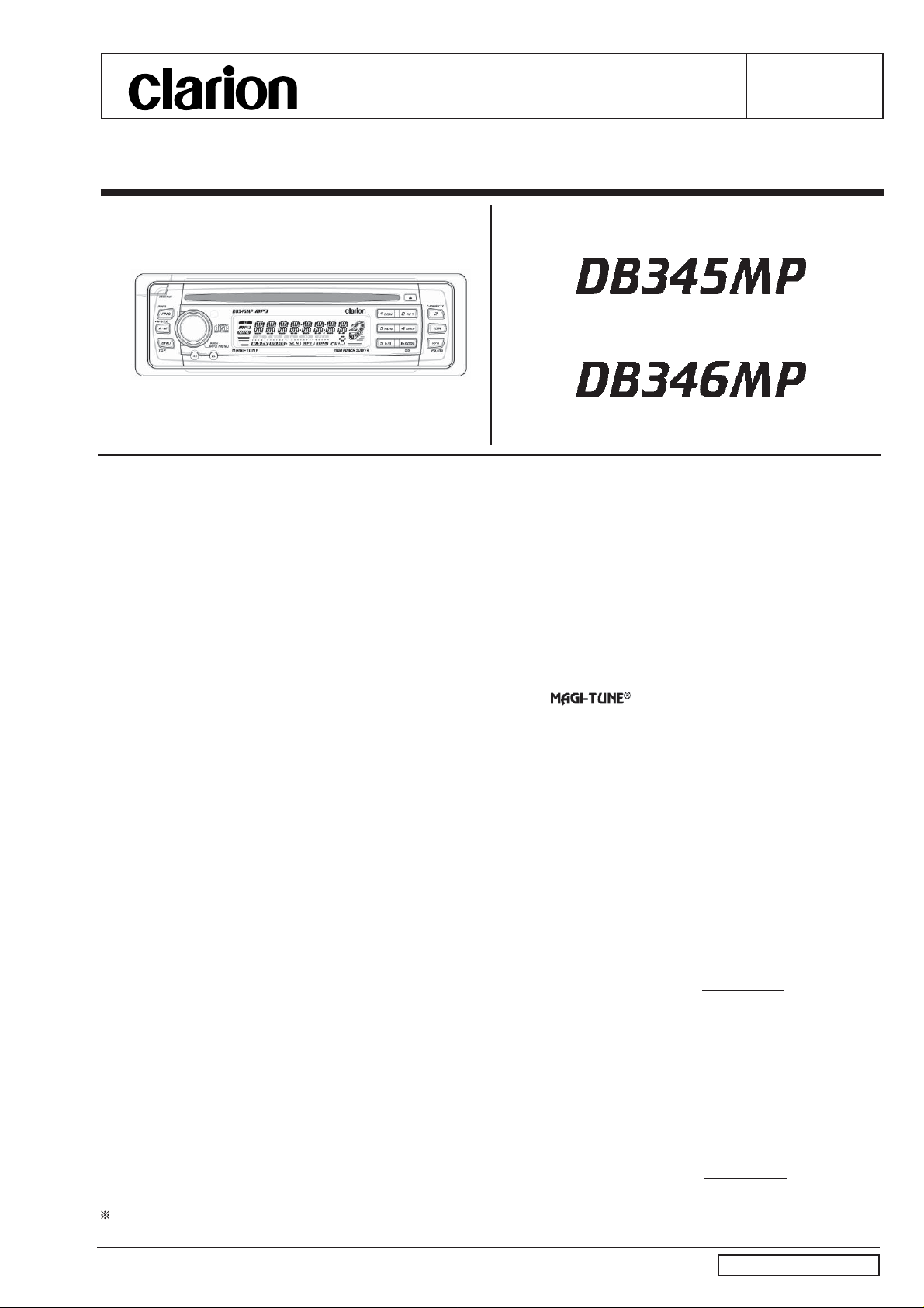
AM/FM CD/MP3 PlayerAM/FM CD/MP3 Player
AM/FM CD/MP3 Player
AM/FM CD/MP3 PlayerAM/FM CD/MP3 Player
ModelModel
Model
ModelModel
ice Manualice Manual
ice Manual
ice Manualice Manual
(PE-2640B-A: For U.S.A.)
ModelModel
Model
ModelModel
(PE-2640K-A: For other countries)
NOTE
1. We cannot supply PWB with component parts in
principle. When a circuit on PWB has failure, please repair it
by component parts base. Parts which are not mentioned
in service manual are not supplied.
FEATURES
1. Visible Blue Negative LCD and White Illuminated Buttons
2. Aluminium Detachable Faceplate
3. Rotary Volume for Easy Operation
4. Z-Enhancer with 3 Mode Sound Selector
5. MAGNA BASS EX for Dynamic Bass Tuning
6. FM Reception System
7. Seek/Manual Up/Down Tuning
8. 8-Times Oversampling Digital Filter and Dual 1-Bit
D/A Converters
9. Preset Station Scan (PS), Automatic Store (AS)
10. 4-Channel RCA Line Level Output
11. AM 1 band, FM 3 bands each 6 channels total 24
channels, Preset Memory Function
12. Repeat/Random Play/Intro Music Scan
13. 200W (50 W x 4) Maximum Power Output
14. IR Remote Control Included
15. MP3NAVI for Quick Music Folder and Track Search
16 MP3 File Playable with ID3-TAG Display
COMPONENTS
PE-2640B-A / PE-2640K-APE-2640B-A / PE-2640K-A
PE-2640B-A / PE-2640K-A
PE-2640B-A / PE-2640K-APE-2640B-A / PE-2640K-A
Source unit 1
Battery (SUM-3)
(PE-2640B only) 2
Remote Controller
(PE-2640B only) RCB-164-201 1
DCP Case 335-5734-05 1
Mounting bracket 300-7742-20 1
Escutcheon (Outer-Es)
(PE-2640B) 370-6100-00 1
(PE-2640K) 370-6096-00 1
Extension Lead 854-6391-60 1
Part’s bag 1
Removal key 331-2497-20 2
Stopper (PE-2640B only) 335-4899-20 1
- 1 -- 1 -
- 1 -
- 1 -- 1 -
DB345MP/DB346MPDB345MP/DB346MP
DB345MP/DB346MP
DB345MP/DB346MPDB345MP/DB346MP
Page 2
To engineers in charge of repair or
inspection of our products.
Before repair or inspection, make sure to follow the
instructions so that customers and Engineers in charge of
repair or inspection can avoid suffering any risk or injury.
1. Use specified parts.
The system uses parts with special safety features
against fire and voltage. Use only parts with equivalent
characteristics when replacing them.
The use of unspecified parts shall be regarded as remodeling for which we shall not be liable.The onus of
product liability (PL) shall not be our responsibility in
cases where an accident or failure is as a result of
unspecified parts being used.
2. Place the parts and wiring back in their original
positions after replacement or re-wiring.
For proper circuit construction, use of insulation tubes,
bonding, gaps to PWB, etc., is involved. The wiring connection and routing to the PWB are specially planned
using clamps to keep away from heated and high voltage parts. Ensure that they are placed back in their
original positions after repair or inspection.
If extended damage is caused due to negligence during repair, the legal responsibility shall be with the repairing company.
3. Check for safety after repair.
Check that the screws, parts and wires are put back
securely in their original position after repair. Ensure
for safety reasons there is no possibility of secondary
problems around the repaired spots.
If extended damage is caused due to negligence of repair, the legal responsibility shall be with the repairing
company.
4. Caution in removal and making wiring connection to
the parts for the automobile.
Disconnect the battery terminal after turning the ignition key off. If wrong wiring connections are made with
the battery connected, a short circuit and/or fire may
occur. If extensive damage is caused due to negligence
of repair, the legal responsibility shall be with the repairing company.
5. Cautions regarding chips.
Do not reuse removed chips even when no abnormality is observed in their appearance. Always replace them
with new ones. (The chip parts include resistors, capacitors, diodes, transistors, etc.). The negative pole of
tantalum capacitors is highly susceptible to heat, so
use special care when replacing them and check the
operation afterwards.
6. Cautions in handling flexible PWB.
Before working with a soldering iron, make sure that the
iron tip temperature is around 270°C. Take care not to
apply the iron tip repeatedly (more than three times) to the
same patterns. Also take care not to apply the tip with
force.
7. Turn the unit OFF during disassembly and parts replacement. Recheck all work before you apply power to the
unit.
8. Cautions in checking that the optical pickup lights up.
The laser is focused on the disc reflection surface
through the lens of the optical pickup. When checking
that the laser optical diode lights up, keep your eyes
more than 30cm away from the lens. Prolonged
viewing of the laser within 30cm may damage your
eyesight.
9. Cautions in handling the optical pickup
The laser diode of the optical pickup can be damaged
by electrostatic charge caused by your clothes and body.
Make sure to avoid electrostatic charges on your clothes
or body, or discharge static electricity before handling
the optical pickup.
9-1.Laser diode
The laser diode terminals are shorted for transportation
in order to prevent electrostatic damage. After
replacement, open the shorted circuit. When removing
the pickup from the mechanism, short the terminals by
soldering them to prevent this damage.
9-2.Actuator
The actuator has a powerful magnetic circuit. If a
magnetic material is put close to it. Its characteristics
will change. Ensure that no foreign substances enter
through the ventilation slots in the cover.
9-3.Cleaning the lens
Dust on the optical lens affects performance. To clean
the lens, apply a small amount of isopropyl alcohol to
lens paper and wipe the lens gently.
CAUTIONS
Use of controls, adjustments, or performance of procedures
other those specified herein, may result in hazardous
radiation exposure.
The compact disc player should not be adjustment or
repaired by anyone except properly qualified service
personnel.
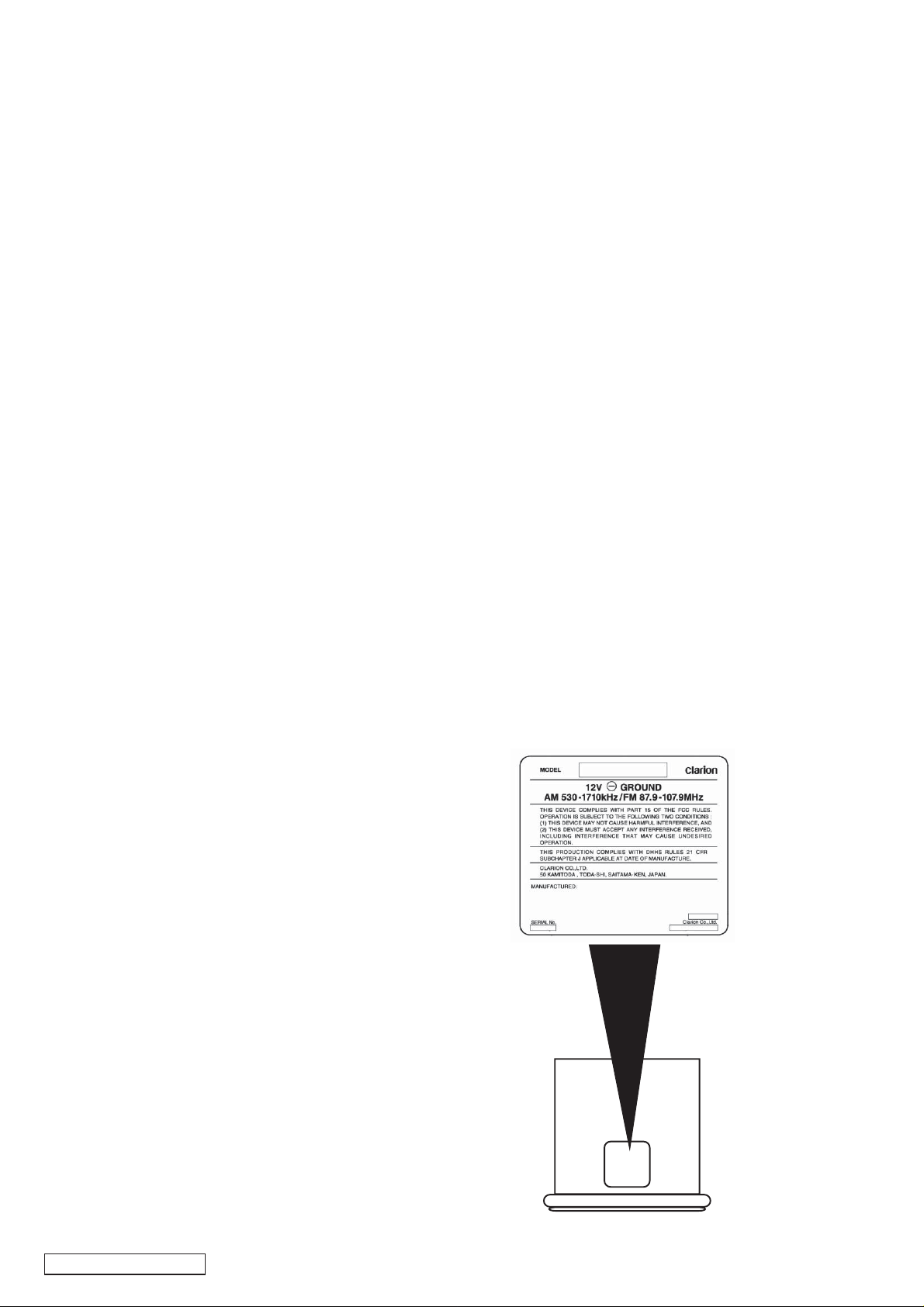
Bottom View of
Main Unit
DB345MP/DB346MPDB345MP/DB346MP
DB345MP/DB346MP
DB345MP/DB346MPDB345MP/DB346MP
- 2 -- 2 -
- 2 -
- 2 -- 2 -
Page 3
TROUBLESHOOTING
ProblemProblem
Problem
ProblemProblem
Power does not turn on.
(No sound is produced).
Compact disc cannot be
loaded.
Sound skips or is noisy.
Sound is bad directly after
power is turned on.
Nothing happens when buttons
are pressed.
Display is not accurate.
CauseCause
Cause
CauseCause
Fuse is blown. Replace with a fuse of the same amperage.
Incorrect wiring Read the attached “Installation/Wire connection
Guide” once again and wire properly.
Another compact disc is already
loaded.
Compact disc is dirty.
Compact disc is heavily scratched
or warped.
Water droplets may form on the
internal lens when the car is
parked in a humid place.
Microprocessor has
malfunctioned due to noise, etc.
Eject the compact disc before loading the new
one.
Clean the compact disc with a soft cloth.
Replace with a compact disc with no scratches.
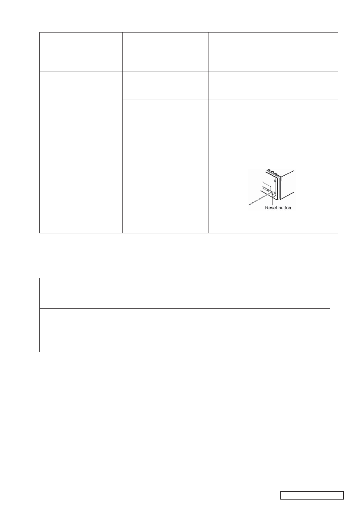
Let dry for about 1 hour with the power on.
Turn off the power, then press the
button and remove the DCP.
Press the reset button for about 2 seconds with a
thin rod.
MeasureMeasure
Measure
MeasureMeasure
[RELEASE][RELEASE]
[RELEASE]
[RELEASE][RELEASE]
DCP or main unit connectors are
dirty.
Wipe the dirt off with a soft cloth moistened with
cleaning alcohol.
ERROR DISPLAYS
To protect the system, this unit has been equipped with self diagnostic functions. If a fault arises, a warning is
issued by various error displays. Follow the corrective measures and remove the fault.
Error Display
ER2
ER3
ER6
This error display indicates that a fault has arised in the mechanism of the
source unit (for example, the disc cannot be ejected).
!Check the source unit
This error display indicates that the pickup focus is off because of a scratched
disc or some other factor during source unit play.
!Check the compact unit
This indicates that the CD’s TOC (table of contents) cannot be read, because
the selected disc is upside-down.
Corrective Measure
- 3 -- 3 -
- 3 -
- 3 -- 3 -
DB345MP/DB346MPDB345MP/DB346MP
DB345MP/DB346MP
DB345MP/DB346MPDB345MP/DB346MP
Page 4
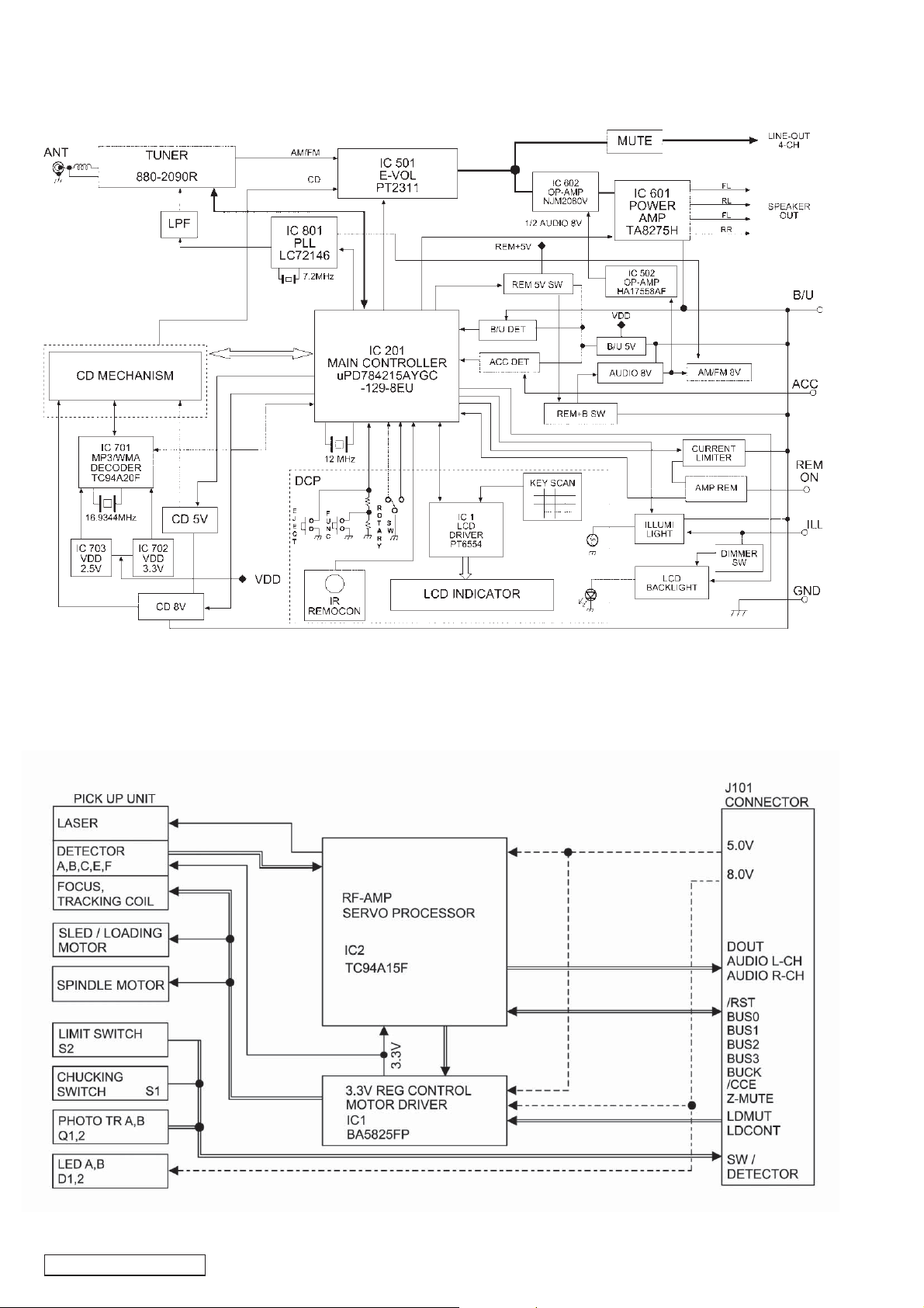
BLOCK DIAGRAM
MAIN UNIT SECTION
CD MECHANISM SECTION 929-0290-80
DB345MP/DB346MPDB345MP/DB346MP
DB345MP/DB346MP
DB345MP/DB346MPDB345MP/DB346MP
- 4 -- 4 -
- 4 -
- 4 -- 4 -
Page 5
EXPLANATION OF IC
uPD784215AYGC-129-8EU 052-3933-00
Master Micro computer
Outward FormOutward Form
Outward Form
Outward FormOutward Form
100 pins, plastic QFP
Terminal Description
1 VOL_CLK O E-VOL Control Clock output
2 VOL_DATA O E-VOL Control Data output
3 REM_DET I While protecting circuit motion, it
is at ‘HI’
4 OFFSET DET I While Power Amp IC is abnormal,
it is at ‘LOW’
5 PHONE_INT I NC
6NC -NC
7 MP3 REQ I REQ input from MP3 decoder
8NC -NC
9 V DD - Power supply terminal 5V
10 X_OUT - Crystal 12MHz (Main system
clock)
11 X_IN - Crystal 12MHz (Main system
clock)
12 VSS - GND
13 XT_OUT - NC
14 XT_IN - GND
15 RES ET - Reset port (When system is
reset, it is at ‘LOW’)
16 NC - NC
17 B/U DET I B/U detecting terminal
18 ACC DET I ACC detecting terminal
19 REMOCON I IR Sensor signal input for Remote
Control
20 KEY_INT I When this terminal turns low, key
A/D terminal detects the key
pushed (FNC, EJECT & DCP
keys)
21 SBSY I GS1-MC CD Sub-code block
sync detection input
22 TBASE I PLL Time Base signal input (8Hz)
23 AVDD - Analog Power supply 5V
24 AVREF0 - ADC Reference Voltage Input
25 KEY A/D I FNC/EJECT/DCP detection
terminal for A/D converter
26 TEST I TEST keys detection terminal
(For Test Mode purpose)
27 NC - NC
28 NC - NC
29 NC - NC
30 NC - NC
31 NC - NC
32 NC - NC
33 AVSS - Analog GND
Pin No PIN NAME I/O DESCRIPTIONPin No PIN NAME I/O DESCRIPTION
34 NC - NC
35 NC - NC
36 AVREF1 - DAC Reference Voltage Input
37 NC - NC
38 NC - NC
39 NC - NC
40 NC - NC
41 NC - NC
42 NC - NC
43 NC - NC
44 NC - NC
45 MP3 SDA I/O MP3 Data Communication Port
(I2C bus)
46 NC - NC
47 MP3 SCL O MP3 Clock Output (I2C bus)
48 MP3 RESET O When MP3 decoder is reset, it is
at ‘LOW’
49 MP3 STANDBY O When MP3 decoder is at standby
mode, it is at ‘LOW’
50 STANDBY O Power Amp IC control terminal
51 REM_ON O While Power on, it is at ‘HI’
52 CD_8V_REM O CD power supply control terminal
+8V
53 B/L + B O Illumination Control Output (While
ACC is ON, it is at ‘HI’)
54 C S1 I Destination Selection Input. Refer
Table 1.
55 C S2 I Destination Selection Input. Refer
Table 1.
56 LCD SI I Serial data input communication
line to LCD Control IC
57 LCD SO O Serial data output communication
line to LCD Control IC
58 LCD SCK O Serial clock output communication
line to LCD Control IC
59 LCD CE O LCD chip enable output
60 VOL-CW I Use for rotary volume
61 VOL-CCW I Use for rotary volume
62 NC - NC
63 NC - NC
64 NC - NC
65 TR-B I GS1-MC CD Disc Detection Input
(HI: with disc, LOW: without disc)
- 5 -- 5 -
- 5 -
- 5 -- 5 -
DB345MP/DB346MPDB345MP/DB346MP
DB345MP/DB346MP
DB345MP/DB346MPDB345MP/DB346MP
Page 6
66 S-STOP I GS1-MC CD Pick-up Inner Limit
Detection Input (HI: Limit, LOW:
Playable)
67 RST O GS1-MC CD Servo Reset Output
(While reset, it is at ‘LOW’)
68 BUCK O GS1-MC CD Servo Clock Output
69 Z-MUTE I GS1-MC CD DAC Zero Data
Detection Input (While Zero data
is detected, it is at ‘HI’)
70 D_OUT I NC
71 CCE O GS1-MC CD Servo Chip Enable
Output
72 VSS - GND
73 BUS3 I/O GS1-MC CD Servo Data
Communication Port
74 BUS2 I/O GS1-MC CD Servo Data
Communication Port
75 BUS1 I/O GS1-MC CD Servo Data
Communication Port
76 BUS0 I/O GS1-MC CD Servo Data
Communication Port
77 CHU-SW I GS1-MC CD Disc Chucking
Detection Input (HI: Chuck
uncompleted, LOW: Chuck
completed)
78 TR-A I GS1-MC CD 8cm Disc Detection
Input (HI: 12cm disc, LOW: 8cm
disc)
79 LD_MUTE O GS1-MC CD Sled Motor Standby
Output (HI: Operation, LOW:
Standby)
80 LD_COUNT O GS1-MC CD Loading/Eject
Control Output (HI: Eject, LOW:
Loading)
Pin No PIN NAME I/O DESCRIPTIONPin No PIN NAME I/O DESCRIPTION
81 VDD - Power supply terminal 5V
82 PLL DI I PLL Data Input
83 PLL DO O PLL Data Output
84 PLL CLK O PLL Clock
85 PLL CE O PLL Chip Enable
86 NC - NC
87 NC - NC
88 NC - NC
89 NC - NC
90 NC - NC
91 SD/ST_IND I AM/FM SD and Stereo Detection
Signal Input (HI: SD Off/Mono,
LOW: SD On/Stereo)
92 NC - NC
93 NC - NC
94 TEST/VPP - NC
95 REM 5V O System 5V power supply control
terminal
96 SYS_MUTE O Audio Mute Control Output (While
mute is ON, it is at ‘LOW’)
97 CD_5V_REM O CD power supply control terminal
+5V
98 NC - NC
99 NC - NC
100 NC - NC
TABLE 1.TABLE 1.
TABLE 1. The Destination Setting Terminal
TABLE 1.TABLE 1.
U.S. Area Setting Outside U.S. Area Setting
CS1 (Pin 54) L H
CS2 (Pin 55) L L
DB345MP/DB346MPDB345MP/DB346MP
DB345MP/DB346MP
DB345MP/DB346MPDB345MP/DB346MP
- 6 -- 6 -
- 6 -
- 6 -- 6 -
Page 7
TC94A15F 051-6399-00
CD Mechanism IC
Outward FormOutward Form
Outward Form
Outward FormOutward Form
100 pins, plastic QFP
Terminal Description
1 IPF OUT O IP flag output
2 SB OK O O Sub code Q data CRCC OK
signal output
3 CLOCKIO I/O The clock pulse input/output for
the sub code reading
4 VDD - Positive supply voltage
5 VSS - Nagative supply voltage
6DATA ODATA
7 S F SY O O Playback frame synchronous
signal output
8 SB SY O O Sub code block sychronous
signal output
9 H S O O The play speed flag ouput
10 UHSO O The play speed flag output
11 AR SEL IN I Fix to the high level
12 AWRC O The control signal ouput for the
active wide range VCO
13 P VDD - PLL positive supply voltage.
14 P DO O Phase difference signal output of
EFMPLCK.
15 TMAX S O T max judgment output.
16 TMAX O T max judgment output.
17 LPF N I Inverted input of LPF for PLL.
18 LPF OUT O The output terminal for the Low
Pass Filter.
19 P Vref - PLL reference voltage.
20 VCO FILTER O Loop filter for VCO.
21 VCO Ref I VCO reference voltage input.
22 DTC N O For the analog slicer.
23 DTC P O For the analog slicer.
24 PLL VSS - PLL ground.
25 SLCO O Output of internal DAC for data
slice level generation.
26 RF IN I RF signal input.
27 RF RP I RF ripple input.
28 RF EQ OUT O The output of the RF equalizer.
29 A VDD - Positive supply voltage for the
Analog section.
30 RES IN - For reference current setting.
31 Vref OUT O The reference voltage output.
32 VMDIR O The reference voltage output.
33 TESTR O The compensation terminal for
RFEQO offset.
34 INVSEL I MDI polarity selection.
35 AGCI I The input terminal of RF AGC
amplifier.
36 RF DCI I The input terminal for RF peak
detection.
37 RF OUT O RF signal output.
Pin No PIN NAME I/O DESCRIPTIONPin No PIN NAME I/O DESCRIPTION
38 PN SEL I The transistor type selection
input for laser diode driver.
L=NPN, H=PNP.
39 EQ SET O The equalizer setting terminal.
40 RF VDD - RF power supply.
41 L DO O The laser diode drive output.
42 MDI I Monitor photo diode signal input.
43 RF VSS - RF ground.
44 FNI 2 I Main beam signal input.
45 FNI 1 I Main beam signal input.
46 FPI 2 I Main beam signal input.
47 FPI 1 I Main beam signal input.
48 TPI I Sub beam signal input.
49 TNI I Sub beam signal input.
50 FTEO O For test.
51 RF ZI I RF ripple zero cross signal input.
52 A VS S - Analog ground.
53 RF RP O RF ripple signal output.
54 RF DC O RF peak detection signal output.
(hologram suitable)
55 FE I O Focus error signal output.
56 SBAD O Sub beam add signal output.
57 TEI O Tracking error signal output.
58 TE Z IN I Tracking error signal inpur for
zero cross.
59 A VDD - Positive supply voltage for the
Analog section.
60 F OO O Focus equalizer output.
61 TR O O Tracking equalizer output.
62 Vref O Reference voltage output.
63 FMO O Field equalizer output / Speed
error output.
64 DM O O Disk equalizer output.
65 IO2A I/ O General input/output.
66 IO3A I/ O General input/output.
67 MON I T O Internal DSP signal monitor.
68 FG IN I FG input for the spindle CAV
servo.
69 VSS - Negative supply voltage.
70 VDD - Positive supply voltage.
71 TES IN I For test.
72 X VSS - Master clock analog ground.
73 X I N I Crystal connection.
74 X O O Crystal connection.
75 X VDD - Clock power supply.
76 D VS S - Digital ground.
- 7 -- 7 -
- 7 -
- 7 -- 7 -
DB345MP/DB346MPDB345MP/DB346MP
DB345MP/DB346MP
DB345MP/DB346MPDB345MP/DB346MP
Page 8

77 RO O Right channel data output for 1-bit
DAC.
78 D VDD - Positive supply voltage for the
digital section.
79 D Vref O Digital reference voltage.
80 LO O Left channel data output for 1-bit
DAC.
81 D VSS - Digital ground.
82 Z DET O O 1bit DAC zero flag output.
83 VSS - Negative supply voltage.
84 BUS 0 I/O CD IC Data input / output.
85 BUS 1 I/O CD IC Data input / output.
86 BUS 2 I/O CD IC Data input / output.
87 BUS 3 I/O CD IC Data input / output.
88 BU CK IN I CD IC Data clock input.
89 CCEI I Chip enable input.
TC94A20F 051-6704-00
MP3 Decorder IC
Pin No PIN NAME I/O DESCRIPTIONPin No PIN NAME I/O DESCRIPTION
90 RSTI I Reset signal input.
91 VDD - Positive supply voltage.
92 EMPHI/FAO I /O Emphasis input for 1-bit DAC /
Flag A output.
93 BCKI/FBO I/O Bit clock input for 1-bit DAC / Flag
B output.
94 AIN/FCO I/O Audio input for 1-bit DAC / Flag C
output.
95 LRCKI/FDO I/O LR clock input for 1-bit DAC /
Flag D output.
96 EMPHO O Emphasis flag output.
H=Emphasis ON.
97 B CK O O Bit clock output.
98 A OUT O Audio signal output.
99 LR CK O O LR clock output.
100 D OUT O Serial data output.
Outward FormOutward Form
Outward Form
Outward FormOutward Form
64 pins, plastic QFP
Terminal Description
1 RESET I Reset Port
2 MiMD I Mode selection (H:I²C L:Serial)
3 MiCS I NC
4 MiLP I NC
5 MiDi o I/ O Data input and output for
micom Interface (I²C:SDA)
6 MiCK I Clock input for micom interface
(I²C:SCL)
7 MiACK O NC
8 VDDT - VDD 3.3V
9 SDo O Data output
10 BCKo O NC
11 LRCKo O NC
12 SDi0 I Data Input-0
13 BCKiA I Bit Clock Input-A
14 LRCKiA I LR Clock Input-A
15 SDi1 I NC
16 BCKiB I NC
17 LRCKiB I NC
18 VD D - VDD 2.5V
19 STANDBY I Control input for Stand-by
mode (H:STBY L:Normal)
20 VSS - GND
21 VSSL - GND
22 VRAL - NC
23 LO O NC
24 VDAL - VDD 2.5V
25 VDAR - VDD 2.5V
26 RO O NC
27 VRAR - N C
28 VSSR - GND
29 TESTP I GN D
30 TXO O NC
31 Po0 O NC
Pin No PIN NAME I/O DESCRIPTIONPin No PIN NAME I/O DESCRIPTION
32 Po1 O NC
33 Po2 O NC
34 Po3 O NC
35 VDDT - VDD 3.3V
36 Po4 O NC
37 Po5 O NC
38 Po6 O NC
39 Po7 O Request pin for interrupt host
40 VSS - GND
41 REQ I/O NC
42 VDDM - VDD 2.5V
43 Fi0 I N C
44 Fi1 I N C
45 VSSM - GND
46 Pi0 I NC
47 Pi1 I NC
48 VSS - GND
49 Pi2 I NC
50 Pi3 I NC
51 Pi4 I NC
52 VD D - VDD 2.5V
53 Pi5 O NC
54 TSTiN I NC
55 Fi2 I N C
56 VSSP - GND
57 Pdo O Phase detector output
58 Vcoi I Controlled voltage input for VCO
circuit
59 VDDP - VDD 2.5V
60 CKi I/O NC
61 VDDX - VDD 2.5V
62 Xi I X-TAL 16.9344MHz
63 Xo O X-TAL 16.9344MHz
64 VSSX - GND
DB345MP/DB346MPDB345MP/DB346MP
DB345MP/DB346MP
DB345MP/DB346MPDB345MP/DB346MP
- 8 -- 8 -
- 8 -
- 8 -- 8 -
Page 9

EXPLODED VIEW • PART LIST
Main Section/DCP Section
- 9 -- 9 -
- 9 -
- 9 -- 9 -
DB345MP/DB346MPDB345MP/DB346MP
DB345MP/DB346MP
DB345MP/DB346MPDB345MP/DB346MP
Page 10

NO . PART NO. DESCRIPTION Q'TY
1 DCP-465-600 DCP ASSY (PE-2640B-A) 1
DCP-472-800 DCP ASSY (PE-2640K-A) 1
1-1 716-0872-03 SCREW (PE-2640B-A) 2
716-0872-00 SCREW (PE-2640K-A) 2
1-2 371-5770-00
371-5770-01
1-3 371-5771-00 FACE PLATE (L)(PE-2640B-A) 1
371-5771-01 FACE PLATE (L)(PE-2640K-A) 1
1-4 382-6923-00
382-6924-00
1-5 750-6747-00 SPRING 1
1-6 382-6925-00 BUTTON ASSY (R) 1
1-7 335-7140-00 ILLUMI PLATE (R) 1
1-8 347-7208-00 STICKER 2
1-9 382-6926-00 BUTTON ASSY (L) 1
1-10 382-6924-00 ILLUMI PLATE (L) 1
1-11 335-7139-00 REAR COVER 1
1-12 716-0872-11 SP SCREW (M1.7 X 6) 4
1-13 331-3749-00 LCD COVER 1
1-14 379-1278-41 INDICATOR (LCD) 1
1-15 347-7092-00 FILM 1
1-16 347-7093-00 SHADE 1
1-17 335-7190-00 LCD ILLUMI 1
1-18 001-7046-00 DIODE 1
1-19 335-7192-00 LCD HOLDER 1
1-20 016-9900-92 VR W/SHAFT 1
1-21 345-7148-20 LAMP CAP 4
1-22 017-0410-00 PILOT LAMP (14V 40mA) 4
1-23 013-6005-51 TACT SWITCH 12
1-24 013-6305-50 TACT SWITCH 3
1-25 060-4008-00 IR-RECEIVER 1
1-26 347-7026-00 BLACK MATTEE STICKER 1
1-27 076-0703-12 PLUG 1
1-28 051-6013-50 IC 1
1-29 -------------------- MAIN PWB (SWITCH) 1
1-30 947-0544-60 ES-DIAL-ASSY(PE-2640B-A) 1
947-0545-60 ES-DIAL-ASSY(PE-2640K-A) 1
1-31 947-0543-60 VOL-KNOB-ASSY 1
2 346-0097-00 LEATHER SHEET 1
3 714-2606-87 MC SCREW (M2.6 X 6) 2
4 370-6101-00 INNER ESC 1
5 382-4078-20 BUTTON P-UP 1
6 750-3173-00 SPRING 2
FACE PLATE(R)(PE-2640B-A)
FACE PLATE(R)(PE-2640K-A)
RELEASE BUTTON (PE-2640B-A)
RELEASE BUTTON (PE-2640K-A) 1
1
1
1
NO . PART NO. DESCRIPTION Q'TY
7 331-3609-00 HOOK PLATE 1
8 716-0778-00 WAVE SCREW (2 X 6) 2
9 335-5915-20 HOOK 1
10 341-1627-20 SHAFT 1
11 750-3219-20 SPRING 1
12 074-1237-76 OUTLET SOCKET 1
13 074-1316-12 OUTLET SOCKET (DCP) 1
14 816-2640-60 FLAT WIRE 1
15 331-3630-00 CONNECTOR COVER 1
16 013-3932-01 TACT SWITCH 1
17 880-2090R TUNER 1
18 331-1861-21 EARTH PLATE 1
1 9 -------------------- MAIN PWB 1
20 076-0349-04 CONNECTOR 1
21 854-4569-60 EXTENSION LEAD 1
22 313-1873-00 HEAT SINK 1
23 331-3631-00 RCA BRKT 1
24 075-0388-00 RCA JACK 1
25 074-1214-00 OUTLET SOCKET 1
26 009-9006-60 CHOKE 1
27 331-3367-01 IC HOLDER 1
28 051-2042-00 POWER IC 1
29 092-4000-51 ANT-RECEPT 1
30 313-1872-05 HEAT SINK 1
31 855-8000-08 RCA PIN CORD 1
32 345-3799-0L RUBBER PART 2
33 331-3637-00 BRACKET 1
34 716-1753-10 SCREW (M3 X 6) 1
35 335-0833-01 CABLE TIE 1
36 714-2012-81 MC SCREW (M2 X 12) 1
37 731-3008-80 TAPTIGHT (M3 X 8) 4
38 714-3006-81 TAPTIGHT (M3 X 6) 2
39 731-3012-80 TAPTIGHT (M3 X 12) 2
40 286-6310-00 SET PLATE (PE-2640B-A) 1
286-6311-00 SET PLATE (PE-2640K-A) 1
41 311-1848-00 LOWER CASE 1
42 310-1775-05 UPPER CASE 1
43 731-3005-81 TAPTIGHT (M3 X 5) 3
44 331-3607-00 MECHA BRACKET 2
45 714-2604-81 MC SCREW (M2.6 X 4) 3
46 929-0290-80 CD MECHA 1
47 331-3366-00 MECHA BRACKET 1
DB345MP/DB346MPDB345MP/DB346MP
DB345MP/DB346MP
DB345MP/DB346MPDB345MP/DB346MP
- 10 -- 10 -
- 10 -
- 10 -- 10 -
Page 11

EXPLODED VIEW • PARTS LIST
CD mechanism section 929-0290-80
- 11 -- 11 -
- 11 -
- 11 -- 11 -
DB345MP/DB346MPDB345MP/DB346MP
DB345MP/DB346MP
DB345MP/DB346MPDB345MP/DB346MP
Page 12

1 966-0595-25 DRIVE PLATE ASSY 1
2 969-0065-31 PICK UP UNIT 1
3 ————— LED PWB 1
4 ————— CD PWB 1
5 SMA-182-100 MOTOR ASSY(SPINDLE) 1
6 SMA-183-100 MOTOR ASSY(SLED) 1
7 HBS-524-100 CLAMPER SUB ASSY 1
7-1 620-1022-25 CLAMPER LINK 1
7-2 620-1023-23 CLAMPER PLATE 1
7-3 620-1024-23 SENSOR ARM 1
7-4 621-0708-20 CLAMPER RING 1
7-5 621-0626-21 STOPPER LINK 1
7-6 621-0627-21 DISC STOPPER 1
7-7 750-3471-20 SENSOR SPRING 1
8 803-4906-60 VINYL COAT WIRE(ORG) 1
9 816-2591-00 LEAD WIRE(YEL) 1
10 620-1025-22 ID-LOCK PLATE 1
11 620-1026-21 SPRING PLATE 1
12 620-1027-27 LOWER CHASSIS 1
13 620-1028-23 UPPER CHASSIS 1
14 966-0638-20 SH-RACK ASSY 1
15 621-0598-27 UPPER GUIDE 1
16 621-0599-26 ROLLER GUIDE 1
17 621-0600-26 SHIFT LEVER 1
18 621-0601-21 RACK 1
19 621-0602-22 LOCK ARM L 1
20 621-0603-25 LOCK ARM R 1
21 621-0724-21 GEAR BASE 1
22 621-0605-22 GEAR COVER 1
23 621-0723-20 IDLE CASE 1
24 816-2590-00 VINYL COAT WIRE(GRN) 1
25 621-0608-21 SECOND GEAR 1
26 621-0609-20 BASE GEAR 1
27 621-0610-20 IDLE GEAR A 1
28 621-0611-20 IDLE GEAR B 1
29 621-0612-21 ROLLER GEAR A 1
30 621-0719-20 ROLLER GEAR B 1
NO . PART NO. DESCRIPTION Q'TYNO . PART NO. DESCRIPTION Q'TY
31 621-0720-20 ROLLER GEAR C 1
32 621-0721-20 ROLLER GEAR D 1
33 621-0616-20 POWER GEAR A 1
34 621-0617-20 POWER GEAR B 1
35 621-0618-20 POWER GEAR C 1
36 621-0619-20 POWER GEAR D 1
37 621-0620-20 THREAD GEAR A 1
38 621-0621-20 THREAD GEAR B 1
39 621-0622-21 ROLLER SLEEVE 2
40 621-0623-23 LS-HOLDER 1
41 621-0624-22 GUIDE RAIL 1
42 816-2593-00 LE AD WI RE(P UR) 1
43 816-2542-01 FLAT WIRE(10P) 1
44 716-3473-00 SCREW (M2 X 3) 2
45 621-0709-20 SH-BASE 1
46 621-0629-20 LOADING ROLLER 2
47 345-8704-20 CUSHION RUBBER 1
48 622-1571-21 ROLLER SHAFT 1
49 624-0018-01 LEAD SCREW 1
50 629-0081-20 DAMPER F 2
51 629-0082-20 DAMPER R 1
52 714-2003-81 MACHINE SCREW (M2 X 3) 2
53 716-1507-00 SCREW (M2 X 3) 9
54 716-1733-00 SCREW (M1.7 X 2.3) 2
55 716-3469-00 S CREW (3 X 4) 2
56 716-3446-00 SCREW (M1.4 X 2.5) 2
57 750-3465-21 ROLLER SPRING L 1
58 750-3466-20 ROLLER SPRING R 1
59 750-3467-21 SHIFT SPRING 1
60 750-3468-20 RACK SPRING 1
61 750-3469-20 CLAMPER SPRING 1
62 750-3470-20 ID-LOCK SPRING 1
63 816-2592-00 LEAD WIRE(BLU) 1
64 750-3472-21 DR-SPRING F 2
65 750-3473-20 DR-SPRING RA 1
66 750-3474-20 DR-SPRING RB 1
67 750-3475-21 DR-SPRING C 1
DB345MP/DB346MPDB345MP/DB346MP
DB345MP/DB346MP
DB345MP/DB346MPDB345MP/DB346MP
- 12 -- 12 -
- 12 -
- 12 -- 12 -
Page 13

ELECTRICAL PARTS LIST
Main PWB Section (B1)
Note:- Several different parts of the same reference number are alternative parts.
Remarks:- #: For PE-2640B-A only @: For PE-2640K-A only
One of those parts is used in the set.
REF No. PART No. DESCRIPTION
ANT101 092-4000-51 ANT-RECEPT
BL101 880-2090R TUNER
C101 166-2201-50 50V 22pF
C102 166-2201-50 50V 22pF
C103 168-1032-55 50V 0.01uF
C104 168-1032-55 50V 0.01uF
C105 168-1032-55 50V 0.01uF
C106 187-1073-25 10V 100uF
C107 168-1045-56 25V 0.1uF
C108 168-1032-55 50V 0.01uF
C109 187-4763-35 16V 47uF
C110 187-1073-25 10V 100uF
C111 168-1032-55 50V 0.01uF
C112 168-6822-55 50V 6800pF
C113 168-2732-55 50V 0.027uF
C114 168-2732-55 50V 0.027uF
C115 168-1022-55 50V 1000pF
C116 168-4732-78 50V 0.047uF
C117 187-1053-65 50V 1uF
C118 168-1232-55 50V 0.012uF
C126 166-1011-50 50V 100pF
C127 168-1045-56 25V 0.1uF
C128 168-1032-55 50V 0.01uF
C129 168-1045-56 25V 0.1uF
C201 042-1598-90 10V 470uF
C202 168-6832-78 50V 0.068uF
C203 166-1501-50 50V 15pF
C204 166-1501-50 50V 15pF
C206 168-1532-55 50V 0.015uF
C207 168-6832-78 50V 0.068uF
C208 042-1598-90 10V 470uF
C209 178-2242-78 25V 0.22uF
C210 168-1032-55 50V 0.01uF
C211 168-1032-55 50V 0.01uF
C212 168-1032-55 50V 0.01uF
C213 168-1032-55 50V 0.01uF
C215 168-1032-55 50V 0.01uF
C216 168-1032-55 50V 0.01uF
C401 168-2232-55 50V 0.022uF
C402 168-1022-55 50V 1000pF
C405 168-1032-55 50V 0.01uF
C406 168-1045-56 25V 0.1uF
C501 187-2253-65 50V 2.2uF
C502 187-2253-65 50V 2.2uF
C503 187-2253-65 50V 2.2uF
C504 178-4742-78 25V 0.47uF
C505 168-1045-56 25V 0.1uF
C506 168-1045-56 25V 0.1uF
C507 168-2722-55 50V 2700pF
C508 168-1032-55 50V 0.01uF
C510 168-2222-55 50V 2200pF
C511 187-2253-65 50V 2.2uF
C512 187-2253-65 50V 2.2uF
C513 187-2253-65 50V 2.2uF
REF No. PART No. DESCRIPTION REF No. PART No. DESCRIPTION
C514 178-4742-78 25V 0.47uF
C515 168-1045-56 25V 0.1uF
C516 168-1045-56 25V 0.1uF
C517 168-2722-55 50V 2700pF
C518 168-1032-55 50V 0.01uF
C520 168-2222-55 50V 2200pF
C521 187-2263-35 16V 22uF
C523 187-1073-15 6.3V 100uF
C524 187-1063-35 16V 10uF
C530 168-1032-55 50V 0.01uF
C531 166-1011-50 50V 100pF
C532 166-1011-50 50V 100pF
C533 166-1011-50 50V 100pF
C534 166-1011-50 50V 100pF
C535 166-1011-50 50V 100pF
C537 166-1011-50 50V 100pF
C538 168-1022-55 50V 1000pF
C539 166-1011-50 50V 100pF
C551 187-1063-35 16V 10uF
C552 166-4711-50 50V 470pF
C553 187-1063-35 16V 10uF
C554 166-4711-50 50V 470pF
C581 187-1063-35 16V 10uF
C582 166-4711-50 50V 470pF
C583 187-1063-35 16V 10uF
C584 166-4711-50 50V 470pF
C602 178-3932-78 25V 0.039uF
C603 178-3932-78 25V 0.039uF
C612 178-3932-78 25V 0.039uF
C613 178-3932-78 25V 0.039uF
C622 187-1063-35 16V 10uF
C623 178-4742-78 25V 0.47uF
C624 187-1053-65 50V 1uF
C625 168-2222-55 50V 2200pF
C626 168-2222-55 50V 2200pF
C627 168-2222-55 50V 2200pF
C628 168-2222-55 50V 2200pF
C629 168-2222-55 50V 2200pF
C630 168-2222-55 50V 2200pF
C631 168-2222-55 50V 2200pF
C632 168-2222-55 50V 2200pF
C641 168-1542-55 25V 0.15uF
C642 168-1542-55 25V 0.15uF
C643 168-1542-55 25V 0.15uF
C644 166-2201-50 50V 22pF
C645 166-2201-50 50V 22pF
C646 168-1542-55 25V 0.15uF
C647 166-2201-50 50V 22pF
C648 168-1542-55 25V 0.15uF
C649 168-1542-55 25V 0.15uF
C650 166-2201-50 50V 22pF
C651 168-1542-55 25V 0.15uF
C652 168-1542-55 25V 0.15uF
C701 168-1045-56 25V 0.1uF
C702 168-1045-56 25V 0.1uF
C703 168-1045-56 25V 0.1uF
C706 168-1045-56 25V 0.1uF
C707 168-1045-56 25V 0.1uF
C715 168-1045-56 25V 0.1uF
C716 168-1045-56 25V 0.1uF
C717 168-1045-56 25V 0.1uF
C718 168-1045-56 25V 0.1uF
C719 187-3343-65 50V 0.33uF
C720 168-1045-56 25V 0.1uF
C721 168-1045-56 25V 0.1uF
C722 187-4763-15 6.3V 47uF
C723 187-1063-35 16V 10uF
C724 166-2001-50 50V 20pF
C725 166-2001-50 50V 20pF
C726 168-1045-56 25V 0.1uF
C727 178-1052-78 16V 1uF
C728 168-1032-55 50V 0.01uF
C729 187-1063-35 16V 10uF
C730 178-1052-78 16V 1uF
C731 168-1032-55 50V 0.01uF
C732 187-2273-15 6.3V 220uF
C736 168-2222-55 50V 2200pF
C737 168-1045-56 25V 0.1uF
C801 166-1011-50 50V 100pF
C802 166-3311-50 50V 330pF
C803 166-1011-50 50V 100pF
C804 166-1011-50 50V 100pF
C805 166-1011-50 50V 100pF
C806 187-4763-15 6.3V 47uF
C807 168-1032-55 50V 0.01uF
C808 187-1053-65 50V 1uF
C809 168-1045-56 25V 0.1uF
C810 166-1501-50 50V 15pF
C811 166-1801-50 50V 18pF
C812 168-1022-55 50V 1000pF
C901 189-2283-32 16V 2200uF
C902 172-1041-15 50V 0.1uF
C903 187-1063-35 16V 10uF
C904 042-1598-90 10V 470uF
C905 187-2263-35 16V 22uF
C906 042-1598-90 10V 470uF
C907 187-1073-25 10V 100uF
C908 042-1452-81 10V 220uF
C910 042-1598-90 10V 470uF
C911 168-4732-78 50V 0.047uF
C914 168-1032-55 50V 0.01uF
C915 187-1063-35 16V 10uF
C927 042-1598-90 10V 470uF
C929 168-1045-56 25V 0.1uF
CCT201 050-0148-50 CCT 1K ohm
CCT202 050-0148-50 CCT 1K ohm
CCT203 050-0148-50 CCT 1K ohm
CCT204 050-0148-50 CCT 1K ohm
DB345MP/DB346MPDB345MP/DB346MP
DB345MP/DB346MP
DB345MP/DB346MPDB345MP/DB346MP
- 13 -- 13 -
- 13 -
- 13 -- 13 -
Page 14

REF No. PART No. DESCRIPTION
CCT207 050-0148-50 CCT 1K ohm
CCT208 050-0148-50 CCT 1K ohm
CCT209 050-0148-50 CCT 1K ohm
CCT210 050-0148-50 CCT 1K ohm
CCT211 050-0148-50 CCT 1K ohm
CCT212 050-0148-50 CCT 1K ohm
CCT213 050-0148-50 CCT 1K ohm
CCT214 050-0148-50 CCT 1K ohm
CCT215 050-0148-50 CCT 1K ohm
CCT216 050-0148-50 CCT 1K ohm
CCT217 050-0148-50 CCT 1K ohm
CCT218 050-0148-50 CCT 1K ohm
D201 001-0529-35 MA8062M
D601 001-0466-90 S5688B
D602 001-0466-90 S5688B
D603 001-0466-90 S5688B
D604 001-0466-90 S5688B
D605 001-0466-90 S5688B
D606 001-0466-90 S5688B
D607 001-0466-90 S5688B
D608 001-0466-90 S5688B
D609 001-1310-00 KDS160
D901 001-0592-00 RM4Z
D902 001-1310-00 KDS160
D903 001-0466-91 S5688G
D904 001-0330-90 1SS119
D905 001-0347-45 MA4082H
D906 001-0529-32 MA8056M
D907 001-0347-48 MA4091H
D908 001-0330-90 1SS119
D910 001-0347-32 MA4056M
D911 001-0330-90 1SS119
D912 001-0330-90 1SS119
D915 001-1310-00 KDS160
D916 001-1310-00 KDS160
D917 001-1310-00 KDS160
D918 001-0529-32 MA8056M
D920 001-0347-46 MA4091L
D925 001-0330-90 1SS119
D926 001-1310-00 KDS160
IC201 052-3933-00 uPD784215AYGC
-129-8EU
IC202 051-5413-09 S-80824KNUA
IC401 051-0869-58 NJM2103M
IC501 051-5033-90 PTC2311
IC502 051-3049-90 HA17558AF
IC601 051-2042-00 TA8275H
IC602 051-3019-90 NJM2060V
IC701 051-6704-00 TA94A20F
IC702 051-3327-90 TAR5S33
IC703 051-3326-90 TAR5S25
IC801 051-6201-90 LC72146M
J201 074-1316-12 12P
J501 074-1237-76 26P
REF No. PART No. DESCRIPTION REF No. PART No. DESCRIPTION
J701 076-0349-04 4P
J901 074-1214-00 16P
L101 010-2003-04 COIL
L103 010-2330-67 5.6uH
L201 010-2330-62 2.2uH
L801 010-2330-86 220uH
Q101 125-2199-93 KRC103S
Q102 125-0199-98 KRA118S
Q103 125-0199-93 KRA103S
Q401 125-2199-93 KRC103S
Q521 125-0199-92 KRA102S
Q551 125-4010-90 KTC 387 5GR
Q552 125-4010-90 KTC 387 5GR
Q581 125-4010-90 KTC 387 5GR
Q582 125-4010-90 KTC 387 5GR
Q701 125-2199-93 KRC103S
Q702 125-2199-93 KRC103S
Q901 125-2199-93 KRC103S
Q902 125-3006-90 KTA1281
Q903 125-3004-90 KTA1504
Q904 125-4010-90 KTC 387 5GR
Q905 125-2199-92 KRC102S
Q906 125-0199-92 KRA102S
Q907 102-3420-00 2SC3420
Q908 125-0199-92 KRA102S
Q909 125-4011-90 KTA863YAT
Q910 125-4011-90 KTA863YAT
Q911 125-2199-93 KRC103S
Q912 125-0199-93 KRA103S
Q913 125-4011-90 KTA863YAT
Q914 125-4011-90 KTA863YAT
Q915 125-4011-90 KTA863YAT
Q916 125-3004-90 KTA1504GR
Q921 125-4010-90 KTC 387 5GR
Q922 125-2199-93 KRC103S
Q923 125-3009-90 KTA1272
Q924 125-2199-92 KRC102S
Q925 125-4011-90 KTA863YAT
Q928 125-0199-92 KRA102S
R101 119-2221-15 1/16W 2.2K ohm
R102 119-1011-15 1/16W 100 ohm
R103 119-2221-15 1/16W 2.2K ohm
R104 119-4741-15 1/16W 470K ohm
R105 119-1021-15 1/16W 1K ohm
R106 119-1831-15 1/16W 18K ohm
R108 060-0108-90 1/ 4WS 0 ohm
R1 1 0 060-0108-90 1/4 WS 0 ohm
R111 119-0000-05 1/16W 0 ohm
R113 111-4721-98 1/4WS 4.7K ohm
R116 119-0000-05 1/16W 0 ohm
R121 119-0000-05 1/16W 0 ohm
R129 119-0000-05 1/16W 0 ohm
R130 119-0000-05 1/16W 0 ohm
R201 119-4721-15 1/16W 4.7K ohm
R202 119-2241-15 1/16W 220K ohm
R203 119-0000-05 1/16W 0 ohm
R204 119-1031-15 1/16W 10K ohm
R205 119-2241-15 1/16W 220K ohm
R206 119-2231-15 1/16W 22K ohm
R207 119-0000-05 1/16W 0 ohm
R208 119-0000-05 1/16W 0 ohm
R209 119-1021-15 1/16W 1K ohm
R210 119-1021-15 1/16W 1K ohm
R211 119-4721-15 1/16W 4.7K ohm
R212 119-1021-15 1/16W 1K ohm
R213 119-3311-15 1/16W 330 ohm
R214 119-4721-15 1/16W 4.7K ohm
R215 119-1021-15 1/16W 1K ohm
R216 119-1021-15 1/16W 1K ohm
R217 119-1031-15
R218 119-1031-15
R220 119-1031-15 1/16W 10K ohm
R221 119-1041-15 1/16W 100K ohm
R222 119-4731-15 1/16W 47K ohm
R223 119-0000-05 1/16W 0 ohm
R224 119-1021-15 1/16W 1K ohm
R225 119-1031-15 1/16W 10K ohm
R226 119-4731-15 1/16W 47K ohm
R227 119-1041-15 1/16W 100K ohm
R228 119-0000-05 1/16W 0 ohm
R229 119-0000-05 1/16W 0 ohm
R230 119-0000-05 1/16W 0 ohm
R231 119-0000-05 1/16W 0 ohm
R232 119-0000-05 1/16W 0 ohm
R234 119-1031-15 1/16W 10K ohm
R235 119-4731-15 1/16W 47K ohm
R236 119-1021-15 1/16W 1K ohm
R237 119-1031-15 1/16W 10K ohm
R238 119-1031-15 1/16W 10K ohm
R239 119-1031-15 1/16W 10K ohm
R240 119-1031-15 1/16W 10K ohm
R241 119-2221-15 1/16W 2.2K ohm
R242 119-1031-15 1/16W 10K ohm
R243 119-1031-15 1/16W 10K ohm
R401 119-4321-15 1/16W 4.3K ohm
R402 119-4731-15 1/16W 47K ohm
R403 119-1241-15 1/16W 120K ohm
R404 119-0000-05 1/16W 0 ohm
R405 119-8221-15 1/16W 8.2K ohm
R406 119-1541-15 1/16W 150K ohm
R407 119-4731-15 1/16W 47K ohm
R408 119-4731-15 1/16W 47K ohm
R409 119-0000-05 1/16W 0 ohm
R501 119-1031-15 1/16W 10K ohm
R502 119-1831-15 1/16W 18K ohm
R503 119-5621-15 1/16W 5.6K ohm
R504 119-2211-15 1/16W 220 ohm
R511 119-1031-15 1/16W 10K ohm
1/16W 10K ohm @
1/16W 10K ohm #
- 14 -- 14 -
- 14 -
- 14 -- 14 -
DB345MP/DB346MPDB345MP/DB346MP
DB345MP/DB346MP
DB345MP/DB346MPDB345MP/DB346MP
Page 15

R512 119-1831-15 1/16W 18K ohm
R513 119-5621-15 1/16W 5.6K ohm
R514 119-2211-15 1/16W 220 ohm
R531 119-3901-15 1/16W 39 ohm
R532 119-3901-15 1/16W 39 ohm
R533 119-3901-15 1/16W 39 ohm
R534 119-3901-15 1/16W 39 ohm
R535 119-1231-15 1/16W 12K ohm
R536 119-1031-15 1/16W 10K ohm
R538 119-0000-05 1/16W 0 ohm
R539 119-0000-05 1/16W 0 ohm
R543 119-0000-05 1/16W 0 ohm
R550 119-4721-15 1/16W 4.7K ohm
R551 119-1031-15 1/16W 10K ohm
R552 119-3311-15 1/16W 330 ohm
R553 119-5621-15 1/16W 5.6K ohm
R554 119-1031-15 1/16W 10K ohm
R555 119-3311-15 1/16W 330 ohm
R556 119-5621-15 1/16W 5.6K ohm
R557 119-6811-15 1/16W 680 ohm
R558 119-6811-15 1/16W 680 ohm
R581 119-1031-15 1/16W 10K ohm
R582 119-3311-15 1/16W 330 ohm
R583 119-5621-15 1/16W 5.6K ohm
R584 119-1031-15 1/16W 10K ohm
R585 119-3311-15 1/16W 330 ohm
R586 119-5621-15 1/16W 5.6K ohm
R587 119-6811-15 1/16W 680 ohm
R588 119-6811-15 1/16W 680 ohm
R601 119-2221-15 1/16W 2.2K ohm
R602 119-2221-15 1/16W 2.2K ohm
R611 119-2221-15 1/16W 2.2K ohm
R612 119-2221-15 1/16W 2.2K ohm
R621 119-1031-15 1/16W 10K ohm
R622 119-2221-15 1/16W 2.2K ohm
R624 119-0000-05 1/16W 0 ohm
R631 119-5631-15 1/16W 56K ohm
R632 119-1031-15 1/16W 10K ohm
R633 119-1031-15 1/16W 10K ohm
R634 119-8231-15 1/16W 82K ohm
R635 119-8231-15 1/16W 82K ohm
R636 119-1031-15 1/16W 10K ohm
R637 119-1031-15 1/16W 10K ohm
R638 119-5631-15 1/16W 56K ohm
R639 119-5631-15 1/16W 56K ohm
R640 119-1031-15 1/16W 10K ohm
R641 119-1031-15 1/16W 10K ohm
R642 119-8231-15 1/16W 82K ohm
R643 119-8231-15 1/16W 82K ohm
REF No. PART No. DESCRIPTION REF No. PART No. DESCRIPTIONREF No. PART No. DESCRIPTION
R644 119-1031-15 1/16W 10K ohm
R645 119-1031-15 1/16W 10K ohm
R646 119-5631-15 1/16W 56K ohm
R647 060-0108-90 1/4WS 0 ohm
R706 119-4731-15 1/16W 47K ohm
R707 119-2231-15 1/16W 22K ohm
R711 119-4721-15 1/16W 4.7K ohm
R712 119-1821-15 1/16W 1.8K ohm
R713 119-4721-15 1/16W 4.7K ohm
R714 119-1821-15 1/16W 1.8K ohm
R715 119-4721-15 1/16W 4.7K ohm
R716 119-1821-15 1/16W 1.8K ohm
R717 119-4741-15 1/16W 470K ohm
R718 119-4741-15 1/16W 470K ohm
R719 119-1031-15 1/16W 10K ohm
R720 119-1031-15 1/16W 10K ohm
R721 119-4741-15 1/16W 470K ohm
R722 119-4731-15 1/16W 47K ohm
R730 119-4741-15 1/16W 470K ohm
R731 119-4741-15 1/16W 470K ohm
R732 119-4741-15 1/16W 470K ohm
R733 119-4741-15 1/16W 470K ohm
R734 119-4741-15 1/16W 470K ohm
R735 119-4741-15 1/16W 470K ohm
R736 119-4741-15 1/16W 470K ohm
R737 119-4741-15 1/16W 470K ohm
R738 119-4741-15 1/16W 470K ohm
R739 119-4741-15 1/16W 470K ohm
R740 119-4741-15 1/16W 470K ohm
R741 119-3311-15 1/16W 330 ohm
R742 119-3311-15 1/16W 330 ohm
R743 119-2251-15 1/16W 2.2M ohm
R744 119-2711-15 1/16W 270 ohm
R745 119-4741-15 1/16W 470K ohm
R801 119-0000-05 1/16W 0 ohm
R802 119-0000-05 1/16W 0 ohm
R803 119-0000-05 1/16W 0 ohm
R804 119-0000-05 1/16W 0 ohm
R805 119-5631-15 1/16W 56K ohm
R806 119-1021-15 1/16W 1K ohm
R807 119-2221-15 1/16W 2.2K ohm
R808 119-1031-15 1/16W 10K ohm
R809 119-1031-15 1/16W 10K ohm
R810 119-1041-15 1/16W 100K ohm
R811 119-1021-15 1/16W 1K ohm
R812 060-0108-90 1/4WS 0 ohm
R901 111-152 1 -9 8 1/4WS 1.5K ohm
R902 111-122 1 -9 8 1/4WS 1.2K ohm
R903 119-1031-15 1/16W 10K ohm
R904 111-1591-98 1/4WS 1.5 ohm
R905 111-1591-98 1/4WS 1.5 ohm
R906 111-1591-98 1/4WS 1.5 ohm
R907 111-1591-98 1/4WS 1.5 ohm
R908 119-1031-15 1/16W 10K ohm
R909 119-3321-15 1/16W 3.3K ohm
R910 119-3321-15 1/16W 3.3K ohm
R911 119-2231-15 1/16W 22K ohm
R912 111-4711-98 1/4WS 470 ohm
R913 111-4711-98 1/4WS 470 ohm
R914 119-2211-15 1/16W 220 ohm
R915 111-2291-98 1/4WS 2.2 ohm
R916 111-2291-98 1/4WS 2.2 ohm
R918 060-0108-90 1/ 4WS 0 ohm
R919 111-8211-98 1/4WS 820 ohm
R920 111-8211-98 1/4WS 820 ohm
R921 111-2291-98 1/4WS 2.2 ohm
R922 111-2291-98 1/4WS 2.2 ohm
R923 111-1021-98 1/4WS 1K ohm
R924 119-1231-15 1/16W 12K ohm
R925 119-1031-15 1/16W 10K ohm
R926 119-1021-15 1/16W 1K ohm
R927 060-0108-90 1/ 4WS 0 ohm
R928 060-0108-90 1/ 4WS 0 ohm
R929 119-0000-05 1/16W 0 ohm
R930 060-0108-90 1/ 4WS 0 ohm
R931 060-0108-90 1/ 4WS 0 ohm
R933 119-2231-15 1/16W 22K ohm
R934 119-4731-15 1/16W 47K ohm
R935 111-1021-98 1/4WS 1K ohm
R936 119-1031-15 1/16W 10K ohm
R937 111-4711-98 1/4WS 470 ohm
R938 119-0000-05 1/16W 0 ohm
R940 111-1831-98 1/4WS 18K ohm
R941 111-1021-98 1/4WS 1K ohm
R946 119-4731-15 1/16W 47K ohm
R953 060-0108-90 1/ 4WS 0 ohm
R954 060-0108-90 1/ 4WS 0 ohm
R956 060-0108-90 1/ 4WS 0 ohm
RCA501 075-0388-00 RCA JACK
RCA502 855-8000-08 RCA CORD
S401 013-3932-01 SW RESET
SUP101 060-0122-20 DSP-141N-S00B
T901 009-9006-60 CHOKE
X201 061-1081-50 12MHz
X701 061-9009-00 16.9344MHz
X801 061-1066-00 7.2MHz
PWB 039-2423-00 PWB (WITHOUT
COMPONENT)
Main PWB (Switch) Section (B2)
C1 168-1022-55 50V 1000pF
C2 168-4732-78 50V 0.047uF
C3 168-4732-78 50V 0.047uF
C4 168-4732-78 50V 0.047uF
C5 042-0416-51 6.3V 10uF
DB345MP/DB346MPDB345MP/DB346MP
DB345MP/DB346MP
DB345MP/DB346MPDB345MP/DB346MP
REF No. PART No. DESCRIPTION REF No. PART No. DESCRIPTIONREF No. PART No. DESCRIPTION
C6 042-0416-51 6.3V 10uF
D1 001-0529-41 MA8075M
D2 001-7046-00 SPW310BS(LED)
D3 001-0529-29 MA8051M
D5 001-0529-41 MA8075M
- 15 -- 15 -
- 15 -
- 15 -- 15 -
D6 001-0529-41 MA8075M
D7 001-0529-41 MA8075M
D8 001-0529-41 MA8075M
D10 001-0529-29 MA8051M
D11 001-0529-41 MA8075M
Page 16

IC1 051-6013-50 PT6554LQ
IR1 060-4008-00 RS-171
J1 076-0703-12 PLUG
LCD1 379-1278-41 INDICATOR
PL1 017-0410-00 14V 40mA
PL2 017-0410-00 14V 40mA
PL3 017-0410-00 14V 40mA
PL4 017-0410-00 14V 40mA
R1 119-2221-15 1/16W 2.2K ohm
R2 119-2221-15 1/16W 2.2K ohm
R3 119-2221-15 1/16W 2.2K ohm
R4 119-3921-15 1/16W 3.9K ohm
R5 119-1241-15 1/16W 120K ohm
R7 119-1031-15 1/16W 10K ohm
REF No. PART No. DESCRIPTION REF No. PART No. DESCRIPTIONREF No. PART No. DESCRIPTION
R8 119-4731-15 1/16W 47K ohm
R9 119-3311-15 1/16W 330 ohm
R10 119-3311-15 1/16W 330 ohm
R11 119-6801-15 1/16W 68 ohm
R14 119-3311-15 1/16W 330 ohm
R15 119-1011-15 1/16W 100 ohm
R16 119-1021-15 1/16W 1K ohm
R17 119-0000-05 1/16W 0 ohm
S1 013-6005-51 SKQNABD010
S2 013-6005-51 SKQNABD010
S3 013-6005-51 SKQNABD010
S4 013-6005-51 SKQNABD010
S5 013-6005-51 SKQNABD010
S6 013-6005-51 SKQNABD010
S7 013-6005-51 SKQNABD010
S8 013-6005-51 SKQNABD010
S9 013-6005-51 SKQNABD010
S10 013-6005-51 SKQNABD010
S11 013-6005-51 SKQNABD010
S12 013-6305-50 SKQMASE010
S13 013-6305-50 SKQMASE010
S14 013-6005-51 SKQNABD010
S15 013-6305-50 SKQMASE010
VR1 016-9900-92 VR W/SHAFT
PWB 039-2423-00 PWB (WITHOUT
COMPONENT)
CD PWB section (B3) : CD Mechanism
REF No. PART No. DESCRIPTION
C1 168-1042-78 16V 0.1uF
C3 163-2273-05 4V 220uF
C4 168-1042-78 16V 0.1uF
C5 163-1073-35 16V 100uF
C6 163-1073-35 16V 100uF
C7 168-1042-78 16V 0.1uF
C9 178-1052-78 1uF
C10 042-0560-85 6.3V 100uF
C11 046-4712-58 470pF
C12 178-1052-78 1u F
C13 046-4712-58 470pF
C15 168-1042-78 16V 0.1uF
C16 168-4732-78 0.047uF
C17 168-4732-78 0.047uF
C18 168-1042-78 16V 0.1uF
C19 168-1042-78 16V 0.1uF
C21 046-6822-58 6800pF
C22 046-3332-78 0.033uF
C24 178-1052-78 1u F
C25 168-1042-78 16V 0.1uF
C26 168-1042-78 16V 0.1uF
C28 168-1042-78 16V 0.1uF
C29 168-1042-78 16V 0.1uF
C30 045-6801-50 68pF
C31 168-1042-78 16V 0.1uF
C32 168-1042-78 16V 0.1uF
C33 046-1532-78 0.015uF
C34 168-1042-78 16V 0.1uF
Note:- Several different parts of the same reference number are alternative parts.
REF No. PART No. DESCRIPTION REF No. PART No. DESCRIPTION
C35 046-6812-58 680pF
C36 168-1042-78 16V 0.1uF
C37 168-1042-78 16V 0.1uF
C38 046-1522-58 1500pF
C39 046-4722-58 4700pF
C40 046-1032-78 0.01uF
C41 046-1532-78 0.015uF
C43 168-1042-78 16V 0.1uF
C47 045-4701-50 47pF
C48 168-1042-78 16V 0.1uF
C49 168-1042-78 16V 0.1uF
C50 042-0666-00 12.5V 22uF
C51 046-5622-58 5600pF
C52 178-1052-78 1uF
C55 178-1052-78 1uF
CCT2 050-0140-63 1/32W 47k ohm
D1 001-0367-91 1SS226
IC1 051-6071-08 BA5825FP-E2
IC2 051-6399-00 TC94A15F
J101 074-1228-76 26P
J201 074-1138-65 15P
J301 074-1138-60 10P
Q1 131-1188-50 2SB1188PQR
Q2 131-1188-50 2SB1188PQR
R1 117-6811-15 1/8W 680 ohm
R2 117-1001-15 1/8W 10 ohm
One of those parts is used in the set.
R11 033-1051-15 1/10W 1M ohm
R12 119-6811-15 1/10W 680 ohm
R13 033-2211-15 1/10W 220 ohm
R14 033-2211-15 1/10W 220 ohm
R16 033-2231-15 1/10W 22k ohm
R18 033-3341-15 1/10W 330k ohm
R19 033-5621-15 1/10W 5.6k ohm
R21 033-2231-15 1/10W 22k ohm
R22 033-4731-15 1/10W 47k ohm
R24 033-1041-15 1/10W 100k ohm
R25 033-1031-15 1/10W 10k ohm
R26 033-1531-15 1/10W 15k ohm
R27 033-4731-15 1/10W 47k ohm
R28 033-1831-15 1/10W 18k ohm
R29 033-6821-15 1/10W 6.8k ohm
x4J
R30 033-8231-15 1/10W 82k ohm
R31 033-8231-15 1/10W 82k ohm
R32 119-1001-15 1/10W 10 ohm
R33 033-2731-15 1/10W 27k ohm
R34 033-2731-15 1/10W 27k ohm
R35 033-2731-15 1/10W 27k ohm
R36 033-2731-15 1/10W 27k ohm
R37 032-0162-50 1/10W 0.51 ohm
PWB 039-2435-20 PWB(WITHOUT
R9 033-2211-15 1/10W 220 ohm
X1 060-1535-90 16.934MHz
COMPONENT)
LED PWB section (B4) : CD mechanism
REF No. PART No. DESCRIPTION
D1 001-7058-90 AN1105W-RR
D2 001-7058-90 AN1105W-RR
J1 074-1138-60 10P
REF No. PART No. DESCRIPTION REF No. PART No. DESCRIPTION
Q1 060-4015-90 PS1192H
Q2 060-4015-90 PS1192H
S1 013-7414-50 CHUCKING
- 16 -- 16 -
- 16 -
- 16 -- 16 -
S2 013-7413-50 LIMIT
PWB 039-1944-21 PWB(WITHOUT
COMPONENT)
DB345MP/DB346MPDB345MP/DB346MP
DB345MP/DB346MP
DB345MP/DB346MPDB345MP/DB346MP
Page 17

REMOVING MAIN PWB FOR REPAIR
No Part Numbe r Part Name QT Y
A 311-1848-00 LOWER CASE 1
B 039-2423-00 MAIN PWB 1
C 816-2640-60 FLAT WIRE 1
D 731-3005-81 TAPTIGHT 3
E 929-0290-80 MECHANISM 1
F 313-1872-05 HEAT SINK 1
G 731-3012-80 TAPTIGHT 2
H 714-3006-81 MACHINE SCREW 2
I 731-3008-80 TAPTIGHT 4
J 714-2012-81 MACHINE SCREW 1
K 714-2606-87 MACHINE SCREW 2
L 370-6101-00 INNER ES 1
M 854-4569-60 EXTENSION LEAD 1
N 076-0349-04 CONNECTOR 1
P 714-2604-81 MC SCREW 3
Q 335-0833-01 CABLE TIE 1
Step 1
G
Remove all screw , , , , from Heat Sink
cut off the cable tie .
H I J
Q
(Copper Side)
----
--
--
----
N
Figure 1
B
See from bottom side
Step 2
Remove Heat Sink .
Step 3
Remove Lower Case .
Step 4
Remove all screw , from Inner ES .
Step 5
Remove Inner ES .
Step 6
Unsolder 3 points on the Main PWB ,
(Figure 1).
Step 7
Unplug the extension lead from the
connector .
Step 8
After unsoldering Main PWB, remove flat wire
between Main PWB , and Mechanism .
N
F
A
K L
L
M
B
B
E
C
Step 9
Remove Main PWB for repairing.
Step 10
Unscrew and from the upper case ,
if the mechanism needs replacement.
DB345MP/DB346MPDB345MP/DB346MP
DB345MP/DB346MP
DB345MP/DB346MPDB345MP/DB346MP
D D
B
P
E
- 17 -- 17 -
- 17 -
- 17 -- 17 -
Page 18

PRINTED WIRING BOARD
Main PWB (B1), Main PWB (Switch) (B2) Section
EXTENSION CONNECTOR
NO DESCRIPTION COLOR
1 GND BLACK
2
3 ILL ORANGE/WHITE
4 REMOTE BLUE/WHITE
5
6 ACC RED
7
8 RL (-) GREEN/BLACK
9 BACK UP YELLOW
10 RR (-) PURPLE/BLACK
11 RR (+) PURPLE
12 FR (-) GREY/BLACK
13 FR (+) GREY
14 FL (+) W H IT E
- 18 -
DB345MP/DB346MPDB345MP/DB346MP
DB345MP/DB346MP
DB345MP/DB346MPDB345MP/DB346MP
15 FL (-) WHITE/BLACK
16 RL (+) GREEN
Page 19

CIRCUIT DIAGRAM 1/3
Main PWB (B1) Section
DB345MP/DB346MPDB345MP/DB346MP
DB345MP/DB346MPDB345MP/DB346MP
- 19 -
Page 20

CIRCUIT DIAGRAM 2/3
Main PWB (B1) Section
- 20 -
DB345MP/DB346MPDB345MP/DB346MP
DB345MP/DB346MP
DB345MP/DB346MPDB345MP/DB346MP
Page 21

CIRCUIT DIAGRAM 3/3
Main PWB (Switch) (B2) Section
DB345MP/DB346MPDB345MP/DB346MP
DB345MP/DB346MPDB345MP/DB346MP
- 21 -
Page 22

CIRCUIT DIAGRAM OF THE CD MECHANISM
CD PWB (B3) / LED PWB (B4) Section
- 22 -- 22 -
- 22 -
- 22 -- 22 -
DB345MP/DB346MPDB345MP/DB346MP
DB345MP/DB346MP
DB345MP/DB346MPDB345MP/DB346MP
Page 23

PRINTED WIRING BOARD OF THE CD MECHANISM
CD PWB (B3) / LED PWB (B4) Section
DB345MP/DB346MPDB345MP/DB346MP
DB345MP/DB346MP
DB345MP/DB346MPDB345MP/DB346MP
- 23 -- 23 -
- 23 -
- 23 -- 23 -
 Loading...