


(without price)
QV-200B(NTSC)
QV-200C(PAL)
(KX-775)
AUG. 1997
PROTECT
EFFECT
DISP
MODE |
DEL |
POWER
ON/OFF
REC
PLAY
R
CONTENTS
SPECIFICATIONS ......................................................................................... |
1 |
BLOCK DIAGRAM ........................................................................................ |
2 |
FLOW DIAGRAM ........................................................................................... |
3 |
POWER SUPPLY CIRCUIT OPERATION .................................................... |
5 |
MEMORY RESET AND COLOR ADJUSTMENT .......................................... |
8 |
TROUBLESHOOTING ................................................................................. |
11 |
DISASSEMBLY ........................................................................................... |
12 |
PRINTED CIRCUIT BOARDS ..................................................................... |
14 |
EXPLODED VIEW ....................................................................................... |
16 |
PARTS LIST ................................................................................................ |
17 |
SCHEMATIC DIAGRAMS ........................................................................... |
22 |
WAVEFORMS.............................................................................................. |
27 |
SPECIFICATIONS
Item |
|
Specification |
1. Recording System |
Digital (JPEG based)/Field recording |
|
2. Video Signal System |
NTSC (QV-200B)/PAL (QV-200C) |
|
3. Recording Medium |
Built-in 4-Mbyte flash memory |
|
4. Number of pages |
FINE (VGA) |
: 64 (approximately 480-kbit compressed) |
|
NORMAL (Quarter-VGA) : 192 (approximately 160-kbit compressed) |
|
5. Delete Functions |
Single page; All pages (with page protect feature) |
|
6. Imaging Device |
1/4-inch CCD (Total Number of Pixels: 360,000) |
|
7. Lens |
Fixed focus with macro position; F2/f = 3.9 mm |
|
8. Aperture |
F2/F8 manual switching |
|
9. Focal Length |
F2/NORMAL |
: 0.6 m to ~ |
|
F2/MACRO |
: 12 cm to 14 cm |
|
F8/NORMAL |
: 0.24 m to ~ |
|
F8/MACRO |
: 9 cm to 23 cm |
|
(from lens protection filter) |
|
10. Light Metering |
TTL center point by photographic element |
|
11. Exposure Metering |
Aperture priority AE |
|
12. Exposure Range |
EV +5 to 18 |
|
13. Exposure Adjustment |
–2 EV to +2 EV |
|
14. Shutter System |
Electronic |
|
15. Shutter Speed |
1/8 to 1/4000 second |
|
16. White Balance |
Automatic |
|
17. Self-timer |
10-second |
|
18. Monitor |
61,380-pixel 1.8-inch TFT low-glare color LCD; doubles as finder |
|
19. Terminals |
DIGITAL; VIDEO OUT; DC IN 6 V |
|
20. Power Supply |
Batteries (AA-size Alkaline or lithium batteries × 4)/AC Adaptor |
|
21. Battery Life |
LR6 (AM3) AA-size alkaline batteries: |
|
|
Approximately 130 minutes continuous operation (Play mode) |
|
|
Recording for about 96 images (one image per minute) |
|
|
FR6 AA-size lithium batteries: |
|
|
Approximately 210 minutes continuous operation (Play mode) |
|
|
Recording for about 180 images (one image per minute) |
|
22. Dimensions |
66(H) × 141(W) × 40(D)mm / |
|
|
2.6" (H) × 5.5" (W) × 1.6" (D) |
|
23. Weight |
Approximately 190 g / 6.7 oz (excluding batteries) |
|
24. Accessories |
Wirst strap; soft case; special video cable; |
|
|
Alkaline batteries (LR6 × 4); cleaning cloth |
|
— 1 —
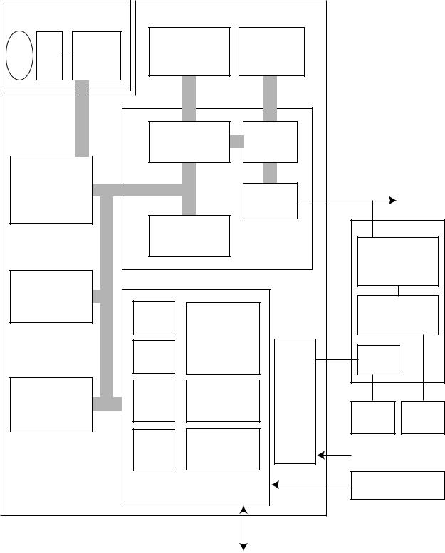
BLOCK DIAGRAM
Camera Unit |
Digital PCB |
|
|
|
|||
|
|
|
IC701 |
|
IC702 |
|
|
|
|
A/D |
|
PD6461GS |
|
|
|
Lens |
CDD |
PD482445LGW |
|
|
|||
converter |
On screen |
|
|
||||
|
|
4M bit VRAM |
|
|
|||
|
|
|
display |
|
|
||
|
|
|
|
|
|
|
|
|
|
|
VRAM |
|
Video |
|
|
|
|
|
controller |
encoder |
|
|
|
IC703 |
|
|
|
|
|
|
|
LC99092-Z98 |
|
|
|
|
|
|
|
8 bit to 16 bit |
|
|
|
D/A |
|
Video out |
|
converter |
|
|
|
|
|||
|
|
|
converter |
|
|||
Color processor |
|
|
|
|
|||
|
|
|
|
|
|||
|
|
|
Data |
|
|
Linear PCB |
|
|
|
|
compressor |
|
IC300 |
|
|
|
|
|
expander |
IC700 |
|
||
|
|
|
IR3P90Y1 (NTSC) |
||||
|
|
|
|
|
HG51D291FE |
||
|
|
|
|
|
IR3Y21 (PAL) |
||
|
|
|
|
|
|
||
IC602 |
|
|
|
|
Chroma circuit |
||
KM29V32000T |
|
|
|
|
|
||
32M bit |
|
|
|
|
IC400 |
|
|
Flash memory |
|
ROM |
Direct |
|
MSM6770CGS |
||
|
|
|
|
Display controller |
|||
|
|
|
|
|
|||
|
|
|
|
memory |
|
|
|
|
|
|
|
access |
|
Power |
|
|
|
|
RAM |
controller |
|
|
|
|
|
|
|
supply |
|
||
|
|
|
|
|
|
|
|
IC601 |
|
|
Bus |
Power |
|
|
|
|
CPU |
state |
|
|
|||
HM51W4260 |
|
supply |
Back |
|
|||
|
|
controller |
|
||||
4M bit DRAM |
|
|
|
LCD |
|||
|
|
|
|
light |
|||
|
|
|
|
|
|
||
|
|
|
|
|
|
|
|
|
|
|
I/O |
Serial |
|
|
|
|
|
|
communication |
AC Adaptor |
|||
|
|
|
port |
||||
|
|
|
interface |
|
Battery |
|
|
|
|
|
|
|
|
||
|
|
|
IC600 |
|
|
Key PCB |
|
|
|
|
HD6437042Y04F |
|
|||
|
|
|
|
|
|
||
Digital I/O
— 2 —

FLOW DIAGRAM
REC mode
1 |
|
|
|
|
|
|
A/D |
2 |
4 |
6 |
8 |
CCD |
IC703 |
|
IC700 |
|
|
Converter |
LC99092-Z98 |
|
HG51D291FE |
||
|
|
||||
Camera Unit |
|
|
|
7 |
|
|
|
|
|
IC701 |
|
|
|
IC602 |
|
µPD482445LGW |
|
|
|
KM29V32000T |
|
|
|
|
|
|
3 |
IC600 |
|
|
|
|
|
|
|
|
|
IC601 |
|
HD6437042Y04F |
|
|
|
5 |
|
|
|
|
|
HM51W4260 |
|
|
|
|
|
|
|
Digital PCB |
|
1 Exposure and Analog to Digital conversion by Camera unit
2 8 to 16 bits conversion by IC703
3 Storage for work
4 Color processing by IC703: Ye,Cy, Gr → Y, By, Ry
5 Storage for work
6, 7 Video encode by IC700 and IC701: Y, By, Ry → Video
8 Video out
When pressing the shutter button |
|
|
||
1 |
|
|
|
|
|
A/D |
2 |
4 |
6 |
CCD |
IC703 |
|
IC700 |
|
Converter |
LC99092-Z98 |
|
HG51D291FE |
|
|
|
|||
Camera Unit |
|
|
|
|
|
|
|
|
IC701 |
|
|
IC602 |
|
µPD482445LGW |
|
|
KM29V32000T |
|
|
|
|
8 |
|
|
|
|
|
3 |
IC600 |
|
|
|
|
|
|
|
IC601 |
5 |
HD6437042Y04F |
|
|
HM51W4260 |
|
|
|
|
7 |
|
Digital PCB |
|
|
— 3 — |
|
|
1 Exposure and Analog to Digital conversion by Camera unit
2 8 to 16 bits conversion by IC703
3 Storage for work
4 Color processing by IC703: Ye, Cy, Gr → Y, By, Ry
5 Storage for work
6 Compression by IC700
7 Storage for work
8 Storage to Flash memory
PLAY mode
|
|
|
|
2 |
|
A/D |
IC703 |
|
6 |
CCD |
|
IC700 |
||
Converter |
LC99092-Z98 |
|
HG51D291FE |
|
|
|
|||
|
|
|
|
4 |
Camera Unit |
|
|
5 |
|
|
|
|
|
|
|
|
|
|
IC701 |
|
|
IC602 |
|
µPD482445LGW |
|
|
KM29V32000T |
|
|
|
|
1 |
|
IC600 |
|
|
|
|
|
|
|
IC601 |
3 |
HD6437042Y04F |
|
|
|
||
|
|
HM51W4260 |
|
|
|
|
|
|
|
|
|
|
|
Digital PCB |
1 Reading from Flash memory and storage for work
2 Expansion by IC700
3 Storage for work
4, 5. Video encode by IC700 and IC701: Y, By, Ry → Video
6 Video out
— 4 —

CN601
KEY0
KEY2
1 PON from  PON Key PCB KEY1
VCC3-1
VCC3-1
GND
GND
POWER SUPPLY CIRCUIT OPERATION |
|
||||||||
|
|
|
|
|
|
|
|
|
2 APO from Pin 42 |
|
|
|
|
|
|
|
|
R517 |
of IC600 |
|
|
|
|
|
|
VCC1 |
|
||
|
|
|
|
|
|
|
|
||
|
|
|
|
|
|
|
R515 |
|
|
|
|
|
|
IC507 |
|
2 |
Q514 |
|
|
FU500 |
R516 |
|
1 OUT NC 5 |
C521 |
|
|
3 |
|
|
+ |
1 |
|
|
|
|||||
|
+ |
3 VDD |
|
|
|
||||
|
|
|
2 |
|
|
|
|
|
|
|
|
|
GND NC 4 |
|
|
|
C523 |
|
|
C548 |
C531 |
|
|
|
|
|
|
|
|
|
VCC1 |
|
VCC1 |
|
|
|
6 Voltage detection signal |
||
|
|
|
|
|
VCC3-1 |
|
|||
|
|
|
|
R623 |
|
|
|
||
|
R510 |
|
3 |
IC506 |
8 7 6 5 |
|
R514 |
3 POB to Pin102 |
|
|
|
|
|
1 2 3 4 |
|
||||
|
|
|
C520 |
1 |
|
VCC PR CLR Q |
|
|
|
|
|
|
|
|
|
CK D Q GND |
|
|
|
|
R511 |
R512 |
Q503 |
|
|
|
2 |
of IC600 |
|
|
2 |
|
|
|
|
|
|||
|
|
|
|
|
|
|
|
|
|
2 |
|
|
C254 |
|
|
|
3 |
|
|
|
|
|
|
|
Q513 1 |
|
|||
1 |
|
|
|
R513 |
|
|
|||
|
|
|
|
|
|
|
|
||
3 |
|
|
|
|
|
|
|
|
|
4 |
|
|
|
|
|
|
|
|
|
5 |
|
|
|
|
|
VCC1 |
|
|
|
6 |
VCC3-1 |
|
VCC1 |
|
|
|
|||
|
|
|
|
|
|
||||
7 |
|
|
|
|
|
|
|||
|
|
|
|
|
|
R509 |
|
||
8 |
|
|
|
IC505 |
|
|
|
||
|
|
|
|
|
|
|
|
||
|
|
|
|
|
|
|
|
|
|
4 OUT GND |
3 |
|
|
5 |
INA |
2 |
2 Q512 |
VCC INB |
1 |
||
|
3 |
|
4 FACT from |
1 |
Pin 36 of IC600 |
|
|
|
|
5 Power ON to Pin 3 of Q505 |
|
|
|
|
|
Signal |
|
Operation |
|
|
|
|
1 |
PON |
Power on/off signal (pulse) from SW900 on Key PCB |
|
|
|
|
|
2 |
APO |
Auto power off signal (pulse) from pin 42 of IC600 |
|
|
|
|
|
3 |
POB |
Power on/off recognition signal to pin 102 of IC600 |
|
|
|
ON: H (VCC3) |
OFF: L (GND) |
|
|
|
|
4 |
FACT |
Forced power on signal from pin 36 of IC600 |
|
|
|
Forced ON: H (VCC3) OFF: L (GND) |
|
|
|
ex. While writing to flash memory |
|
|
|
|
|
5 |
Power On |
Power on/off signal to pin 3 of Q505 |
|
|
|
ON: H (VCC1) |
OFF: L (GND) |
|
|
|
|
6 |
Voltage |
Normal: H |
|
|
detection |
Low voltage: L |
|
|
|
|
|
— 5 —

IC |
|
|
|
|
|
Operation |
||||||
IC505 |
NAND gate |
1 |
|
|
|
4 |
|
|
|
|||
|
|
|
|
|
|
|
|
|
||||
|
|
|
2 |
|
|
|
|
|
|
|
|
|
IC506 |
Flip-flop |
|
|
|
|
|
|
|
|
|
|
|
|
|
1 |
|
|
|
|
|
|
|
8 |
|
|
|
CK |
|
VCC |
|||||||||
|
2 |
7 |
|
|||||||||
|
|
D |
|
|
|
|
|
|
||||
|
|
|
|
PR |
|
|||||||
|
|
3 |
|
|
6 |
|
||||||
|
|
|
|
|
|
|
|
|
||||
|
|
Q |
|
CLR |
|
|
||||||
|
|
|
||||||||||
|
|
4 |
5 |
|
||||||||
|
|
GND |
|
Q |
|
|||||||
|
|
|
||||||||||
IC507 |
Voltage detector |
|
|
|||||||||
|
|
|
|
|
|
|
|
|
|
|||
|
|
|
|
|
|
|
|
|
|
|||
|
|
Pin 2 (VDD) |
Pin 1 (OUT) |
|||||||||
|
|
|
|
|
|
|
|
|
|
|||
|
|
|
|
> 3.2 V |
|
|
|
|
H |
|||
|
|
|
|
|
|
|
|
|
|
|||
|
|
|
|
< 3.2 V |
|
|
|
|
L |
|||
|
|
|
|
|
|
|
|
|
|
|
|
|
|
|
|
|
|
|
|
|
|
|
|
|
|
Time Chart
Power on |
|
Power off |
|
1. PON |
H (VCC1) |
1. PON |
|
L |
|||
|
|
||
2. APO |
L |
2. APO |
|
|
|
||
3. POB |
H (VCC3) |
3. POB |
|
L |
|||
|
|
||
4. FACT |
L |
4. FACT |
|
|
|
||
5. Power On |
H (VCC1) |
5. Power On |
|
L |
|||
|
|
||
6. Voltage |
H (VCC0) |
6. Voltage |
|
|
|||
detection |
|
detection |
H (VCC1) L
L
H (VCC3) L
L
H (VCC1) L
H (VCC0) L
— 6 —
Power off by APO
1.PON
2.APO
3.POB
4.FACT
5.Power On
6.Voltage detection
Forced power on by FACT
1.PON
2.APO
3.POB
4.FACT
5.Power On
6.Voltage detection
H (VCC1)
H (VCC3) L
H (VCC3) L
L
H (VCC1) L
H (VCC0)
H (VCC1)
L
L
H (VCC3) L
H (VCC1) L
H (VCC0)
Power off by low voltage detection
1.PON
2.APO
3.POB
4.FACT
5.Power On
6.Voltage detection
H (VCC1)
L
H (VCC3) L
L
H (VCC1) L
H (VCC0) L
— 7 —

MEMORY RESET AND COLOR ADJUSTMENT
When the repairing or the following problems occured on QV-200, make the memory reset and the color adjustment as shown below.
A)After replacement of Digital PCB or Camera unit
B)Memory error
C)No display caused by Memory error
D)Color tone problem
MEMORY ERROR
"Memory error" (#1 ~ #4) message appears on QV-200 camera, when an error is found in its flash memory. In this case, the QV-200 is locked up and do not accept any operation except power on/off.
!
MEMORY ERROR
#1
CONSULT
THE OWNERíS MANUAL
It is required to reset the flash memory and adjust the color information.
NO DISPLAY CAUSED BY MEMORY ERROR
When the memory error occures, sometimes the display and back light do not work.
In this case, it is required the flash memory reset and color adjustment, same as the case of memory error.
COLOR TONE PROBLEM
In this case, do the color adjustment only.
REQUIRED TOOL
Light box: Handy 5000 (Code No.: 1904 5301) It used for QV-100 also.
Batteries for the light box: 4 × LR20 (D) size alkaline batteries
Color temperature filter (Code No.: 1904 5363): LA-120 (Orange)
ND filter (Code No.: 1904 5362): ND-50 (Grey)
Adjustment software: SDJ775A.EXE
QV-Link software: LK-10V (For VGA)
TO SOLVE THE PROBLEMS
MEMORY ERROR
1.Save the image (CAM files) of the QV-200 to PC by using QV-Link software.
*Although the memory error #1 and #2 occures, sometimes the image can be transfered to PC. The image transfer is impossible in the memory error #3 and #4.
2.Execute the memory reset and color adjustment by SDJ775A.EXE.
3.Reload the image to QV-200 by using QV-Link.
—8 —
 Loading...