

Page 1
(without price)
CTK-2000
INDEX
MAY. 2008
CTK-2000
ELECTRONIC KEYBOARD
Ver.2 : Nov. 2008
Page 2

CONTENTS
SPECIFICATIONS ------------------------------------------------------------------------------------------ 1
BLOCK AND WIRING DIAGRAM --------------------------------------------------------------------- 2
PCB LAYOUT ----------------------------------------------------------------------------------------------- 3
CIRCUIT DESCRIPTION --------------------------------------------------------------------------------- 4
PRINTED CIRCUIT BOARDS -------------------------------------------------------------------------- 5
DISASSEMBLY --------------------------------------------------------------------------------------------- 8
DIAGNOSTIC PROGRAM ------------------------------------------------------------------------------13
EXPLODED VIEW ----------------------------------------------------------------------------------------16
PARTS LIST ------------------------------------------------------------------------------------------------17
SCHEMATIC DIAGRAMS -------------------------------------------------------------------------------20
Page 3

SPECIFICATIONS
Keyboard
Maximum Polyphony
Tones
Built-in Tones
Sampling Tones
Reverb
Metronome
Beats per Measure
Tempo Range
Song Bank
Tunes
Step Up Lesson
Lessons
Lesson Part
Functions
Music Challenge
Auto Accompaniment
Rhythm Patterns
Other Functions
Transpose
Tuning
MIDI
Musical Information Function
Inputs/Outputs
USB port
Sustain jack
Phones/Output jack
Audio In jack
Power Jack
Power Supply
Batteries
Battery Life
AC Adaptor
Auto Power Off
Speakers
Output
Power Consumption
Dimensions
Weight
61 standard-size keys
48 notes (24 for certain tones)
400
1
Sampling time: 1 second (fixed)
Effects: 10 types
1 to 10, Off
0, 2 to 6
30 to 255
110
4 (Listen, Watch, Remember, Auto)
L, R, LR
Repeat, Voice Fingering Guide, Note Guide, Performance Evaluation
20 notes
150
±1 octaves (12 semitones)
A4 = approx. 440 Hz ±100 cents
16 multi-timbre received, GM Level 1 standard
Tone, Rhythm, Song Bank, numbers and names; staff notation, fingering,
pedal operation, tempo, measure and beat number, chord name, etc.
TYPE B
Standard jack (sustain, sostenuto, soft, rhythm start/stop)
Stereo standard jack
Output Impedance: 200Ω, Output Voltage: 4.8V (RMS) MAX
Stereo mini jack
Input Impedance: 40kΩ, Input Sensitivity: 200mV
9V DC
2-way
6 AA-size zinc-carbon batteries or alkaline batteries
Approximately 4 hours continuous operation on alkaline batteries
AD-5
Approximately 6 minutes after last key operation (Operates during battery use only)
10cm × 2
2W + 2W
9V 7.7W
94.9 × 35.4 × 11.2 cm (37 3/8× 13 15/16× 4 7/16inch)
Approximately 3.8kg (8.4 lbs) (without batteries)
– 1 –
Page 4
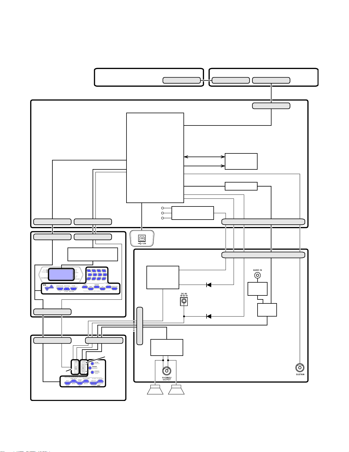
BLOCK AND WIRING DIAGRAM
MAIN PCB
(M800-MDA1)
SUB PCB
(M800-PSA1)
CONSOLE PCB
(M800-CNA)
CONSOLE PCB (M800-CNB)
MA1 ~ MA21
DB4 ~ DB7,E,R/W,RS (LCD signal)
KC0 ~ KC7,KI1,KI2,F19,FI10 (Button signal)
NMI
VE5
VD5
VD3
NMI
VCP
VCP
D103
MD0 ~ MD15
KC0 ~ KC7,FI0 ~ FI3,SI0 ~ SI3
P2ROM
(16Mbit)
IC2
POWER
CIRCUIT
Q101,Q102,
D104,D106
Power
Amplifier
IC101
LCD CONTROLLER
IC401
D/D CONVERTER
IC4,IC5
M800-KYA2 M800-KYA1
LOUT,ROUT
APO
APO
VC
VC
ADIN
PEDAL
(L) (R)
Filter
IC3
Filter
IC2
Filter IC6
D107
MPU
IC1
CN801 (13pin)
CN1 (16pin)
CN6 (10pin)CN5 (12pin) CN3 (11pin)
CN109 (11pin)
CN404 (10pin)CN405 (12pin)
CN401 (8pin)
CN302 (8pin) CN301 (8pin)
CN106 (8pin)
CN803 (16pin)CN802 (13pin)
PHONES
POWER SW
MIAN VOL
SPEAKERS
LCD
USB
DC JACK
AUDIO IN
PEDAL
– 2 –
Page 5
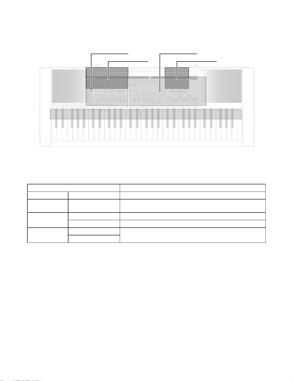
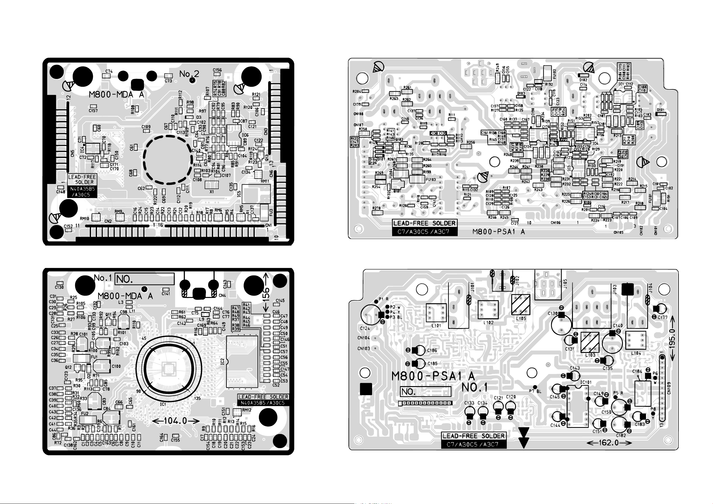
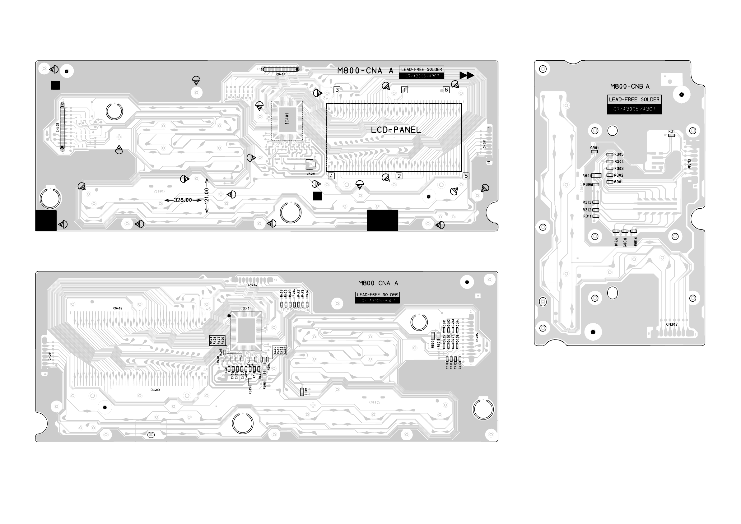
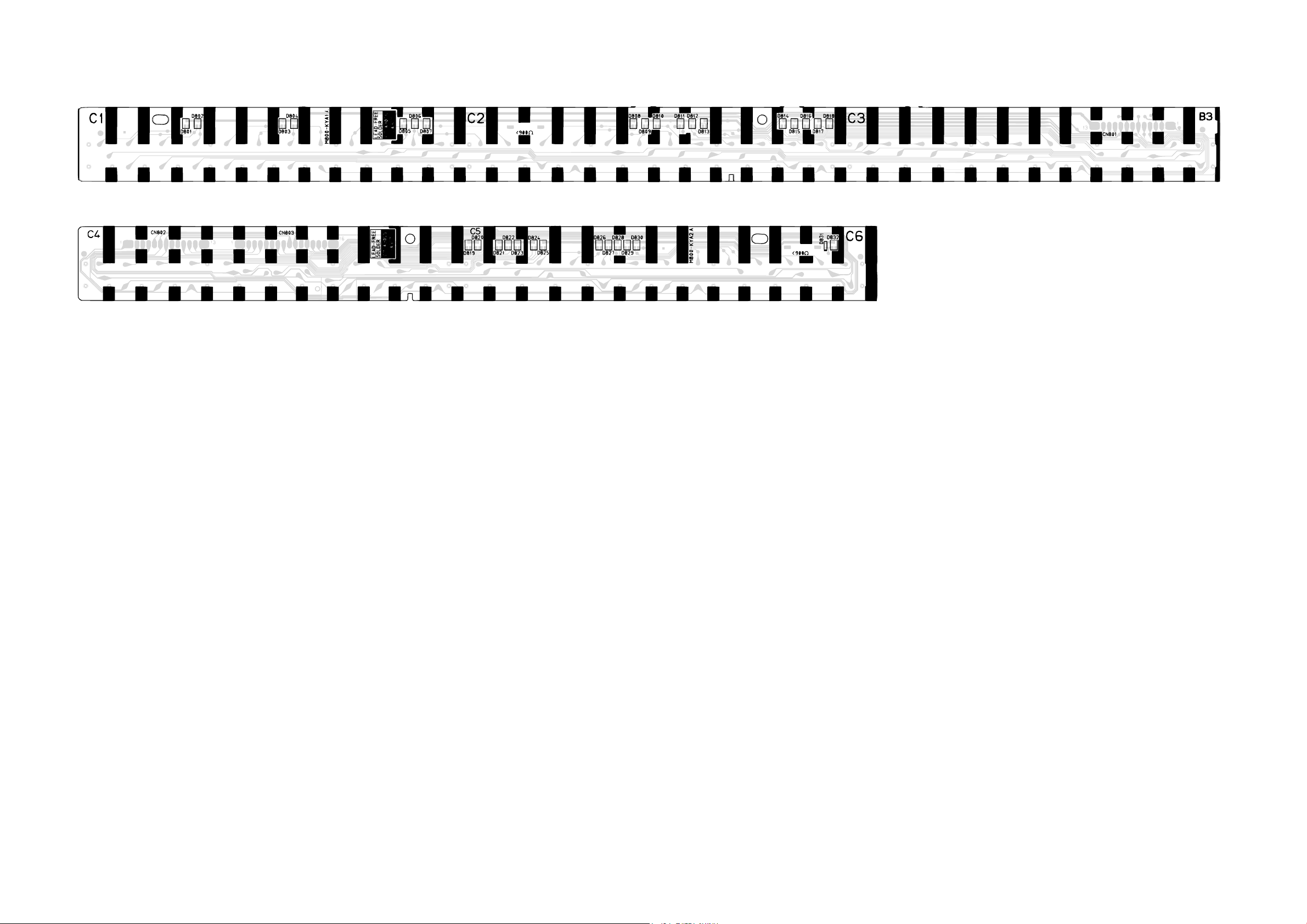
PCB LAYOUT
M800-MDA1 PCB
M800-CNA PCB
M800-PSA1 PCB
M800-CNB PCB
M800-KYA1 PCB M800-KYA2 PCB
PCB Components
MAIN PCB M802-MDA1 MPU, ROM(16Mbit), D/D converter, USB terminal
SUB PCB M800-PSA1 Power supply circuit, Power amplifer
Phones terminal, Pedal terminal, Audio terminal, DC JACK
Console PCBs M802-CNA LCD controller, Button
M802-CNB Power switch, Main volume, Button
Keyboard PCBs M802-KYA1 Keyboard
M802-KYA2
– 3 –
Page 6
CIRCUIT DESCRIPTION
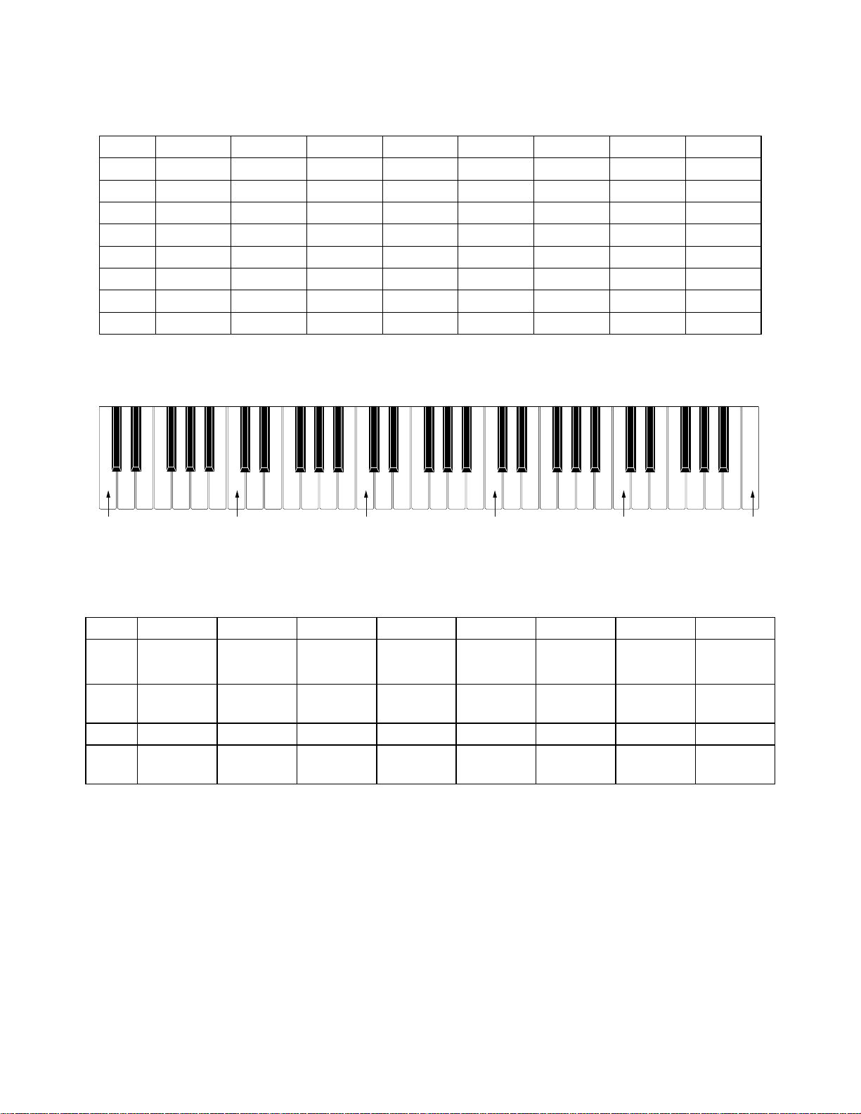
C2 C3 C4 C5 C6 C7
KEY MATRIX
KC0 KC1 KC2 KC3 KC4 KC5 KC6 KC7
KI0 C2 C2# D2 D2# E2 F2 F2# G2
KI1 G2# A2 A2# B2 C3 C3# D3 D3#
KI2 E3 F3 F3# G3 G3# A3 A3# B3
KI3 C4 C4# D4 D4# E4 F4 F4# G4
KI4 G4# A4 A4# B4 C5 C5# D5 D5#
KI5 E5 F5 F5# G5 G5# A5 A5# B5
KI6 C6 C6# D6 D6# E6 F6 F6# G6
KI7 G6# A6 A6# B6 C7
NOMENCLATURE OF KEYS
BUTTON MATRIX
KC0 KC1 KC2 KC3 KC4 KC5 KC6 KC7
KI1 TONE SONG
KI2 RHYTHM
KI9 0 1 2 3 4 5 6 -
KI10 7 8 9 + GUIDE PAUSE
TEMPO
DOWN
TEMPO
UP
TYPE
GAME
PHRASE
WAIT
START/
STOP
PLAY/
STOP
REW FUNCTION FF
METRONOME REPEAT
PART
SELECT
SAMPLING
– 4 –
Page 7
– 5 –
PRINTED CIRCUIT BOARDS
Main PCB M800-MDA1
Sub PCB M800-PSA1
Top View
Bottom View
Top View
Bottom View
Page 8
– 6 –
Console PCB M800-CNB
Top View
Bottom View
Console PCB M800-CNA
Page 9
– 7 –
Key PCB M800-KYA1
Key PCB M800-KYA2
Page 10

DISASSEMBLY
1. Remove the battery cover and then battery.
2. Remove 11 screws and then upper case.
3. Remove two lead wires by soldering.
4. Remove cable by soldering.
5. Make the keyboard unit and the main unit apart.
Cable (CN1)
– 8 –
Read wire (Red)
Read wire (Black)
Page 11

6. To remove the main PCB (M800-MDA1).
6-1. Remove three screws on the PCB (M800-MDA1).
6-2. Remove three cables by soldering.
6-3. Remove the PCB (M800-MDA1).
Cable (CN5)
Cable (CN6)
7. To remove the sub PCB (M800-PSA1).
7-1. Remove four screws on the PCB (M800 7-2. Remove one cable by soldering.
7-3. Remove four lead wires by soldering.
7-4. Remove the PCB (M800-
PSA1
).
PSA1
).
Cable (CN3)
Precaution while assembling the main Connector 3.
Number of pins on the PCB and pins on the cable
are different.
Start connecting from the NO.1 pin whose color is
orange.
Read wire (Brown)
Read wire (Green)
Read wire (Blue)
Read wire (White)
Cable (CN106)
Precaution while assembling the main Connector 106.
Number of pins on the PCB and pins on the cable are different.
Start connecting from the NO.1 pin whose color is orange.
– 9 –
Page 12

8. To remove the console PCBs (M800-CNA, M800-CNB).
8-1.
Remove the volume and Power knob.
8-2. Remove 29 screws and then the PCBs (M800-CNA and M800-CNB).
Caution while assembling:
6 s c re w s fi x at i ng t h e L CD un i t mu s t b e
3 1 6
screwe d on in ades i gn a t ed ord e r.W he n
assembling, be sure to tighten the screws in
theorder from 1 - 6 shown in the photo.Failing
to do so may cause display malfunctions.
4 2 5
9. Remove the rubber keys.
10. Remove 8 screws and then two speakers.
– 10 –
Page 13

11. To remove the key PCBs (M800-KYA1/KYA2)
11-1. Remove eight screws and then two side cases.
11-2. Remove 21 screws and then the white keys.
– 11 –
Page 14

11-3. Remove the black keys.
11-4. Remove the hooks and then Key PCB. (M800-KYA1/KYA2)
11-5. Remove the rubber keys.
4 25 3 1
Caution while assembling:
There are two types of rubber keys and they are different in length.
The longest rubber key ( ) must be installed at the right end.
1
How to install the rubber keys.
– 12 –
Page 15

DIAGNOSTIC PROGRAM
1:SW
1:SW
001
F
1:SW OK!
1F
1E
1D
1C
03
04
05
06
07
0E
09
08
0D
0A
0B
SW OK!
10 11 12
161B 14 15
191A 17 18
02 01 00
0F
0C
TESTMODE
TEST
1-9
Initial Setting
1. Connect the AC adaptor.
2. "Main" volume: MAX
How to start diagnostic program
1. Press and hold the "0", "1" and "2" buttons.
2. Press the "POWER" button.
3. The massage "TESTMODE" is appears on LCD.
4. Release the "0", "1" and "2" buttons.
Diagnostic program
Message on LCD
1. Button check
Press "1" button.
Press the button in the order indicated in the illustration below.
The button number will be displayed on the LCD.
Example) SW00 + (the button number shown in the illustration)
Press "SETTING" button.
If the switch function is OK: You will hear the OK sound signal and the button number will be displayed.
If the switch function is NG or switches were pressed in a wrong order: You will hear the NG sound signal
and the button number will be displayed.
Press the "3" button the last.
Press "0" to end the LCD Check.
– 13 –
Page 16

1:AD1
XXX
000 to 3FF
1:AD3
XXX
000 to 1FF
TEST
1-9
5267
Message on LCD
MX
800
TEST
1-9
2:LCD
TEST
1-9
2. AC adaptor check
Press "3" button.
* Make sure that a value "XXX" shown in the illustration is in the
range of 000 to 3FF.
Press "3" button.
* Make sure that a value "XXX" shown in the illustration is in the
range of 000 to 1FF.
Press "0" to end the AC adaptor Check.
3. ROM Version and Model check
Press "9" button. (ROM Version)
* "5267" must be displayed.
Press "9" button. (Model)
* "MX800" must be displayed.
Press "0" to end the ROM Version and Model Check.
4. LCD check
Press "2" button.
Press "2" button.
* All dots and characters of LCD turn on.
* There is no lack of the dot and the charater.
Press "2" button.
* LCD no display.
Press "0" to end the LCD Check.
– 14 –
Page 17

5. USB check
* Operating System
Windows® XP (SP2 or later)*1
Windows Vista® *2
Mac OS® X (10.3.9, 10.4.11 or later, 10.5.2 or later)
*1: Windows XP Home Edition
Windows XP Professional (32- bit)
*2: Windows Vista (32- bit)
Connect CTK-2000 to the computer with a USB cable.
Check that the message "USB AUDIO DEVICE" appears in "Device Manager" → "Sound, Video and
Game Controller" on the computer monitor.
Disconnect the USB cable.
Check that the message "USB AUDIO DEVICE" disappears in "Device Manager" → "Sound, Video and
Game Controller" on the computer monitor.
DIAGNOSTIC PROGRAM IS FINSHED.
– 15 –
Page 18

EXPLODED VIEW
6
7
4
5
10
8
11
9
16
12
15
14
20
21
1
22
19
18
17
13
23
23
R-1
R-3
R-2
3
2
24
25
R-5
R-6
R-7
R-4
– 16 –
Page 19

PARTS LIST
CTK-2000
Notes: This parts list does not include the cosmetic parts,
which parts are marked with item No. “R-X” in the
exploded view.
Contact our spare parts department if you need
these parts for refurbish.
1. Prices and specifications are subject to change
without prior notice.
2. As for spare parts order and supply, refer to
the “GUIDEBOOK for Spare parts Supply”,
published seperately.
3. The numbers in item column correspond to the
same numbers in drawing.
– 17 –
Page 20

1 CTK-2000_DI
1 2 3 4 5
Main PCB
N 1 10304685
PCB ASSY/MDA1 TK-RJM508605*001
1 1 1 1 1 CU A
D3 10276977 CHIP DIODE L1SS400T1G 1 1 1 1 1 AA X
D2 79114195 DIODE UDZSTE-175.6B 1 1 1 1 1 AA X
IC6 10211950 I.C NJM2068M-D(TE1) 1 1 1 1 1 AC C
IC4 10269340 IC XC6403FY51PR 1 1 1 1 1 AE X
L9 10193074 COIL DLW21HN181SQ2L 1 1 1 1 1 AC X
L11 10238668 CHIP BEAD CORE EBMS160808A102 1 1 1 1 1 AA X
Sub PCB
N 2 10304686
PCB ASSY/PSA1 TK-RJM508607*001
1 1 1 1 1 CM B
J104 10206815 CONNECTOR JY-6314*01-030 1 1 1 1 1 AA C PEDAL JACK
L103,105 10231919 COIL RB53-856396NP 2 2 2 2 2 AA X
L102,104 10231920 COIL RB53-856397NP 2 2 2 2 2 AA X
J102 10088189 DC JACK DS-240A2-383V4H 1 1 1 1 1 AC C
D103,104,106,107 10276977 CHIP DIODE L1SS400T1G 4 4 4 4 4 AA X
D101,102 10210387 DIODE RSX101VA-30TR 2 2 2 2 2 AA X
IC2,IC3,IC4 10211950 I.C NJM2068M-D(TE1) 3 3 3 3 3 AC X
Q101 22592702 CHIP TRANSISTOR 2SB1188T100R 1 1 1 1 1 AB X
Q102 69300298 CHIP TRANSISTOR 2SC4081T106R 1 1 1 1 1 AA X
Console PCBs
N 3 10304684
PCB ASSY/CNA1 TK-RJM508599*001
1 1 1 1 1 CO C
IC401 10222381 LSI ST7066U-0A-QG 1 1 1 1 1 AU C
TH401 10138692 THERMISTOR NCP18XH103J03RB 1 1 1 1 1 AA X
VR401 69304870 VOLUME EVND8AA03B53 1 1 1 1 1 AA X
D401-408 10276977 CHIP DIODE L1SS400T1G 8 8 8 8 8 AA X
Keyboard PCB
s
N 4 10304689
PCB UNIT/RUBBER TK-RJM508597*001
1 1 1 1 1 CB C
N 5 10304690
PCB ASSY/KYA K-RJM508609*001
1 1 1 1 1 CB C
Keyboard Uni
t
6 10163902
RUBBER/CONTACT/CB RJM503854-001
4 4 4 4 4 AD B
7 10163903
RUBBER/CONTACT/CS RJM503855-001
1 1 1 1 1 AG B
N 8 10304687
WHITE KEY/CB TK-RJM507243*002
4 4 4 4 4 AW C
N 9 10304688
WHITE KEY/CS TK-RJM507244*002
1 1 1 1 1 AX C
10 10274032 BLACK KEY/10P RJM506595-001V02 2 2 2 2 2 AL C
11 10274160 BLACK KEY/5P RJM506595-002V02 1 1 1 1 1 AE C
Case Uni
t
N 12 10301466 PLATE/DISPLAY RJM508541-001V01 1 1 1 1 1 AG C
13 10199714 KNOB/SLIDE RJM503803-002V01 2 2 2 2 2 AB C
14 69095890 CONTACT/SLIDE CSB-12D 2 2 2 2 2 AC C
N 15 10301465 CONNECTOR RJM508539-001V01 2 2 2 2 2 AD C
N 16 10301473 LCD TY-11151N 1 1 1 1 1 AZ C
N 17 10301453 RUBBER KEY/A RJM508524-001V01 1 1 1 1 1 AH C
N 18 10301454 RUBBER KEY/B RJM508525-001V01 1 1 1 1 1 AJ C
N 19 10301455 RUBBER KEY/C RJM508526-001V01 1 1 1 1 1 AH C
N 20 10301456 RUBBER KEY/D RJM508527-001V01 1 1 1 1 1 AH C
N 21 10301457 RUBBER KEY/E RJM508528-001V01 1 1 1 1 1 AL C
N 22 10301458 RUBBER KEY/F RJM508529-001V01 1 1 1 1 1 AJ C
23 10264808 SPEAKER C10J01A 2 2 2 2 2 AJ C
24 10243428
COVER ASSY/BATTERY TK-M340884*020
1 1 1 1 1 BE C
25 10310585 PCB ASSY/PSA2 TK-RJM509016*001 1 1 1 1 1 BV C
QTY
Price
Code
N Item Parts No. Parts Name Specification R Remarks
2 CTK-2000_CHINA
3 CTK-2000_EU
4 CTK-2000_UK
5 CTK-2000_US
– 18 –
Page 21

1 CTK-2000_DI
1 2 3 4 5
Accessorie
s
- 10118186 STAND/MUSIC M311760-001V02 1 1 1 1 1 AK C
Refurbish
N R-1 10301447 PANEL RJM508496-001V01 1 1 1 1 1 CP C
N R-2 10301445 PANEL/SIDE/L RJM508445-001V01 1 1 1 1 1 AQ C
N R-3 10301446 PANEL/SIDE/R RJM508446-001V01 1 1 1 1 1 AQ C
N R-4 10313606 CASE UNIT/MAIN
TK-RJM508586*001
1 1 1 1 1 DC C
N R-5 10302799 LOWER COVER/A RJM508655-001V01 1 1 1 1 1 AD X
N R-6 10302800 LOWER COVER/B RJM508656-001V01 1 1 1 1 1 AD X
N R-7 10302801 LOWER COVER/C RJM508657-001V01 1 1 1 1 1 AD X
N Item Parts No. Parts Name RemarksSpecification
QTY
Price
Code
R
2 CTK-2000_CHINA
3 CTK-2000_EU
4 CTK-2000_UK
5 CTK-2000_US
– 19 –
Page 22

– 20 –
Not used: C28,L3
Not used
Not used:
pin12,pin13
Not used:
C170
Not used
SCHEMATIC DIAGRAMS
Main PCB M800-MDA1
Page 23

– 21 –
Not used
Not used: pin9,pin10
Not used
Not used
Not used
Not used:
FU104
Not used: R153
Not used:
pin12,pin13
Sub PCB M800-PSA1
Page 24

– 22 –
Console PCB M800-CNA
Page 25

– 23 –
Console PCB M800-CNB
Page 26

– 24 –
Keyboard PCBs M800-KYA1/KYA2
Page 27

Ver.1 : Oct. 2008
• Addition of The DISASSEMBLY (P8 to P11)
• Addition of The DIAGNOSTIC PROGRAM (P14)
Ver.2 : Nov. 2008
• Correction of The BLOCK AND WIRING DIAGRAM (P2)
• Correction of The PCB LAYOUT (P3)
CASIO COMPUTER CO.,LTD.
Overseas Service Division
6-2, Hon-machi 1-Chome
Shibuya-ku, Tokyo 151-8543, Japan
 Loading...