


BSI BS62LV256PC, BS62LV256JI, BS62LV256JC, BS62LV256DI, BS62LV256DC Datasheet
...
|
BSI |
Very Low Power/Voltage CMOS SRAM |
|
||
|
32K X 8 bit |
|
|
BS62LV256 |
|
FEATURES |
|
DESCRIPTION |
|
||
• Wide Vcc operation voltage : 2.4V ~ 5.5V |
The BS62LV256 is a high performance, very low power CMOS |
||||
• Very low power consumption : |
Static Random Access Memory organized |
as 32,768 words by 8 bits |
|||
Vcc = 3.0V C-grade : 20mA (Max.) operating current |
and operates from a wide range of 2.4V |
to 5.5V supply voltage. |
|||
|
I- grade : 25mA (Max.) operating current |
Advanced CMOS |
technology and circuit techniques provide both high |
||
|
0.01uA (Typ.) CMOS standby current |
speed and low power features with a typical CMOS standby current of |
|||
Vcc = 5.0V C-grade : 35mA (Max.) operating current |
0.01uA and maximum access time of 70ns in 3V operation. |
||||
|
I- grade : 40mA (Max.) operating current |
Easy memory expansion is provided by active LOW chip |
|||
|
0.4uA (Typ.) CMOS standby current |
enable (CE), active LOW output enable (OE) and three-state |
|||
• High speed access time : |
|
output drivers. |
|
|
|
-70 |
70ns (Max.) at Vcc=3.0V |
The BS62LV256 |
has an automatic power down feature, reducing the |
||
• Automatic power down when chip is deselected |
power consumption significantly when chip is deselected. |
||||
The BS62LV256 |
is available in the DICE form, JEDEC standard |
||||
• Three state outputs and TTL compatible |
28pin 330mil Plastic SOP, 300mil Plastic SOJ, 600mil Plastic DIP and |
||||
• Fully static operation |
|
8mmx13.4mm TSOP (normal type). |
|
||
•Data retention supply voltage as low as 1.5V
•Easy expansion with CE and OE options
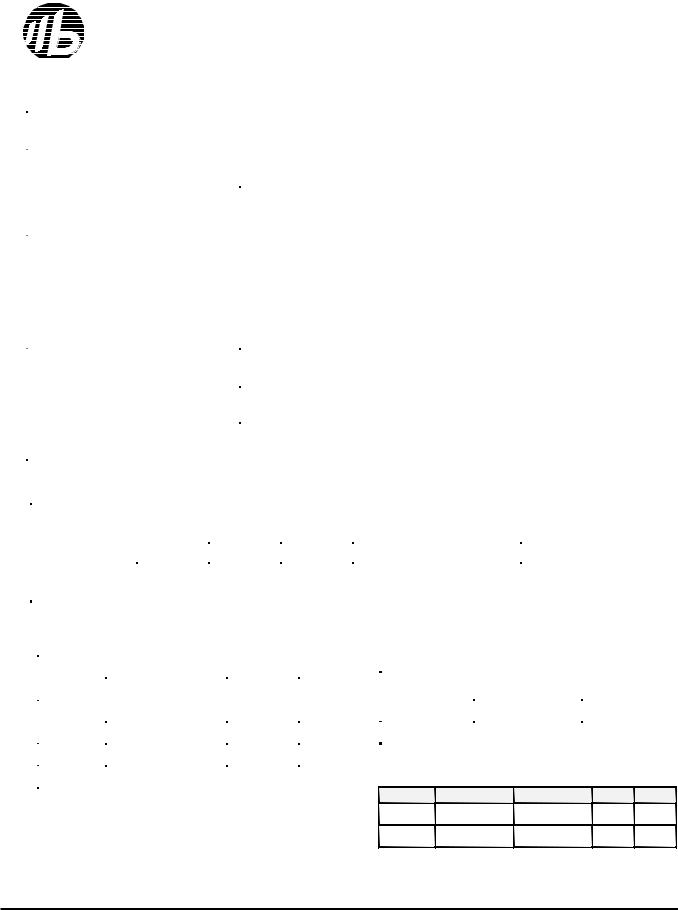
PRODUCT FAMILY
|
|
|
SPEED |
|
POWER DISSIPATION |
|
|
||
PRODUCT |
OPERATING |
Vcc |
STANDBY |
Operating |
PKG |
||||
(ns) |
|||||||||
FAMILY |
TEMPERATURE |
RANGE |
Vcc= |
(ICCSB1, Max) |
(ICC, Max) |
TYPE |
|||
|
|
|
Vcc= |
Vcc= |
Vcc= |
Vcc= |
|
||
|
|
|
3.0V |
5.0V |
3.0V |
5.0V |
3.0V |
|
|
|
BS62LV256SC |
|
|
|
|
|
|
|
|
SOP-28 |
|
BS62LV256TC |
0 O C to +70 O C |
2.4V ~ 5.5V |
|
70 |
1uA |
0.2uA |
35mA |
20mA |
TSOP-28 |
|
BS62LV256PC |
|
PDIP-28 |
|||||||
|
BS62LV256JC |
|
|
|
|
|
|
|
|
SOJ-28 |
|
BS62LV256DC |
|
|
|
|
|
|
|
|
DICE |
|
BS62LV256SI |
|
|
|
|
|
|
|
|
SOP-28 |
|
BS62LV256TI |
-40 O C to +85 O C |
2.4V ~ 5.5V |
|
70 |
2uA |
0.4uA |
40mA |
25mA |
TSOP-28 |
|
BS62LV256PI |
|
PDIP-28 |
|||||||
|
BS62LV256JI |
|
|
|
|
|
|
|
|
SOJ-28 |
|
BS62LV256DI |
|
|
|
|
|
|
|
|
DICE |
PIN CONFIGURATIONS |
|
|
BLOCK DIAGRAM |
|
|
|
||||
|
|
A14 |
|
1• |
28 |
|
|
VCC |
|
|
|||
|
|
|
|
|
|
|
|||||||
|
|
|
|
|
|
|
|||||||
|
|
A12 |
|
2 |
|
27 |
|
|
WE |
|
|
|
|
|
|
|
|
|
|
|
|
|
|||||
|
|
A7 |
|
3 |
|
26 |
|
|
A13 |
|
|
||
|
|
|
|
|
|
|
|
||||||
|
|
A6 |
|
4 |
|
25 |
|
|
A8 |
|
|
||
|
|
|
|
|
|
|
|
||||||
|
|
A5 |
|
5 |
BS62LV256SC24 |
|
|
A9 |
|
|
|||
|
|
|
|
|
|
|
|||||||
|
|
|
|
|
|
|
|||||||
|
|
A4 |
|
6 |
BS62LV256SI |
23 |
|
|
A11 |
|
|
||
|
|
|
|
|
|
|
|||||||
|
|
A3 |
|
7 |
BS62LV256PC22 |
|
|
OE |
|
|
|
|
|
|
|
A2 |
|
8 |
BS62LV256PI |
21 |
|
|
A10 |
|
|
||
|
|
|
|
|
|
|
|||||||
|
|
|
BS62LV256JC |
|
|
|
|
||||||
|
|
A1 |
|
9 |
20 |
|
|
CE |
|
|
|
||
|
|
|
BS62LV256JI |
|
|
|
|
||||||
|
|
|
|
|
|
|
|||||||
|
|
A0 |
|
10 |
|
19 |
|
|
DQ7 |
|
|
||
|
|
|
|
|
|
|
|
||||||
|
|
|
|
|
|
|
|
||||||
|
|
DQ0 |
|
11 |
|
18 |
|
|
DQ6 |
|
|
||
|
|
|
|
|
|
|
|
||||||
|
|
|
|
|
|
|
|
||||||
|
|
DQ1 |
|
12 |
|
17 |
|
|
DQ5 |
|
|
||
|
|
|
|
|
|
|
|
||||||
|
|
|
|
|
|
|
|
||||||
|
|
DQ2 |
|
13 |
|
16 |
|
|
DQ4 |
|
|
||
|
|
|
|
|
|
|
|
||||||
|
|
|
|
|
|
|
|
||||||
OE |
|
GND |
|
14 |
|
15 |
|
|
DQ3 |
|
A10 |
||
|
|
|
|
|
|
||||||||
|
|
|
|
|
|
||||||||
|
|
|
|
|
|
|
|
|
|
|
|
||
|
|
|
|
|
|
|
|
|
|
|
|
||
|
1• |
|
|
|
28 |
|
|||||||
|
|
|
|
|
|||||||||
A11 |
|
2 |
|
|
|
|
27 |
|
CE |
||||
A9 |
|
3 |
|
|
|
|
26 |
|
DQ7 |
||||
A8 |
|
4 |
|
|
|
|
25 |
|
DQ6 |
||||
A13 |
|
5 |
|
|
|
|
24 |
|
DQ5 |
||||
WE |
|
6 |
|
|
|
|
23 |
|
DQ4 |
||||
VCC |
|
7 |
|
BS62LV256TC |
|
22 |
|
DQ3 |
|||||
A14 |
|
8 |
|
BS62LV256TI |
|
21 |
|
GND |
|||||
A12 |
|
9 |
|
|
|
|
20 |
|
DQ2 |
||||
A7 |
|
10 |
|
|
|
|
19 |
|
DQ1 |
||||
A6 |
|
11 |
|
|
|
|
18 |
|
DQ0 |
||||
A5 |
|
12 |
|
|
|
|
17 |
|
A0 |
||||
A4 |
|
13 |
|
|
|
|
16 |
|
A1 |
||||
A3 |
|
14 |
|
|
|
|
15 |
|
A2 |
||||
A5 |
|
|
|
|
|
|
|
|
|
|
A6 |
|
|
|
|
|
|
|
|
|
|
A7 |
Address |
|
|
|
|
Memory Array |
|
|||
A12 |
18 |
|
512 |
|
|
|||||
|
Row |
|
|
|||||||
A14 |
Input |
|
|
|
|
|
|
|
|
|
|
|
|
|
|
|
|
|
|
||
A13 |
Buffer |
|
Decoder |
|
|
|
512 x 512 |
|
||
A8 |
|
|
|
|
|
|
|
|
||
|
|
|
|
|
|
|
|
|
||
|
|
|
|
|
|
|
|
|
|
|
A9 |
|
|
|
|
|
|
|
|
|
|
A11 |
|
|
|
|
|
|
|
|
|
|
|
|
|
|
|
|
|
|
|
512 |
|
DQ0 |
8 |
|
Data |
8 |
|
|
Column I/O |
|
||
DQ1 |
|
|
Input |
|
|
|
||||
|
|
|
|
|
|
|
|
|
||
DQ2 |
|
|
Buffer |
|
|
Write Driver |
|
|||
|
|
|
|
|
|
|||||
DQ3 |
|
|
|
8 |
|
Sense Amp |
|
|||
DQ4 |
8 |
|
Data |
|
|
|
|
|
|
|
|
|
|
|
|
|
|
|
|||
DQ5 |
|
|
|
|
|
|
64 |
|
||
|
|
Output |
|
|
|
|
|
|
||
DQ6 |
|
|
Buffer |
|
|
|
|
|
|
|
DQ7 |
|
|
|
|
|
Column Decoder |
|
|||
CE |
|
|
|
|
|
|
|
|
12 |
|
Control |
|
|
|
|
|
|
|
|
|
|
WE |
|
|
|
Address Input Buffer |
||||||
OE |
|
|
|
|
|
|
|
|
|
|
Vdd |
|
|
|
|
|
|
|
|
|
|
Gnd |
|
|
|
|
A4 |
A3 |
A2 |
A1 |
A0 |
A10 |
Brilliance Semiconductor Inc. reserves the right to modify document contents without notice.
R0201-BS62LV256 |
1 |
Revision 2.2 |
|
April 2001 |
|
|
|
|
|
|
BSI |
|
|
|
|
|
|
|
|
BS62LV256 |
|||
|
PIN DESCRIPTIONS |
|
|
|
|
|
|
|
|
|
|
|
|
|||||
|
|
|
|
|
|
|
|
|
|
|
|
|
|
|
|
|
|
|
|
|
|
|
|
|
Name |
|
|
|
|
|
|
Function |
|
||||
|
|
|
|
|
|
|
|
|
|
|
|
|
|
|
|
|
|
|
|
|
A0-A14 Address Input |
|
These 15 address inputs select one of the 32768 x 8-bit words in the RAM |
|
|||||||||||||
|
|
|
|
|
|
|
|
|
|
|
|
|
|
|
|
|
|
|
|
|
|
|
|
|
Chip Enable Input |
|
|
is active LOW. Chip enables must be active when data read from or write to the |
|
||||||||
|
|
|
CE |
|
CE |
|
||||||||||||
|
|
|
|
|
|
|
|
device. If chip enable is not active, the device is deselected and is in a standby power |
|
|||||||||
|
|
|
|
|
|
|
|
mode. The DQ pins will be in the high impedance state when the device is deselected. |
|
|||||||||
|
|
|
|
Write Enable Input |
|
The write enable input is active LOW and controls read and write operations. With the |
|
|||||||||||
|
|
WE |
|
|
||||||||||||||
|
|
|
|
|
|
|
|
chip selected, when |
|
is HIGH and |
|
is LOW, output data will be present on the |
|
|||||
|
|
|
|
|
|
|
|
WE |
OE |
|
||||||||
|
|
|
|
|
|
|
|
DQ pins; when |
WE |
is LOW, the data present on the DQ pins will be written into the |
|
|||||||
|
|
|
|
|
|
|
|
selected memory location. |
|
|||||||||
|
|
|
Output Enable Input |
|
The output enable input is active LOW. If the output enable is active while the chip is |
|
||||||||||||
|
|
OE |
|
|
||||||||||||||
|
|
|
|
|
|
|
|
selected and the write enable is inactive, data will be present on the DQ pins and they |
|
|||||||||
|
|
|
|
|
|
|
|
will be enabled. The DQ pins will be in the high impedance state when |
|
is inactive. |
|
|||||||
|
|
|
|
|
|
|
|
OE |
|
|||||||||
|
|
DQ0 – DQ7 Data Input/Output |
|
These 8 bi-directional ports are used to read data from or write data into the RAM. |
|
|||||||||||||
|
|
Ports |
|
|
|
|
|
|
|
|
|
|
|
|
||||
|
|
|
|
|
|
|
|
|
|
|
|
|
|
|
|
|
|
|
|
|
Vcc |
|
Power Supply |
|
|||||||||||||
|
|
|
|
|
|
|
|
|
|
|
|
|
|
|
|
|
|
|
|
|
Gnd |
|
Ground |
|
|||||||||||||
|
|
|
|
|
|
|
|
|
|
|
|
|
|
|
|
|
|
|
TRUTH TABLE
MODE |
|
WE |
|
|
CE |
|
|
OE |
|
I/O OPERATION |
Vcc CURRENT |
Not selected |
|
X |
|
H |
|
X |
High Z |
ICCSB, ICCSB1 |
|||
Output Disabled |
|
H |
|
L |
|
H |
High Z |
ICC |
|||
Read |
|
H |
|
L |
|
L |
DOUT |
ICC |
|||
Write |
|
L |
|
L |
|
X |
DIN |
ICC |
|||
ABSOLUTE MAXIMUM RATINGS(1)
SYMBOL |
PARAMETER |
RATING |
UNITS |
VTERM |
Terminal Voltage with |
-0.5 to |
V |
Respect to GND |
Vcc+0.5 |
||
TBIAS |
Temperature Under Bias |
-40 to +125 |
O C |
TSTG |
Storage Temperature |
-60 to +150 |
O C |
PT |
Power Dissipation |
1.0 |
W |
|
|
|
|
IOUT |
DC Output Current |
20 |
mA |
|
|
|
|
1.Stresses greater than those listed under ABSOLUTE MAXIMUM RATINGS may cause permanent damage to the device. This is a stress rating only and functional operation of the device at these or any other conditions above those indicated in the operational sections of this specification is not implied. Exposure to absolute maximum rating conditions for extended periods may affect reliability.
OPERATING RANGE
RANGE |
AMBIENT |
Vcc |
|
TEMPERATURE |
|||
|
|
||
Commercial |
0 O C to +70 O C |
2.4V ~ 5.5V |
|
Industrial |
-40 O C to +85 O C |
2.4V ~ 5.5V |
CAPACITANCE (1) (TA = 25oC, f = 1.0 MHz)
SYMBOL |
PARAMETER |
CONDITIONS |
MAX. |
UNIT |
CIN |
Input |
VIN=0V |
6 |
pF |
|
Capacitance |
|
||
CDQ |
|
|
pF |
|
Input/Output |
VI/O=0V |
8 |
||
|
Capacitance |
|
||
|
|
|
|
1. This parameter is guaranteed and not tested.
R0201-BS62LV256 |
2 |
Revision 2.2 |
|
April 2001 |
|
BSI |
|
|
|
|
|
|
BS62LV256 |
||||
DC ELECTRICAL CHARACTERISTICS ( TA =0oC to + 70oC) |
|
|
|
|
|
|
||||||
|
|
|
|
|
|
|
|
|
|
|
||
|
PARAMETER |
PARAMETER |
|
TEST CONDITIONS |
|
MIN. |
TYP. (1) |
MAX. |
UNITS |
|||
|
NAME |
|
|
|
|
|
|
|
|
|
|
|
|
VIL |
Guaranteed |
Input |
Low |
|
|
Vcc=3.0V |
-0.5 |
-- |
0.8 |
V |
|
|
Voltage(2) |
|
|
|
|
Vcc=5.0V |
||||||
|
VIH |
Guaranteed |
Input |
High |
|
|
Vcc=3.0V |
2.0 |
-- |
Vcc+0.2 |
V |
|
|
Voltage(2) |
|
|
|
|
Vcc=5.0V |
2.2 |
|||||
|
IIL |
Input Leakage Current |
Vcc = Max, VIN = 0V to Vcc |
|
-- |
-- |
1 |
uA |
||||
|
|
|
|
|
|
|
|
|
|
|
|
|
|
IOL |
Output Leakage Current |
Vcc = Max, CE = VIH, or OE = VIH, |
|
-- |
-- |
1 |
uA |
||||
|
VI/O = 0V to Vcc |
|
||||||||||
|
|
|
|
|
|
|
|
|
|
|
||
|
|
|
|
|
|
|
|
|
|
|
|
|
|
VOL |
Output Low Voltage |
|
Vcc = Max, IOL = 2mA |
Vcc=3.0V |
-- |
-- |
0.4 |
V |
|||
|
|
|
||||||||||
|
|
Vcc=5.0V |
||||||||||
|
|
|
|
|
|
|
|
|
|
|
|
|
|
|
|
|
|
|
|
|
|
|
|
|
|
|
VOH |
Output High Voltage |
|
Vcc = Min, IOH = -1mA |
Vcc=3.0V |
2.4 |
-- |
-- |
V |
|||
|
|
|
||||||||||
|
|
Vcc=5.0V |
||||||||||
|
|
|
|
|
|
|
|
|
|
|
|
|
|
|
|
|
|
|
|
|
|
|
|
|
|
|
ICC |
Operating Power Supply |
CE = VIL, IDQ = 0mA, F = Fmax(3) |
Vcc=3.0V |
-- |
-- |
20 |
mA |
||||
|
|
|
|
|
||||||||
|
|
-- |
-- |
35 |
||||||||
|
|
Current |
|
|
|
|
Vcc=5.0V |
|
|
|||
|
ICCSB |
Standby Current-TTL |
CE = VIH, IDQ = 0mA |
Vcc=3.0V |
-- |
-- |
1 |
mA |
||||
|
|
|
|
|
||||||||
|
Vcc=5.0V |
-- |
-- |
2 |
||||||||
|
|
|
|
|
|
|
|
|
||||
|
|
|
|
|
|
|
|
|
|
|
|
|
|
ICCSB1 |
Standby Current-CMOS |
CE |
Vcc-0.2V, |
Vcc=3.0V |
-- |
0.01 |
0.2 |
uA |
|||
|
|
|
|
|
|
|||||||
|
VIN |
Vcc - 0.2V or VIN 0.2V |
|
|
|
|
||||||
|
Vcc=5.0V |
-- |
0.4 |
1.0 |
||||||||
|
|
|
|
|
|
|
||||||
|
|
|
|
|
|
|
|
|
|
|
|
|
1.Typical characteristics are at TA = 25oC.
2.These are absolute values with respect to device ground and all overshoots due to system or tester notice are included.
3.Fmax = 1/tRC .
DATA RETENTION CHARACTERISTICS ( TA = 0oC to + 70oC )
SYMBOL |
PARAMETER |
|
|
|
|
TEST CONDITIONS |
MIN. |
TYP.(1) |
MAX. |
UNITS |
||
|
|
|
|
|
|
Vcc - 0.2V |
|
|
|
|
|
|
VDR |
Vcc for Data Retention |
CE |
|
1.5 |
-- |
-- |
V |
|||||
VIN |
Vcc - 0.2V or VIN |
0.2V |
||||||||||
|
|
|
|
|
|
|||||||
|
|
|
|
|
|
|
|
|
|
|
|
|
|
|
|
|
Vcc -0.2V |
|
|
|
|
|
|||
ICCDR |
Data Retention Current |
CE |
|
-- |
0.01 |
0.20 |
uA |
|||||
VIN |
Vcc - 0.2V or VIN |
0.2V |
||||||||||
|
|
|
|
|
|
|||||||
|
|
|
|
|
|
|
|
|
|
|
|
|
tCDR |
Chip Deselect to Data |
|
|
|
|
|
|
0 |
-- |
-- |
ns |
|
Retention Time |
See Retention Waveform |
|
||||||||||
|
|
|
|
|
|
|||||||
tR |
Operation Recovery Time |
|
TRC (2) |
-- |
-- |
ns |
||||||
|
|
|
|
|
|
|||||||
1.Vcc = 1.5V, TA = + 25OC
2.tRC = Read Cycle Time
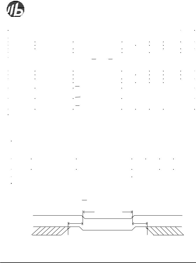
LOW VCC DATA RETENTION WAVEFORM ( CE Controlled )
|
|
|
|
Data Retention Mode |
|
||
Vcc |
Vcc |
|
|
VDR ≥ 1.5V |
Vcc |
||
|
|
|
t CDR |
|
|
|
t R |
|
|
|
|
|
|
≥ Vcc - 0.2V |
|
|
|
|
VIH |
|
CE |
VIH |
|
CE |
|||||||
R0201-BS62LV256 |
3 |
Revision 2.2 |
|
April 2001 |
|
|
|
|
|
|
|
|
|
BSI |
|
|
|
|
|
|
|
|
|
|
|
|
|
|
|
|
|
|
|
|
|
|
|
|
|
|
BS62LV256 |
|||||||||||||||||
|
AC TEST CONDITIONS |
|
|
|
|
|
|
|
|
|
|
|
|
|
|
|
|
|
|
|
|
|
|
|
|
KEY TO SWITCHING WAVEFORMS |
|||||||||||||||||||||||||||
|
|
|
|
|
|
|
|
|
|
|
|
|
|
|
|
|
|
|
|
|
|
|
|
|
|
|
|
|
|
|
|
|
|
|
|
|
|
|
|
|
|
|
|
|
|
|
|
|
|
|
|
||
|
|
Input Pulse Levels |
|
|
|
|
|
|
|
|
|
|
Vcc/0V |
|
|
|
|
|
|
|
|
|
|
|
|
|
|
||||||||||||||||||||||||||
|
|
Input Rise and Fall Times |
|
5ns |
|
|
|
|
|
|
|
|
|
|
|
|
|
|
|
|
|
|
|
WAVEFORM |
INPUTS |
OUTPUTS |
|
||||||||||||||||||||||||||
|
|
Input and Output |
|
|
|
|
|
|
|
|
|
|
|
|
|
|
|
|
|
|
|
|
|
|
|
|
|
|
|
|
|
|
|
|
|
|
|
|
MUST BE |
MUST BE |
|
||||||||||||
|
|
Timing Reference Level |
|
0.5Vcc |
|
|
|
|
|
|
|
|
|
|
|
|
|||||||||||||||||||||||||||||||||||||
|
|
|
|
|
|
|
|
|
|
|
|
|
|
STEADY |
STEADY |
|
|||||||||||||||||||||||||||||||||||||
|
|
|
|
|
|
|
|
|
|
|
|
|
|
|
|
|
|
|
|
|
|
|
|
|
|
|
|
|
|
|
|
|
|
|
|
|
|
|
|
|
|
|
|
|
|
|
|
|
|
|
|
||
|
|
|
|
|
|
|
|
|
|
|
|
|
|
|
|
|
|
|
|
|
|
|
|
|
|
|
|
|
|
|
|
|
|
|
|
|
|
|
|
|
|
|
|
|
|
|
|
|
|
|
|||
|
|
|
|
|
|
|
|
|
|
|
|
|
|
|
|
|
|
|
|
|
|
|
|
|
|
|
|
|
|
|
|
|
|
|
|
|
|
|
|
|
|
|
|
|
|
|
|
|
|
|
MAY CHANGE |
WILL BE |
|
|
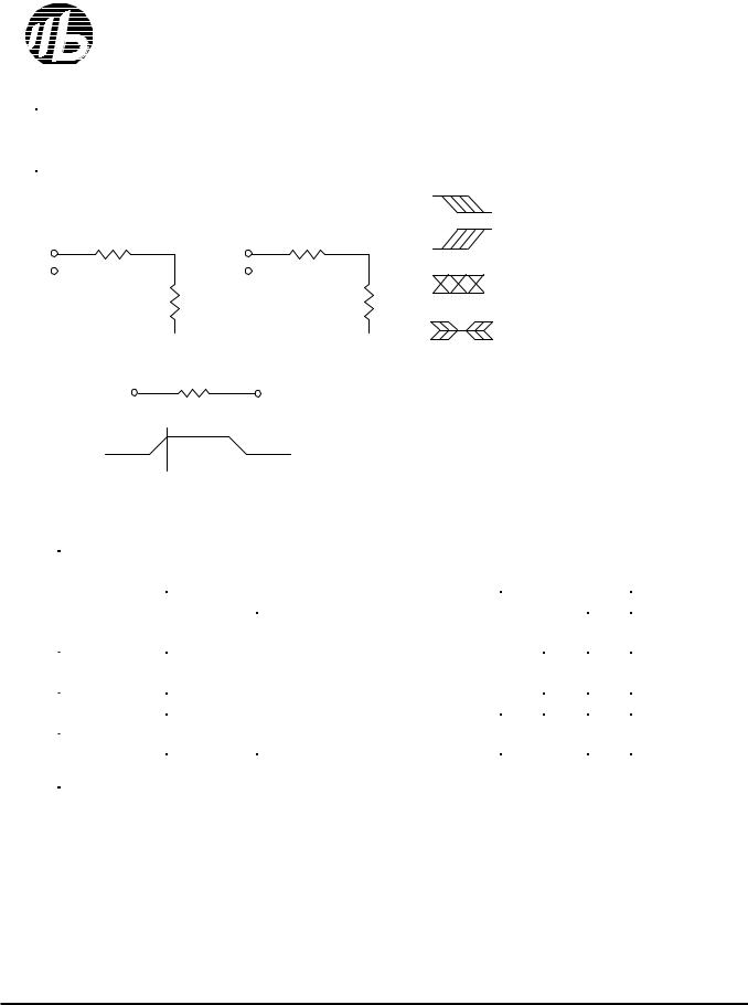
AC TEST LOADS AND WAVEFORMS |
|
|
|
|
|
|
|
|
|
|
|
FROM H TO L |
CHANGE |
|
||||||||||||||||||||||||||||||||||||||
|
|
|
|
|
|
|
|
|
|
|
|
|
FROM H TO L |
|
|||||||||||||||||||||||||||||||||||||||
|
|
|
|
|
|
|
|
|
|
|
|
|
|
|
|
|
|
|
|
|
|
|
|
|
|
|
|
|
|
|
|
|
|
|
|
|
|
|
|
|
|
|
|
|
|
|
|
|
|
|
|
|
|
|
|
|
|
|
|
|
|
|
|
|
|
1269 Ω |
|
|
|
|
|
|
|
|
|
|
|
|
|
|
|
1269 |
Ω |
|
|
MAY CHANGE |
WILL BE |
|
|||||||||||||||||||
3.3V |
|
|
|
|
|
|
|
|
|
|
|
|
|
|
|
|
|
|
3.3V |
|
|
FROM L TO H |
CHANGE |
|
|||||||||||||||||||||||||||||
|
|
|
|
|
|
|
|
|
|
|
|
|
|
|
|
|
|
|
|
|
|
|
|
|
|
|
|
|
|
|
|
|
|
|
|
|
|
|
|
|
|
|
|||||||||||
|
|
|
|
|
|
|
|
|
|
|
|
|
|
|
|
|
|
|
|
|
|
|
|
|
|
|
|
|
|
|
|
|
|
|
|
|
|
|
|
|
|
|
FROM L TO H |
|
|||||||||
OUTPUT |
|
|
|
|
|
|
|
|
|
|
|
|
|
|
|
|
|
|
|
|
OUTPUT |
|
|
|
|
|
|
|
|
|
|
|
|
|
|
|
|
|
|
|
|
|
DON ,T CARE: |
|
|||||||||
|
|
|
|
|
|
|
|
|
|
|
|
|
|
|
|
|
|
|
|
|
|
|
|
|
|
|
|
|
|
|
|
|
|
|
|
|
|
|
|
|
CHANGE : |
|
|||||||||||
|
|
|
|
|
|
|
|
|
|
|
|
|
|
|
|
|
|
|
|
|
|
|
|
|
|
|
|
|
|
|
|
|
|
|
|
|
|
|
|||||||||||||||
|
|
|
|
|
|
|
|
|
|
|
|
100PF |
|
|
|
|
|
|
|
|
|
|
|
|
|
|
|
|
|
|
|
|
|
|
|
|
5PF |
|
|
|
|
|
|
|
|
|
|
|
ANY CHANGE |
STATE |
|
||
|
|
|
|
|
|
|
|
|
|
|
|
|
|
|
|
|
|
|
|
|
|
|
|
|
|
|
|
|
|
|
|
|
|
|
|
|
|
|
|
|
|
|
|
|
|
|
|
||||||
|
INCLUDING |
|
|
|
|
|
1404 |
|
Ω |
|
INCLUDING |
|
|
|
1404 Ω |
|
|
PERMITTED |
UNKNOWN |
|
|||||||||||||||||||||||||||||||||
|
JIG AND |
|
|
|
|
|
|
|
JIG AND |
|
|
|
|
|
DOES NOT |
CENTER |
|
||||||||||||||||||||||||||||||||||||
|
SCOPE |
|
|
|
|
|
|
|
|
|
|
|
|
|
|
|
|
|
|
|
|
|
|
SCOPE |
|
|
|
|
|
|
|
|
|
|
|
|
|
|
|
||||||||||||||
|
|
|
|
|
|
|
|
|
|
|
|
|
|
|
|
|
|
|
|
|
|
|
|
|
|
|
|
|
|
|
|
|
|
|
|
|
|
|
|
|
|
|
|
|
|
|
|
|
|
|
APPLY |
LINE IS HIGH |
|
|
|
|
|
|
|
|
|
|
|
|
|
|
|
|
|
|
|
|
|
|
|
|
|
|
|
|
|
|
|
|
|
|
|
|
|
|
|
|
|
|
|
|
|
|
|
|
|
|
|
|
|
||
|
|
|
|
|
|
|
|
|
|
|
|
FIGURE 1A |
|
|
|
|
|
|
|
|
|
|
|
|
|
|
FIGURE 1B |
|
|
|
IMPEDANCE |
|
|||||||||||||||||||||
|
|
|
|
|
|
|
|
|
|
|
|
|
THEVENIN EQUIVALENT |
|
|
|
|
|
|
|
|
|
|
|
|
”OFF ”STATE |
|
||||||||||||||||||||||||||
|
|
|
|
|
|
|
|
|
|
|
|
|
|
|
|
|
|
|
|
|
|
|
|
|
|
|
|||||||||||||||||||||||||||
|
|
|
|
OUTPUT |
|
|
|
|
|
667 Ω |
|
|
|
|
|
|
|
1.73V |
|
|
|
|
|
|
|
|
|
|
|
|
|
|
|||||||||||||||||||||
|
|
|
|
|
|
|
|
|
|
|
|
|
|
|
|
|
|
|
|
|
|
|
|
|
|
|
|
|
|
|
|
|
|
|
|||||||||||||||||||
|
|
|
|
|
|
|
|
|
|
|
|
|
|
|
ALL INPUT PULSES |
|
|
|
|
|
|
|
|
|
|
|
|
|
|
|
|
|
|
|
|
|
|
|
|
||||||||||||||
|
|
|
|
Vcc |
|
|
|
|
|
|
|
|
|
|
|
|
|
|
|
|
|
|
|
|
|
|
10% |
|
|
|
|
|
|
|
|
|
|
|
|
|
|
|
|
|
|
|
|
|
|||||
|
|
|
|
|
|
|
|
|
|
|
|
|
|
|
|
|
|
|
|
|
|
|
|
|
|
|
|
|
|
|
|
|
|
|
|
|
|
|
|
|
|
|
|
|
|
|
|||||||
|
|
|
|
10% |
|
|
|
90% 90% |
|
|
|
|
|
|
|
|
|
|
|
|
|
|
|
|
|
|
|
|
|
|
|
|
|
|
|||||||||||||||||||
|
|
|
|
GND |
|
|
|
|
|
|
|
|
|
|
|
|
|
|
|
|
|
|
|
|
|
|
|
|
|
|
|
|
|||||||||||||||||||||
|
|
|
|
|
|
|
|
|
|
|
|
|
|
|
|
|
|
|
|
|
|
|
|
|
|
|
|
|
|
|
|
|
|
|
|
|
|
|
|
|
|
|
|
|
|
|
|
|
|||||
|
|
|
|
|
|
|
→ |
|
|
|
|
← |
→ |
|
|
|
|
← 5ns |
|
|
|
|
|
|
|
|
|
|
|
|
|
|
|||||||||||||||||||||
|
|
|
|
|
|
|
|
|
|
|
|
|
|
|
|
|
|
|
|
|
|
|
|
|
|
|
|
|
|
|
|
|
|
||||||||||||||||||||
|
|
|
|
|
|
|
|
|
|
|
|
|
|
|
|
|
|
|
|
|
|
|
|
|
|
||||||||||||||||||||||||||||
FIGURE 2
AC ELECTRICAL CHARACTERISTICS ( TA =0oC to + 70oC and Vcc=3.0V) READ CYCLE
JEDEC |
PARAMETER |
|
|
BS62LV256 |
|
||
PARAMETER |
DESCRIPTION |
|
UNIT |
||||
NAME |
MIN. |
|
TYP. |
MAX. |
|||
NAME |
|
|
|
||||
|
|
|
|
|
|
|
|
tAVAX |
tRC |
Read Cycle Time |
70 |
|
-- |
-- |
ns |
tAVQV |
tAA |
Address Access Time |
-- |
|
-- |
70 |
ns |
tELQV |
tACS |
Chip Select Access Time |
-- |
|
-- |
70 |
ns |
tGLQV |
tOE |
Output Enable to Output Valid |
-- |
|
-- |
50 |
ns |
tELQX |
tCLZ |
Chip Select to Output Low Z |
10 |
|
-- |
-- |
ns |
tGLQX |
tOLZ |
Output Enable to Output in Low Z |
10 |
|
-- |
-- |
ns |
tEHQZ |
tCHZ |
Chip Deselect to Output in High Z |
0 |
|
-- |
35 |
ns |
tGHQZ |
tOHZ |
Output Disable to Output in High Z |
0 |
|
-- |
30 |
ns |
tAXOX |
tOH |
Output Disable to Output Address Change |
10 |
|
-- |
-- |
ns |
R0201-BS62LV256 |
4 |
Revision 2.2 |
|
April 2001 |
 Loading...