

Page 1
CB4055
Manual
rev. 1.0
Beckhoff Automation GmbH phone: +49 (0) 52 46/963-0
Eiserstr. 5 fax: +49 (0) 52 46/963-198
33415 Verl email: info@beckhoff.de
Germany web: www.beckhoff.de
Page 2

Page 3

Contents
Contents
0 Document History ................................................................................................................................. 5
1 Introduction ........................................................................................................................................... 6
1.1 Notes on the Documentation ......................................................................................................... 6
1.1.1 Liability Conditions ................................................................................................................ 6
1.1.2 Copyright ............................................................................................................................... 6
1.2 Safety Instructions ......................................................................................................................... 7
1.2.1 Disclaimer .............................................................................................................................. 7
1.2.2 Description of Safety Symbols .............................................................................................. 7
1.3 Essential Safety Measures ............................................................................................................ 8
1.3.1 Operator's Obligation to Exercise Diligence .......................................................................... 8
1.3.2 National Regulations Depending on the Machine Type ........................................................ 8
1.3.3 Operator Requirements ......................................................................................................... 8
1.4 Functional Range .......................................................................................................................... 9
2 Overview ............................................................................................................................................. 10
2.1 Features ...................................................................................................................................... 10
2.2 Specifications and Documents .................................................................................................... 12
3 Connectors ......................................................................................................................................... 14
3.1 Connector Map ............................................................................................................................ 15
3.2 Power Supply .............................................................................................................................. 16
3.3 System/SM-Bus ........................................................................................................................... 17
3.4 Memory ....................................................................................................................................... 18
3.5 PCI/104-Express Bus .................................................................................................................. 21
3.6 DVI/HDMI .................................................................................................................................... 23
3.7 DisplayPort .................................................................................................................................. 24
3.8 VGA ............................................................................................................................................. 25
3.9 LCD ............................................................................................................................................. 26
3.10 USB ............................................................................................................................................. 28
3.11 LAN.............................................................................................................................................. 29
3.12 Audio ........................................................................................................................................... 30
3.13 SATA Interfaces .......................................................................................................................... 31
3.14 COM1 and COM2 ........................................................................................................................ 32
3.15 GPIO............................................................................................................................................ 33
3.16 Monitoring Functions ................................................................................................................... 34
4 Status LEDs ........................................................................................................................................ 35
4.1 HD LED ....................................................................................................................................... 35
4.2 RGB LED ..................................................................................................................................... 36
5 BIOS Settings ..................................................................................................................................... 37
5.1 Remarks for Setup Use ............................................................................................................... 37
5.2 Main ............................................................................................................................................. 38
5.3 Advanced .................................................................................................................................... 40
5.3.1 PCI Subsystem Settings...................................................................................................... 41
5.3.2 ACPI Settings ...................................................................................................................... 43
5.3.3 CPU Configuration .............................................................................................................. 44
5.3.4 SATA Configuration ............................................................................................................. 46
5.3.5 Power Controller Options .................................................................................................... 47
5.3.6 USB Configuration ............................................................................................................... 48
Beckhoff New Automation Technology CB4055 page 3
Page 4

Contents
5.3.7 Super IO Configuration ........................................................................................................ 49
5.3.8 H/W Monitor ........................................................................................................................ 51
5.3.9 Serial Port Console Redirection .......................................................................................... 53
5.3.10 CPU PPM Configuration...................................................................................................... 55
5.4 Chipset ........................................................................................................................................ 56
5.4.1 PCH-IO Configuration ......................................................................................................... 57
5.4.2 System Agent (SA) Configuration ....................................................................................... 64
5.5 Boot ............................................................................................................................................. 68
5.5.1 CSM Parameters ................................................................................................................. 70
5.6 Security ....................................................................................................................................... 71
5.6.1 Secure Boot Policy .............................................................................................................. 72
5.6.2 Key Management ................................................................................................................ 73
5.7 Save & Exit .................................................................................................................................. 75
5.8 BIOS update ................................................................................................................................ 76
6 Mechanical Drawing ........................................................................................................................... 77
6.1 PCB: Mounting Holes .................................................................................................................. 77
6.2 PCB: Pin 1 Dimensions ............................................................................................................... 78
6.3 PCB: Heat Sink/Die Center ......................................................................................................... 79
7 Technical Data .................................................................................................................................... 80
7.1 Electrical Data ............................................................................................................................. 80
7.2 Environmental Conditions ........................................................................................................... 80
7.3 Thermal Specifications ................................................................................................................ 81
8 Support and Service ........................................................................................................................... 82
8.1 Beckhoff's Branch Offices and Representatives ......................................................................... 82
8.2 Beckhoff Headquarters................................................................................................................ 82
8.2.1 Beckhoff Support ................................................................................................................. 82
8.2.2 Beckhoff Service ................................................................................................................. 82
I Anhang: Post-Codes .......................................................................................................................... 83
II Annex: Resources .............................................................................................................................. 84
IO Range ................................................................................................................................................. 84
Memory Range ....................................................................................................................................... 84
Interrupt ................................................................................................................................................... 84
PCI Devices ............................................................................................................................................ 85
SMB Devices .......................................................................................................................................... 85
page 4 Beckhoff New Automation Technology CB4055
Page 5

Notes on the Documentation Chapter: Document History
0 Document History
Version Changes
0.1 first pre-release
0.2 corrected RAM frequency; explained DP pin 11, minor changes
1.0 first complete version
NOTE
All company names, brand names, and product names referred to in this manual are registered or
unregistered trademarks of their respective holders and are, as such, protected by national and
international law.
Beckhoff New Automation Technology CB4055 page 5
Page 6

Chapter: Introduction Notes on the Documentation
1 Introduction
1.1 Notes on the Documentation
This description is only intended for the use of trained specialists in control and automation engineering
who are familiar with the applicable national standards. It is essential that the following notes and
explanations are followed when installing and commissioning these components.
1.1.1 Liability Conditions
The responsible staff must ensure that the application or use of the products described satisfy all the
requirements for safety, including all the relevant laws, regulations, guidelines and standards.
The documentation has been prepared with care. The products described are, however, constantly under
development. For that reason the documentation is not in every case checked for consistency with
performance data, standards or other characteristics. None of the statements of this manual represents a
guarantee (Garantie) in the meaning of § 443 BGB of the German Civil Code or a statement about the
contractually expected fitness for a particular purpose in the meaning of § 434 par. 1 sentence 1 BGB. In
the event that it contains technical or editorial errors, we retain the right to make alterations at any time
and without warning. No claims for the modification of products that have already been supplied may be
made on the basis of the data, diagrams and descriptions in this documentation.
1.1.2 Copyright
© This documentation is copyrighted. Any reproduction or third party use of this publication, whether in
whole or in part, without the written permission of Beckhoff Automation GmbH, is forbidden.
page 6 Beckhoff New Automation Technology CB4055
Page 7
Safety Instructions Chapter: Introduction
1.2 Safety Instructions
Please consider the following safety instructions and descriptions. Product specific safety instructions are
to be found on the following pages or in the areas mounting, wiring, commissioning etc.
1.2.1 Disclaimer
All the components are supplied in particular hardware and software configurations appropriate for the
application. Modifications to hardware or software configurations other than those described in the
documentation are not permitted, and nullify the liability of Beckhoff Automation GmbH.
1.2.2 Description of Safety Symbols
The following safety symbols are used in this documentation. They are intended to alert the reader to the
associated safety instructions.
ACUTE RISK OF INJURY!
If you do not adhere to the safety advise next to this symbol, there is immediate danger to life and health
of individuals!
RISK OF INJURY!
If you do not adhere to the safety advise next to this symbol, there is danger to life and health of
individuals!
HAZARD TO INDIVIDUALS, ENVIRONMENT, DEVICES, OR DATA!
If you do not adhere to the safety advise next to this symbol, there is obvious hazard to individuals, to
environment, to materials, or to data.
NOTE OR POINTER
This symbol indicates information that contributes to better understanding.
Beckhoff New Automation Technology CB4055 page 7
Page 8

Chapter: Introduction Essential Safety Measures
1.3 Essential Safety Measures
1.3.1 Operator's Obligation to Exercise Diligence
The operator must ensure that
o the product is only used for its intended purpose
o the product is only operated in sound condition and in working order
o the instruction manual is in good condition and complete, and always available for reference at the
location where the products are used
o the product is only used by suitably qualified and authorised personnel
o the personnel is instructed regularly about relevant occupational safety and environmental protection
aspects
o the operating personnel is familiar with the operating manual and in particular the safety notes
contained herein
1.3.2 National Regulations Depending on the Machine Type
Depending on the type of machine and plant in which the product is used, national regulations governing
the controllers of such machines will apply, and must be observed by the operator. These regulations
cover, amongst other things, the intervals between inspections of the controller. The operator must initiate
such inspections in good time.
1.3.3 Operator Requirements
o Read the operating instructions
All users of the product must have read the operating instructions for the system they work with.
o System know-how
All users must be familiar with all accessible functions of the product.
page 8 Beckhoff New Automation Technology CB4055
Page 9

Functional Range Chapter: Introduction
1.4 Functional Range
NOTE
The descriptions contained in the present documentation represent a detailed and extensive product
description. As far as the described motherboard was acquired as an integral component of an Industrial
PC from Beckhoff Automation GmbH, this product description shall be applied only in limited scope. Only
the contractually agreed specifications of the corresponding Industrial PC from Beckhoff Automation
GmbH shall be relevant. Due to several models of Industrial PCs, variations in the component placement
of the motherboards are possible. Support and service benefits for the built-in motherboard will be
rendered by Beckhoff Automation GmbH exclusively as specified in the product description (inclusive
operation system) of the particular Industrial PC.
Beckhoff New Automation Technology CB4055 page 9
Page 10
Chapter: Overview Features
2 Overview
2.1 Features
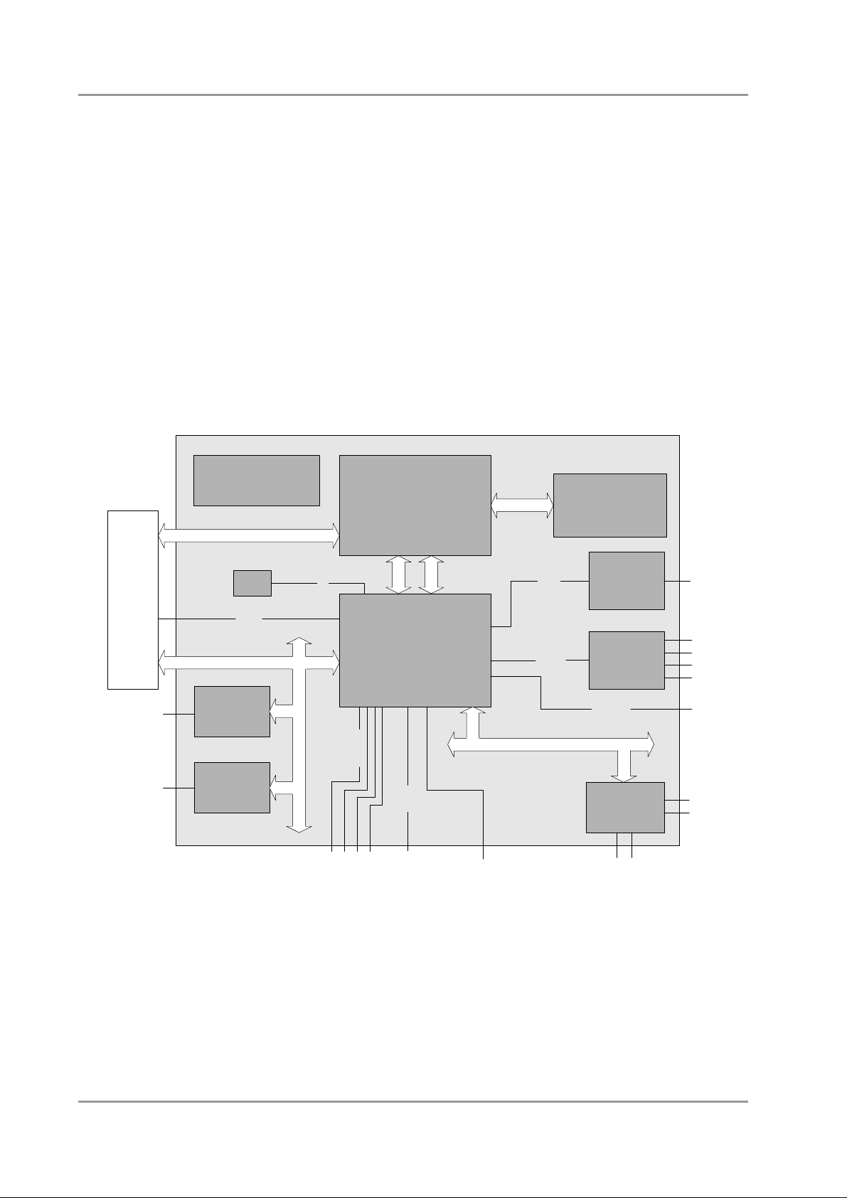
The CB4055 is a highly complex computer motherboard in the PC/104™ form factor, complying with the
state-of-the-art "PCIe/104™" standard. It's based on Intel® CPUs of the 2nd Generation Core™ and
Celeron® families (BGA, embedded) combined with the QM67 PCH. Modern DDR3 technology provides
top-notch memory performance, accomodating up to 4 GByte of RAM (DDR3-1066/1333/1600) via
SO-DIMM204. PCI-Express is available through the PCI/104-Express Type 1 connector, offering one x16
connection and four x1 lanes for connecting all kinds of expansion cards in a PCIe/104™ stack-down
fashion. For connecting graphics devices, several interfaces are available: CRT, LVDS, HDMI,
DisplayPort. Additional interfaces include two serial ports, two Gigabit Ethernet interfaces (LAN), two
SATA channels (up to 6Gb/s), an audio interface (HDA 7.1), and ten USB channels. There are also 16
discrete programmable GPIO signals available.
Power VCCCore; VTT;
PCIe x16
DDRVTT, GFXVCC
1,05V; 1,5V; 1,8V; 3,3V
PCIe (x16) / PEG
Intel®:
Core™ i7-2715QE,
Core™ i7-2655LE,
Celeron® 827E
MEMORY
SO-DIMM204
DDR3-1066/1333
(dual channel)
FDI
USB9-10
PCIe/104 connector (type 1)
PCIe x1
4x
LAN1
LAN2
USB 2.0
PCIe (x1)
Intel®
82579L
Intel®
82574L
BIOS
SPI
Intel® QM67 PCH
18/24/36/48
CRT
LVDS
DP/HDMI
DVI/HDMI
ddd
USB 2.0
USB1-8
DMI
SMBus
SMBus
HDA Link
LPC
o Processor Intel® Core™ i7-2715QE, i7-2655LE, or Celeron® 827E
o Chipset Intel® QM67 PCH
o SO-DIMM204 socket for one DDR3-1066/1333/1600 module of up to 4 GByte
o Two serial interfaces COM1-2
o Two LAN interfaces Ethernet 10/100/1000 (Base-T)
o Two SATA channels (1.5/3/6 Gb/s)
o PS2 keyboard / mouse interface
NXP®
PCA9535
RealTek®
RealTek®
ALC889
ALC889
1.5/3/6 Gb/s
SMSC®
SCH3114
16x GPIO
SPDIF i/o
7.1 Audio
AUX l/r
MIC 1/2
2x SATA
KB
MS
FAN 1-3
COM1-2
page 10 Beckhoff New Automation Technology CB4055
Page 11

Features Chapter: Overview
o Ten USB 2.0 interfaces (two on PCI104-Express connector)
o BIOS AMI® Aptio
o DisplayPort interface
o HDMI interface
o CRT connection
o LCD connection via LVDS 18/24bit (dual pixel)
o HDA compatible sound controller with SPDIF in and out
o RTC with external CMOS battery
o PCI-Express bus via PCI/104-Express connector (type 1, one x16, four x1 lanes)
o 16x GPIO
o 5V and 12V supply voltage
o Size: 96 mm x 90 (115.5) mm
Beckhoff New Automation Technology CB4055 page 11
Page 12

Chapter: Overview Specifications and Documents
2.2 Specifications and Documents
In making this manual and for further reading of technical documentation, the following documents,
specifications and web-pages were used and are recommended.
§ PC/104™ Specification
Version 2.5
www.pc104.org
§ PC/104-Plus™ Specification
Version 2.0
www.pc104.org
§ PCI/104-Express™ Specification
Version 2.0
www.pc104.org
§ PCI Specification
Version 2.3 and 3.0
www.pcisig.com
§ ACPI Specification
Version 3.0
www.acpi.info
§ ATA/ATAPI Specification
Version 7 Rev. 1
www.t13.org
§ USB Specifications
www.usb.org
§ SM-Bus Specification
Version 2.0
www.smbus.org
§ Intel® Chipset Description
Intel® 6 Series Chipset Datasheet
www.intel.com
§ Intel® Chip Description
2nd Generation Core™ Processor Family Datasheet
www.intel.com
§ SMSC® Chip Description
SCH3114 Datasheet
www.smsc.com
(NDA required)
§ Intel® Chip Description
82574L Datasheet
www.intel.com
§ Intel® Chip Description
82579L Datasheet
www.intel.com
§ Realtek® Chip Description
ALC885/889 Datasheet
www.realtek.com.tw
page 12 Beckhoff New Automation Technology CB4055
Page 13

Specifications and Documents Chapter: Overview
§ Chrontel® Chip Description
Chrontel 7318C Datasheet
www.chrontel.com
§ American Megatrends®
Aptio™ Text Setup Environment (TSE) User Manual
www.ami.com
§ American Megatrends®
Aptio™ 4.x Status Codes
www.ami.com
Beckhoff New Automation Technology CB4055 page 13
Page 14

Chapter: Connectors Specifications and Documents
3 Connectors
This section describes all the connectors found on the CB4055.
CAUTION
For most interfaces, the cables must meet certain requirements. For instance, USB 2.0 requires twisted
and shielded cables to reliably maintain full speed data rates. Restrictions on maximum cable length are
also in place for many high speed interfaces and for power supply. Please refer to the respective
specifications and use suitable cables at all times.
page 14 Beckhoff New Automation Technology CB4055
Page 15
Connector Map Chapter: Connectors
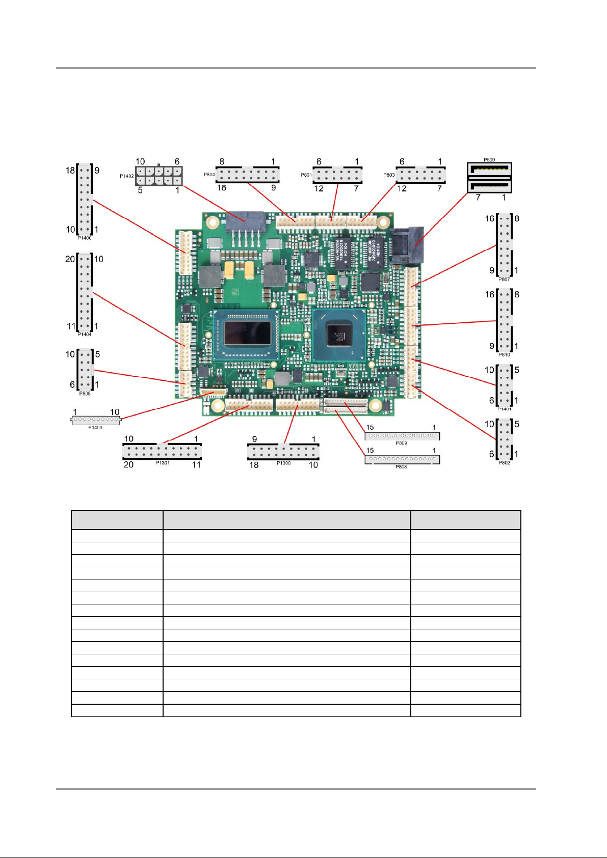
3.1 Connector Map
Please use the connector map below for quick reference. Only connectors on the component side are
shown. For more information on each connector refer to the table below.
Ref-No. Function Page
P500 "SATA Interfaces" p. 31
U600* "Memory" p. 18
P801/3 "LAN" p. 29
P802/5 "COM1 and COM2" p. 32
P804 "Audio" p. 30
P807/10 "USB" p. 28
P808/9 "LCD" p. 26
P1200* "PCI/104-Express Bus" p. 21
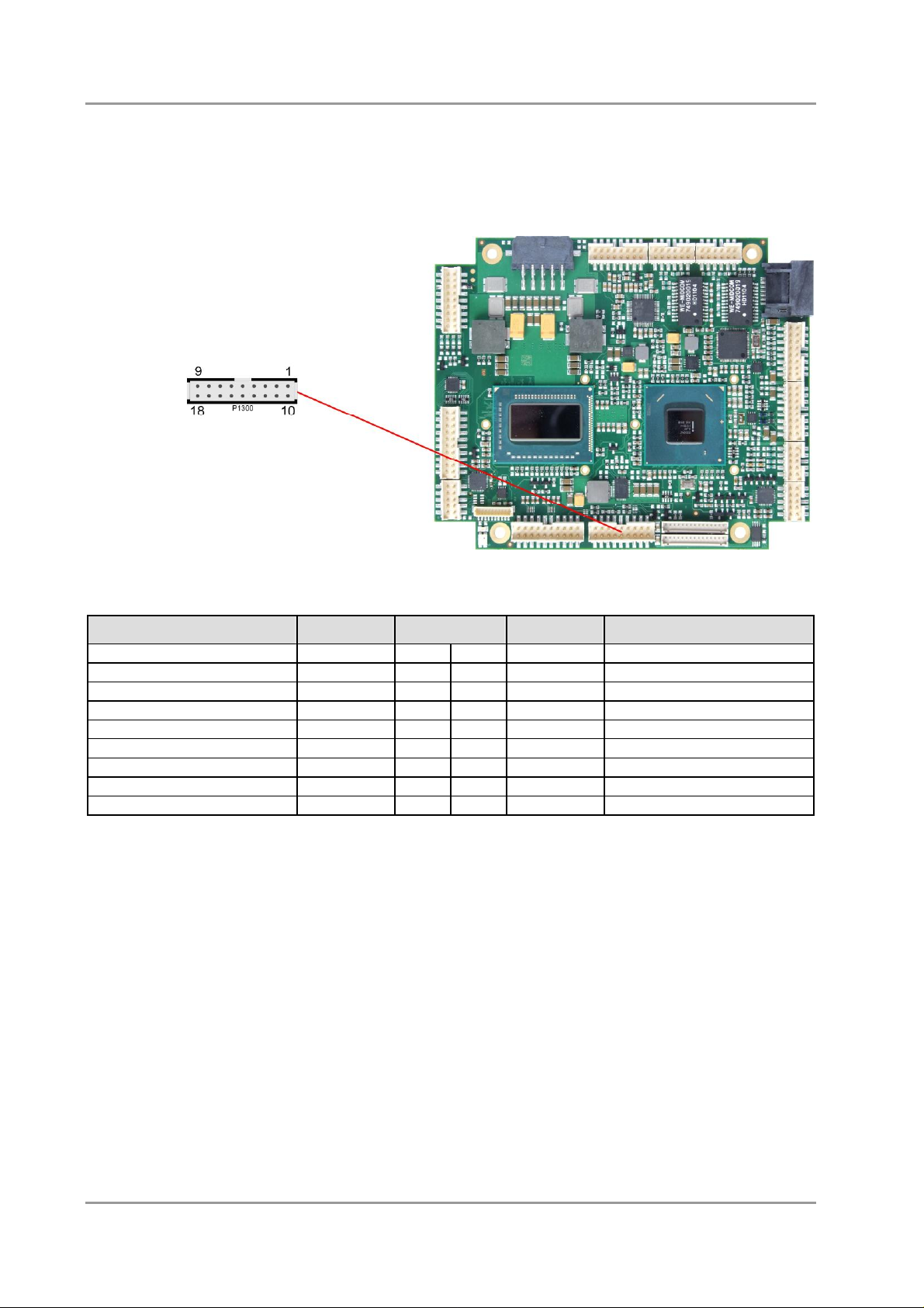
P1300 "DVI/HDMI" p. 23
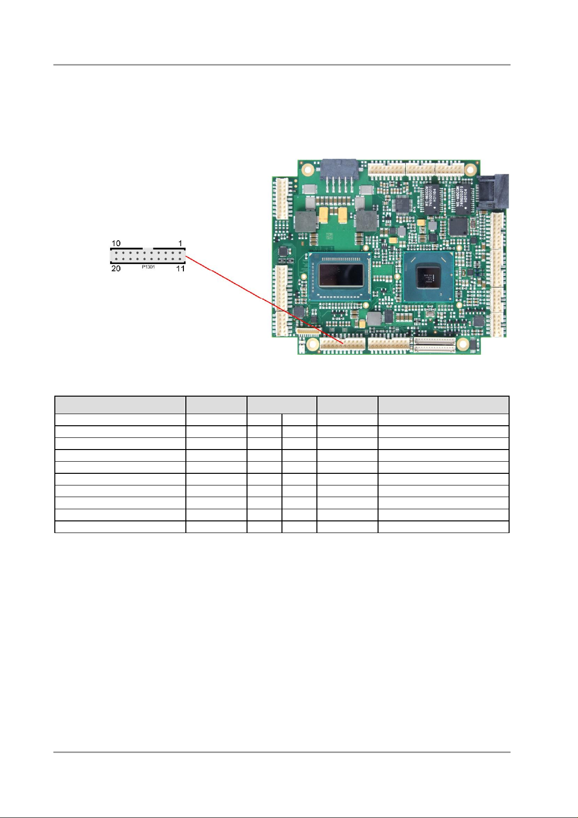
P1301 "DisplayPort" p. 24
P1400 "System/SM-Bus" p. 17
P1401 "VGA" p. 25
P1402 "Power Supply" p. 16
P1403 "Monitoring Functions" p. 34
P1404 "GPIO" p. 33
* not in the picture above (cf. bottom side of board)
Beckhoff New Automation Technology CB4055 page 15
Page 16
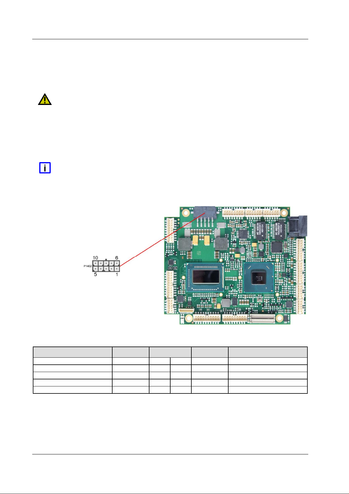
Chapter: Connectors Power Supply
3.2 Power Supply
The power supply of the hardware module is realized via a 2x5-pin connector (Molex PS 43045-10xx,
mating connector: Molex PS 43025-10xx). Both 5V VCC/SVCC and 12V need to be provided. The 12V
input can optionally be tied to 5V if 12V is not required by attached peripherals. It cannot, however, be left
unconnected.
CAUTION
The CB4055 includes circuitry that will notify an intelligent power supply to shut down if the processor
reaches a critical temperature. This is achieved by deasserting the (low-active) PS_ON# signal found on
the SM-Bus connector. When PS_ON# is no longer pulled low, an intelligent power supply would take this
as a signal to shut down power. For this to work, PS_ON# must be connected to the power supply's
PS_ON input. If PS_ON# is not otherwise connected, the CB4055 can be damaged beyond repair if a
thermal shutdown event occurs. In rare instances, if power is not shut down, the board will continue to
heat up until failure occurs.
NOTE
Since this is a 90 degree connector, the symbol in the drawing below represents the connector face as
seen from the side (PCB on bottom) rather than from above.
Description Name Pin Name Description
12 volt supply 12V 1 6 12V 12 volt supply
ground GND 2 7 GND ground
ground GND 3 8 SVCC standby-supply 5V
ground GND 4 9 GND ground
5 volt supply VCC 5 10 VCC 5 volt supply
page 16 Beckhoff New Automation Technology CB4055
Page 17
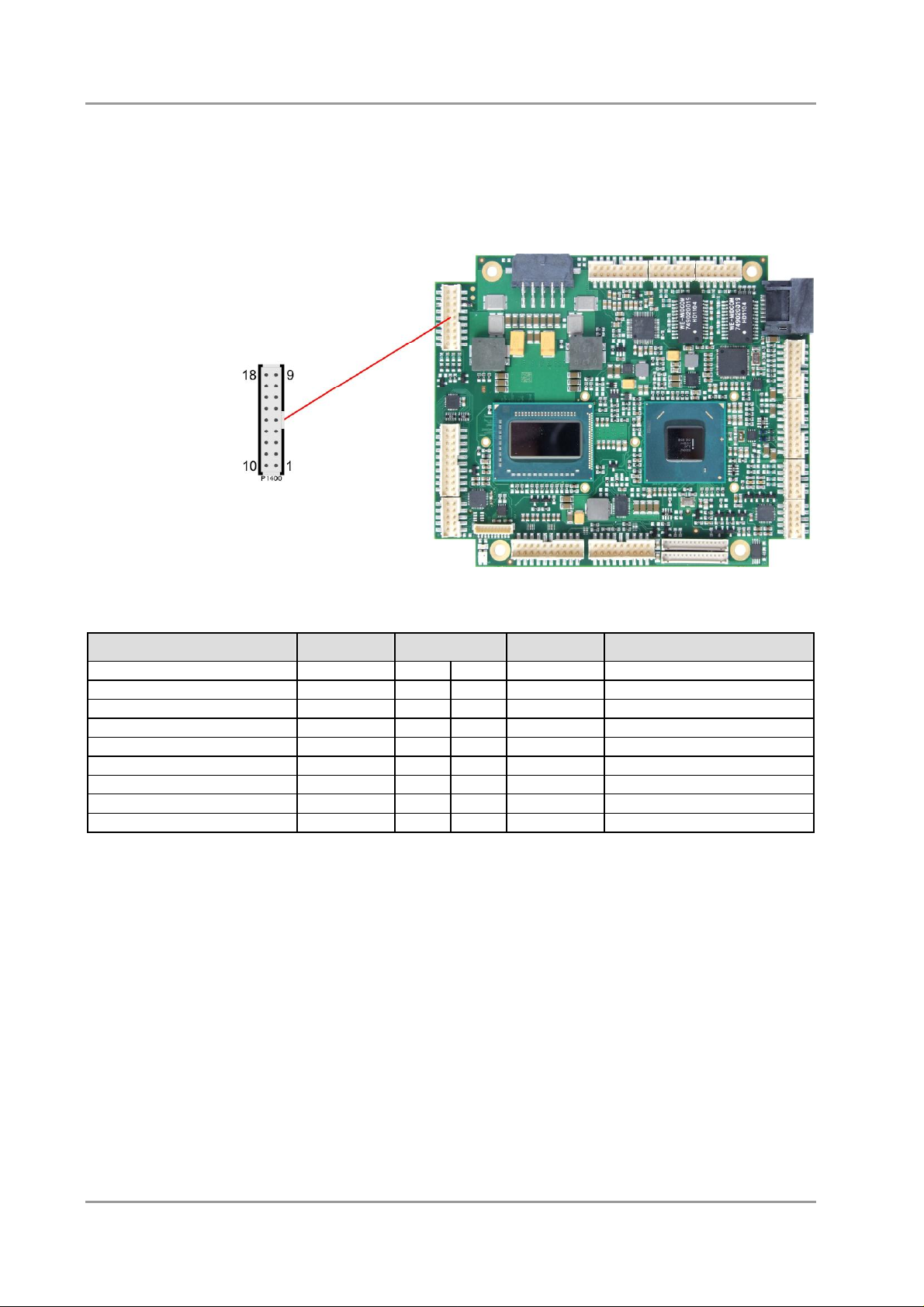
System/SM-Bus Chapter: Connectors
3.3 System/SM-Bus
Both SM-Bus signals, and signals for PS/2 keyboard, PS/2 mouse and speaker are provided through a
2x9pin connector (FCI 98424-G52-18LF, mating connector e.g. FCI 90311-018LF). For the #PSON
signal, please refer to the cautionary note in the chapter "Power Supply" (p. 16).
Pinout 2x9pin connector:
Description Name Pin Name Description
speaker to 5V SPEAKER 1 10 GND ground
reset to ground RSTBTN# 2 11 N/C reserved
keyboard data KDAT 3 12 KCLK keyboard clock
mouse data MDAT 4 13 MCLK mouse clock
battery BATT 5 14 VCC 5 volt supply
power supply on PS-ON# 6 15 SMBCLK SMB clock
standby supply 3.3V S3.3V 7 16 SMBDAT SMB data
power button PWRBTN# 8 17 SMBALERT# SMB alert
ground GND 9 18 3.3V 3.3 volt supply
Beckhoff New Automation Technology CB4055 page 17
Page 18
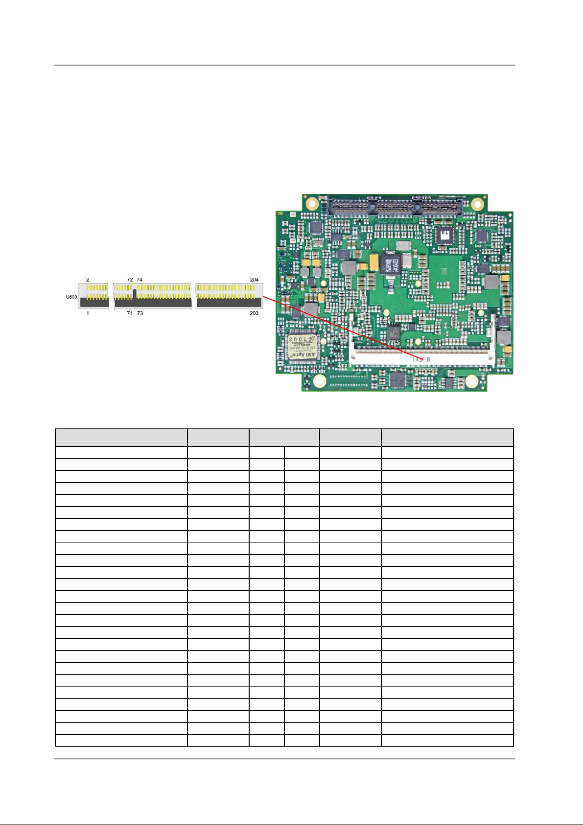
Chapter: Connectors Memory
3.4 Memory
There is one conventional SO-DIMM204 socket available to equip the board with memory
(DDR3-1066/1333/1600). It is located on the bottom side of the board. For technical and mechanical
reasons it is possible that particular memory modules cannot be employed. Please ask your sales
representative for recommended memory modules.
With currently available SO-DIMM modules a memory extension up to 4 GByte is possible. The timing
parameters for different memory modules are automatically set by BIOS.
Description Name Pin Name Description
memory reference current REF-DQ 1 2 GND ground
ground GND 3 4 DQ4 data 4
data 0 DQ0 5 6 DQ5 data 5
data 1 DQ1 7 8 GND ground
ground GND 9 10 DQS0# data strobe 0 data mask 0 DM0 11 12 DQS0 data strobe 0 +
ground GND 13 14 GND ground
data 2 DQ2 15 16 DQ6 data 6
data 3 DQ3 17 18 DQ7 data 7
ground GND 19 20 GND ground
data 8 DQ8 21 22 DQ12 data 12
data 9 DQ9 23 24 DQ13 data 13
ground GND 25 26 GND ground
data strobe 1 - DQS1# 27 28 DM1 data mask 1
data strobe 1 + DQS1 29 30 RESET# Reset
ground GND 31 32 GND ground
data 10 DQ10 33 34 DQ14 data 14
data 11 DQ11 35 36 DQ15 data 15
ground GND 37 38 GND ground
data 16 DQ16 39 40 DQ20 data 20
data 17 DQ17 41 42 DQ21 data 21
ground GND 43 44 GND ground
data strobe 2 - DQS2# 45 46 DM2 data mask 2
data strobe 2 + DQS2 47 48 GND ground
ground GND 49 50 DQ22 data 22
page 18 Beckhoff New Automation Technology CB4055
Page 19

Memory Chapter: Connectors
Description Name Pin Name Description
data 18 DQ18 51 52 DQ23 data 23
data 19 DQ19 53 54 GND ground
ground GND 55 56 DQ28 data 28
data 24 DQ24 57 58 DQ29 data 29
data 25 DQ25 59 60 GND ground
ground GND 61 62 DQS3# data strobe 3 data mask 3 DQM3 63 64 DQS3 data strobe 3 +
ground GND 65 66 GND ground
data 26 DQ26 67 68 DQ30 data 30
data 27 DQ27 69 70 DQ31 data 31
ground GND 71 72 GND ground
clock enables 0 CKE0 73 74 CKE1 clock enables 1
1.5 volt supply 1.5V 75 76 1.5V 1.5 volt supply
reserved N/C 77 78 (A15) reserved
SDRAM bank 2 BA2 79 80 A14 address 14
1.5 volt supply 1.5V 81 82 1.5V 1.5 volt supply
address 12 (burst chop) A12/BC# 83 84 A11 address 11
address 9 A9 85 86 A7 address 7
1.5 volt supply 1.5V 87 88 1.5V 1.5 volt supply
address 8 A8 89 90 A6 address 6
address 5 A5 91 92 A4 address 4
1.5 volt supply 1.5V 93 94 1.5V 1.5 volt supply
address 3 A3 95 96 A2 address 2
address 1 A1 97 98 A0 address 0
1.5 volt supply 1.5V 99 100 1.5V 1.5 volt supply
Clock 0 + CK0 101 102 CK1 clock 1 +
Clock 0 - CK0# 103 104 CK1# clock 1 -
1.5 volt supply 1.5V 105 106 1.5V 1.5 volt supply
address 10 (auto precharge) A10/AP 107 108 BA1 SDRAM bank 1
SDRAM Bank 0 BA0 109 110 RAS# row address strobe
1.5 volt supply 1.5V 111 112 1.5V 1.5 volt supply
write enable WE# 113 114 S0# chip select 0
column address strobe CAS# 115 116 ODT0 on die termination 0
1.5 volt supply 1.5V 117 118 1.5V 1.5 volt supply
address 13 A13 119 120 ODT1 on die termination 1
Chip Select 1 S1# 121 122 N/C reserved
1.5 volt supply 1.5V 123 124 1.5V 1.5 volt supply
reserved (TEST) 125 126 REF-CA reference current
ground GND 127 128 GND ground
data 32 DQ32 129 130 DQ36 data 36
data 33 DQ33 131 132 DQ37 data 37
ground GND 133 134 GND ground
data strobe 4 - DQS4# 135 136 DQM4 data mask 4
data strobe 4 + DQS4 137 138 GND ground
ground GND 139 140 DQ38 data 38
data 34 DQ34 141 142 DQ39 data 39
data 35 DQ35 143 144 GND ground
ground GND 145 146 DQ44 data 44
data 40 DQ40 147 148 DQ45 data 45
data 41 DQ41 149 150 GND ground
ground GND 151 152 DQS5# data strobe 5 data mask 5 DQM5 153 154 DQS5 data strobe 5 +
ground GND 155 156 GND ground
data 42 DQ42 157 158 DQ46 data 46
data 43 DQ43 159 160 DQ47 data 47
Beckhoff New Automation Technology CB4055 page 19
Page 20

Chapter: Connectors Memory
Description Name Pin Name Description
ground GND 161 162 GND ground
data 48 DQ48 163 164 DQ52 data 52
data 49 DQ49 165 166 DQ53 data 53
ground GND 167 168 GND ground
data strobe 6 - DQS6# 169 170 DQM6 data mask 6
data strobe 6 DQS6 171 172 GND ground
ground GND 173 174 DQ54 data 54
data 50 DQ50 175 176 DQ55 data 55
data 51 DQ51 177 178 GND ground
ground GND 179 180 DQ60 data 60
data 56 DQ56 181 182 DQ61 data 61
data 57 DQ57 183 184 GND ground
ground GND 185 186 DQS7# data strobe 7 data mask 7 DQM7 187 188 DQS7 data strobe 7 +
ground GND 189 190 GND ground
data 58 DQ58 191 192 DQ62 data 62
data 59 DQ59 193 194 DQ63 data 63
ground GND 195 196 GND ground
SPD address 0 SA0 197 198 EVENT# Event
3.3 volt supply 3.3V 199 200 SDA SMBus data
SPD address 1 SA1 201 202 SCL SMBus clock
termination current VTT 203 204 VTT termination current
page 20 Beckhoff New Automation Technology CB4055
Page 21
PCI/104-Express Bus Chapter: Connectors
3.5 PCI/104-Express Bus
Expansion modules for the PCI-Express bus can be connected to the board using the PCI/104-Express™
connector. This is a "type 1" connector which offers full PCI-Express x16. "Stacking Error" functionality is
available. For specifics, please refer to the PCI/104-Express™ documentation (rev. 2.0).
Description Name Pin Name Description
reserved N/C 1 2 PERST# PCIe reset
3.3 volt supply 3.3V 3 4 3.3V 3.3 volt supply
display data channel clock DDPC-CLK 5 6 N/C reserved
display data channel data DDPC-DAT 7 8 N/C reserved
ground GND 9 10 GND ground
transmit lane 2 + PET2 11 12 PET1 transmit lane 1 +
transmit lane 2 - PET2# 13 14 PET1# transmit lane 1 ground GND 15 16 GND ground
transmit lane 3 + PET3 17 18 PET4 transmit lane 4 +
transmit lane 3 - PET3# 19 20 PET4# transmit lane 4 ground GND 21 22 GND ground
receive lane 2 + PER2 23 24 PER1 receive lane 1 +
receive lane 2 - PER2# 25 26 PER1# receive lane 1 ground GND 27 28 GND ground
receive lane 3 + PER3 29 30 PER4 receive lane 4 +
receive lane 3 - PER3# 31 32 PER4# receive lane 4 ground GND 33 34 GND ground
clock slot 1 + PECLK1 35 36 PECLK0 clock slot 0 +
clock slot 1 - PECLK1# 37 38 PECLK0# clock slot 0 5 volt standby supply SVCC 39 40 SVCC 5 volt standby supply
clock slot 2 + PECLK2 41 42 PECLK3 clock slot 3 +
clock slot 2 - PECLK2# 43 44 PECLK3# clock slot 3 CPU direction CPU_DIR 45 46 PWRGOOD powergood
SMBus data SMBDAT 47 48 PECLKx16 clock x16 slot +
SMBus clock SMBCLK 49 50 PECLKx16# clock x16 slot SMBus alert SMBALERT 51 52 PSON# PSU on
link reactivation PEWAKE# 53 54 PEGENA# PCIe graphics enable
ground GND 55 56 GND ground
Beckhoff New Automation Technology CB4055 page 21
Page 22

Chapter: Connectors PCI/104-Express Bus
Description Name Pin Name Description
x16 transmit lane 8 + PE16T8 57 58 PE16T0 x16 transmit lane 0 +
x16 transmit lane 8 - PE16T8# 59 60 PE16T0# x16 transmit lane 0 ground GND 61 62 GND ground
x16 transmit lane 9 + PE16T9 63 64 PE16T1 x16 transmit lane 1 +
x16 transmit lane 9 - PE16T9# 65 66 PE16T1# x16 transmit lane 1 ground GND 67 68 GND ground
x16 transmit lane 10 + PE16T10 69 70 PE16T2 x16 transmit lane 2 +
x16 transmit lane 10 - PE16T10# 71 72 PE16T2# x16 transmit lane 2 ground GND 73 74 GND ground
x16 transmit lane 11 + PE16T11 75 76 PE16T3 x16 transmit lane 3 +
x16 transmit lane 11 - PE16T11# 77 78 PE16T3# x16 transmit lane 3 ground GND 79 80 GND ground
x16 transmit lane 12 + PE16T12 81 82 PE16T4 x16 transmit lane 4 +
x16 transmit lane 12 - PE16T12# 83 84 PE16T4# x16 transmit lane 4 ground GND 85 86 GND ground
x16 transmit lane 13 + PE16T13 87 88 PE16T5 x16 transmit lane 5 +
x16 transmit lane 13 - PE16T13# 89 90 PE16T5# x16 transmit lane 5 ground GND 91 92 GND ground
x16 transmit lane 14 + PE16T14 93 94 PE16T6 x16 transmit lane 6 +
x16 transmit lane 14 - PE16T14# 95 96 PE16T6# x16 transmit lane 6 ground GND 97 98 GND ground
x16 transmit lane 15 + PE16T15 99 100 PE16T7 x16 transmit lane 7 +
x16 transmit lane 15 - PE16T15# 101 102 PE16T7# x16 transmit lane 7 ground GND 103 104 GND ground
SDVO data SDVODAT 105 106 SDVOCLK SDVO clock
ground GND 107 108 GND ground
x16 receive lane 8 + PE16R8 109 110 PE16R0 x16 receive lane 0 +
x16 receive lane 8 - PE16R8# 111 112 PE16R0# x16 receive lane 0 ground GND 113 114 GND ground
x16 receive lane 9 + PE16R9 115 116 PE16R1 x16 receive lane 1 +
x16 receive lane 9 - PE16R9# 117 118 PE16R1# x16 receive lane 1 ground GND 119 120 GND ground
x16 receive lane 10 + PE16R10 121 122 PE16R2 x16 receive lane 2 +
x16 receive lane 10 - PE16R10# 123 124 PE16R2# x16 receive lane 2 ground GND 125 126 GND ground
x16 receive lane 11 + PE16R11 127 128 PE16R3 x16 receive lane 3 +
x16 receive lane 11 - PE16R11# 129 130 PE16R3# x16 receive lane 3 ground GND 131 132 GND ground
x16 receive lane 12 + PE16R12 133 134 PE16R4 x16 receive lane 4 +
x16 receive lane 12 - PE16R12# 135 136 PE16R4# x16 receive lane 4 ground GND 137 138 GND ground
x16 receive lane 13 + PE16R13 139 140 PE16R5 x16 receive lane 5 +
x16 receive lane 13 - PE16R13# 141 142 PE16R5# x16 receive lane 5 ground GND 143 144 GND ground
x16 receive lane 14 + PE16R14 145 146 PE16R6 x16 receive lane 6 +
x16 receive lane 14 - PE16R14# 147 148 PE16R6# x16 receive lane 6 ground GND 149 150 GND ground
x16 receive lane 15 + PE16R15 151 152 PE16R7 x16 receive lane 7 +
x16 receive lane 15 - PE16R15# 153 154 PE16R7# x16 receive lane 7 ground GND 155 156 GND ground
5 volt supply VCC C1
5 volt supply VCC C2
12 volt supply 12V C3
page 22 Beckhoff New Automation Technology CB4055
Page 23
DVI/HDMI Chapter: Connectors
3.6 DVI/HDMI
The CB4055 provides a DVI/HDMI interface which is realized as a 2x9pin header (FCI 98424-G52-18LF,
mating connector e.g. FCI 90311-018LF).
Pinout 2x9pin connector DVI/HDMI:
Description Name Pin Name Description
HDMI panel detected HPD_SINK 1 10 N/C reserved
SMBus clock (DDC) SCL_SINK 2 11 SDA_SINK SMBus dat (DDC)
5 volt supply VCC 3 12 GND ground
ground GND 4 13 TMDS_CLK# DVI clock DVI data 0 - TMDS_D0# 5 14 TMDS_ClK DVI clock +
DVI data 0 + TMDS_D0 6 15 GND ground
ground GND 7 16 TMDS_D1# DVI data 1 DVI data 2 - TMDS_D2# 8 17 TMDS_D1 DVI data 1 +
DVI data 2 + TMDS_D2 9 18 GND ground
Beckhoff New Automation Technology CB4055 page 23
Page 24
Chapter: Connectors DisplayPort
3.7 DisplayPort
The CB4055 offers a DisplayPort interface which is realized as 2x10pin connector (FCI 98424-G52-20LF,
mating connector e.g. FCI 90311-020LF). This interface can also be operated in HDMI/DVI mode. To
achieve this, pin 11 must be connected to 3.3V (e.g. pin 3).
Pinout 2x10pin DisplayPort connector:
Description Name Pin Name Description
hotplug detect DPHPD 1 11 HDMIEN HDMI enable
displayport aux + DPAUX 2 12 DPAUX# displayport aux -
3.3V supply 3.3V 3 13 GND ground
ground GND 4 14 DPL3# displayport lane 3 displayport lane 2 - DPL2# 5 15 DPL3 displayport lane 3 +
displayport lane 2 + DPL2 6 16 GND ground
ground GND 7 17 DPL1# displayport lane 1 displayport lane 0 - DPL0# 8 18 DPL1 displayport lane 1 +
displayport lane 0 + DPL0 9 19 GND ground
reserved N/C 10 20 GND ground
page 24 Beckhoff New Automation Technology CB4055
Page 25
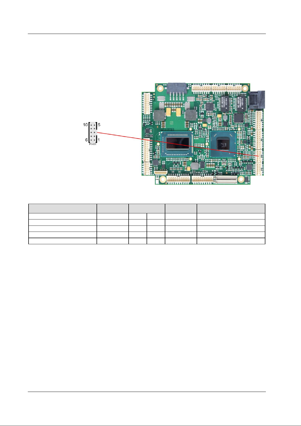
VGA Chapter: Connectors
3.8 VGA
The CRT-VGA signals are provided by a 2x5pin connector (FCI 98424-G52-10LF, mating connector e.g.
FCI 90311-010LF).
This interface allows the connection of a standard VGA-monitor. I2C communication is supported.
Description Name Pin Name Description
analog red RED 1 6 GND ground
analog green GREEN 2 7 DDDA DD data
analog blue BLUE 3 8 DDCK DD clock
vertikal sync VSYNC 4 9 GND ground
horizontal sync HSYNC 5 10 GND ground
Beckhoff New Automation Technology CB4055 page 25
Page 26
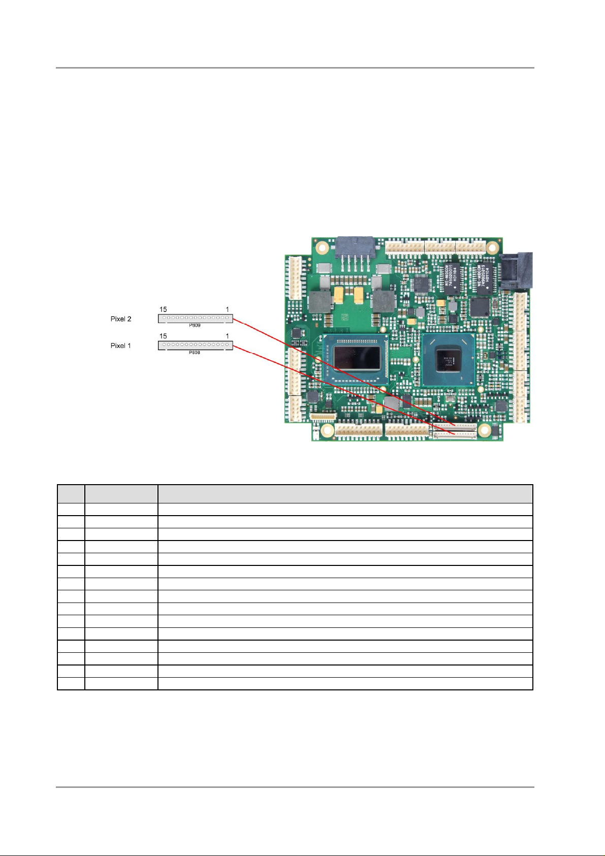
Chapter: Connectors LCD
3.9 LCD
The LCD is connected via two 15 pin connectors (Hirose DF13-15P-1.25DSA, mating connector:
DF13-15S-xxx). The power supply for the display is also provided through these connectors. The CB4055
board only supports displays with LVDS interface. For displays with digital interface an extra receiver
board is available. There is no support for DSTN displays.
With the LVDS interface it is possible to trigger LVDS displays with a maximum of 24 Bit colour depth
and one or two pixels per clock. For single pixel displays only one connector is necessary. However, if
you want to read the display's EDID data the second connector must be connected.
The display type can be chosen over the BIOS setup. Please contact your sales representative regarding
an appropriate cable to connect your display.
The following table shows the pin description for the first bit ("even" pixel).
Pin
Name Description
1 GND ground
2 GND ground
3 TXO00# LVDS even data 0 4 TXO00 LVDS even data 0 +
5 TXO01# LVDS even data 1 6 TXO01 LVDS even data 1 +
7 TXO02# LVDS even data 2 8 TXO02 LVDS even data 2 +
9 TXO0C# LVDS even clock 10 TXO0C LVDS even clock +
11 TXO03# LVDS even data 3 12 TXO03 LVDS even data 3 +
13 BL_VCC switched 5 volt for backlight
14 FP_3.3V switched 3.3 volt for display
15 FP_3.3V switched 3.3 volt for display
page 26 Beckhoff New Automation Technology CB4055
Page 27

LCD Chapter: Connectors
The following table shows the pin description for the second bit ("odd" pixel). This connector will only be
used if a display with two pixels per clockcycle is to be connected.
Pin
Name Description
1 GND ground
2 GND ground
3 TXO10# LVDS odd data 0 4 TXO10 LVDS odd data 0 +
5 TXO11# LVDS odd data 1 6 TXO11 LVDS odd data 1 +
7 TXO12# LVDS odd data 2 8 TXO12 LVDS odd data 2 +
9 TXO1C# LVDS odd clock 10 TXO1C LVDS odd clock +
11 TXO13# LVDS odd data 3 12 TXO13 LVDS odd data 3 +
13 DDC_CLK EDID clock for LCD
14 DDC_DAT EDID data for LCD
15 VCC 5 volt supply
Beckhoff New Automation Technology CB4055 page 27
Page 28

Chapter: Connectors USB
3.10 USB
USB channels 1 to 8 are provided via two 2x8pin connectors (FCI 98424-G52-16LF, mating connector
e.g. FCI 90311-016LF).
All USB-channels support USB 2.0. You may note that the setting of USB keyboard or USB mouse
support in the BIOS-setup is only necessary and advisable, if the OS offers no USB-support. BIOS-setup
can be changed with a USB keyboard without enabling USB keyboard support. Running a USB
supporting OS (such as Microsoft® Windows®) with these features enabled may lead to significant
performance or functionality limitations.
Every USB interface provides up to 500 mA current and is protected by an electronically resettable fuse.
Pinout USB 1-4:
Description Name Pin Name Description
5 volt for USB1 USB1 VCC 1 9 USB2VCC 5 volt for USB2
minus channel USB1 USB1# 2 10 USB2# minus channel USB2
plus channel USB1 USB1 3 11 USB2 plus channel USB2
ground GND 4 12 GND ground
ground GND 5 13 GND ground
plus channel USB3 USB3 6 14 USB4 plus channel USB4
minus channel USB3 USB3# 7 15 USB4# minus channel USB4
5 volt for USB3 USB3VCC 8 16 USB4VCC 5 volt for USB4
Pinout USB 5-8:
Description Name Pin Name Description
5 volt for USB5 USB5 VCC 1 9 USB6VCC 5 volt for USB6
minus channel USB5 USB5# 2 10 USB6# minus channel USB6
plus channel USB5 USB5 3 11 USB6 plus channel USB6
ground GND 4 12 GND ground
ground GND 5 13 GND ground
plus channel USB7 USB7 6 14 USB8 plus channel USB8
minus channel USB7 USB7# 7 15 USB8# minus channel USB8
5 volt for USB7 USB7VCC 8 16 USB8VCC 5 volt for USB8
page 28 Beckhoff New Automation Technology CB4055
Page 29

LAN Chapter: Connectors
3.11 LAN
Both LAN interfaces are provided via a 2x6pin connector (FCI 98424-G52-12LF, mating connector e.g.
FCI 90311-012LF). The interfaces support 10BaseT, 100BaseT, and 1000BaseT compatible network
components with automatic bandwidth selection. Additional outputs are provided for status LEDs.
Auto-negotiate and auto-cross functionality is available, PXE and RPL are available on request.
Pinout LAN interface:
Description Name Pin Name Description
LAN activity LINKACT 1 7 SPEED1000 LAN speed 1000Mbit
LAN channel 1 plus LAN1 2 8 LAN0 LAN channel 0 plus
LAN channel 1 minus LAN1# 3 9 LAN0# LAN channel 0 minus
LAN channel 3 plus LAN3 4 10 LAN2 LAN channel 2 plus
LAN channel 3 minus LAN3# 5 11 LAN2# LAN channel 2 minus
LAN speed 100Mbit SPEED100 6 12 3.3V 3.3 volt supply
Beckhoff New Automation Technology CB4055 page 29
Page 30

Chapter: Connectors Audio
3.12 Audio
The CB4055's audio functions are provided via a 2x8pin connector (FCI 98424-G52-16LF, mating
connector e.g. FCI 90311-016LF). This interface provides eight output channels for full 7.1 sound output.
Two microphone inputs and two AUX inputs are also available.
The signals "SPDIFI" and "SPDIFO" provide digital input and output. If a transformation to a coaxial or
optical connector is necessary this must be performed externally.
Description Name Pin Name Description
digital output SPDIF SPDIFO 1 9 3.3V 3.3 volt supply
digital input SPDIF SPDIFI 2 10 S_AGND analog ground sound
sound output right LOUT_R 3 11 LOUT_L sound output left
AUX input right AUXA_R 4 12 AUXA_L AUX input left
microphone input 1 MIC1 5 13 MIC2 microphone input 2
surround out right SOUT_R 6 14 SOUT_L surround out left
center output CENOUT 7 15 LFEOUT LFE output
side surround out right SSOUT_R 8 16 SSOUT_L side surround out left
page 30 Beckhoff New Automation Technology CB4055
Page 31

SATA Interfaces Chapter: Connectors
3.13 SATA Interfaces
The CB4055 provides two SATA interfaces allowing transfer rates of up to 6 Gbit per second. These
interfaces are made available via two 7 pin connectors.
The required settings are made in the BIOS setup.
Pinout SATA:
Pin
Name Description
1 GND ground
2 SATATX SATA transmit +
3 SATATX# SATA transmit 4 GND ground
5 SATARX SATA receive +
6 SATARX# SATA receive 7 GND ground
Beckhoff New Automation Technology CB4055 page 31
Page 32

Chapter: Connectors COM1 and COM2
3.14 COM1 and COM2
The serial interfaces COM1 and COM2 are provided via a 2x5pin connector (FCI 98424-G52-10LF,
mating connector e.g. FCI 90311-010LF).
Description Name Pin Name Description
data carrier detect DCD 1 6 DSR data set ready
receive data RXD 2 7 RTS request to send
transmit data TXD 3 8 CTS clear to send
data terminal ready DTR 4 9 RI ring indicator
ground GND 5 10 VCC 5 volt supply
page 32 Beckhoff New Automation Technology CB4055
Page 33

GPIO Chapter: Connectors
3.15 GPIO
The General Purpose Input/Output interface is made available through a 2x10 pin connector (FCI
98424-G52-20LF, mating connector e.g. FCI 90311-020LF). To make use of this interface the SIO unit
must be programmed accordingly. Please refer to your sales representative for information on available
software support.
Description Name Pin Name Description
ground GND 1 11 3.3V 3.3 volt supply
GP input/output 00 GPIO00 2 12 GPIO10 GP input/output 10
GP input/output 01 GPIO01 3 13 GPIO11 GP input/output 11
GP input/output 02 GPIO02 4 14 GPIO12 GP input/output 12
GP input/output 03 GPIO03 5 15 GPIO13 GP input/output 13
GP input/output 04 GPIO04 6 16 GPIO14 GP input/output 14
GP input/output 05 GPIO05 7 17 GPIO15 GP input/output 15
GP input/output 06 GPIO06 8 18 GPIO16 GP input/output 16
GP input/output 07 GPIO07 9 19 GPIO17 GP input/output 17
3.3 volt supply 3.3V 10 20 GND ground
Beckhoff New Automation Technology CB4055 page 33
Page 34

Chapter: Connectors Monitoring Functions
3.16 Monitoring Functions
Additional monitoring functions, such as the status of the fan or of other devices connected over SM-Bus
(e. g. temperature sensor), are accessible via an 10 pin connector (JST BM10B-SRSS-TB, mating
connector: SHR-10V-S(-B)).
Pin
Name Description
1 3.3V 3.3 volt supply
2 CS-SMB-CLK SMBus clock
3 CS-SMB-DAT SMBus data
4 GND ground
5 VCC 5 volt supply
6 FANCTRL1 fan 1 monitoring signal
7 FANON1 5 volt supply (switched)
8 FANCTRL2 fan 2 monitoring signal
9 FANON2 5 volt supply (switched)
10 FANCTRL3 fan 3 (external) monitoring signal
page 34 Beckhoff New Automation Technology CB4055
Page 35

HD LED Chapter: Status LEDs
4 Status LEDs
4.1 HD LED
Harddisk activity is signalled by a dedicated LED.
Beckhoff New Automation Technology CB4055 page 35
Page 36

Chapter: Status LEDs RGB LED
The microcontroller has just been flashed and is being prepared for normal
4.2 RGB LED
The CB4055 has an RGB LED, which can signal status messages by using different colors and flash
intervals.
Status Codes RGB LED:
Color Interval Meaning
none solid Invalid system state
White solid
operation after reboot
Cyan solid Reserved
Magenta solid Reserved
Blue solid Reserved
Yellow solid Reserved
Green solid Board operates normal
Red solid Board is in Reset
Green/Yellow flashing Bootloader operates normal
Red flashing Firmware is being started (start sequence still running)
Red/Yellow flashing Bootloader is being started (start sequence still running)
Red/Magenta flashing Checksum error during I2C transmission in bootloader
Red/Blue flashing Update completed, waiting for manual Reset
Yellow flashing (10s) S5 state
Yellow flashing (6s) S4 state
Yellow flashing (3s) Reserved
Yellow flashing (0.5s) Reserved
NOTE
If the board appears to be in Reset (Red LED lit) then this could also indicate a PCI104-Express "stacking
error". Such an error could occur when the stack contains a peripheral card which has the wrong type of
connector (PCI104-Express Type 1 instead of Type 2 or vice versa).
page 36 Beckhoff New Automation Technology CB4055
Page 37

Remarks for Setup Use Chapter: BIOS Settings
5 BIOS Settings
5.1 Remarks for Setup Use
In each setup page, standard values for all setup entries can be loaded. Previously saved settings are
loaded by pressing F2 and factory defaults are loaded with F3. Both F2 and F3, and also F4 ("Save &
Exit") always affect the whole set of setup entries.
Setup entries starting with a „►" sign represent submenus. Navigation between entries is done using the
arrow keys on the keyboard, with the <Enter> key being used to select an entry, which either opens up a
dialog box or opens a whole new submenu of setup entries.
Each setup entry has a short help text associated with it. This is displayed in the upper right hand corner
of the screen.
NOTE
BIOS features and setup options are subject to change without notice. The settings displayed in the
screenshots on the following pages are meant to be examples only. They do not represent the
recommended settings or the default settings. Determination of the appropriate settings is dependent
upon the particular application scenario in which the board is used.
Beckhoff New Automation Technology CB4055 page 37
Page 38

Chapter: BIOS Settings Main
5.2 Main
Aptio Setup Utility - Copyright (C) 2011 American Megatrends, Inc.
MAIN Advanced Chipset Boot Security Save & Exit
┌─────────────────────────────────────────────────────────────────┬────────────────────────────────┐
│ │Set the Date. Use Tab to │
│ Board Information │switch between Data elements. │
│ Board CB4055 │ │
│ Revision 2 │ │
│ Bios Version 1.04 │ │
│ │ │
│ Processor Information │ │
│ Name SandyBridge │ │
│ Brand String Intel(R) Core(TM) i7- │ │
│ Frequency 2100 MHz │ │
│ Processor ID 206a7 │ │
│ Stepping D2 │ │
│ Number of Processors 4Core(s) / 8Thread(s) │────────────────────────────────│
│ Microcode Revision 25 │→←: Select Screen │
│ GT Info GT2 (1200 MHz) │↑↓: Select Item │
│ │Enter: Select │
│ IGFX VBIOS Version 2124 │+/-: Change Opt. │
│ Memory RC Version 1.2.2.0 │F1: General Help │
│ Total Memory 4096 MB (DDR3) │F2: Previous Values │
│ Memory Frequency 1067 Mhz │F3: Optimized Defaults │
│ │F4: Save & Exit │
│ System Date [Tue 01/03/2012] │ESC: Exit │
│ System Time [00:47:04] │ │
│ │ │
│ │ │
│ │ │
└─────────────────────────────────────────────────────────────────┴────────────────────────────────┘
Version 2.14.1219. Copyright (C) 2011 American Megatrends, Inc.
ü Board
Options: none
ü Revision
Options: none
ü Bios Version
Options: none
ü Processor Information
Options: none
ü Name
Options: none
ü Brand String
Options: none
ü Frequency
Options: none
ü Processor ID
Options: none
ü Stepping
Options: none
ü Number of Processors
Options: none
ü Microcode Revision
Options: none
page 38 Beckhoff New Automation Technology CB4055
Page 39

Main Chapter: BIOS Settings
ü GT Info
Options: none
ü IGFX VBIOS Version
Options: none
ü Memory RC Version
Options: none
ü Total Memory
Options: none
ü Memory Frequency
Options: none
ü System Date
Options: Hier kann das Systemdatum geändert werden.
ü System Time
Options: Hier kann die Systemzeit geändert werden.
Beckhoff New Automation Technology CB4055 page 39
Page 40

Chapter: BIOS Settings Advanced
5.3 Advanced
Aptio Setup Utility - Copyright (C) 2011 American Megatrends, Inc.
Main ADVANCED Chipset Boot Security Save & Exit
┌─────────────────────────────────────────────────────────────────┬────────────────────────────────┐
│ Power-Supply Type [ATX] │Select the Type of the Power │
│► PCI Subsystem Settings │Supply: AT/ATX │
│► ACPI Settings │ │
│► CPU Configuration │ │
│► SATA Configuration │ │
│► Power Controller Options │ │
│► USB Configuration │ │
│► Super IO Configuration │ │
│► H/W Monitor │ │
│► Serial Port Console Redirection │ │
│► CPU PPM Configuration │ │
│ │ │
│ │────────────────────────────────│
│ │→←: Select Screen │
│ │↑↓: Select Item │
│ │Enter: Select │
│ │+/-: Change Opt. │
│ │F1: General Help │
│ │F2: Previous Values │
│ │F3: Optimized Defaults │
│ │F4: Save & Exit │
│ │ESC: Exit │
│ │ │
│ │ │
│ │ │
│ │ │
└─────────────────────────────────────────────────────────────────┴────────────────────────────────┘
Version 2.14.1219. Copyright (C) 2011 American Megatrends, Inc.
ü Power-Supply Type
Options: ATX / AT
ü PCI Subsystem Settings
Sub menu: see "PCI Subsystem Settings" (p. 41)
ü ACPI Settings
Sub menu: see "ACPI Settings" (p. 43)
ü CPU Configuration
Sub menu: see "CPU Configuration" (p. 44)
ü SATA Configuration
Sub menu: see "SATA Configuration" (p. 46)
ü Power Controller Options
Sub menu: see "Power Controller Options" (p. 47)
ü USB Configuration
Sub menu: see "USB Configuration" (p. 48)
ü Super IO Configuration
Sub menu: see "Super IO Configuration" (p. 49)
ü H/W Monitor
Sub menu: see "H/W Monitor" (p. 51)
ü Serial Port Console Redirection
Sub menu: see "Serial Port Console Redirection" (p. 53)
ü CPU PPM Configuration
Sub menu: see "CPU PPM Configuration" (p. 55)
page 40 Beckhoff New Automation Technology CB4055
Page 41

Advanced Chapter: BIOS Settings
5.3.1 PCI Subsystem Settings
Aptio Setup Utility - Copyright (C) 2011 American Megatrends, Inc.
Advanced
┌─────────────────────────────────────────────────────────────────┬────────────────────────────────┐
│ PCI Bus Driver Version V 2.05.02 │Enables or Disables 64bit │
│ │capable Devices to be Decoded │
│ PCI 64bit Resources Handling │in Above 4G Address Space │
│ Above 4G Deconding [Disabled] │(Only if System Supports 64 │
│ │bit PCI Decoding). │
│ PCI Common Settings │ │
│ PCI Latency Timer [32 PCI Bus Clocks] │ │
│ │ │
│► PCI Express Settings │ │
│ │ │
│ │ │
│ │ │
│ │────────────────────────────────│
│ │→←: Select Screen │
│ │↑↓: Select Item │
│ │Enter: Select │
│ │+/-: Change Opt. │
│ │F1: General Help │
│ │F2: Previous Values │
│ │F3: Optimized Defaults │
│ │F4: Save & Exit │
│ │ESC: Exit │
│ │ │
│ │ │
│ │ │
│ │ │
└─────────────────────────────────────────────────────────────────┴────────────────────────────────┘
Version 2.14.1219. Copyright (C) 2011 American Megatrends, Inc.
ü Above 4G Decoding
Options: Enabled / Disabled
ü PCI Latency Timer
Options: 32, 64,...224, 248 PCI Bus Clocks
ü PCI Express Settings
Sub menu: see "PCI Express Settings" (p. 42)
Beckhoff New Automation Technology CB4055 page 41
Page 42

Chapter: BIOS Settings Advanced
5.3.1.1 PCI Express Settings
Aptio Setup Utility - Copyright (C) 2011 American Megatrends, Inc.
Advanced
┌─────────────────────────────────────────────────────────────────┬────────────────────────────────┐
│ PCI Express Device Register Settings │Enables or Disables PCI │
│ Relaxed Ordering [Disabled] │Express Device Relaxed │
│ Extended Tag [Disabled] │Ordering │
│ No Snoop [Enabled] │ │
│ Maximum Payload [Auto] │ │
│ Maximum Read Request [Auto] │ │
│ │ │
│ PCI Express Link Register Settings │ │
│ ASPM Support [Disabled] │ │
│ WARNING: Enabling ASPM may cause some │ │
│ PCI-E devices to fail │ │
│ Extended Synch [Disabled] │ │
│ │────────────────────────────────│
│ Link Training Retry [5] │→←: Select Screen │
│ Link Training Timeout (uS) 100 │↑↓: Select Item │
│ Unpopulated Links [Disable] │Enter: Select │
│ │+/-: Change Opt. │
│ │F1: General Help │
│ │F2: Previous Values │
│ │F3: Optimized Defaults │
│ │F4: Save & Exit │
│ │ESC: Exit │
│ │ │
│ │ │
│ │ │
│ │ │
└─────────────────────────────────────────────────────────────────┴────────────────────────────────┘
Version 2.14.1219. Copyright (C) 2011 American Megatrends, Inc.
ü Relaxed Ordering
Options: Enabled / Disabled
ü Extended Tag
Options: Enabled / Disabled
ü No Snoop
Options: Enabled / Disabled
ü Maximum Payload
Options: Auto / 128 Bytes / 256 Bytes / 512 Bytes / 1024 Bytes / 2048 Bytes / 4096 Bytes
ü Maximum Read Request
Options: Auto / 128 Bytes / 256 Bytes / 512 Bytes / 1024 Bytes / 2048 Bytes / 4096 Bytes
ü ASPM Support
Options: Disabled / Auto / Force L0s
ü Extended Synch
Options: Enabled / Disabled
ü Link Training Retry
Options: Disabled / 2 / 3 / 5
ü Link Training Timeout (uS)
Options: 10...1000
ü Unpopulated Links
Options: Keep Link ON / Disable
page 42 Beckhoff New Automation Technology CB4055
Page 43

Advanced Chapter: BIOS Settings
5.3.2 ACPI Settings
Aptio Setup Utility - Copyright (C) 2011 American Megatrends, Inc.
Advanced
┌─────────────────────────────────────────────────────────────────┬────────────────────────────────┐
│ ACPI Settings │Enables or Disables BIOS ACPI │
│ │Auto Configuration. │
│ Enable ACPI Auto Configuration [Disabled] │ │
│ │ │
│ Enable Hibernation [Enabled] │ │
│ ACPI Sleep State [S1 only(CPU Stop C...] │ │
│ Lock Legacy Resources [Disabled] │ │
│ │ │
│ │ │
│ │ │
│ │ │
│ │ │
│ │────────────────────────────────│
│ │→←: Select Screen │
│ │↑↓: Select Item │
│ │Enter: Select │
│ │+/-: Change Opt. │
│ │F1: General Help │
│ │F2: Previous Values │
│ │F3: Optimized Defaults │
│ │F4: Save & Exit │
│ │ESC: Exit │
│ │ │
│ │ │
│ │ │
│ │ │
└─────────────────────────────────────────────────────────────────┴────────────────────────────────┘
Version 2.14.1219. Copyright (C) 2011 American Megatrends, Inc.
ü Enable ACPI Auto Configuration
Options: Enabled / Disabled
ü Enable Hibernation
Options: Enabled / Disabled
ü ACPI Sleep State
Options: Suspend Disabled / S1 only (CPU Stop Clock)
ü Lock Legacy Resources
Options: Enabled / Disabled
Beckhoff New Automation Technology CB4055 page 43
Page 44

Chapter: BIOS Settings Advanced
5.3.3 CPU Configuration
Aptio Setup Utility - Copyright (C) 2011 American Megatrends, Inc.
Advanced
┌─────────────────────────────────────────────────────────────────┬────────────────────────────────┐
│ CPU Configuration │Disabled for Windows XP │
│ │ │
│ Intel(R) Core(TM) i7-2710QE CPU @ 2.10GHz │ │
│ CPU Signature 206a7 │ │
│ Microcode Patch 25 │ │
│ Max CPU Speed 2100 MHz │ │
│ Min CPU Speed 800 MHz │ │
│ CPU Speed 2100 MHz │ │
│ Processor Cores 4 │ │
│ Intel HT Technology Supported │ │
│ Intel VT-x Technology Supported │ │
│ Intel SMX Technology Supported │ │
│ 64-bit Supported │ │
│ │ │
│ L1 Data Cache 32 kB x 4 │ │
│ L1 Code Cache 32 kB x 4 │────────────────────────────────│
│ L2 Cache 256 kB x 4 │→←: Select Screen │
│ L3 Cache 6144 kB │↑↓: Select Item │
│ │Enter: Select │
│ Hyper-threading [Enabled] │+/-: Change Opt. │
│ Active Processor Cores [All] │F1: General Help │
│ Limit CPUID Maximum [Disabled] │F2: Previous Values │
│ Execute Disable Bit [Enabled] │F3: Optimized Defaults │
│ Intel Virtualization Technology [Disabled] │F4: Save & Exit │
│ TCC Activation Offset 0 │ESC: Exit │
│ Primary Plane Current value 0 │ │
│ Secondary Plane Current value 0 │ │
│ │ │
└─────────────────────────────────────────────────────────────────┴────────────────────────────────┘
Version 2.14.1219. Copyright (C) 2011 American Megatrends, Inc.
ü CPU Signature
Options: none
ü Microcode Patch
Options: none
ü Max CPU Speed
Options: none
ü Min CPU Speed
Options: none
ü CPU Speed
Options: none
ü Processor Cores
Options: none
ü Intel HT Technology
Options: none
ü Intel VT-x Technology
Options: none
ü Intel SMX Technology
Options: none
ü 64-bit
Options: none
ü L1 Data Cache
Options: none
page 44 Beckhoff New Automation Technology CB4055
Page 45

Advanced Chapter: BIOS Settings
ü L1 Code Cache
Options: none
ü L2 Cache
Options: none
ü L3 Cache
Options: none
ü Hyper-threading
Options: Enabled
ü Active Processor Cores
Options: All
ü Limit CPUID Maximum
Options: Enabled / Disabled
ü Execute Disable Bit
Options: Enabled / Disabled
ü Intel Virtualization Technology
Options: Enabled / Disabled
ü TCC Activation Offset
Options: 0...50
ü Primary Plane Current value
Options: 0...255
ü Secondary Plane Current value
Options: 0...255
Beckhoff New Automation Technology CB4055 page 45
Page 46

Chapter: BIOS Settings Advanced
5.3.4 SATA Configuration
Aptio Setup Utility - Copyright (C) 2011 American Megatrends, Inc.
Advanced
┌─────────────────────────────────────────────────────────────────┬────────────────────────────────┐
│ SATA Controller(s) [Enabled] │Enable or disable SATA Device. │
│ SATA Mode Selection [RAID] │ │
│ SATA Test Mode [Disabled] │ │
│ Alternate ID [Disabled] │ │
│ │ │
│ Serial ATA Port 0 Empty │ │
│ Software Preserve Unknown │ │
│ Port 0 [Enabled] │ │
│ Hot Plug [Disabled] │ │
│ SATA Device Type [Hard Disk Drive] │ │
│ Spin Up Device [Disabled] │ │
│ Serial ATA Port 1 Empty │ │
│ Software Preserve Unknown │────────────────────────────────│
│ Port 1 [Enabled] │→←: Select Screen │
│ Hot Plug [Disabled] │↑↓: Select Item n │
│ SATA Device Type [Hard Disk Drive] │Enter: Select │
│ Spin Up Device [Disabled] │+/-: Change Opt. │
│ │F1: General Help │
│ │F2: Previous Values │
│ │F3: Optimized Defaults │
│ │F4: Save & Exit │
│ │ESC: Exit │
│ │ │
│ │ │
│ │ │
│ │ │
│ │ │
└─────────────────────────────────────────────────────────────────┴────────────────────────────────┘
Version 2.14.1219. Copyright (C) 2011 American Megatrends, Inc.
ü SATA Controller(s)
Options: Enabled / Disabled
ü SATA Mode Selection
Options: IDE / AHCI / RAID
ü SATA Test Mode
Options: Enabled / Disabled
ü Alternate ID
Options: Enabled / Disabled
ü Serial ATA Port X
Options: none
ü Software Preserve
Options: none
ü Port X
Options: Enabled / Disabled
ü Hot Plug
Options: Enabled / Disabled
ü SATA Device Type
Options: Hard Disk Drive / Solid State Drive
ü Spin Up Device
Options: Enabled / Disabled
page 46 Beckhoff New Automation Technology CB4055
Page 47

Advanced Chapter: BIOS Settings
5.3.5 Power Controller Options
Aptio Setup Utility - Copyright (C) 2011 American Megatrends, Inc.
Advanced
┌─────────────────────────────────────────────────────────────────┬────────────────────────────────┐
│ Bootloader Version 0.12-00 │Select Power line for external │
│ Firmware Version 0.17-16 │USB devices, if powered-down │
│ Mainboard Serial No 0948251130007 │ │
│ Mainboard Prod. Date (Week.Year) 47.11 │ │
│ BootCount 128 │ │
│ Minute Meter 611 │ │
│ Voltage (Min/Max) 4.60V / 5.20V │ │
│ Temperature (Min/Max) 18'C /51'C │ │
│ │ │
│ ext. USB-Port Voltage [Off in S3-5] │ │
│ int. USB-Port Voltage [Off in S3-5] │ │
│ │ │
│ WatchDogTimer Mode [Compatibility Mode] │────────────────────────────────│
│ │→←: Select Screen │
│ │↑↓: Select Item │
│ │Enter: Select │
│ │+/-: Change Opt. │
│ │F1: General Help │
│ │F2: Previous Values │
│ │F3: Optimized Defaults │
│ │F4: Save & Exit │
│ │ESC: Exit │
│ │ │
│ │ │
│ │ │
│ │ │
└─────────────────────────────────────────────────────────────────┴────────────────────────────────┘
Version 2.14.1219. Copyright (C) 2011 American Megatrends, Inc.
ü Bootloader Version
Options: none
ü Firmware Version
Options: none
ü Mainboard Serial No
Options: none
ü Mainboard Prod. Date (Week.Year)
Options: none
ü Boot Count
Options: none
ü Minute Meter
Options: none
ü Voltage (Min/Max)
Options: none
ü Temperature (Min/Max)
Options: none
ü ext. USB-Port Voltage
Options: Off in S3-5 / by SVCC
ü int. USB-Port Voltage
Options: Off in S3-5 / by SVCC
ü WatchDogTimer Mode
Options: Normal Mode / Compatibility Mode
Beckhoff New Automation Technology CB4055 page 47
Page 48

Chapter: BIOS Settings Advanced
5.3.6 USB Configuration
Aptio Setup Utility - Copyright (C) 2011 American Megatrends, Inc.
Advanced
┌─────────────────────────────────────────────────────────────────┬────────────────────────────────┐
│ USB Configuration │Enables Legacy USB support. │
│ │AUTO option disables legacy │
│ USB Devices: │support if no USB devices are │
│ 1 Keyboard, 1 Mouse, 2 Hubs │connected. DISABLE option will │
│ │keep USB devices available │
│ Legacy USB Support [Auto] │only for EFI applications. │
│ EHCI Hand-off [Disabled] │ │
│ │ │
│ USB hardware delays and time-outs: │ │
│ USB transfer time-out [5 sec] │ │
│ Device reset time-out [10 sec] │ │
│ Device power-up delay [Auto] │ │
│ │────────────────────────────────│
│ │→←: Select Screen │
│ │↑↓: Select Item │
│ │Enter: Select │
│ │+/-: Change Opt. │
│ │F1: General Help │
│ │F2: Previous Values │
│ │F3: Optimized Defaults │
│ │F4: Save & Exit │
│ │ESC: Exit │
│ │ │
│ │ │
│ │ │
│ │ │
└─────────────────────────────────────────────────────────────────┴────────────────────────────────┘
Version 2.14.1219. Copyright (C) 2011 American Megatrends, Inc.
ü USB Devices
Options: none
ü Legacy USB Support
Options: Enabled / Disabled / Auto
ü EHCI Hand-off
Options: Enabled / Disabled
ü USB transfer time-out
Options: 5 sec / 10 sec / 20 sec
ü Device reset time-out
Options: 10 sec / 20 sec / 30 sec / 40 sec
ü Device power-up delay
Options: Auto / Manual
page 48 Beckhoff New Automation Technology CB4055
Page 49

Advanced Chapter: BIOS Settings
5.3.7 Super IO Configuration
Aptio Setup Utility - Copyright (C) 2011 American Megatrends, Inc.
Advanced
┌─────────────────────────────────────────────────────────────────┬────────────────────────────────┐
│ Super IO Configuration │Set Parameters of Serial Port │
│ │0 (COMA) │
│ Super IO Chip SMSC SCH3114 │ │
│► Serial Port 0 Configuration │ │
│► Serial Port 1 Configuration │ │
│ │ │
│ │ │
│ │ │
│ │ │
│ │ │
│ │ │
│ │ │
│ │────────────────────────────────│
│ │→←: Select Screen │
│ │↑↓: Select Item │
│ │Enter: Select │
│ │+/-: Change Opt. │
│ │F1: General Help │
│ │F2: Previous Values │
│ │F3: Optimized Defaults │
│ │F4: Save & Exit │
│ │ESC: Exit │
│ │ │
│ │ │
│ │ │
│ │ │
└─────────────────────────────────────────────────────────────────┴────────────────────────────────┘
Version 2.14.1219. Copyright (C) 2011 American Megatrends, Inc.
ü Super IO Chip
Options: none
ü Serial Port X Configuration
Sub menu: see "Serial Port Configuration" (p. 50)
Beckhoff New Automation Technology CB4055 page 49
Page 50

Chapter: BIOS Settings Advanced
5.3.7.1 Serial Port Configuration
Aptio Setup Utility - Copyright (C) 2011 American Megatrends, Inc.
Advanced
┌─────────────────────────────────────────────────────────────────┬────────────────────────────────┐
│ Serial Port 0 Configuration │Enable or Disable Serial Port │
│ │(COM) │
│ Serial Port [Enabled] │ │
│ Device Settings IO=3F8h; IRQ=4; │ │
│ │ │
│ Change Settings [Auto] │ │
│ Device Mode [Normal] │ │
│ │ │
│ │ │
│ │ │
│ │ │
│ │ │
│ │────────────────────────────────│
│ │→←: Select Screen │
│ │↑↓: Select Item │
│ │Enter: Select │
│ │+/-: Change Opt. │
│ │F1: General Help │
│ │F2: Previous Values │
│ │F3: Optimized Defaults │
│ │F4: Save & Exit │
│ │ESC: Exit │
│ │ │
│ │ │
│ │ │
│ │ │
└─────────────────────────────────────────────────────────────────┴────────────────────────────────┘
Version 2.14.1219. Copyright (C) 2011 American Megatrends, Inc.
ü Serial Port
Options: Enabled / Disabled
ü Device Settings
Options: none
ü Change Settings
Options: Auto / IO=3F8h; IRQ=4 / IO=3F8h; IRQ=3, ...12 / IO=2F8h; IRQ=3, ...12 / IO=3E8h;
IRQ=3, ...12 / IO=2E8h; IRQ=3, ...12
ü Device Mode
Options: Normal / High Speed
page 50 Beckhoff New Automation Technology CB4055
Page 51

Advanced Chapter: BIOS Settings
5.3.8 H/W Monitor
Aptio Setup Utility - Copyright (C) 2011 American Megatrends, Inc.
Advanced
┌─────────────────────────────────────────────────────────────────┬────────────────────────────────┐
│ Pc Health Status │ │
│ │ │
│ CPU Temperature : +38'C │ │
│ Board Temperature : +25'C │ │
│ Memory Temperature : +40'C │ │
│ SYS FAN Speed : N/A │ │
│ CPU FAN Speed : N/A │ │
│ AUX FAN Speed : N/A │ │
│ +1.05V : +1.04 V │ │
│ VccCore : +1.07 V │ │
│ +3.3V : +3.33 V │ │
│ Vcc : +4.68 V │ │
│ +12V : +12.61 V │────────────────────────────────│
│ VTR : +3.31 V │→←: Select Screen │
│ Vbat : +0.13 V │↑↓: Select Item │
│ │Enter: Select │
│ │+/-: Change Opt. │
│ │F1: General Help │
│ │F2: Previous Values │
│ │F3: Optimized Defaults │
│ │F4: Save & Exit │
│ │ESC: Exit │
│ │ │
│ │ │
│ │ │
│ │ │
└─────────────────────────────────────────────────────────────────┴────────────────────────────────┘
Version 2.14.1219. Copyright (C) 2011 American Megatrends, Inc.
ü CPU Temperature
Options: none
ü Board Temperature
Options: none
ü Memory Temperature
Options: none
ü SYS FAN Speed
Options: none
ü CPU FAN Speed
Options: none
ü AUX FAN Speed
Options: none
ü +1.05V
Options: none
ü VccCore
Options: none
ü +3.3V
Options: none
ü Vcc
Options: none
ü +12V
Options: none
Beckhoff New Automation Technology CB4055 page 51
Page 52

Chapter: BIOS Settings Advanced
ü VTR
Options: none
ü Vbat
Options: none
page 52 Beckhoff New Automation Technology CB4055
Page 53

Advanced Chapter: BIOS Settings
5.3.9 Serial Port Console Redirection
Aptio Setup Utility - Copyright (C) 2011 American Megatrends, Inc.
Advanced
┌─────────────────────────────────────────────────────────────────┬────────────────────────────────┐
│ │Console Redirection Enable or │
│ COM0 │Disable. │
│ Console Redirection [Enabled] │ │
│► Console Redirection Settings │ │
│ │ │
│ COM1 │ │
│ Console Redirection [Disabled] │ │
│► Console Redirection Settings │ │
│ │ │
│ COM2 (Disabled) │ │
│ Console Redirection Port Is Disabled │ │
│ │ │
│ │────────────────────────────────│
│ COM3 (Disabled) │→←: Select Screen │
│ Console Redirection Port Is Disabled │↑↓: Select Item │
│ │Enter: Select │
│ │+/-: Change Opt. │
│ │F1: General Help │
│ │F2: Previous Values │
│ │F3: Optimized Defaults │
│ │F4: Save & Exit │
│ │ESC: Exit │
│ │ │
│ │ │
│ │ │
│ │ │
└─────────────────────────────────────────────────────────────────┴────────────────────────────────┘
Version 2.14.1219. Copyright (C) 2011 American Megatrends, Inc.
ü Console Redirection
Options: Enabled / Disabled
ü Console Redirection Settings
Sub menu: see "Console Redirection Settings" (p. 54)
Beckhoff New Automation Technology CB4055 page 53
Page 54

Chapter: BIOS Settings Advanced
5.3.9.1 Console Redirection Settings
Aptio Setup Utility - Copyright (C) 2011 American Megatrends, Inc.
Advanced
┌─────────────────────────────────────────────────────────────────┬────────────────────────────────┐
│ COM0 │Emulation: ANSI: Extended │
│ Console Redirection Settings │ASCII char set. VT100: ASCII │
│ │char set. VT100+: Extends │
│ Terminal Type [VT-UTF8] │VT100 to support color, │
│ Bits per second [115200] │function keys, etc. VT-UTF8: │
│ Data Bits [8] │Uses UTF8 encoding to map │
│ Parity [None] │Unicode chars onto 1 or more │
│ Stop Bits [1] │bytes. │
│ Flow Control [None] │ │
│ VT-UTF8 Combo Key Support [Enabled] │ │
│ Recorder Mode [Disabled] │ │
│ Resolution 100x31 [Enabled] │ │
│ Legacy OS Redirection Resolution [80x24] │────────────────────────────────│
│ Putty KeyPad [VT100] │→←: Select Screen │
│ │↑↓: Select Item │
│ │Enter: Select │
│ │+/-: Change Opt. │
│ │F1: General Help │
│ │F2: Previous Values │
│ │F3: Optimized Defaults │
│ │F4: Save & Exit │
│ │ESC: Exit │
│ │ │
│ │ │
│ │ │
│ │ │
└─────────────────────────────────────────────────────────────────┴────────────────────────────────┘
Version 2.14.1219. Copyright (C) 2011 American Megatrends, Inc.
ü Terminal Type
Options: VT100 / VT100+ / VT-UTF8 / ANSI
ü Bits per second
Options: 9600 / 19200 / 38400 / 57600 / 115200
ü Data Bits
Options: 7 / 8
ü Parity
Options: None / Even / Odd / Mark / Space
ü Stop Bits
Options: 1 / 2
ü Flow Control
Options: None / Hardware RTS/CTS
ü VT-UTF8 Combo Key Support
Options: Disabled / Enabled
ü Recorder Mode
Options: Disabled / Enabled
ü Resolution 100x31
Options: Disabled / Enabled
ü Legacy OS Redirection Resolution
Options: 80x24 / 80x25
ü Putty KeyPad
Options: VT100 / LINUX / XTERMR6 / SCO / ESCN / VT400
page 54 Beckhoff New Automation Technology CB4055
Page 55

Advanced Chapter: BIOS Settings
5.3.10 CPU PPM Configuration
Aptio Setup Utility - Copyright (C) 2011 American Megatrends, Inc.
Advanced
┌─────────────────────────────────────────────────────────────────┬────────────────────────────────┐
│ CPU PPM Configuration │Enable/Disable Intel SpeedStep │
│ │ │
│ EIST [Disabled] │ │
│ CPU Cx Report [C0] │ │
│ Config TDP Lock [Disabled] │ │
│ │ │
│ │ │
│ │ │
│ │ │
│ │ │
│ │ │
│ │ │
│ │────────────────────────────────│
│ │→←: Select Screen │
│ │↑↓: Select Item │
│ │Enter: Select │
│ │+/-: Change Opt. │
│ │F1: General Help │
│ │F2: Previous Values │
│ │F3: Optimized Defaults │
│ │F4: Save & Exit │
│ │ESC: Exit │
│ │ │
│ │ │
│ │ │
│ │ │
└─────────────────────────────────────────────────────────────────┴────────────────────────────────┘
Version 2.14.1219. Copyright (C) 2011 American Megatrends, Inc.
ü EIST
Options: Disabled / Enabled
ü CPU Cx Report
Options: C0 / C1 / C3 / C6 / C7
ü Config TDP LOCK
Options: Disabled / Enabled
Beckhoff New Automation Technology CB4055 page 55
Page 56

Chapter: BIOS Settings Chipset
5.4 Chipset
Aptio Setup Utility - Copyright (C) 2011 American Megatrends, Inc.
Main Advanced Chipset Boot Security Save & Exit
┌─────────────────────────────────────────────────────────────────┬────────────────────────────────┐
│► PCH-IO Configuration │System Agent (SA) Parameters │
│► System Agent (SA) Configuration │ │
│ │ │
│ │ │
│ │ │
│ │ │
│ │ │
│ │ │
│ │ │
│ │ │
│ │ │
│ │ │
│ │────────────────────────────────│
│ │→←: Select Screen │
│ │↑↓: Select Item │
│ │Enter: Select │
│ │+/-: Change Opt. │
│ │F1: General Help │
│ │F2: Previous Values │
│ │F3: Optimized Defaults │
│ │F4: Save & Exit │
│ │ESC: Exit │
│ │ │
│ │ │
│ │ │
│ │ │
└─────────────────────────────────────────────────────────────────┴────────────────────────────────┘
Version 2.14.1219. Copyright (C) 2011 American Megatrends, Inc.
ü PCH-IO Configuration
Sub menu: see "PCH-IO Configuration" (p. 57)
ü System Agent (SA) Configuration
Sub menu: see "System Agent (SA) Configuration" (p. 64)
page 56 Beckhoff New Automation Technology CB4055
Page 57

Chipset Chapter: BIOS Settings
5.4.1 PCH-IO Configuration
Aptio Setup Utility - Copyright (C) 2011 American Megatrends, Inc.
Chipset
┌─────────────────────────────────────────────────────────────────┬────────────────────────────────┐
│ Intel PCH RC Version 1.1.0.0 │Enable or disable onboard NIC. │
│ Intel PCH SKU Name QM67 │ │
│ Intel PCH Rev ID 05/B3 │ │
│ │ │
│► PCI Express Configuration │ │
│► USB Configuration │ │
│► PCH Azalia Configuration │ │
│ │ │
│ PCH LAN Controller [Enabled] │ │
│ Second LAN Controller [Enabled] │ │
│ Board Capability [SUS_PWR_DN_ACK] │ │
│ Display Logic [Enabled] │ │
│ CLKRUN# Logic [Disabled] │────────────────────────────────│
│ SB CRID [Disabled] │→←: Select Screen │
│ │↑↓: Select Item │
│ │Enter: Select │
│ High Precision Event Timer Configuration │+/-: Change Opt. │
│ High Precision Timer [Enabled] │F1: General Help │
│ │F2: Previous Values │
│ SLP_S4 Assertion Width [Disabled] │F3: Optimized Defaults │
│ Restore AC Power Loss [Power On] │F4: Save & Exit │
│ │ESC: Exit │
│ │ │
│ │ │
│ │ │
│ │ │
└─────────────────────────────────────────────────────────────────┴────────────────────────────────┘
Version 2.14.1219. Copyright (C) 2011 American Megatrends, Inc.
ü Intel PCH RC Version
Options: none
ü Intel PCH SKU Name
Options: none
ü Intel PCH Rev ID
Options: none
ü PCI Express Configuration
Sub menu: see "PCI Express Configuration" (p. 59)
ü USB Configuration
Sub menu: see "USB Configuration" (p. 62)
ü PCH Azalia Configuration
Sub menu: see "PCH Azalia Configuration" (p. 63)
ü PCH LAN Controller
Options: Disabled / Enabled
ü Second LAN Controller
Options: Disabled / Enabled
ü Board Capability
Options: SUS_PWR_DN_ACK / DeepSx
ü Display Logic
Options: Disabled / Enabled
ü CLKRUN# Logic
Options: Disabled
Beckhoff New Automation Technology CB4055 page 57
Page 58

Chapter: BIOS Settings Chipset
ü SB CRID
Options: Disabled / Enabled
ü High Precision Timer
Options: Disabled / Enabled
ü SLP_S4 Assertion Width
Options: Disabled / 1-2 Seconds / 2-3 Seconds / 3-4 Seconds / 4-5 Seconds
ü Restore AC Power Loss
Options: Power Off / Power On / Last State
page 58 Beckhoff New Automation Technology CB4055
Page 59

Chipset Chapter: BIOS Settings
5.4.1.1 PCI Express Configuration
Aptio Setup Utility - Copyright (C) 2011 American Megatrends, Inc.
Chipset
┌─────────────────────────────────────────────────────────────────┬────────────────────────────────┐
│ PCI Express Configuration │Enable or disable PCI Express │
│ │Clock Gating for each root │
│ PCI Express Clock Gating [Enabled] │port. │
│ DMI Link ASPM Control [Enabled] │ │
│ DMI Link Extended Synch Control [Disabled] │ │
│ PCIe-USB Glitch W/A [Disabled] │ │
│ Subtractive Decode [Disabled] │ │
│ │ │
│► PCI Express Root Port 1 │ │
│► PCI Express Root Port 2 │ │
│► PCI Express Root Port 3 │ │
│► PCI Express Root Port 4 │ │
│ PCIE Port 5 is assigned to LAN │────────────────────────────────│
│ PCIE Port 6 is assigned to LAN2 │→←: Select Screen │
│ │↑↓: Select Item │
│ │Enter: Select │
│ │+/-: Change Opt. │
│ │F1: General Help │
│ │F2: Previous Values │
│ │F3: Optimized Defaults │
│ │F4: Save & Exit │
│ │ESC: Exit │
│ │ │
│ │ │
│ │ │
│ │ │
└─────────────────────────────────────────────────────────────────┴────────────────────────────────┘
Version 2.14.1219. Copyright (C) 2011 American Megatrends, Inc.
ü PCI Express Clock Gating
Options: Disabled / Enabled
ü DMI Link ASPM Control
Options: Disabled / Enabled
ü DMI Link Extended Synch Control
Options: Disabled / Enabled
ü PCIe-USB Glitch W/A
Options: Disabled / Enabled
ü Subtractive Decode
Options: Disabled
ü PCI Express Root Port X
Sub menu: see "PCI Express Root Port" (p. 60)
Beckhoff New Automation Technology CB4055 page 59
Page 60

Chapter: BIOS Settings Chipset
5.4.1.1.1 PCI Express Root Port
Aptio Setup Utility - Copyright (C) 2011 American Megatrends, Inc.
Chipset
┌─────────────────────────────────────────────────────────────────┬────────────────────────────────┐
│ PCI Express Root Port 2 [Enabled] │Control the PCI Express Root │
│ ASPM Support [Auto] │Port. │
│ URR [Disabled] │ │
│ FER [Disabled] │ │
│ NFER [Disabled] │ │
│ CER [Disabled] │ │
│ CTO [Disabled] │ │
│ SEFE [Disabled] │ │
│ SENFE [Disabled] │ │
│ SECE [Disabled] │ │
│ PME SCI [Enabled] │ │
│ Hot Plug [Disabled] │ │
│ PCIe Speed [Auto] │────────────────────────────────│
│ Extra Bus Reserved 0 │→←: Select Screen │
│ Reserved Memory 10 │↑↓: Select Item │
│ Prefetchable Memory 10 │Enter: Select │
│ Reserved I/O 4 │+/-: Change Opt. │
│ │F1: General Help │
│ │F2: Previous Values │
│ │F3: Optimized Defaults │
│ │F4: Save & Exit │
│ │ESC: Exit │
│ │ │
│ │ │
│ │ │
│ │ │
└─────────────────────────────────────────────────────────────────┴────────────────────────────────┘
Version 2.14.1219. Copyright (C) 2011 American Megatrends, Inc.
ü PCI Express Root Port x
Options: Disabled / Enabled
ü ASPM Support
Options: Disabled / L0s / L1 / L0sL1 / Auto
ü URR
Options: Disabled / Enabled
ü FER
Options: Disabled / Enabled
ü NFER
Options: Disabled / Enabled
ü CER
Options: Disabled / Enabled
ü CTO
Options: Disabled / Enabled
ü SEFE
Options: Disabled / Enabled
ü SENFE
Options: Disabled / Enabled
ü SECE
Options: Disabled / Enabled
ü PME SCI
Options: Disabled / Enabled
page 60 Beckhoff New Automation Technology CB4055
Page 61

Chipset Chapter: BIOS Settings
ü Hot Plug
Options: Disabled / Enabled
ü PCIe Speed
Options: Auto / Gen1 / Gen2
ü Extra Bus Reserved
Options: 0...7
ü Reserved Memory
Options: 1...20
ü Prefetchable Memory
Options: 1...20
ü Reserved I/O
Options: 4 / 8 / 12 / 16 / 20
Beckhoff New Automation Technology CB4055 page 61
Page 62

Chapter: BIOS Settings Chipset
5.4.1.2 USB Configuration
Aptio Setup Utility - Copyright (C) 2011 American Megatrends, Inc.
Chipset
┌─────────────────────────────────────────────────────────────────┬────────────────────────────────┐
│ USB Configuration │Control the USB EHCI (USB 2.0) │
│ │functions. │
│ EHCI1 [Enabled] │One EHCI controller must │
│ EHCI2 [Enabled] │always be enabled. │
│ │ │
│ USB Ports Per-Port Disable Control [Disabled] │ │
│ │ │
│ │ │
│ │ │
│ │ │
│ │ │
│ │ │
│ │────────────────────────────────│
│ │→←: Select Screen │
│ │↑↓: Select Item │
│ │Enter: Select │
│ │+/-: Change Opt. │
│ │F1: General Help │
│ │F2: Previous Values │
│ │F3: Optimized Defaults │
│ │F4: Save & Exit │
│ │ESC: Exit │
│ │ │
│ │ │
│ │ │
│ │ │
└─────────────────────────────────────────────────────────────────┴────────────────────────────────┘
Version 2.14.1219. Copyright (C) 2011 American Megatrends, Inc.
ü EHCI1
Options: Disabled / Enabled
ü EHCI2
Options: Disabled / Enabled
ü USB Ports Per-Port Disable Control
Options: Disabled / Enabled
page 62 Beckhoff New Automation Technology CB4055
Page 63

Chipset Chapter: BIOS Settings
5.4.1.3 PCH Azalia Configuration
Aptio Setup Utility - Copyright (C) 2011 American Megatrends, Inc.
Chipset
┌─────────────────────────────────────────────────────────────────┬────────────────────────────────┐
│ PCH Azalia Configuration │Control Detection of the │
│ │Azalia device. │
│ Azalia [Auto] │Disabled = Azalia will be │
│ Azalia PME [Disabled] │unconditionally disabled │
│ Azalia Internal HDMI Codec [Disabled] │Enabled = Azalia will be │
│ │unconditionally Enabled │
│ │Auto = Azalia will be enabled │
│ │if present, disabled otherwise. │
│ │ │
│ │ │
│ │ │
│ │ │
│ │────────────────────────────────│
│ │→←: Select Screen │
│ │↑↓: Select Item │
│ │Enter: Select │
│ │+/-: Change Opt. │
│ │F1: General Help │
│ │F2: Previous Values │
│ │F3: Optimized Defaults │
│ │F4: Save & Exit │
│ │ESC: Exit │
│ │ │
│ │ │
│ │ │
│ │ │
└─────────────────────────────────────────────────────────────────┴────────────────────────────────┘
Version 2.14.1219. Copyright (C) 2011 American Megatrends, Inc.
ü Azalia
Options: Disabled / Enabled / Auto
ü Azalia PME
Options: Disabled / Enabled
ü Azalia Internal HDMI Codec
Options: Disabled / Enabled
Beckhoff New Automation Technology CB4055 page 63
Page 64

Chapter: BIOS Settings Chipset
5.4.2 System Agent (SA) Configuration
Aptio Setup Utility - Copyright (C) 2011 American Megatrends, Inc.
Chipset
┌─────────────────────────────────────────────────────────────────┬────────────────────────────────┐
│ System Agent Bridge Name SandyBridge │Check to enable VT-d function │
│ System Agent RC Version 1.1.0.0 │on MCH. │
│ │ │
│ VT-d [Disabled] │ │
│ CHAP Device (B0:D7:F0) [Disabled] │ │
│ Thermal Device (B0:D4:F0) [Disabled] │ │
│ Enable NB CRID [Disabled] │ │
│ BDAT ACPI Table Support [Disabled] │ │
│ │ │
│► Graphics Configuration │ │
│► NB PCIe Configuration │ │
│ │ │
│ │────────────────────────────────│
│ │→←: Select Screen │
│ │↑↓: Select Item │
│ │Enter: Select │
│ │+/-: Change Opt. │
│ │F1: General Help │
│ │F2: Previous Values │
│ │F3: Optimized Defaults │
│ │F4: Save & Exit │
│ │ESC: Exit │
│ │ │
│ │ │
│ │ │
│ │ │
└─────────────────────────────────────────────────────────────────┴────────────────────────────────┘
Version 2.14.1219. Copyright (C) 2011 American Megatrends, Inc.
ü VT-d
Options: Disabled / Enabled
ü CHAP Device (B0:D7:F0)
Options: Disabled / Enabled
ü Thermal Device (B0:D4:F0)
Options: Disabled / Enabled
ü Enable NB CRID
Options: Disabled / Enabled
ü BDAT ACPI Table Support
Options: Disabled / Enabled
ü Graphics Configuration
Sub menu: see "Graphics Configuration" (p. 65)
ü NB PCIe Configuration
Sub menu: see "NB PCIe Configuration" (p. 67)
page 64 Beckhoff New Automation Technology CB4055
Page 65

Chipset Chapter: BIOS Settings
5.4.2.1 Graphics Configuration
Aptio Setup Utility - Copyright (C) 2011 American Megatrends, Inc.
Chipset
┌─────────────────────────────────────────────────────────────────┬────────────────────────────────┐
│ Graphics Configuration │Graphics turbo IMON current │
│ IGFX VBIOS Version 2124 │values supported (14-31) │
│ IGfx Frequency 650 MHz │ │
│ Graphics Turbo IMON Current 31 │ │
│ │ │
│ Primary Display [Auto] │ │
│ Internal Graphics [Auto] │ │
│ GTT Size [2MB] │ │
│ Aperture Size [256MB] │ │
│ DVMT Pre-Allocated [64M] │ │
│ DVMT Total Gfx Mem [256M] │ │
│ Gfx Low Power Mode [Disabled] │ │
│► LCD Control │────────────────────────────────│
│ │→←: Select Screen │
│ │↑↓: Select Item │
│ │Enter: Select │
│ │+/-: Change Opt. │
│ │F1: General Help │
│ │F2: Previous Values │
│ │F3: Optimized Defaults │
│ │F4: Save & Exit │
│ │ESC: Exit │
│ │ │
│ │ │
│ │ │
│ │ │
└─────────────────────────────────────────────────────────────────┴────────────────────────────────┘
Version 2.14.1219. Copyright (C) 2011 American Megatrends, Inc.
ü IGFX VBIOS Version
Options: none
ü IGFX Frequency
Options: none
ü Graphics Turbo IMON Current
Options: 14...31
ü Primary Display
Options: Auto / IGFX / PEG / PCI
ü Internal Graphics
Options: Auto / Disabled / Enabled
ü GTT Size
Options: 1MB / 2MB
ü Aperture Size
Options: 128MB / 256MB / 512MB
ü DVMT Pre-Allocated
Options: 32M / 64M ... 480M / 512M / 1024M
ü DVMT Total Gfx Mem
Options: 128M / 256M / MAX
ü Gfx Low Power Mode
Options: Disabled / Enabled
ü LCD Control
Sub menu: see "LCD Control" (p. 66)
Beckhoff New Automation Technology CB4055 page 65
Page 66

Chapter: BIOS Settings Chipset
5.4.2.1.1 LCD Control
Aptio Setup Utility - Copyright (C) 2011 American Megatrends, Inc.
Chipset
┌─────────────────────────────────────────────────────────────────┬────────────────────────────────┐
│ LCD Control │Select the Video Device which │
│ │will be activated during POST. │
│ Primary IGFX Boot Display [VBIOS Default] │This has no effect if external │
│ LCD Panel Type [VBIOS Default] │graphics present. │
│ Panel Scaling [Auto] │Secondary boot display │
│ Backlight Control [PWM Inverted] │selection will appear based on │
│ BIA [Auto] │your selection. │
│ Spread Spectrum clock Chip [Off] │VGA modes will be supported │
│ ALS Support [Disabled] │only on primary display │
│ Active LFP [Int-LVDS] │ │
│ Panel Color Depth [18 Bit] │ │
│ │ │
│ │────────────────────────────────│
│ │→←: Select Screen │
│ │↑↓: Select Item │
│ │Enter: Select │
│ │+/-: Change Opt. │
│ │F1: General Help │
│ │F2: Previous Values │
│ │F3: Optimized Defaults │
│ │F4: Save & Exit │
│ │ESC: Exit │
│ │ │
│ │ │
│ │ │
│ │ │
└─────────────────────────────────────────────────────────────────┴────────────────────────────────┘
Version 2.14.1219. Copyright (C) 2011 American Megatrends, Inc.
ü Primary IGFX Boot Display
Options: VBIOS Default / CRT / EFP / LFP / EFP2 / LFP2
ü LCD Panel Type
Options: VBIOS Default / 640x480 LVDS ...1920x1080 LVDS / 2048x1536 LVDS
ü Panel Scaling
Options: Auto / Off / Force Scaling
ü Backlight Control
Options: PWM Inverted / PWM Normal / GMBus Inverted / GMBus Normal
ü Spread Spectrum Clock Chip
Options: Off / Hardware / Software
ü ALS Support
Options: Disabled / Enabled
ü Active LFP
Options: No LVDS / Int-LVDS / SDVO LVDS / eDP Port-A / eDP Port-D
ü Panel Color Depth
Options: 18 Bit / 24 Bit
page 66 Beckhoff New Automation Technology CB4055
Page 67

Chipset Chapter: BIOS Settings
5.4.2.2 NB PCIe Configuration
Aptio Setup Utility - Copyright (C) 2011 American Megatrends, Inc.
Chipset
┌─────────────────────────────────────────────────────────────────┬────────────────────────────────┐
│ NB PCIe Configuration │Configure PEG0 B0:D1:F0 │
│ PEG0 Not Present │Gen1-Gen3 │
│ PEG0 - Gen X [Auto] │ │
│ PEG0 ASPM [Auto] │ │
│ │ │
│ Enable PEG [Auto] │ │
│ De-emphasis Control [-3.5 dB] │ │
│ PEG Sampler Calibrate [Auto] │ │
│ Swing Control [Full] │ │
│ Gen3 Equalization [Disabled] │ │
│ │ │
│ │ │
│ │────────────────────────────────│
│ │→←: Select Screen │
│ │↑↓: Select Item │
│ │Enter: Select │
│ │+/-: Change Opt. │
│ │F1: General Help │
│ │F2: Previous Values │
│ │F3: Optimized Defaults │
│ │F4: Save & Exit │
│ │ESC: Exit │
│ │ │
│ │ │
│ │ │
│ │ │
└─────────────────────────────────────────────────────────────────┴────────────────────────────────┘
Version 2.14.1219. Copyright (C) 2011 American Megatrends, Inc.
ü PEGn - Gen X
Options: Auto / Gen1 / Gen2 / Gen3
ü PEGn ASPM
Options: Disabled / Auto / ASPM L0s / ASPM L1 / ASPM L0sL1
ü Enable PEG
Options: Disabled / Enabled / Auto
ü De-emphasis Control
Options: -6 dB / -3.5 dB
ü PEG Sampler Calibrate
Options: Auto / Disabled / Enabled
ü Swing Control
Options: Reduced / Half / Full
ü Gen3 Equalization
Options: Disabled / Enabled
Beckhoff New Automation Technology CB4055 page 67
Page 68

Chapter: BIOS Settings Boot
5.5 Boot
Aptio Setup Utility - Copyright (C) 2011 American Megatrends, Inc.
Main Advanced Chipset Boot Security Save & Exit
┌─────────────────────────────────────────────────────────────────┬────────────────────────────────┐
│ Boot Configuration │Number of 1/10 sec. to wait │
│ Setup Prompt Timeout 5 │for setup activation key. 0 │
│ Bootup NumLock State [On] │means no wait. │
│ │ │
│ Full Screen Logo [Enabled] │ │
│ Fast Boot [Disabled] │ │
│ │ │
│ CSM16 Module Version 07.69 │ │
│ │ │
│ GateA20 Active [Upon Request] │ │
│ INT19 Trap Request [Postponed] │ │
│ │ │
│ Boot Option Priorities │────────────────────────────────│
│ Boot Option #1 [IBA GE Slot 00C8 v...] │→←: Select Screen │
│► CSM Parameters │↑↓: Select Item │
│ │Enter: Select │
│ │+/-: Change Opt. │
│ │F1: General Help │
│ │F2: Previous Values │
│ │F3: Optimized Defaults │
│ │F4: Save & Exit │
│ │ESC: Exit │
│ │ │
│ │ │
│ │ │
│ │ │
└─────────────────────────────────────────────────────────────────┴────────────────────────────────┘
Version 2.14.1219. Copyright (C) 2011 American Megatrends, Inc.
ü Setup Prompt Timeout
Options: 0...65535 [x 1/10 sec.]
ü Bootup NumLock State
Options: On / Off
ü Full Screen Logo
Options: Disabled / Enabled
ü Fast Boot
Options: Disabled / Enabled
ü Skip VGA
Options: Disabled / Enabled
ü Skip USB
Options: Disabled / Enabled
ü Skip PS2
Options: Disabled / Enabled
ü CSM16 Module Version
Options: none
ü GateA20 Active
Options: Upon Request / Always
ü ING19 Trap Response
Options: Immediate / Postponed
page 68 Beckhoff New Automation Technology CB4055
Page 69

Boot Chapter: BIOS Settings
ü Boot Option Priorities
Options: Review or change the sequence of available boot devices
ü CSM Parameters
Sub menu: see "CSM Parameters" (p. 70)
Beckhoff New Automation Technology CB4055 page 69
Page 70

Chapter: BIOS Settings Boot
5.5.1 CSM Parameters
Aptio Setup Utility - Copyright (C) 2011 American Megatrends, Inc.
Main Advanced Chipset BOOT Security Save & Exit
┌─────────────────────────────────────────────────────────────────┬────────────────────────────────┐
│ Boot option filter [Legacy only] │System Agent (SA) Parameters │
│ Launch PXE OpROM policy [Enable] │ │
│ │ │
│ Other PCI device ROM priority [Legacy OpROM] │ │
│ │ │
│ │ │
│ │ │
│ │ │
│ │ │
│ │ │
│ │ │
│ │ │
│ │────────────────────────────────│
│ │→←: Select Screen │
│ │↑↓: Select Item │
│ │Enter: Select │
│ │+/-: Change Opt. │
│ │F1: General Help │
│ │F2: Previous Values │
│ │F3: Optimized Defaults │
│ │F4: Save & Exit │
│ │ESC: Exit │
│ │ │
│ │ │
│ │ │
│ │ │
└─────────────────────────────────────────────────────────────────┴────────────────────────────────┘
Version 2.14.1219. Copyright (C) 2011 American Megatrends, Inc.
ü Boot option filter
Options: UEFI and Legacy / Legacy only / UEFI only
ü Launch PXE OpROM policy
Options: Disabled / Enabled
ü Other PCI device ROM priority
Options: UEFI OpROM / Legacy OpROM
page 70 Beckhoff New Automation Technology CB4055
Page 71

Security Chapter: BIOS Settings
5.6 Security
Aptio Setup Utility - Copyright (C) 2011 American Megatrends, Inc.
Main Advanced Chipset Boot Security Save & Exit
┌─────────────────────────────────────────────────────────────────┬────────────────────────────────┐
│ Password Description │Set Administrator Password │
│ │ │
│ If ONLY the Administrator's password is set, │ │
│ then this only limits access to Setup and is │ │
│ only asked for when entering Setup. │ │
│ If ONLY the User's password is set, then this │ │
│ is a power on password and must be entered to │ │
│ boot or enter Setup. In Setup the User will │ │
│ Administrator rights. │ │
│ The password length must be │ │
│ in the following range: │ │
│ Minimum length 3 │ │
│ Maximum length 20 │────────────────────────────────│
│ │→←: Select Screen │
│ │↑↓: Select Item │
│ Administrator Password │Enter: Select │
│ User Password │+/-: Change Opt. │
│ │F1: General Help │
│ │F2: Previous Values │
│ UEFI Secure Boot Management │F3: Optimized Defaults │
│ Secure Boot control [Enabled] │F4: Save & Exit │
│► Secure Boot Policy │ESC: Exit │
│► Key Management │ │
│ │ │
│ │ │
│ │ │
└─────────────────────────────────────────────────────────────────┴────────────────────────────────┘
Version 2.14.1219. Copyright (C) 2011 American Megatrends, Inc.
ü Administrator Password
Options: Press [Enter]
ü User Password
Options: Press [Enter]
ü Secure Boot control
Options: Disabled / Enabled
ü Secure Boot Policy
Sub menu: see "Secure Boot Policy" (p. 72)
ü Key Management
Sub menu: see "Key Management" (p. 73)
Beckhoff New Automation Technology CB4055 page 71
Page 72

Chapter: BIOS Settings Security
5.6.1 Secure Boot Policy
Aptio Setup Utility - Copyright (C) 2011 American Megatrends, Inc.
Security
┌─────────────────────────────────────────────────────────────────┬────────────────────────────────┐
│ Internal RV [Always Execute] │Image Execution Policy on │
│ Option ROM [Deny Execute] │Security Violation. Image load │
│ Removable Media [Deny Execute] │device path │
│ Fixed Media [Deny Execute] │ │
│ │ │
│ │ │
│ │ │
│ │ │
│ │ │
│ │ │
│ │ │
│ │ │
│ │────────────────────────────────│
│ │→←: Select Screen │
│ │↑↓: Select Item │
│ │Enter: Select │
│ │+/-: Change Opt. │
│ │F1: General Help │
│ │F2: Previous Values │
│ │F3: Optimized Defaults │
│ │F4: Save & Exit │
│ │ESC: Exit │
│ │ │
│ │ │
│ │ │
│ │ │
└─────────────────────────────────────────────────────────────────┴────────────────────────────────┘
Version 2.14.1219. Copyright (C) 2011 American Megatrends, Inc.
ü Internal FV
Options: Always Execute
ü Option ROM
Options: Always Execute / Always Deny / Allow Execute / Defer Execute / Deny Execute / Query
User
ü Removable Media
Options: Always Execute / Always Deny / Allow Execute / Defer Execute / Deny Execute / Query
User
ü Fixed Media
Options: Always Execute / Always Deny / Allow Execute / Defer Execute / Deny Execute / Query
User
page 72 Beckhoff New Automation Technology CB4055
Page 73

Security Chapter: BIOS Settings
5.6.2 Key Management
Aptio Setup Utility - Copyright (C) 2011 American Megatrends, Inc.
Security
┌─────────────────────────────────────────────────────────────────┬────────────────────────────────┐
│ System Mode Setup │Launches the Filebrowser to │
│ Secure Boot Mode Disabled │set the Platform Key from file │
│ │ │
│ Platform Key (PK) NOT INSTALLED │ │
│► Set PK from File │ │
│► Get PK to File │ │
│► Delete the PK │ │
│ Key Exchange Key Database(KEK) NOT INSTALLED │ │
│► Set KEK from File │ │
│► Get KEK to File │ │
│► Delete the KEK │ │
│► Append an entry to KEK │ │
│ Authorized Signature Database(DB) NOT INSTALLED │────────────────────────────────│
│► Set DB from File │→←: Select Screen │
│► Get DB to File │↑↓: Select Item │
│► Delete the DB │Enter: Select │
│► Append an entry to DB │+/-: Change Opt. │
│ Forbidden Signature Database(DBX) NOT INSTALLED │F1: General Help │
│► Set DBX from File │F2: Previous Values │
│► Get DBX to File │F3: Optimized Defaults │
│► Delete the DBX │F4: Save & Exit │
│► Append an entry to DBX │ESC: Exit │
│ │ │
│ Manage All Factory Keys (PK,KEK,DB,DBX) │ │
│ Install Factory Defaults │ │
│ │ │
└─────────────────────────────────────────────────────────────────┴────────────────────────────────┘
Version 2.14.1219. Copyright (C) 2011 American Megatrends, Inc.
ü System Mode
Options: none
ü Secure Boot Mode
Options: none
ü Set PK from File
Options: Press [Enter]
ü Get PK to File
Options: Press [Enter]
ü Delete the PK
Options: Press [Enter]
ü Set KEK from File
Options: Press [Enter]
ü Get KEK to File
Options: Press [Enter]
ü Delete the KEK
Options: Press [Enter]
ü Append an entry to KEK
Options: Press [Enter]
ü Set DB from File
Options: Press [Enter]
ü Get DB to File
Options: Press [Enter]
Beckhoff New Automation Technology CB4055 page 73
Page 74

Chapter: BIOS Settings Security
ü Delete the DB
Options: Press [Enter]
ü Append an entry to DB
Options: Press [Enter]
ü Set DBX from File
Options: Press [Enter]
ü Get DBX to File
Options: Press [Enter]
ü Delete the DBX
Options: Press [Enter]
ü Append an entry to DBX
Options: Press [Enter]
ü Install Factory Defaults
Options: Press [Enter]
page 74 Beckhoff New Automation Technology CB4055
Page 75

Save & Exit Chapter: BIOS Settings
5.7 Save & Exit
Aptio Setup Utility - Copyright (C) 2011 American Megatrends, Inc.
Main Advanced Chipset Boot Security Save & Exit
┌─────────────────────────────────────────────────────────────────┬────────────────────────────────┐
│ Save Changes and Reset │Reset the system after saving │
│ Discard Changes and Reset │the changes. │
│ │ │
│ Restore Defaults │ │
│ Save as User Defaults │ │
│ Restore User Defaults │ │
│ │ │
│ Boot Override │ │
│ │ │
│ │ │
│ │ │
│ │ │
│ │────────────────────────────────│
│ │→←: Select Screen │
│ │↑↓: Select Item │
│ │Enter: Select │
│ │+/-: Change Opt. │
│ │F1: General Help │
│ │F2: Previous Values │
│ │F3: Optimized Defaults │
│ │F4: Save & Exit │
│ │ESC: Exit │
│ │ │
│ │ │
│ │ │
│ │ │
└─────────────────────────────────────────────────────────────────┴────────────────────────────────┘
Version 2.14.1219. Copyright (C) 2011 American Megatrends, Inc.
ü Save Changes and Reset
Options: Press [Enter]
ü Discard Changes and Reset
Options: Press [Enter]
ü Restore Defaults
Options: Press [Enter]
ü Save as User Defaults
Options: Press [Enter]
ü Restore User Defaults
Options: Press [Enter]
ü Boot Override
Options: Press [Enter]
Beckhoff New Automation Technology CB4055 page 75
Page 76

Chapter: BIOS Settings BIOS update
5.8 BIOS update
If a BIOS update becomes necessary, the program “AFUDOS.EXE” from AMI® is used for this. It is
important, that the program is started from a DOS environment without a virtual memory manager such
as for example “EMM386.EXE”. In case such a memory manager is loaded, the program will stop with an
error message.
The system must not be interrupted during the flash process, otherwise the update is stopped and the
BIOS is destroyed afterwards.
The program should be started as follows:
afudos [romfile] /p /b /n
/p Program BIOS file
/b Program boot block
/n Program NVRAM
CAUTION
Updating the BIOS in an improper way can render the board unusable. Therefore, you should only update
the BIOS if you really need the changes/corrections which come with the new BIOS version.
CAUTION
Before you proceed to update the BIOS you need to make absolutely sure that you have the right BIOS
file which was issued for the exact board and exact board revision that you wish to update. If you try to
update the BIOS using the wrong file the board will not start up again.
page 76 Beckhoff New Automation Technology CB4055
Page 77

PCB: Mounting Holes Chapter: Mechanical Drawing
6 Mechanical Drawing
6.1 PCB: Mounting Holes
A true dimensioned drawing can be found in the PC/104 specification.
NOTE
All dimensions are in mil (1 mil = 0,0254 mm)
Beckhoff New Automation Technology CB4055 page 77
Page 78

Chapter: Mechanical Drawing PCB: Pin 1 Dimensions
6.2 PCB: Pin 1 Dimensions
NOTE
All dimensions are in mil (1 mil = 0,0254 mm)
page 78 Beckhoff New Automation Technology CB4055
Page 79

PCB: Heat Sink/Die Center Chapter: Mechanical Drawing
6.3 PCB: Heat Sink/Die Center
NOTE
All dimensions are in mil (1 mil = 0,0254 mm)
Beckhoff New Automation Technology CB4055 page 79
Page 80

Chapter: Technical Data Electrical Data
7 Technical Data
7.1 Electrical Data
Power Supply:
Board: 5 Volt and 12 Volt (+/- 5%)
RTC: >= 3 Volt
Electric Power Consumption:
Board: tbd
RTC: <= 10µA
7.2 Environmental Conditions
Temperature Range:
Operating: 0°C to +60°C (extended temperature on request)
Storage: -25°C up to +85°C
Shipping: -25°C up to +85°C, for packaged boards
Temperature Changes:
Operating: 0.5°C per minute, 7.5°C per 30 minutes
Storage: 1.0°C per minute
Shipping: 1.0°C per minute, for packaged boards
Relative Humidity:
Operating: 5% up to 85% (non condensing)
Storage: 5% up to 95% (non condensing)
Shipping: 5% up to 100% (non condensing), for packaged boards
Shock:
Operating: 150m/s2, 6ms
Storage: 400m/s2, 6ms
Shipping: 400m/s2, 6ms, for packaged boards
Vibration:
Operating: 10 up to 58Hz, 0.075mm amplitude
58 up to 500Hz, 10m/s2
Storage: 5 up to 9Hz, 3.5mm amplitude
9 up to 500Hz, 10m/s2
Shipping: 5 up to 9Hz, 3.5mm amplitude
9 up to 500Hz, 10m/s2, for packaged boards
CAUTION
Shock and vibration figures pertain to the motherboard alone and do not include additional components
such as heat sinks, memory modules, cables etc.
page 80 Beckhoff New Automation Technology CB4055
Page 81

Thermal Specifications Chapter: Technical Data
7.3 Thermal Specifications
The board is specified to operate in an environmental temperature range from 0°C to +60°C (extended
temperature on request). Maximum die temperature is 100°C. To keep the processor under this threshold
an appropriate cooling solution needs to be applied. This solution has to take typical and maximum power
consumption into account. The maximum power consumption may be twice as high and should be used
as a basis for the cooling concept. Additional controllers may also affect the cooling concept. The power
consumption of such components may be comparable to the consumption of the processor.
The board design includes thermal solution mounting points that will provide the best possible thermal
interface between die and solution. Since we take thermal solutions seriously we have several advanced,
aggressive cooling solutions in our product portfolio. Please contact your sales representative to order or
discuss your thermal solution needs.
CAUTION
The end customer has the responsibility to ensure that the die temperature of the processor does not
exceed 100°C. Permanent overheating may destroy the board!
In case the temperature exceeds 100°C the environmental temperature must be reduced. Under certain
circumstances sufficient air circulation must be provided.
CAUTION
The CB4055 includes circuitry that will notify an intelligent power supply to shut down if the processor
reaches a critical temperature. This is achieved by deasserting the (low-active) PS_ON# signal found on
the SM-Bus connector. When PS_ON# is no longer pulled low, an intelligent power supply would take this
as a signal to shut down power. For this to work, PS_ON# must be connected to the power supply's
PS_ON input. If PS_ON# is not otherwise connected, the CB4055 can be damaged beyond repair if a
thermal shutdown event occurs. In rare instances, if power is not shut down, the board will continue to
heat up until failure occurs.
Beckhoff New Automation Technology CB4055 page 81
Page 82

Chapter: Support and Service Beckhoff's Branch Offices and Representatives
8 Support and Service
Beckhoff and their partners around the world offer comprehensive support and service, making available
fast and competent assistance with all questions related to Beckhoff products and system solutions.
8.1 Beckhoff's Branch Offices and Representatives
Please contact your Beckhoff branch office or representative for local support and service on Beckhoff
products.
The addresses of Beckhoff's branch offices and representatives around the world can be found on her
internet pages: http://www.beckhoff.com
You will also find further documentation for Beckhoff components there.
8.2 Beckhoff Headquarters
Beckhoff Automation GmbH
Eiserstr. 5
33415 Verl
Germany
phone: +49(0)5246/963-0
fax: +49(0)5246/963-198
e-mail: info@beckhoff.com
web: www.beckhoff.com
8.2.1 Beckhoff Support
Support offers you comprehensive technical assistance, helping you not only with the application of
individual Beckhoff products, but also with other, wide-ranging services:
o support
o design, programming and commissioning of complex automation systems
o and extensive training programs for Beckhoff system components
hotline: +49(0)5246/963-157
fax: +49(0)5246/963-9157
e-mail: support@beckhoff.com
8.2.2 Beckhoff Service
The Beckhoff Service Center supports you in all matters of after-sales service:
o on-site service
o repair service
o spare parts service
o hotline service
hotline: +49(0)5246/963-460
fax: +49(0)5246/963-479
e-mail: service@beckhoff.com
page 82 Beckhoff New Automation Technology CB4055
Page 83

Anhang: Post-Codes
I Anhang: Post-Codes
During boot, the BIOS generates a sequence of status codes (so-called "POST codes"), which can be
viewed using a special output device (POST code card). The meaning of these codes is described in the
document "Aptio™ 4.x Status Codes" by American Megatrends®, which can be downloaded from their
website http://www.ami.com. The following additional OEM POST codes are generated:
Code Description
87h BIOS-API started
88h PCA9535 started
89h PWRCTRL-Firmware started
Beckhoff New Automation Technology CB4055 page 83
Page 84

Annex: Resources
II Annex: Resources
IO Range
The used resources depend on setup settings.
The given values are ranges, which are fixed by AT compatibility. Other IO ranges are used, which are
dynamically adjusted by Plug & Play BIOS while booting.
Address Function
0-FF Reserved IO area of the board
170-17F
1F0-1F7
278-27F
2E8-2EF
2F8-2FF COM2
370-377
378-37F
3BC-3BF
3E8-3EF
3F0-3F7
3F8-3FF COM1
Memory Range
The used resources depend on setup settings.
If the entire range is clogged through option ROMs, these functions do not work anymore.
Address Function
A0000-BFFFF VGA RAM
C0000-CFFFF VGA BIOS
D0000-E7FFF AHCI BIOS / RAID / PXE (if available)
E8000-FFFFF System BIOS
Interrupt
The used resources depend on setup settings.
The listed interrupts and their use are given through AT compatibility.
If interrupts must exclusively be available on the ISA side, they have to be reserved through the BIOS
setup. The exclusivity is not given and not possible on the PCI side.
Address Function
IRQ0 Timer
IRQ1 PS/2 Keyboard
IRQ2 (9)
IRQ3 COM1
IRQ4 COM2
IRQ5
IRQ6
IRQ7
IRQ8 RTC
IRQ9
IRQ10
IRQ11
IRQ12 PS/2 Mouse
page 84 Beckhoff New Automation Technology CB4055
Page 85

Annex: Resources
Address Function
IRQ13 FPU
IRQ14
IRQ15
PCI Devices
All listed PCI devices exist on the board. Some PCI devices or functions of devices may be disabled in
the BIOS setup. Once a device is disabled other devices may get PCI bus numbers different from the
ones listed in the table.
AD INTA REQ Bus Dev. Fct. Controller / Slot
- - 0 0 0 Host Bridge ID0104h
A - 0 2 0 VGA Graphics ID0106h
A - 0 25 0 LAN QM67 ID1502h
A - 0 26 0 USB EHCI Controller #2 QM67 ID1C2Dh
A - 0 27 0 HDA Controller QM67 ID1C20h
A - 0 28 0 PCI Express Port 1 QM67 ID1C10h
B - 0 28 1 [PCI Express Port 2 QM67 ID1C12h]
C - 0 28 2 [PCI Express Port 3 QM67 ID1C14h]
D - 0 28 3 [PCI Express Port 4 QM67 ID1C16h]
A - 0 28 4 PCI Express Port 5 QM67 ID1C18h
B - 0 28 5 PCI Express Port 6 QM67 ID1C1Ah
A - 0 29 0 USB EHCI Controller #1 QM76 ID1C26h
- - 0 31 0 ISA Bridge QM67 ID1C4Fh
B - 0 31 2 SATA Interface QM67 ID1C03h
B - 0 31 3 SMBus Interface QM67 ID1C22h
A - m 0 0 LAN 82547L ID10D3h
SMB Devices
The following table contains all reserved SM-Bus device addresses in 8-bit notation. Note that external
devices must not use any of these addresses even if the component mentioned in the table is not present
on the motherboard.
Address Function
10-11 Standard slave address
40-41 GPIO
60-61 BIOS internal
70-73 POST code output
88-89 BIOS-defined slave address
A0-A1 DIMM 1
A2-A3 DIMM 2
A4-AF BIOS internal
B0-BF BIOS internal
D2-D3 Clock
Beckhoff New Automation Technology CB4055 page 85
 Loading...