

Page 1
CB4053
Manual
rev. 1.6
Beckhoff Automation GmbH phone: +49 (0) 52 46/963-0
Eiserstr. 5 fax: +49 (0) 52 46/963-198
33415 Verl email: info@beckhoff.de
Germany web: www.beckhoff.de
Page 2

Page 3

Contents
Contents
0 Document History ................................................................................................................................. 5
1 Introduction ........................................................................................................................................... 6
1.1 Notes on the Documentation ......................................................................................................... 6
1.1.1 Liability Conditions ................................................................................................................ 6
1.1.2 Copyright ............................................................................................................................... 6
1.2 Safety Instructions ......................................................................................................................... 7
1.2.1 Disclaimer .............................................................................................................................. 7
1.2.2 Description of Safety Symbols .............................................................................................. 7
1.3 Essential Safety Measures ............................................................................................................ 8
1.3.1 Operator's Obligation to Exercise Diligence .......................................................................... 8
1.3.2 National Regulations Depending on the Machine Type ........................................................ 8
1.3.3 Operator Requirements ......................................................................................................... 8
1.4 Functional Range .......................................................................................................................... 9
2 Overview ............................................................................................................................................. 10
2.1 Features ...................................................................................................................................... 10
2.2 Specifications and Documents .................................................................................................... 12
3 Detailed Description ........................................................................................................................... 13
3.1 Power Supply .............................................................................................................................. 13
3.2 CPU ............................................................................................................................................. 13
3.3 Memory ....................................................................................................................................... 13
4 Connectors ......................................................................................................................................... 14
4.1 Connector Map ............................................................................................................................ 15
4.2 Power Supply .............................................................................................................................. 16
4.3 System ........................................................................................................................................ 17
4.4 Memory ....................................................................................................................................... 18
4.5 PC/104-Bus ................................................................................................................................. 21
4.6 PC/104-Plus Bus ......................................................................................................................... 23
4.7 VGA ............................................................................................................................................. 25
4.8 LCD ............................................................................................................................................. 26
4.9 USB ............................................................................................................................................. 28
4.10 LAN.............................................................................................................................................. 30
4.11 Audio ........................................................................................................................................... 31
4.12 IDE Interface ............................................................................................................................... 32
4.13 Parallel Interface LPT .................................................................................................................. 34
4.14 Serial Interface COM1 ................................................................................................................. 35
4.15 Serial Interface COM2 ................................................................................................................. 36
4.16 SMBus ......................................................................................................................................... 37
4.17 Monitoring Functions ................................................................................................................... 38
4.18 Fan .............................................................................................................................................. 39
5 Status LEDs ........................................................................................................................................ 40
5.1 HD LED ....................................................................................................................................... 40
5.2 RGB LED ..................................................................................................................................... 41
6 BIOS Settings ..................................................................................................................................... 42
6.1 Remarks for Setup Use ............................................................................................................... 42
6.2 Top Level Menu ........................................................................................................................... 42
6.3 Standard CMOS Features ........................................................................................................... 43
Beckhoff New Automation Technology CB4053 page 3
Page 4

Contents
6.3.1 IDE Channel 0 Master/Slave ............................................................................................... 44
6.4 Advanced BIOS Features ........................................................................................................... 45
6.4.1 CPU Feature ....................................................................................................................... 47
6.4.2 Hard Disk Boot Priority ........................................................................................................ 48
6.5 Advanced Chipset Features ........................................................................................................ 49
6.6 Integrated Peripherals ................................................................................................................. 50
6.6.1 OnChip IDE Devices ........................................................................................................... 52
6.6.2 Onboard Devices ................................................................................................................. 53
6.6.3 PCI Express Root Port Function ......................................................................................... 54
6.6.4 USB Device Setting ............................................................................................................. 55
6.7 Power Management Setup .......................................................................................................... 56
6.7.1 HPET Feature ..................................................................................................................... 57
6.7.2 Intel DTS Feature ................................................................................................................ 58
6.8 PnP/PCI Configuration ................................................................................................................ 59
6.8.1 IRQ Resources .................................................................................................................... 60
6.9 PC Health Status ......................................................................................................................... 61
6.10 Load Fail-Safe Defaults ............................................................................................................... 63
6.11 Load Optimized Defaults ............................................................................................................. 63
6.12 Set Password .............................................................................................................................. 63
6.13 Save & Exit Setup ....................................................................................................................... 63
6.14 Exit Without Saving ..................................................................................................................... 63
7 BIOS update ....................................................................................................................................... 64
8 Mechanical Drawing ........................................................................................................................... 65
8.1 PCB: Mounting Holes .................................................................................................................. 65
8.2 PCB: Pin 1 Dimensions ............................................................................................................... 66
8.3 PCB: Heat Sink ........................................................................................................................... 67
9 Technical Data .................................................................................................................................... 68
9.1 Electrical Data ............................................................................................................................. 68
9.2 Environmental Conditions ........................................................................................................... 68
9.3 Thermal Specifications ................................................................................................................ 69
10 Support and Service ........................................................................................................................... 70
10.1 Beckhoff's Branch Offices and Representatives ......................................................................... 70
10.2 Beckhoff Headquarters................................................................................................................ 70
10.2.1 Beckhoff Support ................................................................................................................. 70
10.2.2 Beckhoff Service ................................................................................................................. 70
I Annex: Post-Codes ............................................................................................................................. 71
II Annex: Resources .............................................................................................................................. 74
A IO Range ......................................................................................................................................... 74
B Memory Range ................................................................................................................................ 74
C Interrupt ........................................................................................................................................... 74
D PCI Devices ..................................................................................................................................... 75
E SMB Devices ................................................................................................................................... 75
page 4 Beckhoff New Automation Technology CB4053
Page 5
Notes on the Documentation Chapter: Document History
0 Document History
Version Changes
0.1 first pre-release
0.9 first complete version, todo: update photographs to G2
1.0 added SSD description, updated thermal specs, minor corrections
1.1 new photographs, updated contact details, minor changes
1.2 added pinout for RS-422/RS-485 COM soldering option, minor changes
1.3 minor changes
1.4 updated block diagram (ALC 885 EOL, 8GB SSD),
added "3.3V only" warning for IDE, added note concerning PS_ON,
minor changes
1.5 added description of status LEDs, added labels to LVDS connector symbols, minor
changes
1.6 new cover picture; improved output quality of dimensional drawings
NOTE
All company names, brand names, and product names referred to in this manual are registered or
unregistered trademarks of their respective holders and are, as such, protected by national and
international law.
Beckhoff New Automation Technology CB4053 page 5
Page 6

Chapter: Introduction Notes on the Documentation
1 Introduction
1.1 Notes on the Documentation
This description is only intended for the use of trained specialists in control and automation engineering
who are familiar with the applicable national standards. It is essential that the following notes and
explanations are followed when installing and commissioning these components.
1.1.1 Liability Conditions
The responsible staff must ensure that the application or use of the products described satisfy all the
requirements for safety, including all the relevant laws, regulations, guidelines and standards.
The documentation has been prepared with care. The products described are, however, constantly under
development. For that reason the documentation is not in every case checked for consistency with
performance data, standards or other characteristics. None of the statements of this manual represents a
guarantee (Garantie) in the meaning of § 443 BGB of the German Civil Code or a statement about the
contractually expected fitness for a particular purpose in the meaning of § 434 par. 1 sentence 1 BGB. In
the event that it contains technical or editorial errors, we retain the right to make alterations at any time
and without warning. No claims for the modification of products that have already been supplied may be
made on the basis of the data, diagrams and descriptions in this documentation.
1.1.2 Copyright
© This documentation is copyrighted. Any reproduction or third party use of this publication, whether in
whole or in part, without the written permission of Beckhoff Automation GmbH, is forbidden.
page 6 Beckhoff New Automation Technology CB4053
Page 7
Safety Instructions Chapter: Introduction
1.2 Safety Instructions
Please consider the following safety instructions and descriptions. Product specific safety instructions are
to be found on the following pages or in the areas mounting, wiring, commissioning etc.
1.2.1 Disclaimer
All the components are supplied in particular hardware and software configurations appropriate for the
application. Modifications to hardware or software configurations other than those described in the
documentation are not permitted, and nullify the liability of Beckhoff Automation GmbH.
1.2.2 Description of Safety Symbols
The following safety symbols are used in this documentation. They are intended to alert the reader to the
associated safety instructions.
ACUTE RISK OF INJURY!
If you do not adhere to the safety advise next to this symbol, there is immediate danger to life and health
of individuals!
RISK OF INJURY!
If you do not adhere to the safety advise next to this symbol, there is danger to life and health of
individuals!
HAZARD TO INDIVIDUALS, ENVIRONMENT, DEVICES, OR DATA!
If you do not adhere to the safety advise next to this symbol, there is obvious hazard to individuals, to
environment, to materials, or to data.
NOTE OR POINTER
This symbol indicates information that contributes to better understanding.
Beckhoff New Automation Technology CB4053 page 7
Page 8

Chapter: Introduction Essential Safety Measures
1.3 Essential Safety Measures
1.3.1 Operator's Obligation to Exercise Diligence
The operator must ensure that
o the product is only used for its intended purpose
o the product is only operated in sound condition and in working order
o the instruction manual is in good condition and complete, and always available for reference at the
location where the products are used
o the product is only used by suitably qualified and authorised personnel
o the personnel is instructed regularly about relevant occupational safety and environmental protection
aspects
o the operating personnel is familiar with the operating manual and in particular the safety notes
contained herein
1.3.2 National Regulations Depending on the Machine Type
Depending on the type of machine and plant in which the product is used, national regulations governing
the controllers of such machines will apply, and must be observed by the operator. These regulations
cover, amongst other things, the intervals between inspections of the controller. The operator must initiate
such inspections in good time.
1.3.3 Operator Requirements
o Read the operating instructions
All users of the product must have read the operating instructions for the system they work with.
o System know-how
All users must be familiar with all accessible functions of the product.
page 8 Beckhoff New Automation Technology CB4053
Page 9

Functional Range Chapter: Introduction
1.4 Functional Range
NOTE
The descriptions contained in the present documentation represent a detailed and extensive product
description. As far as the described motherboard was acquired as an integral component of an Industrial
PC from Beckhoff Automation GmbH, this product description shall be applied only in limited scope. Only
the contractually agreed specifications of the corresponding Industrial PC from Beckhoff Automation
GmbH shall be relevant. Due to several models of Industrial PCs, variations in the component placement
of the motherboards are possible. Support and service benefits for the built-in motherboard will be
rendered by Beckhoff Automation GmbH exclusively as specified in the product description (inclusive
operation system) of the particular Industrial PC.
Beckhoff New Automation Technology CB4053 page 9
Page 10
Chapter: Overview Features
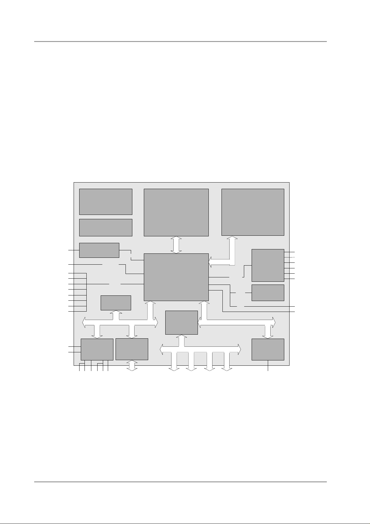
2 Overview
2.1 Features
The CB4053 is a highly complex PC/104-Plus board which incorporates complete motherboard
functionality. Equipped with an Intel® Atom™ processor (Z510 or Z530), it can accommodate up to 2
GByte of RAM (DDR2-533) via SO-DIMM200. It also provides a 16-bit ISA bus (via PC/104, no DMA and
memory transfer functions available) a PCI bus (via PC/104-Plus) and additional peripheral devices such
as two serial interfaces, Gigabit Ethernet interface (LAN), an IDE interface, an audio interface (HDA 7.1),
eight USB channels and CRT and LVDS/TFT support. As an option, the CB4053 can be equipped with an
onboard SSD of 2, 4 or 8GB capacity. The board is based on Intel®'s Menlow® platform which is
optimized for low power consumption. Relieving system designers of the burden that the need for active
cooling normally presents, Menlow® offers attractive new possibilities in the embedded and mobile
markets.
Power
VCCCore; VTT;
DDRVTT
1,5V; 1,8V; 2,5V; 3,3V
Clock
ICS9UMS9633
Intel® Atom™ CPU
Z510 / Z530
(1.1 GHz / 1.6 GHz)
1x SODIMM200
DDR2-RAM
(400/533MHz)
CRT
LCD
USB1
USB2
USB3
USB4
USB5
USB6
USB7
USB8
KB
MS
SDVO-to-RGB-
DAC (CH7317A)
LVDS 18/24
Winbond®
W83627HG
LPT
FAN 1
FAN 2
COM1
COM2
USB 2.0
BIOS
Watchdog
SDVO
US15W Chipset
LPC
Fintek®
F85226
LPC-to-ISA
PC/104
HOST
Intel® SCH
Pericom®
PI7C9X110
PCIe-to-PCI
Slot 1
PC/104plus
MEMORY
HDA-Link
master
slave
PCIe
PCI
Slot 2
Slot 3
Slot 4
PC/104plus
PC/104plus
PC/104plus
RealTek®
ALC885/889
2/4/8GB
SSD
Intel®
82574L
LAN
o Processor Intel® Atom™ (single core, 512KB L2-cache, up to 1.6 GHz clock speed)
o Chipset Intel® SCH US15W with integrated graphics adapter
o SO-DIMM200 socket for one DDR2-533 module of up to 2 GByte
o Two serial interfaces COM1 and COM2
o LAN interface Ethernet 10/100/1000 (Base-T)
o IDE interface
o Option: 2, 4 or 8GB SSD onboard (IDE master. Soldering option: slave)
o PS2 keyboard / mouse interface
SPDIF i
SPDIF o
LINE IN
LINE OUT
MIC
AUX
IDE
SMBus
page 10 Beckhoff New Automation Technology CB4053
Page 11

Features Chapter: Overview
o LPT interface
o Eight USB 2.0 interfaces (7x host, 1x host/device)
o AWARD BIOS 6.10
o CRT connection
o LCD connection via LVDS 18/24Bit
o AC97/HDA compatible sound controller with SPDIF in and out
o RTC with external CMOS battery
o 5V single supply voltage
o ISA bus via PC/104 (full 16bit support, no DMA and memory transfer functionality)
o PCI bus via PC/104-Plus (max. four master devices)
o Size: 96 mm x 90 mm
Beckhoff New Automation Technology CB4053 page 11
Page 12

Chapter: Overview Specifications and Documents
2.2 Specifications and Documents
In making this manual and for further reading of technical documentation, the following documents,
specifications and web-pages were used and are recommended.
§ ISA Specification
IEEE996P
www.ieee.org
§ PC/104™ Specification
Version 2.5
www.pc104.org
§ PC/104-Plus™ Specification
Version 2.0
www.pc104.org
§ PCI Specification
Version 2.3 and 3.0
www.pcisig.com
§ ACPI Specification
Version 3.0
www.acpi.info
§ ATA/ATAPI Specification
Version 7 Rev. 1
www.t13.org
§ USB Specifications
www.usb.org
§ SM-Bus Specification
Version 2.0
www.smbus.org
§ Intel® Chipset Description
SCH Datasheet
www.intel.com
§ Intel® Chip Description
Atom® Datasheet
www.intel.com
§ Winbond® Chip Description
W83627HF
www.winbond-usa.com or www.winbond.com.tw
§ Fintek® Chip Description
F85226F Datasheet
www.fintek.com.tw
§ Intel® Chip Description
82574L Datasheet
www.intel.com
page 12 Beckhoff New Automation Technology CB4053
Page 13

Power Supply Chapter: Detailed Description
3 Detailed Description
3.1 Power Supply
The power supply of the hardware module is effected via the power connector. The board only requires
an operating voltage of 5 volt ± 5%.
3.2 CPU
The motherboard employs an Intel® Atom™ processor either with 1.1GHz or with 1.6GHz clock speed
(Z510/Z530). These are single core CPUs which are optimized for low power consumption while at the
same time providing state-of-the-art computing performance.
The processors include a second level cache of 512 KByte. They also offer many features known from
the desktop range such as MMX2, serial number, loadable microcode etc.
The Atom™ CPU is combined with the SCH US15W chipset. The power consumption of these two
components never exceeds 5 watts combined. Therefore, passive cooling solutions will be sufficient for
many system configurations.
3.3 Memory
There is one conventional SO-DIMM200 socket available to equip the board with memory. For technical
and mechanical reasons it is possible that particular memory modules cannot be employed. Please ask
your sales representative for recommended memory modules.
With currently available SO-DIMM200 modules a memory extension up to 2 GByte is possible
(DDR2-533).
NOTE
The chip set does not support more than 2GB of memory.
Beckhoff New Automation Technology CB4053 page 13
Page 14

Chapter: Connectors Memory
4 Connectors
This section describes all the connectors found on the CB4053.
CAUTION
For most interfaces, the cables must meet certain requirements. For instance, USB 2.0 requires twisted
and shielded cables to reliably maintain full speed data rates. Restrictions on maximum cable length are
also in place for many high speed interfaces and for power supply. Please refer to the respective
specifications and use suitable cables at all times.
page 14 Beckhoff New Automation Technology CB4053
Page 15
Connector Map Chapter: Connectors
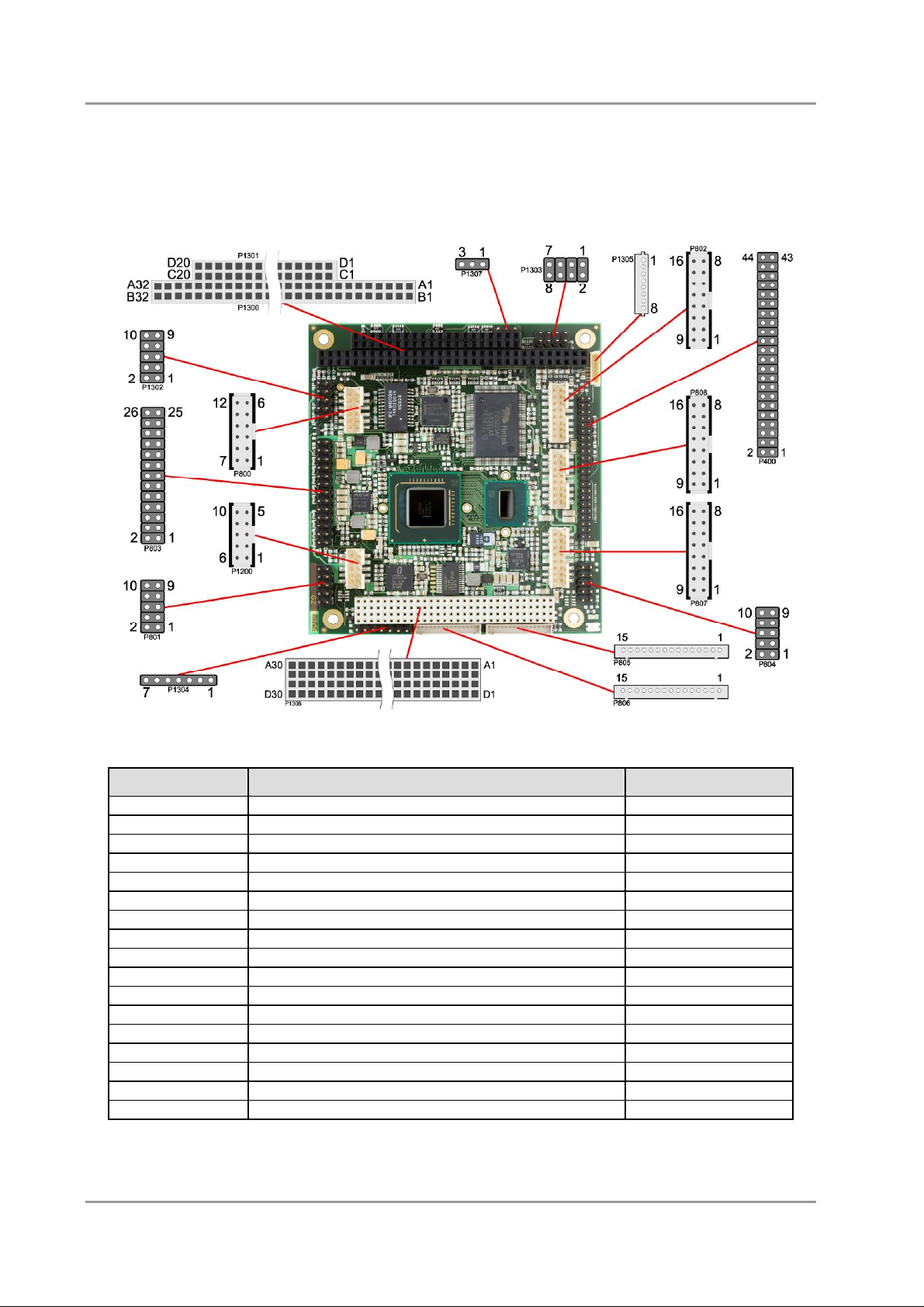
4.1 Connector Map
Please use the connector map below for quick reference. Only connectors on the component side are
shown. For more information on each connector refer to the table below.
Ref-No. Function Page
P400 "IDE Interface" p. 32
U500* "Memory" p. 18
P800** "LAN" p. 30
P801 "Serial Interface COM1" p. 35
P802** "Audio" p. 31
P803 "Parallel Interface LPT" p. 34
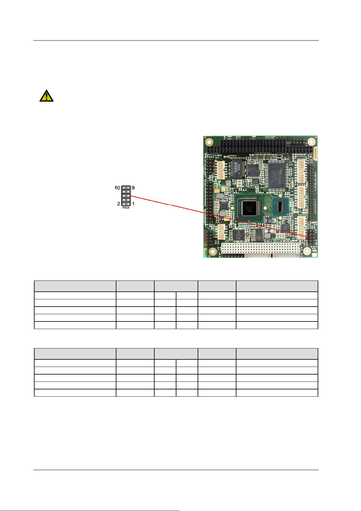
P804 "Serial Interface COM2" p. 36
P805/6 "LCD" p. 26
P807/8** "USB" p. 28
P1200** "VGA" p. 25
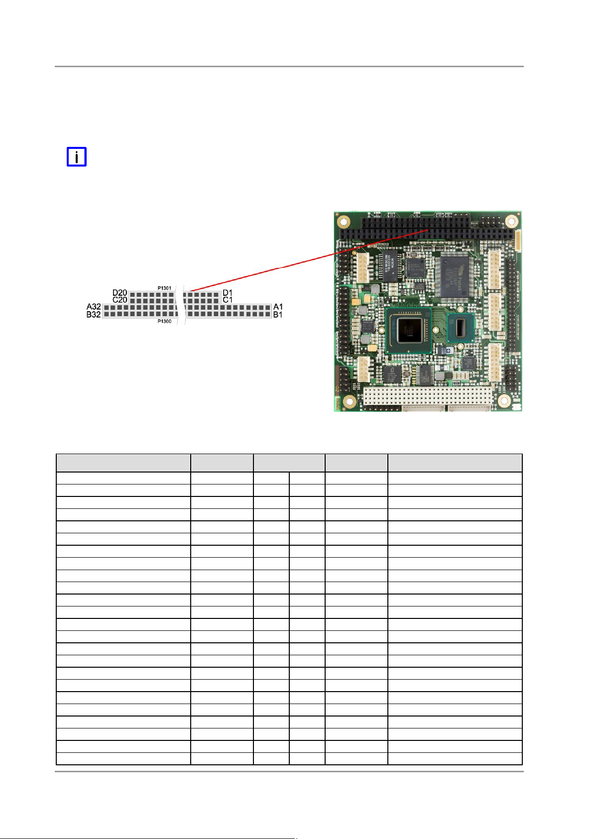
P1300/1 "PC/104-Bus" p. 21
P1302 "System" p. 17
P1303 "Power Supply" p. 16
P1304 "SMBus" p. 37
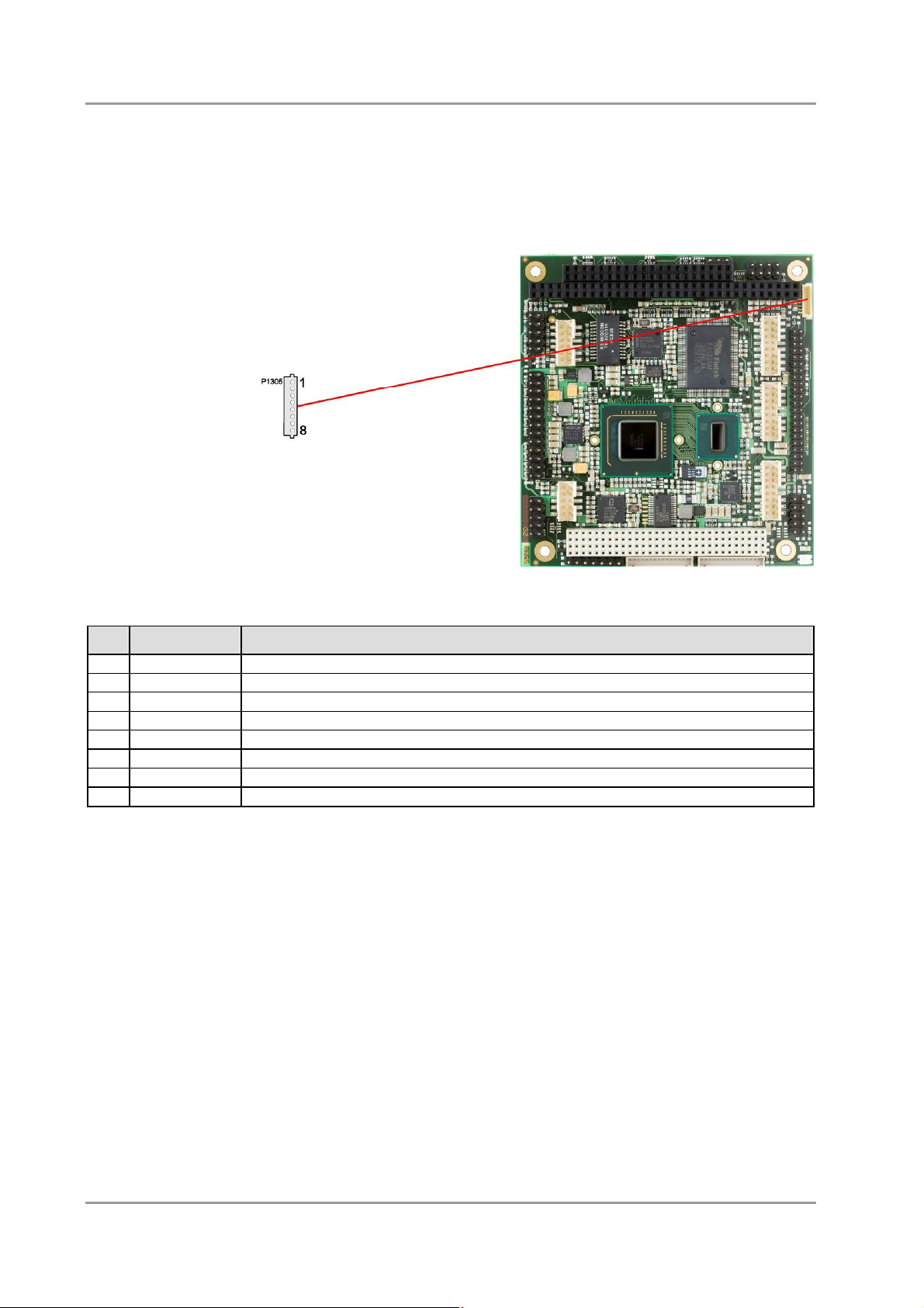
P1305 "Monitoring Functions" p. 38
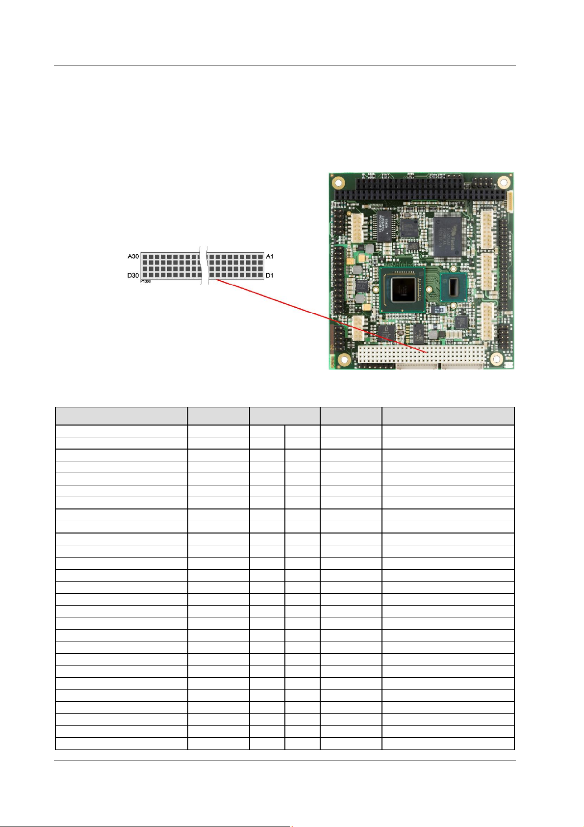
P1306 "PC/104-Plus Bus" p. 23
P1307 "Fan" p. 39
* not in the picture above (cf. bottom side of board)
** pin orientation holds for board revision G2 and later
Beckhoff New Automation Technology CB4053 page 15
Page 16
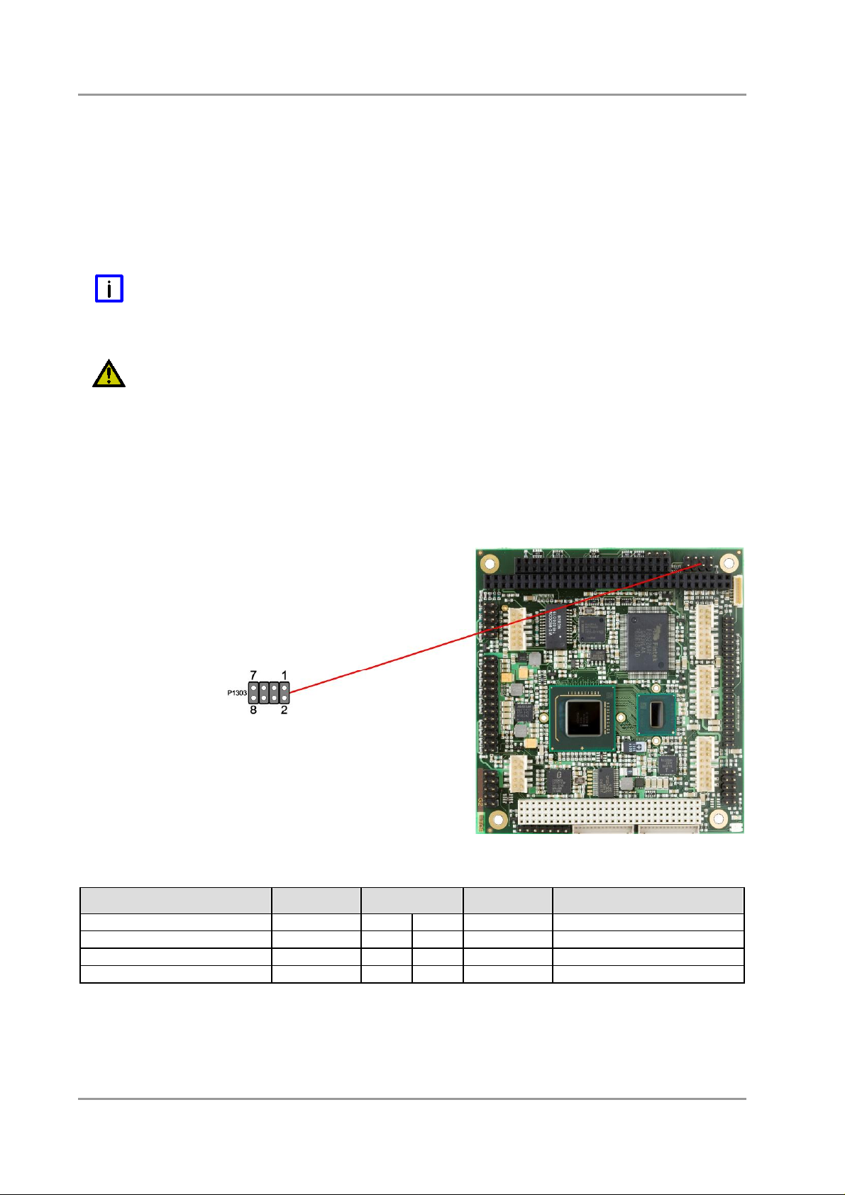
Chapter: Connectors Power Supply
4.2 Power Supply
The connector for the power supply is a standard IDC socket connector with a spacing of 2.54 mm.
The board only requires an operating voltage of 5 volt ± 5%. 3.3V output to the PC/104-Plus bus is the
only off-board supply available.
Should additional voltages be needed for PC/104 expansion cards, these must be provided externally by
connecting the respective pins (see below).
For maximum current availability, it is recommended to use both this power connector and the PC/104
connector for power supply.
NOTE
For "Real Time Clock" an external battery (3.3V) must be connected. You can use pins 1 & 3 here or the
"System" connector (see next page).
CAUTION
The CB4053 includes circuitry that will notify an intelligent power supply to shut down if the processor
reaches a critical temperature. This is achieved by deasserting the (low-active) PS_ON# signal found on
the SM-Bus connector. When PS_ON# is no longer pulled low, an intelligent power supply would take this
as a signal to shut down power. For this to work, PS_ON# must be connected to the power supply's
PS_ON input. If PS_ON# is not otherwise connected, the CB4053 can be damaged beyond repair if a
thermal shutdown event occurs. In rare instances, if power is not shut down, the board will continue to
heat up until failure occurs.
Description Name Pin Name Description
ground GND 1 2 VCC 5 volt supply
CMOS battery >= 3 volt VBAT 3 4 12V 12 volt supply
-5 volt supply -5V 5 6 -12V -12 volt supply
ground GND 7 8 VCC 5 volt supply
page 16 Beckhoff New Automation Technology CB4053
Page 17
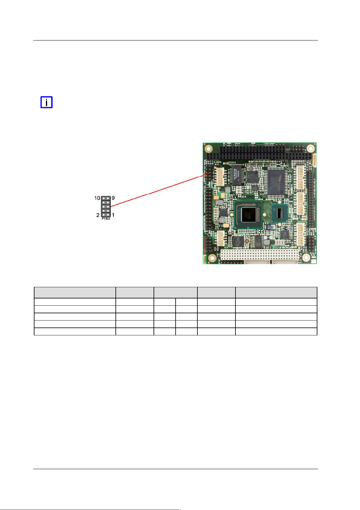
System Chapter: Connectors
4.3 System
The system connector, which has the main functions that are necessary to start the board, is provided via
a standard IDC socket connector with a spacing of 2.54 mm.
This connector supports the following interfaces: PS/2 keyboard, PS/2 mouse, speaker, external
RTC-battery and reset of the board.
NOTE
For "Real Time Clock" an external battery (3.3V) must be connected. Connect "+" to VBAT and "-" to
GND.
Description Name Pin Name Description
speaker to 5 volt SPEAKER 1 2 GND ground
reset to ground RESET# 3 4 KLOCK# keyboard lock
keyboard Data KDAT 5 6 KCLK keyboard clock
mouse data MDAT 7 8 MCLK mouse clock
CMOS battery ≥ 3 volt VBAT 9 10 VCC 5 volt supply
Beckhoff New Automation Technology CB4053 page 17
Page 18
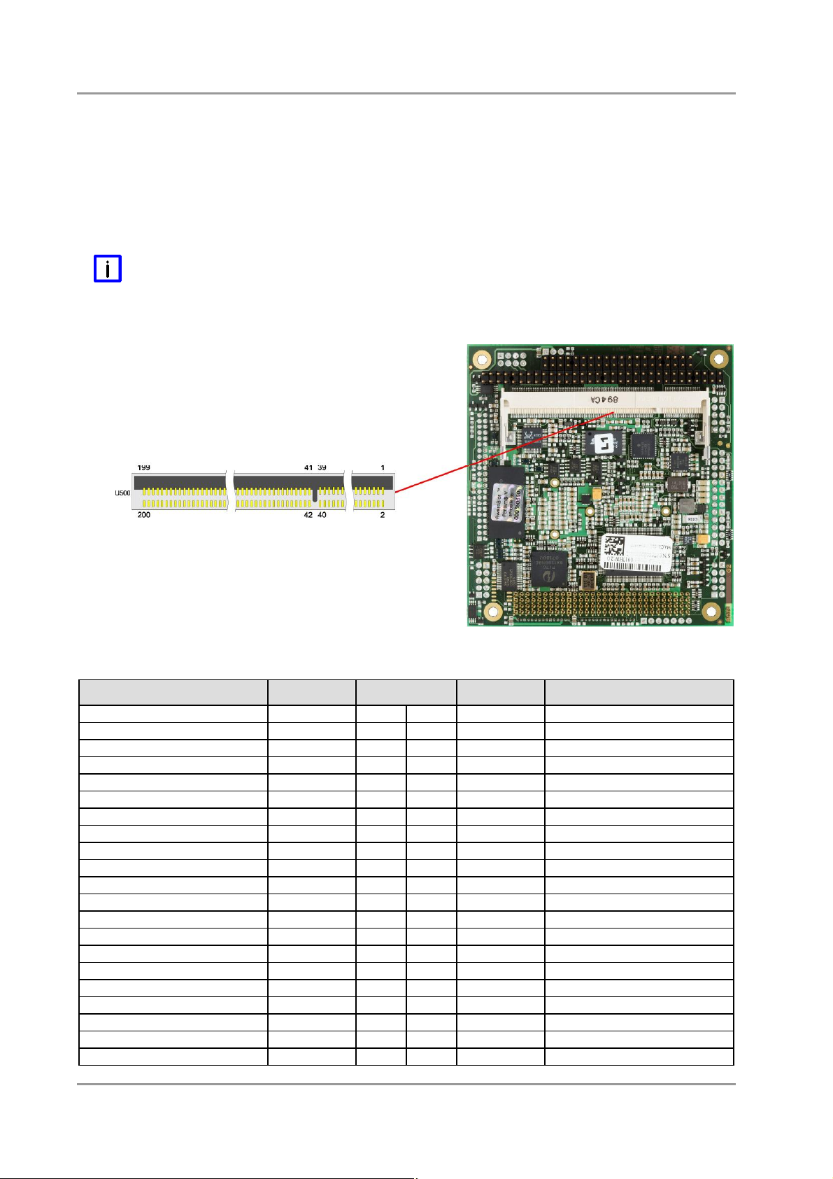
Chapter: Connectors Memory
4.4 Memory
There is one conventional SO-DIMM200 socket available to equip the board with memory (DDR2-533). It
is located on the bottom side of the board. For technical and mechanical reasons it is possible that
particular memory modules cannot be employed. Please ask your sales representative for recommended
memory modules.
With currently available SO-DIMM modules a memory extension up to 2 GByte is possible. The timing
parameters for different memory modules are automatically set by BIOS.
NOTE
The chip set does not support more than 2GB of memory.
Description Name Pin Name Description
memory reference current REF 1 2 REF memory reference current
ground GND 3 4 GND ground
data 0 DQ0 5 6 DQ4 data 4
data 1 DQ1 7 8 DQ5 data 5
2.5 volt supply 2.5V 9 10 2.5V 2.5 volt supply
data strobe 0 DQS0 11 12 DQM0 data mask 0
data 2 DQ2 13 14 DQ6 data 6
ground GND 15 16 GND ground
data 3 DQ3 17 18 DQ7 data 7
data 8 DQ8 19 20 DQ12 data 12
2.5 volt supply 2.5V 21 22 2.5V 2.5 volt supply
data 9 DQ9 23 24 DQ13 data 13
data strobe 1 DQS1 25 26 DQM1 data mask 1
ground GND 27 28 GND ground
data 10 DQ10 29 30 DQ14 data 14
data 11 DQ11 31 32 DQ15 data 15
2.5 volt supply 2.5V 33 34 2.5V 2.5 volt supply
clock CK0 35 36 2.5V 2.5 volt supply
clock CK0# 37 38 2.5V 2.5 volt supply
ground GND 39 40 GND ground
data 16 DQ16 41 42 DQ20 data 20
page 18 Beckhoff New Automation Technology CB4053
Page 19

Memory Chapter: Connectors
Description Name Pin Name Description
data 17 DQ17 43 44 DQ21 data 21
2.5 volt supply 2.5V 45 46 2.5V 2.5 volt supply
data strobe 2 DQS2 47 48 DQM2 data mask 2
data 18 DQ18 49 50 DQ22 data 22
ground GND 51 52 GND ground
data 19 DQ19 53 54 DQ23 data 23
data 24 DQ24 55 56 DQ28 data 28
2.5 volt supply 2.5V 57 58 2.5V 2.5 volt supply
data 25 DQ25 59 60 DQ29 data 29
data strobe 3 DQS3 61 62 DQM3 data mask 3
ground GND 63 64 GND ground
data 26 DQ26 65 66 DQ30 data 30
data 27 DQ27 67 68 DQ31 data 31
2.5 volt supply 2.5V 69 70 2.5V 2.5 volt supply
data check bit 0 CB0 71 72 CB4 data check bit 4
data check bit 1 CB1 73 74 CB5 data check bit 5
ground GND 75 76 GND ground
data strobe 8 DQS8 77 78 DQM8 data mask 8
data check bit 2 CB2 79 80 CB6 data check bit 6
2.5 volt supply 2.5V 81 82 2.5V 2.5 volt supply
data check bit 3 CB3 83 84 CB7 data check bit 7
reserved N/C 85 86 N/C reserved
ground GND 87 88 GND ground
clock CK2 89 90 GND ground
clock CK2# 91 92 2.5V 2.5 volt supply
2.5 volt supply 2.5V 93 94 2.5V 2.5 volt supply
clock enables 1 CKE1 95 96 CKE0 clock enables 0
reserved N/C 97 98 N/C reserved
address 12 A12 99 100 A11 address 11
address 9 A9 101 102 A8 address 8
ground GND 103 104 GND ground
address 7 A7 105 106 A6 address 6
address 5 A5 107 108 A4 address 4
address 3 A3 109 110 A2 address 2
address 1 A1 111 112 A0 address 0
2.5 volt supply 2.5V 113 114 2.5V 2.5 volt supply
address 10 A10 115 116 BA1 SDRAM bank 1
SDRAM bank 0 BA0 117 118 RAS# row address strobe
write enable WE# 119 120 CAS# column address strobe
chip select S0# 121 122 S1# chip select
reserved N/C 123 124 N/C reserved
ground GND 125 126 GND ground
data 32 DQ32 127 128 DQ36 data 36
data 33 DQ33 129 130 DQ37 data 37
2.5 volt supply 2.5V 131 132 2.5V 2.5 volt supply
data strobe 4 DQS4 133 134 DQM4 data mask 4
data 34 DQ34 135 136 DQ38 data 38
ground GND 137 138 GND ground
data 35 DQ35 139 140 DQ39 data 39
data 40 DQ40 141 142 DQ44 data 44
2.5 volt supply 2.5V 143 144 2.5V 2.5 volt supply
data 41 DQ41 145 146 DQ45 data 45
data strobe 5 DQS5 147 148 DQM5 data mask 5
ground GND 149 150 GND ground
data 42 DQ42 151 152 DQ46 data 46
Beckhoff New Automation Technology CB4053 page 19
Page 20

Chapter: Connectors Memory
Description Name Pin Name Description
data 43 DQ43 153 154 DQ47 data 47
2.5 volt supply 2.5V 155 156 2.5V 2.5 volt supply
2.5 volt supply 2.5V 157 158 CK1# clock
ground GND 159 160 CK1 clock
ground GND 161 162 GND ground
data 48 DQ48 163 164 DQ52 data 52
data 49 DQ49 165 166 DQ53 data 53
2.5 volt supply 2.5V 167 168 2.5V 2.5 volt supply
data strobe 6 DQS6 169 170 DQM6 data mask 6
data 50 DQ50 171 172 DQ54 data 54
ground GND 173 174 GND ground
data 51 DQ51 175 176 DQ55 data 55
data 56 DQ56 177 178 DQ60 data 60
2.5 volt supply 2.5V 179 180 2.5V 2.5 volt supply
data 57 DQ57 181 182 DQ61 data 61
data strobe 7 DQS7 183 184 DQM7 data mask 7
ground GND 185 186 GND ground
data 58 DQ58 187 188 DQ62 data 62
data 59 DQ59 189 190 DQ63 data 63
2.5 volt supply 2.5V 191 192 2.5V 2.5 volt supply
SPD data SDA 193 194 SA0 SPD address
SPD clock SCL 195 196 SA1 SPD address
3.3 volt supply 3.3V 197 198 SA2 SPD address
reserved N/C 199 200 N/C reserved
page 20 Beckhoff New Automation Technology CB4053
Page 21
PC/104-Bus Chapter: Connectors
4.5 PC/104-Bus
An onboard LPC-to-ISA bridge (Fintek® F85226F) makes it possible to expand the functionality of the
board with additional PC/104 cards. This interface offers full 16bit ISA compliance. For further information
on this interface please refer to the PC/104 specifications (see "Specifications and Documents", p. 12).
NOTE
The chipset used on this board does not support ISA-DMA functionality.
Pinning of the standard 8 bit PC/104 connector.
Description Name Pin Name Description
ISA - IO channel check IOCHK# A1 B1 GND ground
ISA – data 7 SD7 A2 B2 RSTDRV reset drive
ISA – data 6 SD6 A3 B3 VCC 5 volt supply
ISA – data 5 SD5 A4 B4 IRQ9 ISA – interrupt 9 (2)
ISA – data 4 SD4 A5 B5 -5V -5 volt supply
ISA – data 3 SD3 A6 B6 (DRQ2) reserved
ISA – data 2 SD2 A7 B7 -12V -12 volt supply
ISA – data 1 SD1 A8 B8 IOCHRDY ISA – IO channel ready
ISA – data 0 SD0 A9 B9 12V 12 volt supply
ISA – IO channel ready IOCHRDY A10 B10 N/C reserved
ISA – address enable AEN A11 B11 SMEMW# ISA – system memory write
ISA – address 19 SA19 A12 B12 SMEMR# ISA – system memory read
ISA – address 18 SA18 A13 B13 IOW# ISA – IO write
ISA – address 17 SA17 A14 B14 IOR# ISA – IO read
ISA – address 16 SA16 A15 B15 (DACK3#) reserved (pulled high)
ISA – address 15 SA15 A16 B16 (DRQ3) reserved
ISA – address 14 SA14 A17 B17 (DACK1#) reserved (pulled high)
ISA – address 13 SA13 A18 B18 (DRQ1) reserved
ISA – address 12 SA12 A19 B19 REFRESH# ISA – refresh
ISA – address 11 SA11 A20 B20 SYSCLK ISA – system clock
ISA – address 10 SA10 A21 B21 IRQ7 ISA – interrupt 7
ISA – address 9 SA9 A22 B22 IRQ6 ISA – interrupt 6
ISA – address 8 SA8 A23 B23 IRQ5 ISA – interrupt 5
ISA – address 7 SA7 A24 B24 IRQ4 ISA – interrupt 4
Beckhoff New Automation Technology CB4053 page 21
Page 22

Chapter: Connectors PC/104-Bus
Description Name Pin Name Description
ISA – address 6 SA6 A25 B25 IRQ3 ISA – interrupt 3
ISA – address 5 SA5 A26 B26 (DACK2#) reserved (pulled high)
ISA – address 4 SA4 A27 B27 T/C ISA – terminal count
ISA – address 3 SA3 A28 B28 BALE ISA – address latch en.
ISA – address 2 SA2 A29 B29 VCC 5 volt supply
ISA – address 1 SA1 A30 B30 OSC ISA – 14,318MHz
ISA – address 0 SA0 A31 B31 GND ground
ground GND A32 B32 GND ground
Pinning of the 16 bit expansion PC/104 connector.
Description Name Pin Name Description
ground GND C0 D0 GND ground
ISA – byte high enable SBHE# C1 D1 MEMCS16# ISA – memory chip select
ISA – latched address 23 LA23 C2 D2 IOCS16# ISA – IO chip select
ISA – latched address 22 LA22 C3 D3 IRQ10 ISA – interrupt 10
ISA – latched address 21 LA21 C4 D4 IRQ11 ISA – interrupt 11
ISA – latched address 20 LA20 C5 D5 IRQ12 ISA – interrupt 12
ISA – latched address 19 LA19 C6 D6 IRQ15 ISA – interrupt 15
ISA – latched address 18 LA18 C7 D7 IRQ14 ISA – interrupt 14
ISA – latched address 17 LA17 C8 D8 (DACK0#) reserved (pulled high)
ISA – memory read MEMR# C9 D9 (DRQ0) reserved
ISA – memory write MEMW# C10 D10 (DACK5#) reserved (pulled high)
ISA – data 8 SD8 C11 D11 (DRQ5) reserved
ISA – data 9 SD9 C12 D12 (DACK6#) reserved (pulled high)
ISA – data 10 SD10 C13 D13 (DRQ6) reserved
ISA – data 11 SD11 C14 D14 (DACK7#) reserved (pulled high)
ISA – data 12 SD12 C15 D15 (DRQ7) reserved
ISA – data 13 SD13 C16 D16 VCC 5 volt supply
ISA – data 14 SD14 C17 D17 MASTER# ISA – bus master
ISA – data 15 SD15 C18 D18 GND ground
reserved N/C C19 D19 GND ground
page 22 Beckhoff New Automation Technology CB4053
Page 23
PC/104-Plus Bus Chapter: Connectors
4.6 PC/104-Plus Bus
Expansion cards can be connected to the board using the PCI connector first introduced with the
PC/104-Plus standard. A maximum of four PC/104-Plus cards are supported.
The interrupt routing and the IDSEL signals for the expansion cards are specified in the PC/104-Plus
specification (see "Specifications and Documents", p. 12).
Description Name Pin Name Description
ground GND A1 B1 N/C reserved
3.3 volt - IO buffer power VIO A2 B2 AD2 PCI – address/data 2
PCI – address/data 5 AD5 A3 B3 GND ground
PCI – com/byte enable 0 CBE0# A4 B4 AD7 PCI – address/data 7
ground GND A5 B5 AD9 PCI – address/data 9
PCI – address/data 11 AD11 A6 B6 VIO 3.3 volt - IO buffer power
PCI – address/data 14 AD14 A7 B7 AD13 PCI – address/data 13
3.3 volt supply 3.3V A8 B8 CBE1# PCI – com/byte enable 1
PCI – system error SERR# A9 B9 GND ground
ground GND A10 B10 PERR# PCI – parity error
PCI – stop stop# A11 B11 3.3V 3.3 volt supply
3.3 volt supply 3.3V A12 B12 TRDY# PCI – target ready
PCI – frame FRAME# A13 B13 GND ground
ground GND A14 B14 AD16 PCI – address/data 16
PCI – address/data 18 AD18 A15 B15 3.3V 3.3 volt supply
PCI – address/data 21 AD21 A16 B16 AD20 PCI – address/data 20
3.3 volt supply 3.3V A17 B17 AD23 PCI – address/data 23
PCI – ID select slot 1 IDSEL0 A18 B18 GND ground
PCI – address/data 24 AD24 A19 B19 CBE3# PCI – com/byte enable 3
ground GND A20 B20 AD26 PCI – address/data 26
PCI – address/data 29 AD29 A21 B21 VCC 5 volt supply
5 volt supply VCC A22 B22 AD30 PCI – address/data 30
PCI – bus request slot 1 REQ0# A23 B23 GND ground
ground GND A24 B24 REQ2# PCI – bus request slot 3
PCI – bus grant slot 4 GNT1# A25 B25 VIO 5 volt - IO buffer power
5 volt supply VCC A26 B26 CLK0 PCI – clock slot 1
PCI – clock slot 3 CLK2 A27 B27 VCC 5 volt supply
Beckhoff New Automation Technology CB4053 page 23
Page 24

Chapter: Connectors PC/104-Plus Bus
Description Name Pin Name Description
ground GND A28 B28 INTD# PCI – interrupt D
12V supply 12V A29 B29 INTA# PCI – interrupt A
-12V supply -12V A30 B30 REQ3# PCI – bus request slot 4
5 volt supply VCC C1 D1 AD0 PCI – address/data 0
PCI – address/data 1 AD1 C2 D2 VCC 5 volt supply
PCI – address/data 4 AD4 C3 D3 AD3 PCI – address/data 3
ground GND C4 D4 AD6 PCI – address/data 6
PCI – address/data 8 AD8 C5 D5 GND ground
PCI – address/data 10 AD10 C6 D6 M66EN PCI – 66MHz enable
ground GND C7 D7 AD12 PCI – address/data 12
PCI – address/data 15 AD15 C8 D8 3.3V 3.3 volt supply
reserved N/C C9 D9 PAR PCI – parity bit
3.3 volt supply 3.3V C10 D10 N/C reserved
PCI – lock LOCK# C11 D11 GND ground
ground GND C12 D12 DEVSEL# PCI – device select
PCI – initiator ready IRDY# C13 D13 3.3V 3.3 volt supply
3.3 volt supply 3.3V C14 D14 CBE2# PCI – com/byte enable 2
PCI – address/data 17 AD17 C15 D15 GND ground
ground GND C16 D16 AD19 PCI – address/data 19
PCI – address/data 22 AD22 C17 D17 3.3V 3.3 volt supply
PCI – ID select slot 2 IDSEL1 C18 D18 IDSEL2 PCI – ID select slot 3
3,3 volt - IO buffer power VIO C19 D19 IDSEL3 PCI – ID select slot 4
PCI – address/data 25 AD25 C20 D20 GND ground
PCI – address/data 28 AD28 C21 D21 AD27 PCI – address/data 27
ground GND C22 D22 AD31 PCI – address/data 31
PCI – bus request slot 2 REQ1# C23 D23 VIO 3,3 volt - IO buffer power
5 volt supply VCC C24 D24 GNT0# PCI – bus grant slot 1
PCI – bus grant slot 3 GNT2# C25 D25 GND ground
ground GND C26 D26 CLK1 PCI – clock slot 2
PCI – clock slot 4 CLK3 C27 D27 GND ground
5 volt supply VCC C28 D28 RST# PCI – reset
PCI – interrupt B INTB# C29 D29 INTC# PCI – interrupt C
PCI – bus grant slot 4 GNT3# C30 D30 GND ground
page 24 Beckhoff New Automation Technology CB4053
Page 25
VGA Chapter: Connectors
4.7 VGA
The CRT-VGA signals are provided by a 2x5pin connector (FCI 98424-G52-10LF, mating connector e.g.
FCI 90311-010LF).
This interface allows the connection of a standard VGA-monitor. I2C communication is supported.
Description Name Pin Name Description
analog red RED 1 6 GND ground
analog green GREEN 2 7 DDDA DD data
analog blue BLUE 3 8 DDCK DD clock
vertikal sync VSYNC 4 9 GND ground
horizontal sync HSYNC 5 10 GND ground
Beckhoff New Automation Technology CB4053 page 25
Page 26

Chapter: Connectors LCD
4.8 LCD
The LCD is connected via two 15 pin connectors (Hirose DF13-15P-1.25DSA, mating connector:
DF13-15S-xxx). The power supply for the display is also provided through these connectors. The CB4053
board only supports displays with LVDS interface. For displays with digital interface an extra receiver
board is available. There is no support for DSTN displays.
With the LVDS interface it is possible to trigger LVDS displays with a maximum of 24 Bit colour depth
and one pixel per clock. The second connector provides an interface to the display's EDID data, and can
be left unconnected if EDID data are not required.
The display type can be chosen over the BIOS setup. Please contact your sales representative regarding
an appropriate cable to connect your display.
The following table shows the pin description for the first bit ("even" pixel).
Pin
Name Description
1 GND ground
2 GND ground
3 TXO00# LVDS even data 0 4 TXO00 LVDS even data 0 +
5 TXO01# LVDS even data 1 6 TXO01 LVDS even data 1 +
7 TXO02# LVDS even data 2 8 TXO02 LVDS even data 2 +
9 TXO0C# LVDS even clock 10 TXO0C LVDS even clock +
11 TXO03# LVDS even data 3 12 TXO03 LVDS even data 3 +
13 BL_VCC switched 5 volt for backlight
14 FP_3.3V switched 3.3 volt for display
15 FP_3.3V switched 3.3 volt for display
page 26 Beckhoff New Automation Technology CB4053
Page 27

LCD Chapter: Connectors
The following table shows the pin description for the second connector used for evaluating the display's
EDID data.
Pin
Name Description
1 GND ground
2 GND ground
3 N/C reserved
4 N/C reserved
5 N/C reserved
6 N/C reserved
7 N/C reserved
8 N/C reserved
9 N/C reserved
10 N/C reserved
11 N/C reserved
12 N/C reserved
13 DDC_CLK EDID clock for LCD
14 DDC_DAT EDID data for LCD
15 VCC 5 volt supply
Beckhoff New Automation Technology CB4053 page 27
Page 28

Chapter: Connectors USB
4.9 USB
USB channels 1 to 8 are provided via two 2x8pin connectors (FCI 98424-G52-16LF, mating connector
e.g. FCI 90311-016LF).
All USB-channels support USB 2.0. You may note that the setting of USB keyboard or USB mouse
support in the BIOS-setup is only necessary and advisable, if the OS offers no USB-support. BIOS-setup
can be changed with a USB keyboard without enabling USB keyboard support. Running a USB
supporting OS (such as Microsoft® Windows®) with these features enabled may lead to significant
performance or functionality limitations.
Every USB interface provides up to 500 mA current and is protected by an electronically resettable fuse.
NOTE
USB channel 3 can be configured to run in "device" mode. USB channels 7 and 8 do not support
USB1.0/1.1.
Pinout USB 1-4:
Description Name Pin Name Description
5 volt for USB1 USB1 VCC 1 9 USB2VCC 5 volt for USB2
minus channel USB1 USB1# 2 10 USB2# minus channel USB2
plus channel USB1 USB1 3 11 USB2 plus channel USB2
ground GND 4 12 GND ground
ground GND 5 13 GND ground
plus channel USB3 USB3 6 14 USB4 plus channel USB4
minus channel USB3 USB3# 7 15 USB4# minus channel USB4
5 volt for USB3 USB3VCC 8 16 USB4VCC 5 volt for USB4
page 28 Beckhoff New Automation Technology CB4053
Page 29

USB Chapter: Connectors
Pinout USB 5-8:
Description Name Pin Name Description
5 volt for USB5 USB5 VCC 1 9 USB6VCC 5 volt for USB6
minus channel USB5 USB5# 2 10 USB6# minus channel USB6
plus channel USB5 USB5 3 11 USB6 plus channel USB6
ground GND 4 12 GND ground
ground GND 5 13 GND ground
plus channel USB7 USB7 6 14 USB8 plus channel USB8
minus channel USB7 USB7# 7 15 USB8# minus channel USB8
5 volt for USB7 USB7VCC 8 16 USB8VCC 5 volt for USB8
Beckhoff New Automation Technology CB4053 page 29
Page 30

Chapter: Connectors LAN
4.10 LAN
The LAN interface is provided via a 2x6pin connector (FCI 98424-G52-12LF, mating connector e.g. FCI
90311-012LF). The interface supports 10BaseT, 100BaseT, and 1000BaseT compatible network
components with automatic bandwidth selection. Additional outputs are provided for status LEDs.
Auto-negotiate and auto-cross functionality is available, PXE and RPL are available on request.
Pinout LAN interface:
Description Name Pin Name Description
LAN activity LINKACT 1 7 SPEED1000 LAN speed 1000Mbit
LAN channel 1 plus LAN1 2 8 LAN0 LAN channel 0 plus
LAN channel 1 minus LAN1# 3 9 LAN0# LAN channel 0 minus
LAN channel 3 plus LAN3 4 10 LAN2 LAN channel 2 plus
LAN channel 3 minus LAN3# 5 11 LAN2# LAN channel 2 minus
LAN speed 100Mbit SPEED100 6 12 3.3V 3.3 volt supply
page 30 Beckhoff New Automation Technology CB4053
Page 31

Audio Chapter: Connectors
4.11 Audio
The CB4053's audio functions are provided via a 2x8pin connector (FCI 98424-G52-16LF, mating
connector e.g. FCI 90311-016LF). This interface provides eight output channels for full 7.1 sound output.
Two microphone inputs and two AUX inputs are also available.
The signals "SPDIFI" and "SPDIFO" provide digital input and output. If a transformation to a coaxial or
optical connector is necessary this must be performed externally.
Description Name Pin Name Description
digital output SPDIF SPDIFO 1 9 3.3V 3.3 volt supply
digital input SPDIF SPDIFI 2 10 S_AGND analog ground sound
sound output right LOUT_R 3 11 LOUT_L sound output left
AUX input right AUXA_R 4 12 AUXA_L AUX input left
microphone input 1 MIC1 5 13 MIC2 microphone input 2
surround out right SOUT_R 6 14 SOUT_L surround out left
center output CENOUT 7 15 LFEOUT LFE output
side surround out right SSOUT_R 8 16 SSOUT_L side surround out left
Beckhoff New Automation Technology CB4053 page 31
Page 32

Chapter: Connectors IDE Interface
4.12 IDE Interface
The primary IDE interface is a standard IDC socket connector with a spacing of 2 mm. All commercial IDE
devices are supported but an adapter to connect may be necessary.
The required settings are made in the BIOS setup.
CAUTION
Pins are not keyed! Please be sure to connect the cable properly, otherwise you risk damaging the IDE
interface, the CPU and the drive, voiding respective warranties.
Pinout for primary IDE
Description Name Pin Name Description
reset PRST# 1 2 GND ground
data bit 7 PDD7 3 4 PDD8 data bit 8
data bit 6 PDD6 5 6 PDD9 data bit 9
data bit 5 PDD5 7 8 PDD10 data bit 10
data bit 4 PDD4 9 10 PDD11 data bit 11
data bit 3 PDD3 11 12 PDD12 data bit 12
data bit 2 PDD2 13 14 PDD13 data bit 13
data bit 1 PDD1 15 16 PDD14 data bit 14
data bit 0 PDD0 17 18 PDD15 data bit 15
ground GND 19 20 N/C reserved
DMA request signal PDDREQ 21 22 GND ground
write signal PDIOW# 23 24 GND ground
read signal PDIOR# 25 26 GND ground
ready signal PDRDY 27 28 N/C reserved
DMA acknowledge signal PDDACK# 29 30 GND ground
interrupt signal PDIRQ 31 32 N/C reserved
address bit 1 PDA1 33 34 PDMA66EN enable UDMA66
address bit 0 PDA0 35 36 PDA2 address bit 2
chip select signal 0 PDSC0# 37 38 PDCS1# chip select signal 1
LED PHDLED 39 40 GND ground
supply HDD 5V VCC 41 42 VCC supply HDD 5V
ground GND 43 44 N/C reserved
page 32 Beckhoff New Automation Technology CB4053
Page 33

IDE Interface Chapter: Connectors
CAUTION
If the board has a solid state disk (SSD) installed then you must not connect legacy IDE devices which
still use a signal level of 5V instead of 3.3V.
Beckhoff New Automation Technology CB4053 page 33
Page 34

Chapter: Connectors Parallel Interface LPT
4.13 Parallel Interface LPT
The parallel interface is a standard IDC socket connector with a spacing of 2.54 mm. The port address
and the interrupt are set via the BIOS setup.
Description Name Pin Name Description
strobe STB# 1 2 AFD# automatic line feed
LPT data 0 PD0 3 4 ERR# error
LPT data 1 PD1 5 6 INIT# init
LPT data 2 PD2 7 8 SLIN# select input
LPT data 3 PD3 9 10 GND ground
LPT data 4 PD4 11 12 GND ground
LPT data 5 PD5 13 14 GND ground
LPT data 6 PD6 15 16 GND ground
LPT data 7 PD7 17 18 GND ground
acknowledge ACK# 19 20 GND ground
busy BUSY 21 22 GND ground
paper end PE 23 24 GND ground
select printer SLCT 25 26 VCC 5 volt supply
page 34 Beckhoff New Automation Technology CB4053
Page 35
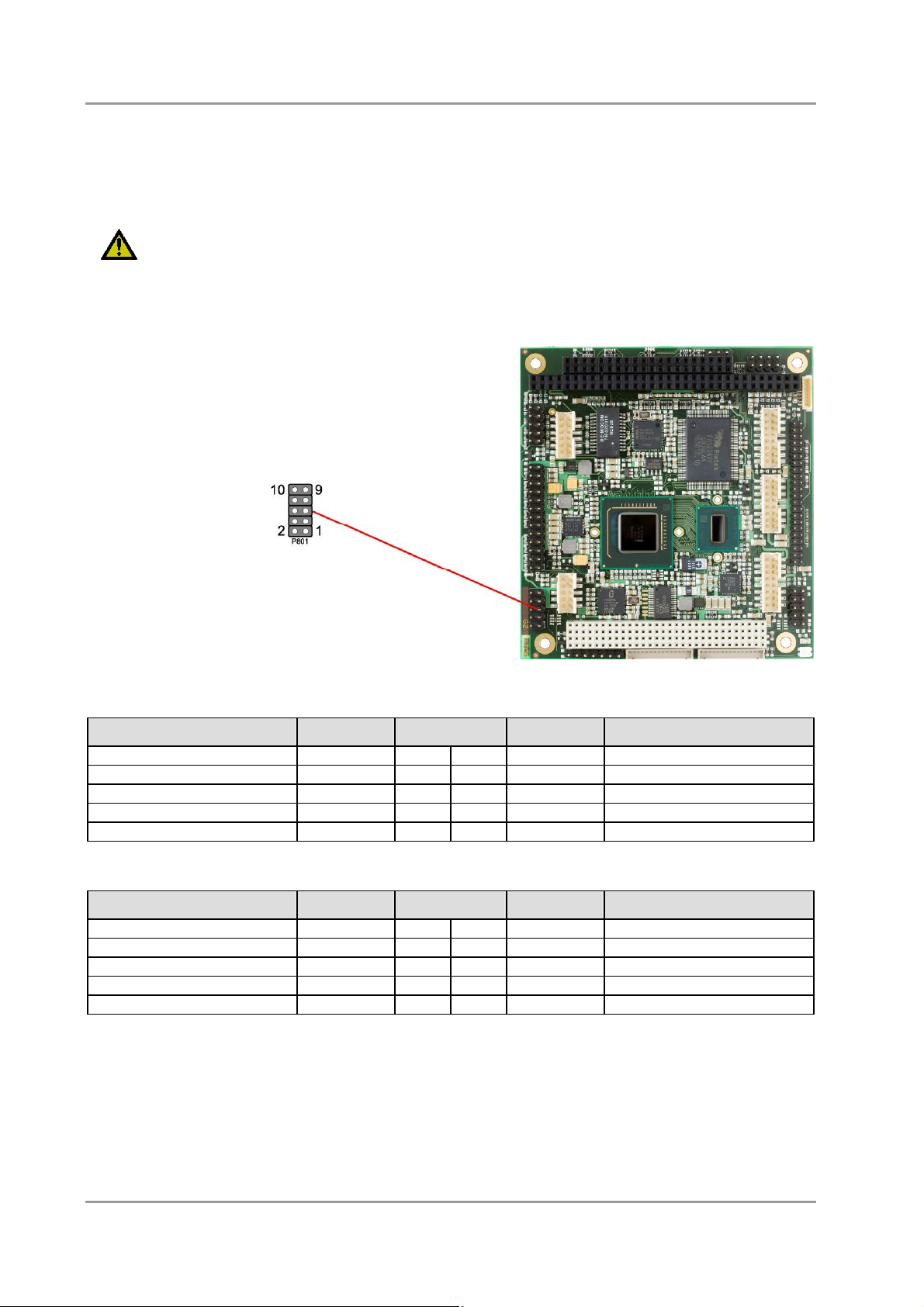
Serial Interface COM1 Chapter: Connectors
4.14 Serial Interface COM1
The serial interface is a standard IDC socket connector with a spacing of 2.54 mm. Signals default to
RS-232 but can also be ordered as RS-422 or RS-485.
The port address and the interrupt are set via the BIOS setup.
CAUTION
COM 1 & 2 cables are not the same pin orientation and you may damage the COM interface and CPU
attached if you use the incorrect COM cable.
Description Name Pin Name Description
data carrier detect DCD 1 2 DSR data set ready
receive data RXD 3 4 RTS request to send
transmit data TXD 5 6 CTS clear to send
data terminal ready DTR 7 8 RI ring indicator
ground GND 9 10 VCC 5 volt supply
Pinout with RS422/485 soldering option:
Description Name Pin Name Description
transmit data + TX 1 2 TX# transmit data receive data + RX 3 4 RX# receive data reserved N/C 5 6 N/C reserved
reserved N/C 7 8 N/C reserved
ground GND 9 10 VCC 5 volt supply
Beckhoff New Automation Technology CB4053 page 35
Page 36
Chapter: Connectors Serial Interface COM2
4.15 Serial Interface COM2
The serial interface is a standard IDC socket connector with a spacing of 2.54 mm. Signals default to
RS-232 but can also be ordered as RS-422 or RS-485.
The port address and the interrupt are set via the BIOS setup.
CAUTION
COM 1 & 2 cables are not the same pin orientation and you may damage the COM interface and CPU
attached if you use the incorrect COM cable.
Description Name Pin Name Description
data carrier detect DCD 1 2 DSR data set ready
receive data RXD 3 4 RTS request to send
transmit data TXD 5 6 CTS clear to send
data terminal ready DTR 7 8 RI ring indicator
ground GND 9 10 VCC 5 volt supply
Pinout with RS422/485 soldering option:
Description Name Pin Name Description
transmit data + TX 1 2 TX# transmit data receive data + RX 3 4 RX# receive data reserved N/C 5 6 N/C reserved
reserved N/C 7 8 N/C reserved
ground GND 9 10 VCC 5 volt supply
page 36 Beckhoff New Automation Technology CB4053
Page 37
SMBus Chapter: Connectors
4.16 SMBus
The CB4053 can communicate with external devices via the SMBus protocol. The signals for this protocol
are available through a standard IDC socket connector with a spacing of 2.54 mm. A 3.3 volt power
supply is also available for these SMBus devices. Additionally, you can use this connector to access the
PWRBTN# and PS_ON# signals used for power control. If PWRBTN# is held low for four seconds an
unconditional hardware power-down event will occur.
Pin
Name Description
1 3.3V 3.3 volt supply
2 CS-SMB-CLK SMBus clock
3 CS-SMB-DAT SMBus data
4 SMB-ALERT# SMBus alert
5 PWRBTN# power button
6 PS_ON# power supply on
7 GND ground
Beckhoff New Automation Technology CB4053 page 37
Page 38
Chapter: Connectors Monitoring Functions
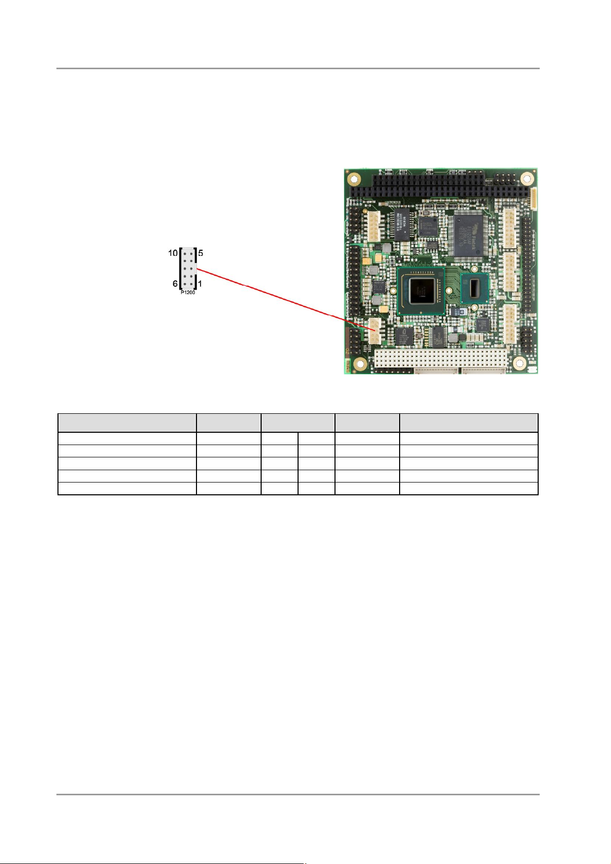
4.17 Monitoring Functions
Additional monitoring functions, such as the status of the fan or of other devices connected over SM-Bus
(e. g. temperature sensor), are accessible via an 8 pin connector (JST BM08B-SRSS-TB, mating
connector: SHR-08V-S(-B)).
Pin
Name Description
1 3.3V 3.3 volt supply
2 CS-SMB-CLK SMBus clock
3 CS-SMB-DAT SMBus data
4 GND ground
5 FANON1 5 volt supply (switched)
6 FANCTRL1 fan 1 monitoring signal
7 VCC 5 volt supply
8 FANCTRL3 fan 3 monitoring signal
page 38 Beckhoff New Automation Technology CB4053
Page 39

Fan Chapter: Connectors
4.18 Fan
A 3 pin connector is available for controlling and monitoring an external fan (5 volt). For the monitoring the
fan must provide a corresponding speed signal.
Pin
Name Description
1 GND ground
2 FANON2 5 volt supply (switched)
3 FANCTRL2 fan monitoring signal
Beckhoff New Automation Technology CB4053 page 39
Page 40

Chapter: Status LEDs HD LED
5 Status LEDs
5.1 HD LED
Harddisk activity is signalled by a dedicated LED.
page 40 Beckhoff New Automation Technology CB4053
Page 41

RGB LED Chapter: Status LEDs
The microcontroller has just been flashed and is being prepared for normal
5.2 RGB LED
The CB4053 has an RGB LED, which can signal status messages by using different colors and flash
intervals.
Status Codes RGB LED:
Color Interval Meaning
none solid Invalid system state
White solid
operation after reboot
Cyan solid Reserved
Magenta solid Reserved
Blue solid Reserved
Yellow solid Reserved
Green solid Board operates normal
Red solid Board is in Reset
Green/Yellow flashing Bootloader operates normal
Red flashing Firmware is being started (start sequence still running)
Red/Yellow flashing Bootloader is being started (start sequence still running)
Red/Magenta flashing Checksum error during I2C transmission in bootloader
Red/Blue flashing Update completed, waiting for manual Reset
Yellow flashing (10s) S5 state
Yellow flashing (6s) S4 state
Yellow flashing (3s) Reserved
Yellow flashing (0.5s) Reserved
Beckhoff New Automation Technology CB4053 page 41
Page 42

Chapter: BIOS Settings Remarks for Setup Use
6 BIOS Settings
6.1 Remarks for Setup Use
In a setup page, standard values for its setup entries can be loaded. Fail-safe defaults are loaded with F6
and optimized defaults are loaded with F7. These standard values are independent of the fact that a
board has successfully booted with a setup setting before.
This is different if these defaults are called from the Top Menu. Once a setup setting was saved, which
subsequently leads to a successful boot process, those values are loaded as default for all setup items
afterwards.
See also the chapters “Load Fail-Safe Defaults" (5.10) and “Load Optimized Defaults” (5.11).
NOTE
BIOS features and setup options are subject to change without notice. The settings displayed in the
screenshots on the following pages are meant to be examples only. They do not represent the
recommended settings or the default settings. Determination of the appropriate settings is dependent
upon the particular application scenario in which the board is used.
6.2 Top Level Menu
► Standard CMOS Features ► PC Health Status
► Advanced BIOS Features Load Fail-Safe Defaults
► Advanced Chipset Features Load Optimized Defaults
► Integrated Peripherals Set Password
► Power Management Setup Save & Exit Setup
► PnP/PCI Configurations Exit Without Saving
Esc : Quit ↑ ↓ → ← : Select Item
F10 : Save & Exit Setup
The sign „►“ in front of an item means that there is a sub menu.
The „x“ sign in front of an item means, that the item is disabled but can be enabled by changing or
selecting some other item (usually somewhere above the disabled item on the same screen).
Phoenix – AwardBIOS CMOS Setup Utility
"brief description of selected item"
Use the arrow buttons to navigate from one item to another. For selecting an item press Enter which will
open either a sub menu or a dialog screen.
page 42 Beckhoff New Automation Technology CB4053
Page 43

Standard CMOS Features Chapter: BIOS Settings
6.3 Standard CMOS Features
Date (mm:dd:yy) Thu, Feb 5 2009
Time (hh:mm:ss) 11 : 13 : 35
► IDE Channel 0 Master [4GB NANDrive]
► IDE Channel 0 Slave [ None]
Drive A [None]
Base Memory 639K
Extended Memory 1038336K
Total Memory 1039360K
↑↓→←:Move Enter:Select +/-/PU/PD:Value F10:Save ESC:Exit F1:Help
F5: Previous Values F6: Fail-Safe Defaults F7: Optimized Defaults
Phoenix – AwardBIOS CMOS Setup Utility
Standard CMOS Features
Item Help
ü Date (mm:dd:yy)
Options: mm: month
dd: day
yy: year
ü Time (hh:mm:ss)
Options: hh: hours
mm: minutes
ss: seconds
ü IDE Channel 0 Master
Sub menu: see "IDE Channel 0 Master/Slave" (p. 44)
ü IDE Channel 0 Slave
Sub menu: see "IDE Channel 0 Master/Slave" (p. 44)
ü Drive A
Options: None / 360K, 5.25 in. / 1.2M, 5.25 in. / 720K, 3.5 in. / 1.44M, 3.5 in. / 2.88M, 3.5 in.
ü Base Memory
Options: none
ü Extended Memory
Options: none
ü Total Memory
Options: none
Beckhoff New Automation Technology CB4053 page 43
Page 44

Chapter: BIOS Settings Standard CMOS Features
6.3.1 IDE Channel 0 Master/Slave
IDE HDD Auto-Detection [Press Enter]
IDE Channel 0 Master [Auto]
Access Mode [Auto]
Capacity 4096 MB
Cylinder 7937
Head 16
Precomp 0
Landing Zone 7936
Sector 63
↑↓→←:Move Enter:Select +/-/PU/PD:Value F10:Save ESC:Exit F1:Help
F5: Previous Values F6: Fail-Safe Defaults F7: Optimized Defaults
ü IDE HDD Auto-Detection
Options: none
Phoenix – AwardBIOS CMOS Setup Utility
IDE Channel 0 Master
Item Help
ü IDE Channel 0 Master
Options: None / Auto / Manual
ü Access Mode
Options: CHS / LBA / Large / Auto
ü Capacity
Options: none
ü Cylinder
Options: none
ü Head
Options: none
ü Precomp
Options: none
ü Landing Zone
Options: none
ü Sector
Options: none
NOTE
The onboard SSD can be disabled by selecting "None" in the relevant "IDE Channel 0 Master" or "IDE
Channel 0 Slave" dialogue. Note that even when the SSD is disabled it still occupies it's Master or Slave
line so that you can't connect another device there.
page 44 Beckhoff New Automation Technology CB4053
Page 45

Advanced BIOS Features Chapter: BIOS Settings
6.4 Advanced BIOS Features
► CPU Feature [Press Enter]
► Hard Disk Boot Priority [Press Enter]
CPU L1 & L2 Cache [Enabled]
Quick Power On Self Test [Enabled]
First Boot Device [USB-FDD]
Second Boot Device [USB-CDROM]
Third Boot Device [Hard Disk]
Boot Other Device [Enabled]
Swap Floppy Drive [Disabled]
Boot Up Floppy Seek [Enabled]
Boot Up NumLock Status [On]
Gate A20 Option [Fast]
Typematic Rate Setting [Disabled]
x Typematic Rate (Chars/Sec) 6
x Typematic Delay (Msec) 250
Security Option [Setup]
APIC Mode [Enabled]
MPS Version Control For OS [1.4]
OS Select For DRAM > 64MB [Non-OS2]
HDD S.M.A.R.T. Capability [Disabled]
Full Screen LOGO Show [Disabled]
↑↓→←:Move Enter:Select +/-/PU/PD:Value F10:Save ESC:Exit F1:Help
F5: Previous Values F6: Fail-Safe Defaults F7: Optimized Defaults
Phoenix – AwardBIOS CMOS Setup Utility
Advanced BIOS Features
Item Help
ü CPU Feature
Sub menu: see "CPU Feature" (p. 47)
ü Hard Disk Boot Priority
Sub menu: see "Hard Disk Boot Priority" (p. 48)
ü CPU L1 & L2 Cache
Options: Enabled / Disabled
ü Quick Power On Self Test
Options: Enabled / Disabled
ü First Boot Device
Options: Floppy / LS120 / Hard Disk / CDROM / ZIP100 / USB-FDD / USB-ZIP / USB-CDROM /
Legacy LAN / IBA GE Slot 010 / Disabled
ü Second Boot Device
Options: Floppy / LS120 / Hard Disk / CDROM / ZIP100 / USB-FDD / USB-ZIP / USB-CDROM /
Legacy LAN / IBA GE Slot 010 / Disabled
ü Third Boot Device
Options: Floppy / LS120 / Hard Disk / CDROM / ZIP100 / USB-FDD / USB-ZIP / USB-CDROM /
Legacy LAN / IBA GE Slot 010 / Disabled
ü Boot Other Device
Options: Enabled / Disabled
ü Swap Floppy Drive
Options: Enabled / Disabled
ü Boot Up Floppy Seek
Options: Enabled / Disabled
ü Boot Up NumLock Status
Options: Off / On
Beckhoff New Automation Technology CB4053 page 45
Page 46

Chapter: BIOS Settings Advanced BIOS Features
ü Gate A20 Option
Options: Normal / Fast
ü Typematic Rate Setting
Options: Enabled / Disabled
ü Typematic Rate (Chars/Sec)
Options: 6 / 8 / 10 / 12 / 15 / 20 / 24 / 30
ü Typematic Delay (Msec)
Options: 250 / 500 / 750 / 1000
ü Security Option
Options: Setup / System
ü APIC Mode
Options: Enabled / Disabled
ü MPS Version Control For OS
Options: 1.1 / 1.4
ü OS Select For DRAM > 64MB
Options: Non-OS2 / OS2
ü Report No FDD For WIN 95
Options: No / Yes
ü Full Screen LOGO Show
Options: Enabled / Disabled
page 46 Beckhoff New Automation Technology CB4053
Page 47

Advanced BIOS Features Chapter: BIOS Settings
6.4.1 CPU Feature
Thermal Management [Thermal Monitor 2]
Limit CPUID MaxVal [Disabled]
C1E Function [Disabled]
CPU C State Capability [Disabled]
Execute Disable Bit [Enabled]
↑↓→←:Move Enter:Select +/-/PU/PD:Value F10:Save ESC:Exit F1:Help
F5: Previous Values F6: Fail-Safe Defaults F7: Optimized Defaults
Phoenix – AwardBIOS CMOS Setup Utility
CPU Feature
Item Help
ü Thermal Management
Options: Thermal Monitor 1 / Thermal Monitor 2 / Disabled / TM1 + TM2 enabled
ü Limit CPUID MaxVal
Options: Enabled / Disabled
ü C1E Function
Options: Auto / Disabled
ü CPU C State Capability
Options: Disabled / C2 / C4 / C6
ü Execute Disable Bit
Options: Enabled / Disabled
Beckhoff New Automation Technology CB4053 page 47
Page 48

Chapter: BIOS Settings Advanced BIOS Features
6.4.2 Hard Disk Boot Priority
1. Ch0 M. : 4GB NANDrive
2. Bootable Add-in Cards
Boot priority [Dynamic]
↑↓→←:Move PU/PD/+/-:Change Priority F10:Save ESC:Exit
F5: Previous Values F6: Fail-Safe Defaults F7: Optimized Defaults
Phoenix – AwardBIOS CMOS Setup Utility
Hard Disk Boot Priority
Item Help
ü [list of available devices]
Options: this dialog allows you to set the order in which the available bootable devices shall be
accessed for an attempt to boot.
ü Attention!
in this sub menu the buttons <Page Up>, <Page Down>, <+> and <-> have a different
function than in the rest of the setup: They serve to move the items of the list up or down.
ü Boot priority
Options: Dynamic / Fixed / Manual
page 48 Beckhoff New Automation Technology CB4053
Page 49

Advanced Chipset Features Chapter: BIOS Settings
6.5 Advanced Chipset Features
DRAM Timing Selectable By SPD
System BIOS Cacheable [Enabled]
Video BIOS Cacheable [Enabled]
** VGA Setting **
On-Chip Frame Buffer Size [ 8MB]
Boot Type [VBIOS Default]
LCD Panel Type [640x480 generic]
Panel Scaling [Auto]
BIA Control [VBIOS Default]
↑↓→←:Move Enter:Select +/-/PU/PD:Value F10:Save ESC:Exit F1:Help
F5: Previous Values F6: Fail-Safe Defaults F7: Optimized Defaults
Phoenix – AwardBIOS CMOS Setup Utility
Advanced Chipset Features
Item Help
ü DRAM Timing Selectable
Options: none
ü System BIOS Cacheable
Options: Enabled / Disabled
ü Video BIOS Cacheable
Options: Enabled / Disabled
ü On Chip Frame Buffer Size
Options: 1MB / 4MB / 8MB
ü Boot Type
Options: VBIOS Default / SDVO -> CRT / LVDS
ü LCD Panel Type
Options: 640x480 generic / 800x600 generic / 1024x768 generic / 640x480 NEC 8.4'' / 800x480
NEC 9'' / 1024x600 TMD 5.61'' / 1024x600 Samsung 4.8'' / 1024x768 Samsung 15'' /
1024x768 Sharp 7.2'' / 1280x800 Samsung 15.4
ü Panel Scaling
Options: Auto / Force / Off
ü BIA Control
Options: VBIOS Default / Level 1 / Level 2 / Level 3 / Level 4 / Level 5 / Level 6
Beckhoff New Automation Technology CB4053 page 49
Page 50

Chapter: BIOS Settings Integrated Peripherals
6.6 Integrated Peripherals
► OnChip IDE Device [Press Enter]
► Onboard Device [Press Enter]
► PCI Express Root Port Func [Press Enter]
Onboard FDC/LPT [LPT]
Onboard Serial Port 1 [3F8/IRQ4]
Onboard Serial Port 2 [2F8/IRQ3]
UART Mode Select [Normal]
x RxD , TxD Active Hi,Lo
x IR Transmission Delay Enabled
x UR2 Duplex Mode Half
x Use IR Pins IR-Rx2Tx2
Onboard Parallel Port [378/IRQ7]
Parallel Port Mode [SPP]
x EPP Mode Select EPP1.7
► USB Device Setting [Press Enter]
↑↓→←:Move Enter:Select +/-/PU/PD:Value F10:Save ESC:Exit F1:Help
F5: Previous Values F6: Fail-Safe Defaults F7: Optimized Defaults
Phoenix – AwardBIOS CMOS Setup Utility
Integrated Peripherals
Item Help
ü OnChip IDE Device
Sub menu: see "OnChip IDE Devices" (p. 52)
ü Onboard Device
Sub menu: see "Onboard Devices" (p. 53)
ü PCI Express Root Port Func
Sub menu: see "PCI Express Root Port Function" (p. 54)
ü Onboard FDC/LPT
Options: FDC / LPT / Disabled
ü Onboard Serial Port 1
Options: Disabled / 3F8/IRQ4 / 2F8/IRQ3 / 3E8/IRQ4 / 2E8/IRQ3 / Auto
ü Onboard Serial Port 2
Options: Disabled / 3F8/IRQ4 / 2F8/IRQ3 / 3E8/IRQ4 / 2E8/IRQ3 / Auto
ü UART Mode Select
Options: IrDA / ASKIR / Normal
ü RxD , TxD Active
Options: Hi,Hi / Hi,Lo / Lo,Hi / Lo,Lo
ü IR Transmission Delay
Options: Enabled / Disabled
ü UR2 Duplex Mode
Options: Full / Half
ü Use IR Pins
Options: RxD2,TxD2 / IR-Rx2Tx2
ü Onboard Parallel Port
Options: 378/IRQ7 / 278/IRQ5 / 3BC/IRQ7
page 50 Beckhoff New Automation Technology CB4053
Page 51

Integrated Peripherals Chapter: BIOS Settings
ü Parallel Port Mode
Options: SPP / EPP / ECP / ECP+EPP / Normal
ü EPP Mode Select
Options: EPP1.9 / EPP1.7
ü USB Device Setting
Sub menu: see "USB Device Setting" (p. 55)
Beckhoff New Automation Technology CB4053 page 51
Page 52

Chapter: BIOS Settings Integrated Peripherals
6.6.1 OnChip IDE Devices
IDE HDD Block Mode [Enabled]
IDE Primary Master PIO [Auto]
IDE Primary Slave PIO [Auto]
IDE Primary Master UDMA [Auto]
IDE Primary Slave UDMA [Auto]
↑↓→←:Move Enter:Select +/-/PU/PD:Value F10:Save ESC:Exit F1:Help
F5: Previous Values F6: Fail-Safe Defaults F7: Optimized Defaults
Phoenix – AwardBIOS CMOS Setup Utility
OnChip IDE Device
Item Help
ü IDE HDD Block Mode
Options: Enabled / Disabled
ü IDE Primary Master PIO
Options: Auto / Mode 0 / Mode 1 / Mode 2 / Mode 3 / Mode 4
ü IDE Primary Slave PIO
Options: Auto / Mode 0 / Mode 1 / Mode 2 / Mode 3 / Mode 4
ü IDE Primary Master UDMA
Options: Disabled / Auto
ü IDE Primary Slave UDMA
Options: Disabled / Auto
page 52 Beckhoff New Automation Technology CB4053
Page 53

Integrated Peripherals Chapter: BIOS Settings
6.6.2 Onboard Devices
Intel HD Audio Controller [Auto]
USB Client Routing [Disabled]
Onboard LAN Controller [Enabled]
Console Redirect [Disabled]
x Serial Port Mode 115200,8,n,1
x After Boot Enabled
x Flow Control Signals Ignore
↑↓→←:Move Enter:Select +/-/PU/PD:Value F10:Save ESC:Exit F1:Help
F5: Previous Values F6: Fail-Safe Defaults F7: Optimized Defaults
Phoenix – AwardBIOS CMOS Setup Utility
Onboard Device
Item Help
ü Intel HD Audio Controller
Options: Auto / Disabled
ü USB Client Routing
Options: Enabled / Disabled
ü Onboard LAN Controller
Options: Enabled / Disabled
ü Console Redirect
Options: Disabled / COM1 / COM2
ü Serial Port Mode
Options: 9600,8,n,1 / 19200,8,n,1 / 115200,8,n,1
ü After Boot
Options: Enabled / Disabled
ü Flow Control Signals
Options: Ignore / Tested
Beckhoff New Automation Technology CB4053 page 53
Page 54

Chapter: BIOS Settings Integrated Peripherals
6.6.3 PCI Express Root Port Function
PCI Express Port 1 [Auto]
PCI Express Port 2 [Auto]
↑↓→←:Move Enter:Select +/-/PU/PD:Value F10:Save ESC:Exit F1:Help
F5: Previous Values F6: Fail-Safe Defaults F7: Optimized Defaults
Phoenix – AwardBIOS CMOS Setup Utility
PCI Express Root Port Func
Item Help
ü PCI Express Port 1
Options: Auto / Enabled / Disabled
ü PCI Express Port 2
Options: Auto / Enabled / Disabled
page 54 Beckhoff New Automation Technology CB4053
Page 55

Integrated Peripherals Chapter: BIOS Settings
6.6.4 USB Device Setting
USB 1.0 Controller [Enabled]
USB 2.0 Controller [Enabled]
USB Operation Mode [High Speed]
USB Keyboard Function [Enabled]
USB Storage Function [Enabled]
*** USB Mass Storage Device Boot Setting ***
↑↓→←:Move Enter:Select +/-/PU/PD:Value F10:Save ESC:Exit F1:Help
F5: Previous Values F6: Fail-Safe Defaults F7: Optimized Defaults
Phoenix – AwardBIOS CMOS Setup Utility
USB Device Setting
Item Help
ü USB 1.0 Controller
Options: Enabled / Disabled
ü USB 2.0 Controller
Options: Enabled / Disabled
ü USB Operation Mode
Options: Full/Low Speed / High Speed
ü USB Keyboard Function
Options: Enabled / Disabled
ü USB Storage Function
Options: Enabled / Disabled
Beckhoff New Automation Technology CB4053 page 55
Page 56

Chapter: BIOS Settings Power Management Setup
6.7 Power Management Setup
Power Supply Type [AT]
ACPI Function Enabled
ACPI Suspend Type S3(STR)
Soft-Off by PWR-BTTN [Instant-Off]
► HPET Feature [Press Enter]
► Intel DTS Feature [Press Enter]
↑↓→←:Move Enter:Select +/-/PU/PD:Value F10:Save ESC:Exit F1:Help
F5: Previous Values F6: Fail-Safe Defaults F7: Optimized Defaults
Phoenix – AwardBIOS CMOS Setup Utility
Power Management Setup
Item Help
ü Power Supply Type
Options: AT / ATX
ü ACPI Function
Options: none
ü ACPI Suspend Type
Options: none
ü Soft-Off by PWR-BTTN
Options: Instant-Off / Delay 4 Sec
ü HPET Feature
Sub menu: see "HPET Feature" (p. 57)
ü Intel DTS Feature
Sub menu: see "Intel DTS Feature" (p. 58)
page 56 Beckhoff New Automation Technology CB4053
Page 57

Power Management Setup Chapter: BIOS Settings
6.7.1 HPET Feature
HPET Support [Enabled]
↑↓→←:Move Enter:Select +/-/PU/PD:Value F10:Save ESC:Exit F1:Help
F5: Previous Values F6: Fail-Safe Defaults F7: Optimized Defaults
Phoenix – AwardBIOS CMOS Setup Utility
HPET Feature
Item Help
ü HPET Support
Options: Enabled / Disabled
Beckhoff New Automation Technology CB4053 page 57
Page 58

Chapter: BIOS Settings Power Management Setup
6.7.2 Intel DTS Feature
Intel DTS Feature [Enabled]
DTS Active temperature [ 55°C]
Passive Cooling Trip Point [ 95°C]
Passive TC1 Value [ 2]
Passive TC2 Value [ 0]
Passive TSP Value [10]
Critical Trip Point [ POR]
↑↓→←:Move Enter:Select +/-/PU/PD:Value F10:Save ESC:Exit F1:Help
F5: Previous Values F6: Fail-Safe Defaults F7: Optimized Defaults
Phoenix – AwardBIOS CMOS Setup Utility
Intel DTS Feature
Item Help
ü Intel DTS Function
Options: Enabled / Disabled
ü DTS Active temperature
Options: 15°C / 23°C / 31°C / 39°C / 47°C / 55°C / 63°C / 71°C / 79°C / 87°C / 95°C / 103°C /
111°C / 119°C
ü Passive Cooling Trip Point
Options: 15°C / 23°C / 31°C / 39°C / 47°C / 55°C / 63°C / 71°C / 79°C / 87°C / 95°C / 103°C /
111°C / 119°C
ü Passive TC1 Value
Options: 0 / 1 / ... / 14 / 15
ü Passive TC2 Value
Options: 0 / 1 / ... / 14 / 15
ü Passive TSP Value
Options: 0 / 1 / ... / 14 / 15
ü Critical Trip Point
Options: POR / 15°C / 23°C / 31°C / 39°C / 47°C / 55°C / 63°C / 71°C / 79°C / 87°C / 95°C / 103°C
/ 111°C / 119°C / 127°C
page 58 Beckhoff New Automation Technology CB4053
Page 59

PnP/PCI Configuration Chapter: BIOS Settings
6.8 PnP/PCI Configuration
Init Display First [PCI Slot]
Reset Configuration Data [Disabled]
Resources Controlled By [Manual]
► IRQ Resources [Press Enter]
PCI/VGA Palette Snoop [Disabled]
** PCI Express relative items **
Maximum Payload Size 128
↑↓→←:Move Enter:Select +/-/PU/PD:Value F10:Save ESC:Exit F1:Help
F5: Previous Values F6: Fail-Safe Defaults F7: Optimized Defaults
Phoenix – AwardBIOS CMOS Setup Utility
PNP/PCI Configurations
Item Help
ü Init Display First
Options: PCI Slot / Onboard
ü Reset Configuration Data
Options: Enabled / Disabled
ü Resources Controlled By
Options: Auto(ESCD) / Manual
ü IRQ Resources
Sub menu: see "IRQ Resources" (p. 60)
ü PCI/VGA Palette Snoop
Options: Enabled / Disabled
ü Maximum Payload Size
Options: 128 / 256 / 512 / 1024 / 2048 / 4096
(Note: The Intel® 945GM and SCH US15W chipsets only support an MPL of 128B)
Beckhoff New Automation Technology CB4053 page 59
Page 60

Chapter: BIOS Settings PnP/PCI Configuration
6.8.1 IRQ Resources
IRQ-3 assigned to [PCI Device]
IRQ-4 assigned to [PCI Device]
IRQ-5 assigned to [PCI Device]
IRQ-7 assigned to [PCI Device]
IRQ-9 assigned to [PCI Device]
IRQ-10 assigned to [PCI Device]
IRQ-11 assigned to [PCI Device]
IRQ-12 assigned to [PCI Device]
↑↓→←:Move Enter:Select +/-/PU/PD:Value F10:Save ESC:Exit F1:Help
F5: Previous Values F6: Fail-Safe Defaults F7: Optimized Defaults
ü IRQ-3 assigned to
Options: PCI Device / Reserved
Phoenix – AwardBIOS CMOS Setup Utility
IRQ Resources
Item Help
ü IRQ-4 assigned to
Options: PCI Device / Reserved
ü IRQ-5 assigned to
Options: PCI Device / Reserved
ü IRQ-7 assigned to
Options: PCI Device / Reserved
ü IRQ-9 assigned to
Options: PCI Device / Reserved
ü IRQ-10 assigned to
Options: PCI Device / Reserved
ü IRQ-11 assigned to
Options: PCI Device / Reserved
ü IRQ-12 assigned to
Options: PCI Device / Reserved
page 60 Beckhoff New Automation Technology CB4053
Page 61

PC Health Status Chapter: BIOS Settings
6.9 PC Health Status
Shutdown Temperature [Disabled]
Temp. Board 40°C
Temp. CPU 34°C
CPU Core 0.84V
Poulsbo 1.04V
CPU VTT 1.04V
+1.8 V 1.80V
+3.3 V 3.44V
+5.0 V 4.50V
+1.5 V 1.50V
Fan1 Speed 0 RPM
Fan2 Speed 0 RPM
Fan3 Speed 0 RPM
On Die Digital Temp. 47°C/116°F
↑↓→←:Move Enter:Select +/-/PU/PD:Value F10:Save ESC:Exit F1:Help
F5: Previous Values F6: Fail-Safe Defaults F7: Optimized Defaults
ü Shutdown Temperature
Options: 60°C/140°F / 65°C/149°F / 70°C/158°C / Disabled
Phoenix – AwardBIOS CMOS Setup Utility
PC Health Status
Item Help
ü Temp. Board
Options: none
ü Temp. CPU
Options: none
ü CPU Core
Options: none
ü Poulsbo
Options: none
ü CPU VTT
Options: none
ü +1.8 V
Options: none
ü +3.3 V
Options: none
ü +5.0 V
Options: none
ü +1.5 V
Options: none
ü Fan1 Speed
Options: none
ü Fan2 Speed
Options: none
Beckhoff New Automation Technology CB4053 page 61
Page 62

Chapter: BIOS Settings PC Health Status
ü Fan3 Speed
Options: none
ü On Die Digital Temp.
Options: none
page 62 Beckhoff New Automation Technology CB4053
Page 63

Load Fail-Safe Defaults Chapter: BIOS Settings
6.10 Load Fail-Safe Defaults
If this option is chosen, the last working setup is loaded from flash. Working means that the setup setting
has already led to a successful boot process.
At the first setting of the BIOS setup, safe values are loaded which lets the board boot. This status is
reached again, if the board is reprogrammed with the corresponding flash-program and the required
parameters.
6.11 Load Optimized Defaults
This option applies like described under “Remarks for Setup Use” (5.1).
At first start of the BIOS, optimized values are loaded from the setup, which are supposed to make the
board boot. This status is achieved again, if the board is reprogrammed using the flash program with the
required parameters.
6.12 Set Password
Here you can enter a password to protect the BIOS settings against unauthorized changes. Use this
option with care! Forgotten or lost passwords are a frequent problem.
6.13 Save & Exit Setup
Settings are saved and the board is restarted.
6.14 Exit Without Saving
This option leaves the setup without saving any changes.
Beckhoff New Automation Technology CB4053 page 63
Page 64

Chapter: BIOS update Exit Without Saving
7 BIOS update
If a BIOS update becomes necessary, the program “AWDFLASH.EXE” from Phoenix Technologies is
used for this. It is important, that the program is started from a DOS environment without a virtual memory
manager such as for example “EMM386.EXE”. In case such a memory manager is loaded, the program
will stop with an error message.
The system must not be interrupted during the flash process, otherwise the update is stopped and the
BIOS is destroyed afterwards.
The program should be started as follows:
awdflash [biosfilename] /sn /cc /cp
/sn Do not save the current BIOS
/cc Clear the CMOS
/cp Clear the PnP information
The erasure of CMOS and PnP is strongly recommended. This ensures, that the new BIOS works
correctly and that all chipset registers, which were saved in the setup, are reinitialized through the BIOS.
DMI should only be erased (option /cd) if the BIOS supplier advises to do so.
A complete description of all valid parameters is shown with the parameter “/?”.
In order to make the updating process run automatically, the parameter “/py” must be added. This
parameter bypasses all security checks during programming.
CAUTION
Updating the BIOS in an improper way can render the board unusable. Therefore, you should only update
the BIOS if you really need the changes/corrections which come with the new BIOS version.
CAUTION
Before you proceed to update the BIOS you need to make absolutely sure that you have the right BIOS
file which was issued for the exact board and exact board revision that you wish to update. If you try to
update the BIOS using the wrong file the board will not start up again.
page 64 Beckhoff New Automation Technology CB4053
Page 65
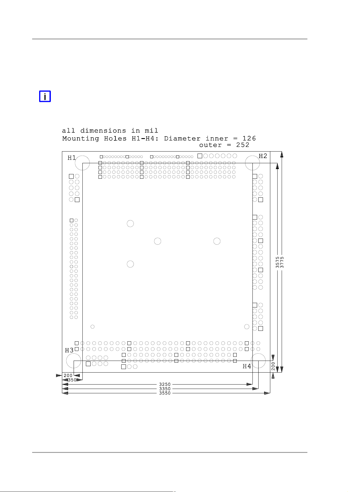
PCB: Mounting Holes Chapter: Mechanical Drawing
8 Mechanical Drawing
8.1 PCB: Mounting Holes
A true dimensioned drawing can be found in the PC/104 specification.
NOTE
All dimensions are in mil (1 mil = 0,0254 mm)
Beckhoff New Automation Technology CB4053 page 65
Page 66

Chapter: Mechanical Drawing PCB: Pin 1 Dimensions
8.2 PCB: Pin 1 Dimensions
NOTE
All dimensions are in mil (1 mil = 0,0254 mm)
page 66 Beckhoff New Automation Technology CB4053
Page 67

PCB: Heat Sink Chapter: Mechanical Drawing
8.3 PCB: Heat Sink
NOTE
All dimensions are in mil (1 mil = 0,0254 mm)
Beckhoff New Automation Technology CB4053 page 67
Page 68

Chapter: Technical Data Electrical Data
9 Technical Data
9.1 Electrical Data
Power Supply:
Board: 5 Volt +/- 5%
RTC: >= 3 Volt
Electric Power Consumption:
Board: tbd
RTC: <= 10µA
9.2 Environmental Conditions
Temperature Range:
Operating: 0°C to +60°C (extended temperature on request)
Storage: -25°C up to +85°C
Shipping: -25°C up to +85°C, for packaged boards
Temperature Changes:
Operating: 0.5°C per minute, 7.5°C per 30 minutes
Storage: 1.0°C per minute
Shipping: 1.0°C per minute, for packaged boards
Relative Humidity:
Operating: 5% up to 85% (non condensing)
Storage: 5% up to 95% (non condensing)
Shipping: 5% up to 100% (non condensing), for packaged boards
Shock:
Operating: 150m/s2, 6ms
Storage: 400m/s2, 6ms
Shipping: 400m/s2, 6ms, for packaged boards
Vibration:
Operating: 10 up to 58Hz, 0.075mm amplitude
58 up to 500Hz, 10m/s2
Storage: 5 up to 9Hz, 3.5mm amplitude
9 up to 500Hz, 10m/s2
Shipping: 5 up to 9Hz, 3.5mm amplitude
9 up to 500Hz, 10m/s2, for packaged boards
CAUTION
Shock and vibration figures pertain to the motherboard alone and do not include additional components
such as heat sinks, memory modules, cables etc.
page 68 Beckhoff New Automation Technology CB4053
Page 69

Thermal Specifications Chapter: Technical Data
9.3 Thermal Specifications
The board is specified to operate in an environmental temperature range from 0°C to +60°C (extended
temperature on request). Maximum die temperature is 90°C. To keep the processor under this threshold
an appropriate cooling solution needs to be applied. This solution has to take typical and maximum power
consumption into account. The maximum power consumption may be twice as high and should be used
as a basis for the cooling concept. Additional controllers may also affect the cooling concept. The power
consumption of such components may be comparable to the consumption of the processor.
The board design includes thermal solution mounting points that will provide the best possible thermal
interface between die and solution. Since we take thermal solutions seriously we have several advanced,
aggressive cooling solutions in our product portfolio. These solutions will support extended temperature
ranges in most environments in both active and passive varieties. Additionally, component underfill may
be necessary to reach extended temperature range limits. Please contact your sales representative to
order or discuss your thermal solution needs.
CAUTION
The end customer has the responsibility to ensure that the die temperature of the processor does not
exceed 90°C. Permanent overheating may destroy the board!
In case the temperature exceeds 90°C the environmental temperature must be reduced. Under certain
circumstances sufficient air circulation must be provided.
CAUTION
The CB4053 includes circuitry that will notify an intelligent power supply to shut down if the processor
reaches a critical temperature. This is achieved by deasserting the (low-active) PS_ON# signal found on
the SM-Bus connector. When PS_ON# is no longer pulled low, an intelligent power supply would take this
as a signal to shut down power. For this to work, PS_ON# must be connected to the power supply's
PS_ON input. If PS_ON# is not otherwise connected, the CB4053 can be damaged beyond repair if a
thermal shutdown event occurs. In rare instances, if power is not shut down, the board will continue to
heat up until failure occurs.
Beckhoff New Automation Technology CB4053 page 69
Page 70

Chapter: Support and Service Beckhoff's Branch Offices and Representatives
10 Support and Service
Beckhoff and their partners around the world offer comprehensive support and service, making available
fast and competent assistance with all questions related to Beckhoff products and system solutions.
10.1 Beckhoff's Branch Offices and Representatives
Please contact your Beckhoff branch office or representative for local support and service on Beckhoff
products.
The addresses of Beckhoff's branch offices and representatives around the world can be found on her
internet pages: http://www.beckhoff.com
You will also find further documentation for Beckhoff components there.
10.2 Beckhoff Headquarters
Beckhoff Automation GmbH
Eiserstr. 5
33415 Verl
Germany
phone: +49(0)5246/963-0
fax: +49(0)5246/963-198
e-mail: info@beckhoff.com
web: www.beckhoff.com
10.2.1 Beckhoff Support
Support offers you comprehensive technical assistance, helping you not only with the application of
individual Beckhoff products, but also with other, wide-ranging services:
o support
o design, programming and commissioning of complex automation systems
o and extensive training programs for Beckhoff system components
hotline: +49(0)5246/963-157
fax: +49(0)5246/963-9157
e-mail: support@beckhoff.com
10.2.2 Beckhoff Service
The Beckhoff Service Center supports you in all matters of after-sales service:
o on-site service
o repair service
o spare parts service
o hotline service
hotline: +49(0)5246/963-460
fax: +49(0)5246/963-479
e-mail: service@beckhoff.com
page 70 Beckhoff New Automation Technology CB4053
Page 71

Annex: Post-Codes
type and loading of the suitable Read/Write program into the run
I Annex: Post-Codes
Code Description
01h The Xgroup-program code is written in the random access memory from address 1000:0
onwards.
03h Initialise Variable/Routine "Superio_Early_Init".
05h 1. Cancel display
2. Cancel CMOS error flag
07h 1. Cancel 8042 (keyboard controller) Interface Register
2. Initialising and self testing of 8042 (keyboard controller)
08h 1. Test of special keyboard controllers (Winbond 977 super I/O Chip-series).
2. Enabling of the keyboard-interface register
0Ah 1. Disabling of the PS/2 mouse interface (optional).
2. Auto-detection of the connectors for Keyboard and mouse, optional: swap of PS/2 mouse
ports and PS/2 interfaces.
0Eh Test of the F000h-memory segment (Read/Write ability). In case of an error a signal will come
out of the loud speakers.
10h Auto-detection of the flash-rom-
time memory segment F000 (it is required for ESCD-data & the DMI-pool-support).
12h Interface-test of the CMOS RAM-logic (walking 1’s”-algorithm). Setting of the power status of
the real-time-clock (RTC), afterwards test of register overflow.
14h Initialising of the chip-set with default values. They can be modified through a software
(MODBIN) by the OEM-customer.
16h Initialise Variable/Routine "Early_Init_Onboard_Generator".
18h CPU auto-detection (manufacturer, SMI type (Cyrix or Intel), CPU-class (586 or 686).
1Bh Initialising if the interrupt pointer table. If nothing else is pretended, the hardware interrupts will
point on “SPURIOUS_INT_HDLR and the software interrupts will point on
SPURIOUS_soft_HDLR.
1Dh Initialise Variable/Routine EARLY_PM_INIT.
1Fh Load the keyboard table (Notebooks)
21h Initialising of the hardware power management (HPM) (Notebooks)
23h 1. Test the validity of the RTC-values (Example: “5Ah” is an invalid value for an RTC-minute).
2. Load the CMOS-values into the BIOS Stack. Default-values are loaded if CMOS-checksum
errors occur.
3. Preparing of the BIOS ‘resource map’ for the PCI & plug and play configuration. If ESCD is
valid, take into consideration the ESCD’s legacy information.
4. Initialise the onboard clock generator. Clock circuit at non-used PCI- and DIMM slots.
5. First initialising of PCI-devices: assign PCI-bus numbers - alot memory- & I/O resources -
search for functional VGA-controllers and VGA-BIOS and copy the latter into memory segment
C000:0 (Video ROM Shadow).
27h Initialise cache memory for INT 09
29h 1. Program the CPU (internal MTRR at P6 and PII) for the first memory address range (0-640K).
2. Initialising of the APIC at CPUs of the Pentium-class.
3. Program the chip-set according to the settings of the CMOS-set-up (Example: Onboard
IDE-controller).
4. Measuring of the CPU clock speed.
5. Initialise the video BIOS.
2Dh 1. Initialise the “Multi-Language”-function of the BIOS
2. Soft copy, e.g. Award-Logo, CPU-type and CPU clock speed…
33h Keyboard-reset (except super I/O chips of the Winbond 977 series)
3Ch Test the 8254 (timer device)
3Eh Test the interrupt Mask bits of IRQ-channel 1 of the interrupt controller 8259.
40h Test the interrupt Mask bits of IRQ-channel 2 of the interrupt controller 8259
43h Testing the function of the interrupt controller (8259).
47h Initialise EISA slot (if existent).
Beckhoff New Automation Technology CB4053 page 71
Page 72

Annex: Post-Codes
Code Description
49h 1. Determination of the entire memory size by revising the last 32-Bit double word of each 64k
memory segment.
2. Program “write allocation” at AMD K5-CPUs.
4Eh 1. Program MTRR at M1 CPUs
2. Initialise level 2-cache at CPUs of the class P6 and set the “cacheable range” of the random
access memory.
3. Initialise APIC at CPUs of the class P6.
4. Only for multiprocessor systems (MP platform): Setting of the “cacheable range” on the
respective smallest value (for the case of non-identical values).
50h Initialise USB interface
52h Testing of the entire random access memory and deleting of the extended memory (put on “0”)
55h Only for multi processor systems (MP platform): Indicate the number of CPUs.
57h 1. Indicate the plug and play logo
2. First ISA plug and play initialising – CSN-assignment for each identified ISA plug and play
device.
59h Initialise TrendMicro anti virus program code.
5Bh (Optional:) Indication of the possibility to start AWDFLASH.EXE (Flash ROM programming)
from the hard disk.
5Dh 1. Initialise Variable/Routine Init_Onboard_Super_IO.
2. Initialise Variable/Routine Init_Onbaord_AUDIO.
60h Release for starting the CMOS set-up (this means that before this step of POST, users are not
able to access the BIOS set-up).
65h Initialising of the PS/2 mouse.
67h Information concerning the size of random access memory for function call (INT 15h with
AX-Reg. = E820h).
69h Enable level 2 cache
6Bh Programming of the chip set register according to the BIOS set-up and auto-detection table.
6Dh 1. Assignment of resources for all ISA plug and play devices.
2. Assignment of the port address for onboard COM-ports (only if an automatic junction has
been defined in the setup).
6Fh 1. Initialising of the floppy controller
2. Programming of all relevant registers and variables (floppy and floppy controller).
73h Optional feature:
Call of AWDFLASH.EXE if:
- the AWDFLASH program was found on a disk in the floppy drive.
- the shortcut ALT+F2 was pressed.
75h Detection and installation of the IDE drives: HDD, LS120, ZIP, CDROM…
77h Detection of parallel and serial ports.
7Ah Co-processor is detected and enabled.
7Fh 1. Switch over to the text mode, the logo output is supported.
- Indication of possibly emerged errors. Waiting for keyboard entry.
- No errors emerged, respective F1 key was pressed (continue):
Deleting of the EPA- or own logo.
82h 1. Call the pointer to the “chip set power management”.
2. Load the text font of the EPA-logo (not if a complete picture is displayed)
3. If a password is set, it is asked here.
83h Saving of the data in the stack, back to CMOS.
84h Initialising of ISA plug and play boot drives (also Boot-ROMs)
85h 1. Final initialising of the USB-host.
2. At network PCs (Boot-ROM): Construction of a SYSID structure table
3. Backspace the scope presentation into the text mode
4. Initialise the ACPI table (top of memory).
5. Initialise and link ROMs on ISA cards
6. Assignment of PCI-IRQs
7. Initialising of the advanced power management (APM)
8. Set back the IRQ-register.
page 72 Beckhoff New Automation Technology CB4053
Page 73

Annex: Post-Codes
Code Description
93h Reading in of the hard disk boot sector for the inspection through the internal anti virus program
(trend anti virus code)
94h 1. Enabling of level 2 cache
2. Setting of the clock speed during the boot process
3. Final initialising of the chip set.
4. Final initialising of the power management.
5. Erase the onscreen and display the overview table (rectangular box).
6. Program “write allocation” at K6 CPUs (AMD)
7. Program “write combining” at P6 CPUs (INTEL)
95h 1. Program the changeover of summer-and winter-time
2. Update settings of keyboard-LED and keyboard repeat rates
96h 1. Multi processor system: generate MP-table
2. Generate and update ESCD-table
3. Correct century settings in the CMOS (20xx or 19xx)
4. Synchronise the DOS-system timer with CMOS-time
5. Generate an MSIRQ-Routing table..
C0h Chip set initialising:
- Cut off shadow RAM
- Cut off L2 cache (apron 7 or older)
- Initialise chip set register
C1h Memory detection:
Auto detection of DRAM size, type and error correction (ECC or none)
Auto detection of L2 cache size (apron 7 or older)
C3h Unpacking of the packed BIOS program codes into the random access memory.
C5h Copying of the BIOS program code into the shadow RAM (segments E000 & F000) via chipset
hook.
CFh Testing of the CMOS read/write functionality
FFh Boot trial over boot-loader-routine (software-interrupt INT 19h)
Beckhoff New Automation Technology CB4053 page 73
Page 74

Annex: Resources
II Annex: Resources
A IO Range
The used resources depend on setup settings.
The given values are ranges, which are fixed by AT compatibility. Other IO ranges are used, which are
dynamically adjusted by Plug & Play BIOS while booting.
Address Function
0-FF Reserved IO area of the board
170-17F
1F0-1F7 IDE1
278-27F
2E8-2EF
2F8-2FF COM2
370-377
378-37F LPT1
3BC-3BF
3E8-3EF
3F0-3F7
3F8-3FF COM1
B Memory Range
The used resources depend on setup settings.
If the entire range is clogged through option ROMs, these functions do not work anymore.
Address Function
A0000-BFFFF VGA RAM
C0000-CFFFF VGA BIOS
D0000-DFFFF AHCI BIOS / RAID / PXE (if available)
E0000-EFFFF System BIOS while booting
F0000-FFFFF System BIOS
C Interrupt
The used resources depend on setup settings.
The listed interrupts and their use are given through AT compatibility.
If interrupts must exclusively be available on the ISA side, they have to be reserved through the BIOS
setup. The exclusivity is not given and not possible on the PCI side.
Address Function
IRQ0 Timer
IRQ1 PS/2 Keyboard
IRQ2 (9)
IRQ3 COM1
IRQ4 COM2
IRQ5
IRQ6
IRQ7 LPT1
IRQ8 RTC
IRQ9
IRQ10
IRQ11
page 74 Beckhoff New Automation Technology CB4053
Page 75

Annex: Resources
Address Function
IRQ12 PS/2 Mouse
IRQ13 FPU
IRQ14 IDE Primary
IRQ15
D PCI Devices
All listed PCI devices exist on the board. Some PCI devices or functions of devices may be disabled in
the BIOS setup. Once a device is disabled other devices may get PCI bus numbers different from the
ones listed in the table.
AD INTA REQ Bus Dev. Fct. Controller / Slot
- - 0 0 0 Host Bridge ID8100h
A - 0 2 0 VGA Graphics ID8108h
A - 0 26 0 USB Client ID8118h
A - 0 27 0 HDA Controller ID811Bh
A - 0 28 0 PCI Express Port 1 ID8110h
B - 0 28 1 PCI Express Port 2 ID8112h
A - 0 29 0 USB UHCI Controller #1 ID8114h
B - 0 29 1 USB UHCI Controller #2 ID8115h
C - 0 29 2 USB UHCI Controller #3 ID8116h
D - 0 29 7 USB 2.0 EHCI Controller ID8117h
- - 0 30 0 SDIO/MMC Port 0
- - 0 30 1 SDIO/MMC Port 1
- - 0 30 2 SDIO/MMC Port 2
- - 0 31 0 LPC Interface ID8119h
- - 0 31 1 IDE Controller ID811Ah
A - (1) 0 0 LAN ID10D3h
- (2) 0 0 PCI Bridge IDE110h
20 A 0 (3) 4 External Slot 1
21 B 1 (3) 5 External Slot 2
22 C 2 (3) 6 External Slot 3
23 D 3 (3) 7 External Slot 4
E SMB Devices
The following table contains all reserved SM-Bus device addresses in 8-bit notation. Note that external
devices must not use any of these addresses even if the component mentioned in the table is not present
on the motherboard.
Address Function
10-11 Standard slave address
40-41 GPIO
60-61 BIOS internal
70-73 POST code output
88-89 BIOS-defined slave address
A0-A1 DIMM 1
A2-A3 DIMM 2
A4-AF BIOS internal
B0-BF BIOS internal
D2-D3 Clock
Beckhoff New Automation Technology CB4053 page 75
 Loading...