

Page 1
INSTRUCTION MANUAL
FOR
OVERCURRENT PROTECTION SYSTEM
BE1-851
MODBUS™ PROTOCOL
P0037-40
05-19-06
Publication: 9289900992
Revision: F 02/08
Page 2

Page 3

INTRODUCTION
This instruction manual provides detailed information about the BE1-851 Overcurrent Protection System
with the Modbus™ Protocol.
9289900992 Rev F BE1-851 Modbus™ Protocol i
Page 4

First Printing: May 1997
Printed in USA
© 2008 Basler Electric, Highland Illinois 62249 USA
All Rights Reserved
February 2008
CONFIDENTIAL INFORMATION
of Basler Electric, Highland Illinois, USA. It is loaned for confidential use, subject
to return on request, and with the mutual understanding that it will not be used in
any manner detrimental to the interest of Basler Electric.
It is not the intention of this manual to cover all details and variations in equipment, nor does this manual
provide data for every possible contingency regarding installation or operation. The availability and design
of all features and options are subject to modification without notice. Should further information be
required, contact Basler Electric.
BASLER ELECTRIC
ROUTE 143, BOX 269
HIGHLAND IL 62249 USA
http://www.basler.com, info@basler.com
PHONE +1 618.654.2341 FAX +1 618.654.2351
ii BE1-851 Modbus™ Protocol 9289900992 Rev F
Page 5

REVISION HISTORY
The following information provides a historical summary of the changes made to this instruction manual
(9289900992). Revisions are listed in reverse chronological order.
Manual
Revision and Date
F, 02/08
E, 12/06
D, 09/02
C, 03/01
B, 10/99
A, 06/99
—, 05/97
• Added information for style option 1, V and W.
• Updated ASCII Command Versus Modbus™ Register Cross
Reference.
• Added sensing input type “G” options.
• Added manual part number and revision to footers.
• Corrected pagination error occurring at page 30.
• Corrected table of contents margins.
• Corrected heading level 2 alignments.
• Changed the format of the manual to current standards and other
Modbus™ manuals.
• Corrected Floating Point Data Format on page 7.
• Added conventions on Password Security on pages 13 and 14.
• Added register 40989 on page 17.
• Expanded Notes on registers 40001 to 40006.
• Corrected the value of # for Report Focus in the table on page 35.
• Inserted paragraph under Global Parameters on page 36.
• Added register 40989 to Serial Port Setting Parameters on page 42.
• Corrected minor errors in the manual and SN registers 43498 to
43900 ordering.
• Added new registers 41110 to 41133 (Breaker Block Logic Mask),
41118 to 41121 (Breaker Block Logic Term), 41269 to 41270 (Logic
Alarm Mask), 41403 to 41406 (Reset Target Logic Mask), 41411 to
41414 (Reset Target Logic Term), 41419 to 41422 (Reset Alarm
Logic Mask), 41427 to 41430 (Reset Alarm Logic Term), and 47486
(Reset Logic Alarm Information).
• Updated register 40039 to support report #2 RA-LGC report.
• Added the Modbus™ Write support registers.
• Initial release.
Change
9289900992 Rev F BE1-851 Modbus™ Protocol iii
Page 6

This page intentionally left blank.
iv BE1-851 Modbus™ Protocol 9289900992 Rev F
Page 7

CONTENTS
SECTION 1 • GENERAL INFORMATION ................................................................................................ 1-1
SECTION 2 • REGISTER TABLE............................................................................................................. 2-1
SECTION 3 • REGISTER DETAILS ......................................................................................................... 3-1
SECTION 4 • ASCII CROSS REFERENCE ............................................................................................. 4-1
9289900992 Rev F BE1-851 Modbus™ Protocol v
Page 8

This page intentionally left blank.
vi BE1-851 Modbus™ Protocol 9289900992 Rev F
Page 9

SECTION 1 • GENERAL INFORMATION
INTRODUCTION
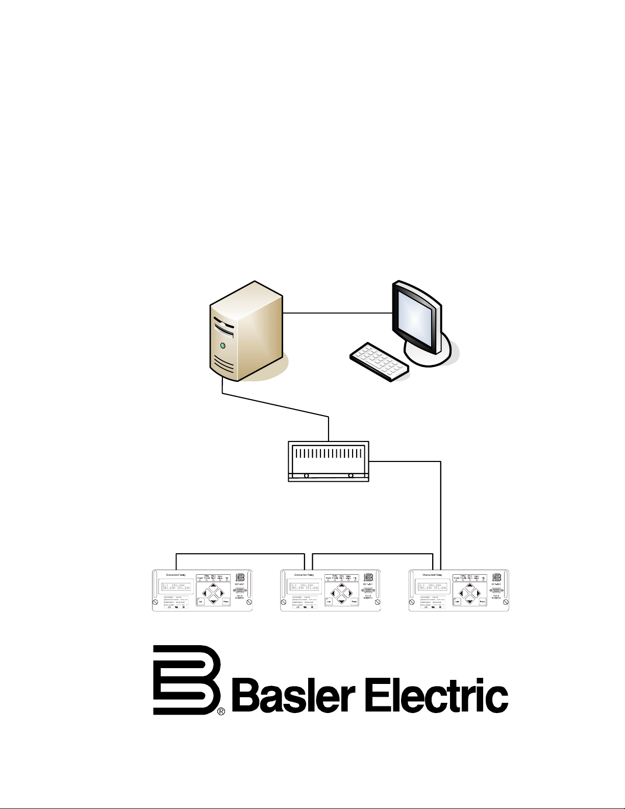
This document describes the Modbus™ communications protocol employed by BE1-851 relays and how
to exchange information with BE1-851 relays over a Modbus™ network. The BE1-851 communicates by
emulating a subset of the Modicon 984 Programmable Controller.
FUNCTIONAL DESCRIPTION
Modbus™ communications use a master-slave technique in which only the master can initiate a
transaction. This transaction is called a query. When appropriate, a slave (BE1-851) responds to the
query. When a Modbus™ master communicates with a slave, information is provided or requested by the
master. Information residing in the BE1-851 is grouped categorically as follows:
• Session Parameters
• Global Parameters
• Control Parameters (Select Before Operate)
• Setting Parameters
• Report Parameters
• Metering Parameters
All supported data can be read as specified in the register table. Abbreviations are used in the Register
Table to indicate the register type. Register types are:
• Read/Write = RW
• Read Only = R -
Select Before Operate (SBO) functions are used to change active settings groups and control outputs.
There are two settings groups in the BE1-851, one of which may be selected as active using SBO
commands.
When a slave receives a query, the slave responds by either supplying the requested data to the master
or performing the requested action. A slave device never initiates communications on the Modbus™ and
will always generate a response to the query unless certain error conditions occur. The BE1-851 is
designed to communicate on the Modbus™ only as a slave device.
A master can query slaves individually or universally. A universal (“broadcast”) query, when allowed,
evokes no response from any slave device. If a query to an individual slave device requests actions
unable to be performed by the slave, the slave response message contains an exception response code
defining the error detected. Exception response codes are quite often enhanced by the information found
in the “Error Details” block of holding registers.
Message Structure
Master initiated queries and BE1-851 responses share the same message structure. Each message is
comprised of four message fields. They are:
• Device Address (1 byte)
• Function Code (1 byte)
• Data Block (n bytes)
• Error Check field (2 bytes)
Device Address Field
The device address field contains the unique Modbus™ address of the slave being queried. The
addressed slave repeats the address in the device address field of the response message. This field is 1
byte.
Although Modbus™ protocol limits a device address from 1 - 247, a BE1-851 can be assigned a device
address in the range of 1 - 65534. The address is user-selectable at installation and can be altered during
real-time operation.
9289900992 Rev F BE1-851 Modbus™ Protocol 1-1
Page 10

Function Code Field
The function code field in the query message defines the action to be taken by the addressed slave. This
field is echoed in the response message and is altered by setting the most significant bit (MSB) of the
field to 1 if the response is an error response. This field is 1 byte.
The BE1-851 maps all available data into the Modicon 984 holding register address space (4XXXX) and
supports the following function codes:
• Function 03 (03 hex) - read holding registers
• Function 06 (06 hex) - preset single register (write single holding register)
• Function 08 (08 hex), subfunction 00 - diagnostics: return query data
• Function 08 (08 hex), subfunction 01 - diagnostics: restart communications option
• Function 08 (08 hex), subfunction 04 - diagnostics: force listen only mode
• Function 16 (10 hex) - preset multiple registers, non-broadcast and broadcast
Data Block Field
The query data block contains additional information needed by the slave to perform the requested
function. The response data block contains data collected by the slave for the queried function. An error
response will substitute an exception response code for the data block. The length of this field varies with
each query. See the paragraphs on Register Definitions in this manual for interpretation of data.
Error Check Field
The error check field provides a method for the slave to validate the integrity of the query message
contents and allows the master to confirm the validity of response message contents. This field is 2 bytes.
Serial Transmission Details
A standard Modbus™ network offers two transmission modes for communication: ASCII or remote
terminal unit (RTU). The BE1-851 supports only the RTU mode.
Each 8-bit byte in a message contains two 4-bit hexadecimal characters. The message is transmitted in a
continuous stream with the LSB of each byte of data transmitted first. Transmission of each 8-bit data
byte occurs with one start bit and either one or two stop bits. Parity checking is performed, when enabled,
and can be either odd or even. The transmission baud rate is user-selectable and can be set at
installation and altered during real-time operation. The BE1-851 Modbus™ supported baud rates are
2400, 4800, 9600, and 19200. The factory default baud rate is 9600.
BE1-851 supports both RS-232-C and RS-485 compatible serial interfaces. Both interfaces are
accessible from the rear panel of the BE1-851. The RS-232-C interfaces (front and rear) are configured
for ASCII command mode while the RS-485 interface is configured for Modbus™ communication when
this option is installed. The eighth character of the relay style number must be “1” for the relay to be
configured for Modbus™.
Message Framing and Timing Considerations
When receiving a message, the BE1-851 requires an inter-byte latency of 3.5 character times before
considering the message complete.
Once a valid query is received, the BE1-851 waits a specified amount of time before responding. This
time delay is set in the remote delay time parameter with the SG-COM ASCII command. This parameter
contains a value from 10 - 200 milliseconds. The default value is 10 milliseconds.
Table 1-1 provides the response message transmission time (in seconds) and 3.5 character times (in
milliseconds) for various message lengths and baud rates.
Table 1-1. Timing Considerations
Baud Rate 3.5 Character Time (mSec)
Message Tx Time (seconds)
128 Bytes 256 Bytes
2400 16.04 0.59 1.17
4800 8.021 0.29 0.59
9600 4.0104 0.15 0.29
19200 2.0052 0.07 0.15
1-2 BE1-851 Modbus™ Protocol 9289900992 Rev F
Page 11
Error Handling and Exception Responses
Any query received that contains a non-existent device address, a framing error, or CRC error is ignored.
No response is transmitted. Queries addressed to a BE1-851 with an unsupported function or illegal
values in the data block result in an error response message with an exception response code. The
exception response codes supported by the BE1-851 are provided in Table 1-2.
Table 1-2. Supported Exception Response Codes
Code Name Meaning
01 Illegal Function
02 Illegal Data Address
03 Illegal Data Value
The query Function/Subfunction Code is unsupported; query read
of more than 125 registers; query preset of more than 100 registers
A register referenced in the data block does not support queried
read/write; query preset of a subset of a numerical register group.
A preset register data block contains an incorrect number of bytes
or one or more data values out of range.
COMMUNICATIONS HARDWARE REQUIREMENTS
The BE1-851 RS-485 physical interface is three positions of a terminal strip with locations for
Send/Receive A (A), Send/Receive B (B), and Signal Ground (C). Refer to the BE1-851 Instruction
Manual (9289900990) for further details.
DETAILED MESSAGE QUERY AND RESPONSE
A detailed description of BE1-851 supported message queries and responses is provided in the following
paragraphs.
Read Holding Registers
Query
This query message requests a register or block of registers to be read. The data block contains the
starting register address and the quantity of registers to be read. A register address of N will read holding
register N+1. If the query is a broadcast (device address = 0), no response message is returned.
Device Address
Function Code = 03 (hex)
Starting Address Hi
Starting Address Lo
No. of Registers Hi
No. of Registers Lo
CRC Hi error check
CRC Lo error check
The number of registers cannot exceed 125 without causing an error response with the exception code
for an illegal function.
Response
The response message contains the data queried. The data block contains the block length in bytes
followed by the data (one Data Hi byte and one Data Lo byte) for each requested register.
Reading an unassigned holding register returns a value of zero.
Device Address
Function Code = 03 (hex)
Byte Count
Data Hi (For each requested register, there is one Data Hi and one Data Lo.)
9289900992 Rev F BE1-851 Modbus™ Protocol 1-3
Page 12

Data Lo
Data Hi
Data Lo
CRC Hi error check
CRC Lo error check
Return Query Data
This query contains data to be returned (looped back) in the response. The response and query
messages should be identical. If the query is a broadcast (device address = 0), no response message is
returned.
Device Address
Function Code = 08 (hex)
Subfunction Hi = 00 (hex)
Subfunction Lo = 00 (hex)
Data Hi = xx (don't care)
Data Lo = xx (don't care)
CRC Hi error check
CRC Lo error check
Restart Communications Option
This query causes the remote communications function of the BE1-851 to restart, terminating an active
listen only mode of operation. No effect is made upon primary relay operations. Only the remote
communications function is affected. If the query is a broadcast (device address = 0), no response
message is returned.
If the BE1-851 receives this query while in the listen only mode, no response message is generated.
Otherwise, a response message identical to the query message is transmitted prior to the
communications restart.
Device Address
Function Code = 08 (hex )
Subfunction Hi = 00 (hex)
Subfunction Lo = 01 (hex)
Data Hi = xx (don't care)
Data Lo = xx (don't care)
CRC Hi error check
CRC Lo error check
Listen Only Mode
This query forces the addressed BE1-851 to the listen only mode for Modbus™ communications, isolating
it from other devices on the network. No responses are returned.
While in the Listen Only mode, the BE1-851 continues to monitor all queries. The BE1-851 does not
respond to any other query until the listen only mode is removed. All write requests with a query to Preset
Multiple Registers (Function Code = 16) are also ignored. When the BE1-851 receives the restart
communications query, the Listen Only mode is removed.
Device Address
Function Code = 08 (hex)
Subfunction Hi = 00 (hex)
Subfunction Lo = 04 (hex)
Data Hi = xx (don't care)
Data Lo = xx (don't care)
CRC Hi error check
CRC Lo error check
1-4 BE1-851 Modbus™ Protocol 9289900992 Rev F
Page 13

Preset Multiple Registers
A preset multiple registers query could address multiple registers in one slave or multiple slaves. If the
query is a broadcast (device address = 0), no response message is returned.
Query
A Preset Multiple Register query message requests a register or block of registers to be written. The data
block contains the starting address and the quantity of registers to be written, followed by the Data Block
byte count and data. The BE1-851 will perform the write when the device address is the same as the
BE1-851 remote address or when the device address is 0. A device address is 0 for a broadcast query.
A register address of N will write Holding Register N+1.
Data will cease to be written if any of the following exceptions occur:
• Queries to write to Read only registers result in an error response with Exception Code of “Illegal
Data Address.”
• Queries attempting to write more than 100 registers cause an error response with Exception
Code “Illegal Function.”
• An incorrect Byte Count will result in an error response with Exception Code of “Illegal Data
Value.”
• There are several instances of registers that are grouped together to collectively represent a
single numerical BE1-851 data value (i.e., floating point data and 32-bit integer data). A query to
write a subset of such a register group will result in an error response with Exception Code “Illegal
Data Address.”
• A query to write a not allowed value (out of range) to a register results in an error response with
Exception Code of “Illegal Data Value.”
Device Address
Function Code = 10 (hex)
Starting Address Hi
Starting Address Lo
No. of Registers Hi
No. of Registers Lo
Byte Count
Data Hi
Data Lo
.
.
Data Hi
Data Lo
CRC Hi error check
CRC Lo error check
Response
The response message echoes the starting address and the number of registers. There is no response
message when the query is a broadcast (device address = 0).
Device Address
Function Code = 10 (hex)
Starting Address Hi
Starting Address Lo
No. of Registers Hi
No. of Registers Lo
CRC Hi Error Check
CRC Lo Error Check
Preset Single Register (Write Single Holding Register)
A Preset Single Register query message requests a single register to be written. The BE1-851 will
perform the write when the device address is the same as the BE1-851 remote address.
9289900992 Rev F BE1-851 Modbus™ Protocol 1-5
Page 14

Query
Data will cease to be written if any of the following exceptions occur:
• Queries to write to Read only registers result in an error response with Exception Code of “Illegal
Data Address.”
• A query to write a value that is not allowed (out of range) to a register results in an error response
with Exception Code of “Illegal Data Value.”
Device Address
Function Code = 06 (hex )
Address Hi
Address Lo
Data Hi
Data Lo
CRC Hi error check
CRC Lo error check
Response
The response message echoes the Query message after the register has been altered.
DATA FORMATS
BE1-851 data varies from one to four bytes in length. Single byte data resides in the holding register
least-significant byte with the most-significant byte set to zero. Floating-point data and long integer data
(each 32-bits in length) place the two most-significant bytes in the higher holding register address of the
associated register pair.
Floating Point Data Format (FP)
The Modbus™ floating point data format uses two consecutive holding registers to represent a data value.
The first register contains the low-order 16 bits of the following 32-bit format:
• MSB is the sign bit for the floating-point value (0 = positive).
• The next 8 bits are the exponent biased by 127 decimal.
• The 23 LSBs comprise the normalized mantissa. The most-significant bit of the mantissa is always
assumed to be 1 and is not explicitly stored, yielding an effective precision of 24 bits.
The value of the floating-point number is obtained by multiplying the binary mantissa times two raised to
the power of the unbiased exponent. The assumed bit of the binary mantissa has the value of 1.0, with
the remaining 23 bits providing a fractional value. Table 1-3 shows the floating-point format.
Table 1-3. Floating Point Format
Sign Exponent + 127 Mantissa
1 bit 8 bits 23 bits
The floating-point format allows for values ranging from approximately 8.43X10
point value of all zeroes is the value zero. A floating-point value of all ones (not a number) signifies a
value currently not applicable or disabled.
Example
will read from two consecutive holding registers as follows:
: The value 95,800 represented in floating point format is hexadecimal 47BB1C00. This number
-37
to 3.38X1038. A floating-
Holding Register
K (Hi Byte) hex 1C
K (Lo Byte) hex 00
K+1 (Hi Byte) hex 47
K+1 (Lo Byte) hex BB
The same byte alignments are required to write.
1-6 BE1-851 Modbus™ Protocol 9289900992 Rev F
Value
Page 15

Double Precision Data Format (DP)
The legacy version of BE1-851 Modbus™ supports the double precision data format, which uses two
consecutive registers to represent a data value. The first register (A) contains the high-order 16 bits of
double precision data, and is the actual data value divided by 10,000.
The second register (B) contains the low-order 16 bits of double precision data, and is the actual data
∗
value plus 10,000. The format is: Double Precision = (A
Example
hexadecimal 000916A8. This number will read from two consecutive holding registers as follows:
Holding Register
K (Hi Byte) hex 00
K (Lo Byte) hex 09
K+1 (Hi Byte) hex 16
K+1 (Lo Byte) hex A8
The same byte alignments are required to write.
Long Integer Data Format (LI)
The Modbus™ long integer data format uses two consecutive holding registers to represent a 32-bit data
value. The first register contains the low-order 16 bits and the second register contains the high-order 16
bits.
Example
will read from two consecutive holding registers as follows:
Holding Register
K (Hi Byte) hex 76
K (Lo Byte) hex 38
K+1 (Hi Byte) hex 00
K+1 (Lo Byte) hex 01
The same byte alignments are required to write.
: The value 95,800 represented in double precision format is: 95800 = (9 ∗ 10,000) + 5,800, or
Value
: The value 95,800 represented in long integer format is hex adecimal 0x00017638. This number
Value
10,000) + B.
Integer Data Format (INT)
The Modbus™ integer data format uses a single holding register to represent a 16-bit data value.
Example
from a holding register as follows:
Holding Register
K (Hi Byte) hex 12
K (Lo Byte) hex 34
The same byte alignments are required to write.
Short Integer Data Format (SI)
The Modbus™ short integer data format uses a single holding register to represent an 8 bit data value.
The holding register high byte will always be zero.
Example
from a holding register as follows:
Holding Register
K (Hi Byte) hex 00
K (Lo Byte) hex 84
The same byte alignments are required to write.
9289900992 Rev F BE1-851 Modbus™ Protocol 1-7
: The value 4660 represented in integer format is hexadecimal 0x1234. This number will read
Value
: The value 132 represented in short integer format is hexadecimal 0x84. This number will read
Value
Page 16

ASCII Character Data Format (ASC (1))
The Modbus™ ASCII character data format uses a single holding register to represent a single character
value. The holding register high byte will always be zero with the ASCII character code in the low byte.
Example
: The character ‘D’ represented in ASCII character format is hexadecimal 44. This number will
read from a holding register as follows:
Holding Register
Value
K (Hi Byte) hex 00
K (Lo Byte) hex 44
The same byte alignments are required to write.
ASCII String Data Format (ASC (x))
The Modbus™ ASCII string data format uses one or more holding registers to represent a sequence or
string, of character values. If the string contains a single character, the holding register high byte will
contain the ASCII character code and the low byte will be zero.
Example
: The string “PASSWORD” represented in ASCII string format will read as follows:
Holding Register
Value
K (Hi Byte) ‘P’
K (Lo Byte) ‘A’
K+1 (Hi Byte) ‘S’
K+1 (Lo Byte) ‘S’
K+2 (Hi Byte) ‘W’
K+2 (Lo Byte) ‘O’
K+3 (Hi Byte) ‘R’
K+3 (Lo Byte) ‘D’
Example
: If the above string is changed to “P,” the new string will read as follows:
Holding Register
Value
K (Hi Byte) ‘P’
K (Lo Byte) hex 00
K+1 (Hi Byte) hex 00
K+1 (Lo Byte) hex 00
K+2 (Hi Byte) hex 00
K+2 (Lo Byte) hex 00
K+3 (Hi Byte) hex 00
K+3 (Lo Byte) hex 00
The same byte alignments are required to write.
Bit Mapped Data Format (BM (x))
The bit mapped data format uses two or more holding registers to represent a sequence of bit values.
The Modbus™ Bit Map data format can represent an 8 bit, 16 bit, 32 bit, or 64 bit value.
Example
: The Bit Map value of the hexadecimal number 0x123456789ABCDEF0 using a BM64 format
will read as follows:
Holding Register
Value
K (Hi Byte) 0x12
K (Lo Byte) 0x34
K+1 (Hi Byte) 0x56
K+1 (Lo Byte) 0x78
K+2 (Hi Byte) 0x9A
1-8 BE1-851 Modbus™ Protocol 9289900992 Rev F
Page 17

K+2 (Lo Byte) 0xBC
K+3 (Hi Byte) 0xDE
K+3 (Lo Byte) 0xF0
CRC Error Check
This field contains a two-byte CRC value for transmission error detection. The master first calculates the
CRC and appends it to the query message. The BE1-851 recalculates the CRC value for the received
query and performs a comparison to the query CRC value to determine if a transmission error has
occurred. If so, no response message is generated. If no transmission error has occurred, the slave
calculates a new CRC value for the response message and appends it to the message for transmission.
The CRC calculation is performed using all bytes of the device address, function code, and data block
fields. A 16-bit CRC-register is initialized to all 1's. Then each eight-bit byte of the message is used in the
following algorithm.
First, exclusive-OR the message byte with the low-order byte of the CRC-register. The result, stored in
the CRC-register, will then be right-shifted eight times. The CRC-register MSB is zero-filled with each
shift. After each shift, the CRC-register LSB is examined. If the LSB IS a 1, the CRC-register is then
exclusive-ORed with the fixed polynomial value A001 (hex) prior to the next shift. Once all bytes of the
message have undergone the above algorithm, the CRC-register will contain the message CRC value to
be placed in the error check field.
Session Access Registers
The ACCESS REQUEST and the EXIT registers are used to access and release write privileges while
changing relay settings, resetting report registers or using control commands through the Modbus™ port.
This feature is important because it prevents changes from being made concurrently from two areas. For
example, a user cannot make changes from COM 0 at the same time a remote user is making changes
via Modbus™ from COM 2.
Changing the settings through the Modbus™ port requires that the operator write to the ACCESS
REQUEST register to obtain programming access. This must follow writing the ACCESS PASSWORD
register(s) with a password to obtain access to change settings associated with the password. Different
passwords give the ability or access to perform different operations. The relay will deny access if an
invalid password is entered or if another user has already been granted programming access through
another serial port or at the front panel. Only one user can have access at any one time.
If no password protection is used, it is still necessary to obtain access in order to protect against
accidental changes. If password protection is disabled, then writing the ACCESS REQUEST register will
be accepted in place of a password. The relay will transmit a valid response message if the access query
was received and executed. The relay will respond with an error message if the access query could not
be executed.
Changing settings through a Modbus™ communication port consists of the following sequence:
1. Preset Multiple Registers query to ACCESS PASSWORD register(s) to specify password.
2. Preset Multiple Registers query to ACCESS REQUEST register to access write privileges.
3. Preset Multiple Registers queries to change the current settings.
4. Preset Multiple Registers query to EXIT register to clear access and save.
Changes are not made to the working settings but to a scratch-pad copy of the settings. After the
change(s) are made, the new data will be copied to the working settings and saved to non-volatile
memory when the EXIT register is written with a ‘Y.’ It is important to make all changes to relay
parameters before writing the EXIT register. This prevents a partial or incomplete protection scheme from
being implemented.
Template Registers
The BE1-851 uses three templates. A template is a block of holding registers to which the user assigns
one of a number of similar groups of parameters. Templates are used for settings groups, fault
summaries, and report generation. Modbus™ Template Registers 40036 (Settings Group Selection),
40038 (Fault Number Selection), 40039 (Report Selection), and 40040 (Report Focus) DO NOT
REQUIRE any Write Password Access level before they can be written to.
9289900992 Rev F BE1-851 Modbus™ Protocol 1-9
Page 18

The BE1-851 has four settings groups. The GRP temp late is assigned the parameters of a settings group.
Therefore, before reading or writing settings group values, a user must first specify which settings group is
to be associated with the template. This is accomplished by writing the desired settings group number (0 -
3) into the SETTINGS GROUP SELECTION Template holding register.
The BE1-851 can store up to 16 faults. Each fault is accessed by its fault number, which ranges from 1 to
255. The FLT template is assigned the parameters of a particular fault occurrence. Therefore, before
reading fault summary values, a user must first specify which fault number is to be associated with the
template. This is accomplished by writing the desired fault number (1 - 255) into the FAULT SELECTION
Template holding register.
The BE1-851 generates 10 ASCII reports. The RPT templa te is assigned the text of a report. Therefore,
before reading report text, a user must first specify which report is to be associated with the template. This
is accomplished by writing the desired report number into the REPORT SELECTION Template holding
register along with the associated report identifier, if any, into the REPORT FOCUS Template holding
register.
Fault Summary Registers
The user can enter any fault number (1 - 255) into the FAULT SELECTION Template holding register to
associate summary parameters for that fault number with the FLT Template. The Fault Template Status
register (47513) indicates whether that fault number specifies a recent fault (one of 16 stored faults). If so,
the Fault Template Status register value is the fault number; otherwise, it is zero and all FLT template
values will read zero.
The Fault Indicator register (47512) value is the fault number (1 - 255) of the most recent fault. The user
may construct his front-end GUI to link this register value into the FAULT SELECTION Template holding
register, thereby automatically associating the FLT template with the most recent fault occurrence.
Report Generation Registers
The BE1-851 generates numerous ASCII reports available via serial commands. Several of these reports
are available intact via the Modbus™ communication port. The desired report is first specified by writing
the REPORT SELECTION holding register. If the report requires a number to be specified, such as a fault
number or number of events, that number is written into the REPORT FOCUS holding register. The report
is then available via the RPT template. The report can be read from 1 to 125 registers at a time, with each
register containing 2 ASCII characters of information. The report read queries could be interspersed
among other query types. The RPT template is continually re-read until the report has completed. Once
the report is complete, reading from the RPT template will continually return the ASCII character code of
127 (“7F” hexadecimal). The report cannot be re-read or another report read until the REPORT
SELECTION holding register is re-written.
Contiguous Poll Block Registers
The user may allocate up to 125 holding registers to the Contiguous Poll Block (49875-999). This
allocation allows dispersed registers, which are frequently read to be polled via a single read query. A
register is assigned to a position in the Poll Block by writing its address value into the corresponding
position in the Contiguous Poll Block Assignments registers (40746-870). Writing a zero value leaves that
Poll Block position unassigned. Once assignments are made, the values of the assigned registers may be
read by polling the Contiguous Poll Block. Polling an unassigned position will return a value of zero.
For example, if you wanted to continuously monitor the Date (47364), Time (47365-66), Fault Indicator
(47512) and Breaker Status (47388) Holding Registers, you would first configure the Contiguous Poll
Block Registers by writing the desired register address values 7364, 7365, 7366, 7512 and 7388 into the
Contiguous Poll Block Assignment registers 40746 through 40750, respectively. You may now begin
monitoring the specified registers by reading the first 5 locations in the Contiguous Poll Block; i.e., reading
register 49875 for the Date (as specified in it’s corresponding assignment register 40746), reading
register 49876 and 77 for the Time (as specified in their corresponding assignment registers 40747 and
48), reading register 49878 for the Fault Indicator (as specified in it’s corresponding assignment register
40749) and reading register 49879 for the Breaker Status (as specified in it’s corresponding assignment
register 40750).
Exception Code Enhancement Registers
When a BE1-851 responds to a Preset Multiple Register query with an error response message,
additional information detailing the cause of the error may be available in the ERROR DETAILS block of
1-10 BE1-851 Modbus™ Protocol 9289900992 Rev F
Page 19

holding registers (49835-54). The information is in ASCII format and available by reading the message
string from the ERROR DETAILS block. The message remains available until the next Preset Multiple
Register query is executed unless that query is to the FAULT SELECTION Template holding register.
Since this register can be written automatically and randomly in time, the ERROR DETAILS block will not
be updated.
The ERROR DETAILS block will also contain the exit status following a Preset Multiple Register query to
the EXIT (40001) register. You may clear the ERROR DETAILS message at any time without affecting
system operation by sending a Preset Multiple Register query to any unassigned holding register.
9289900992 Rev F BE1-851 Modbus™ Protocol 1-11
Page 20

This page intentionally left blank.
1-12 BE1-851 Modbus™ Protocol 9289900992 Rev F
Page 21

SECTION 2 • REGISTER TABLE
MAPPING BE1-851 PARAMETERS INTO MODICON HOLDING REGISTER ADDRESS SPACE
General
Parameters are mapped into the holding register address space (40001 - 49999) in blocks according to
access type.
Any Holding Register not listed in the Register Table is an unassigned Holding Register. A value of zero
always results when reading an unassigned Holding Register. Writes to unassigned Holding Registers
are legal, but no action will be taken (the write is ignored).
Conventions
The Data Format column uses the following abbreviations:
ASC(x) - ASCII string, where x = the maximum defined string length
BM(x) - Bit-map, where x = the number of related bits
FP - Floating point
INT - Integer (16-bit integer)
LI - Long Integer (32-bit integer)
SI - Short Integer (8-bit integer)
DP - Double Precision (legacy BE1-851 only)
The Notes column uses the following abbreviations:
GRP - Group Template Member
FLT - Fault Template Member
RPT - Report Template Member
NS - Not Supported
TS - Time Stamp format: MSEC of the day (0 to 86,400,000 ms) and days since 01/01/1984.
LEG - Original (legacy) BE1-851 Modbus™ parameter mapping.
PS - Effective only when the Password Security parameter is enabled. See REGISTER DETAILS for
Password Security holding register 40989.
PW - Effective for any communication port active with ASCII protocol and for the Modbus™ port
(COM 2) when Password Security is enabled.
9289900992 Rev F BE1-851 Modbus™ Protocol 2-1
Page 22

RESISTER TABLE - ORDERED BY REGISTER NUMBER
Holding Read/Write Data Register Parameter Supported Format Notes
Session Parameters
40001 Exit R W ASC(1) PS
40002-05 Access Password R W ASC(8) PS
40006 Access Request R W BM(16) PS
Template Parameters
40036 Settings Group Selection R W SI
40038 Fault Selection R W SI
40039 Report Selection R W SI
40040 Report Focus R W INT
Global Parameters
40080-83 Global Password R W ASC(8) PW
40084 Global Path R W BM(8) PW
40085-88 Setting Password R W ASC(8) PW
40089 Setting Path R W BM(8) PW
40090-93 Control Password R W ASC(8) PW
40094 Control Path R W BM(8) PW
40095-98 Report Password R W ASC(8) PW
40099 Report Path R W BM(8) PW
Control Parameters
40117 Select Group R W ASC(1)
40118 Operate Group R W ASC(1)
40119 Select Virtual Selector Switch 43 R W ASC(1)
40120 Operate Virtual Selector Switch 43 R W ASC(1)
40121 Select Virtual Selector Switch 143 R W ASC(1)
40122 Operate Virtual Selector Switch 143 R W ASC(1)
40123 Select Virtual Selector Switch 243 ∗ R W ASC(1)
40124 Operate Virtual Selector Switch 243 ∗ R W ASC(1)
40125 Select Virtual Selector Switch 343 ∗ R W ASC(1)
40126 Operate Virtual Selector Switch 343 ∗ R W ASC(1)
40135 Select 101 Virtual Breaker Control Switch R W ASC(1)
40136 Operate 101 Virtual Breaker Control Switch R W ASC(1)
40137 Select All Outputs R W ASC(1)
40138 Operate All Outputs R W ASC(1)
40139 Select Output A R W ASC(1)
40140 Operate Output A R W ASC(1)
40141 Select Output 1 R W ASC(1)
40142 Operate Output 1 R W ASC(1)
40143 Select Output 2 R W ASC(1)
40144 Operate Output 2 R W ASC(1)
40145 Select Output 3 R W ASC(1)
40146 Operate Output 3 R W ASC(1)
2-2 BE1-851 Modbus™ Protocol 9289900992 Rev F
Page 23

Holding Read/Write Data Register Parameter Supported Format Notes
40147 Select Output 4 R W ASC(1)
40148 Operate Output 4 R W ASC(1)
40149 Select Output 5 R W ASC(1)
40150 Operate Output 5 R W ASC(1)
∗ 243 and 343 are not available when style option 1 is V or W.
Group Setting Parameters
40269-70 50TP Pickup R W FP GRP
40271-72 50TP Time Delay R W LI GRP
40273-74 50TN Pickup R W FP GRP
40275-76 50TN Time Delay R W LI GRP
40277-78 50TQ Pickup (250TN, Sensing input “G”) R W FP GRP
40279-80 50TQ Time Delay (250TN, Sensing input “G”) R W LI GRP
40281-82 150TP Pickup R W FP GRP
40283-84 150TP Time Delay R W LI GRP
40285-86 150TN Pickup R W FP GRP
40287-88 150TN Time Delay R W LI GRP
40289-90 150TQ Pickup (350TN, Sensing input “G”) R W FP GRP
40291-92 150TQ Time Delay (350TN, Sensing input “G”) R W LI GRP
40305-06 51P Pickup R W FP GRP
40307-08 51P Time Dial R W FP GRP
40309-10 51P Curve Type R W ASC(3) GRP
40311-12 51N Pickup R W FP GRP
40313-14 51N Time Dial R W FP GRP
40315-16 51N Curve Type R W ASC(3) GRP
40317-18 51Q Pickup (151N, Sensing input “G”) R W FP GRP
40319-20 51Q Time Dial (151N, Sensing input “G”) R W FP GRP
40321-22 51Q Curve Type (151N, Sensing input “G”) R W ASC(3) GRP
40359-60 62 Time Delay 1 R W LI GRP
40361-62 62 Time Delay 2 R W LI GRP
40363-64 162 Time Delay 1 R W LI GRP
40365-66 162 Time Delay 2 R W LI GRP
40367-68 262 Time Delay 1 ∗ R W LI GRP
40369-70 262 Time Delay 2 ∗ R W LI GRP
40371-72 362 Time Delay 1 ∗ R W LI GRP
40373-74 362 Time Delay 2 ∗ R W LI GRP
40406-07 79 First Automatic Reclose Delay R W LI GRP
40408-09 79 Second Automatic Reclose Delay R W LI GRP
40410-11 79 Third Automatic Reclose Delay R W LI GRP
40412-13 79 Fourth Automatic Reclose Delay R W LI GRP
40414-15 79 Reset Time Delay R W LI GRP
40416-17 79 Reclose Fail Time Delay R W LI GRP
40418-19 79 Maximum Reclose Time R W LI GRP
40420 79 Sequence Control R W BM(16) GRP
∗ 262 and 362 are available when style option 1 is V or W.
Global Setting Parameters
40606-07 Breaker Fail Time Delay R W LI
40608-09 Programmable 51 Curve Constant A R W FP
40610-11 Programmable 51 Curve Constant B R W FP
40612-13 Programmable 51 Curve Constant C R W FP
9289900992 Rev F BE1-851 Modbus™ Protocol 2-3
Page 24

Holding Read/Write Data Register Parameter Supported Format Notes
40614-15 Programmable 51 Curve Constant N R W FP
40616-17 Programmable 51 Curve Constant R R W FP
40618 Input 1 Contact Recognition Time Delay R W SI
40619 Input 1 Contact Debounce Time Delay R W SI
40620 Input 2 Contact Recognition Time Delay R W SI
40621 Input 2 Contact Debounce Time Delay R W SI
40622 Input 3 Contact Recognition Time Delay R W SI
40623 Input 3 Contact Debounce Time Delay R W SI
40624 Input 4 Contact Recognition Time Delay R W SI
40625 Input 4 Contact Debounce Time Delay R W SI
Contiguous Poll Block
40746-870 Contiguous Poll Block Assignments R W INT
Setting Group Control
40871 Setting Group Control On Time R W INT
40872 Setting Group 1 Automatic Control Switch Time R W SI
40873 Setting Group 1 Automatic Control Switch Level R W SI
40874 Setting Group 1 Automatic Control Return Time R W SI
40875 Setting Group 1 Automatic Control Return Level R W SI
40876 Setting Group 1 Tracking Element R W INT
40877 Setting Group 2 Automatic Control Switch Time R W SI
40878 Setting Group 2 Automatic Control Switch Level R W SI
40879 Setting Group 2 Automatic Control Return Time R W SI
40880 Setting Group 2 Automatic Control Return Level R W SI
40881 Setting Group 2 Tracking Element R W INT
40882 Setting Group 3 Automatic Control Switch Time R W SI
40883 Setting Group 3 Automatic Control Switch Level R W SI
40884 Setting Group 3 Automatic Control Return Time R W SI
40885 Setting Group 3 Automatic Control Return Level R W SI
40886 Setting Group 3 Tracking Element R W INT
Serial Port Setting Parameters
40962 Serial Port 0 Baud Rate R W INT
40964 Serial Port 0 Software Flow Control R W SI
40965 Serial Port 0 Page Length R W SI
40966 Serial Port 0 Acknowledgement Format R W SI
40971 Serial Port 1 Baud Rate R W INT
40972 Serial Port 1 Relay Address R W INT
40973 Serial Port 1 Software Flow Control R W SI
40974 Serial Port 1 Page Length R W SI
40975 Serial Port 1 Acknowledgement Format R W SI
40980 Serial Port 2 Baud Rate R W INT
40981 Serial Port 2 Relay Address R W INT
40986 Serial Port 2 Modbus™ Parity R W SI
40987 Serial Port 2 Modbus™ Remote Delay R W SI
40988 Serial Port 2 Modbus™ Stop Bits R W SI
40989 Modbus™ Password Security R W SI
2-4 BE1-851 Modbus™ Protocol 9289900992 Rev F
Page 25

Holding Read/Write Data Register Parameter Supported Format Notes
System Data Setting Parameters
41019 System Frequency R W SI
41020 Phase Rotation R W SI
41021 Phase CT Ratio R W INT
41022 Neutral CT Ratio R W INT
Breaker Duty Setting Parameters
41092 Breaker Duty Type R W SI
41093-94 Maximum Breaker Duty R W FP
41096 Programmable Breaker Alarm #1 Mode R W INT
41097-98 Programmable Breaker Alarm #1 Limit R W FP
41099 Programmable Breaker Alarm #2 Mode R W INT
41100-01 Programmable Breaker Alarm #2 Limit R W FP
41102 Programmable Breaker Alarm #3 Mode R W INT
41103-04 Programmable Breaker Alarm #3 Limit R W FP
41110-13 Breaker Block Logic Mask R W BM(64)
41118-21 Breaker Block Logic Term R W BM(64)
41126-29 Breaker Close Logic Mask R W BM(64)
41134-37 Breaker Close Logic Term R W BM(64)
Relay Data Setting Parameters
41259-60 Phase Demand Alarm Level R W FP
41261-62 Neutral Demand Alarm Level R W FP
41263-64 Negative-Sequence Demand1 Alarm Level R W FP
41265-66 Major Alarm Mask R W BM(32)
41267-68 Minor Alarm Mask R W BM(32)
41269-70 Logic Alarm Mask R W BM(32)
41272 Clock Format - Date R W ASC(1)
41273 Clock Format - Time R W SI
41274 Clock Format - Daylight Savings R W SI
41275 Phase Demand Interval R W SI
41276 Neutral Demand Interval R W SI
41277 Negative-Sequence Demand Interval R W SI
41278 Phase Demand Calculation Method R W ASC(1)
41279 Neutral Demand Calculation Method R W ASC(1)
41280 Negative-Sequence Demand Calculation Method R W ASC(1)
41284 Output Hold Mask R W BM(8)
41287-88 Target Mask R W BM(32)
41291-94 Programmable Screen #1 R W ASC(7)
41295-98 Programmable Screen #2 R W ASC(7)
41299-302 Programmable Screen #3 R W ASC(7)
41303-06 Programmable Screen #4 R W ASC(7)
41307-10 Programmable Screen #5 R W ASC(7)
41311-14 Programmable Screen #6 R W ASC(7)
41315-18 Programmable Screen #7 R W ASC(7)
9289900992 Rev F BE1-851 Modbus™ Protocol 2-5
Page 26

Holding Read/Write Data Register Parameter Supported Format Notes
41319-22 Programmable Screen #8 R W ASC(7)
41323-26 Programmable Screen #9 R W ASC(7)
41327-30 Programmable Screen #10 R W ASC(7)
41331-34 Programmable Screen #11 R W ASC(7)
41335-38 Programmable Screen #12 R W ASC(7)
41339-42 Programmable Screen #13 R W ASC(7)
41343-46 Programmable Screen #14 R W ASC(7)
41347-50 Programmable Screen #15 R W ASC(7)
41351-54 Programmable Screen #16 R W ASC(7)
41355-58 Fault Record Trigger (Trip) Logic Mask R W BM(64)
41363-66 Fault Record Trigger (Trip) Logic Term R W BM(64)
41371-74 Fault Record Trigger (Pickup) Logic Mask R W BM(64)
41379-82 Fault Record Trigger (Pickup) Logic Term R W BM(64)
41387-90 Fault Record Trigger (Logic) Logic Mask R W BM(64)
41395-98 Fault Record Trigger (Logic) Logic Term R W BM(64)
41403-06 Reset Target Logic Mask R W BM(64)
41411-14 Reset Target Logic Term R W BM(64)
41419-22 Reset Alarm Logic Mask R W BM(64)
41427-30 Reset Alarm Logic Term R W BM(64)
41435 Filter Type for Phase DSP R W ASC(1)
41436 Filter Type for Neutral DSP R W ASC(1)
Custom Logic Setting Parameters
41465-68 User Custom Logic Name R W ASC(8)
41469-72 Current Active Logic Scheme R W ASC(8)
41473-76 Custom Logic Name R - ASC(8)
41477-80 Standard Logic #1 Name R - ASC(8)
41481-84 Standard Logic #2 Name R - ASC(8)
41485-88 Standard Logic #3 Name R - ASC(8)
41489-92 Standard Logic #4 Name R - ASC(8)
41493-96 Standard Logic #5 Name R - ASC(8)
41497-500 Standard Logic #6 Name R - ASC(8)
41501-04 Standard Logic #7 Name R - ASC(8)
41505 Programmable 50TP Logic Mode R W INT
41506-09 Programmable 50TP Block Logic Mask R W BM(64)
41514-17 Programmable 50TP Block Logic Term R W BM(64)
41522 Programmable 50TN Logic Mode R W INT
41523-26 Programmable 50TN Block Logic Mask R W BM(64)
41531-34 Programmable 50TN Block Logic Term R W BM(64)
41539 Programmable 50TQ Logic Mode (250TN, “G”) R W INT
41540-43 Programmable 50TQ Block Logic Mask (250TN, “G”) R W BM(64)
41548-51 Programmable 50TQ Block Logic Term (250TN, “G”) R W BM(64)
41556 Programmable 150TP Logic Mode R W INT
41557-60 Programmable 150TP Block Logic Mask R W BM(64)
41565-68 Programmable 150TP Block Logic Term R W BM(64)
2-6 BE1-851 Modbus™ Protocol 9289900992 Rev F
Page 27

Holding Read/Write Data Register Parameter Supported Format Notes
41573 Programmable 150TN Logic Mode R W INT
41574-77 Programmable 150TN Block Logic Mask R W BM(64)
41582-85 Programmable 150TN Block Logic Term R W BM(64)
41590 Programmable 150TQ Logic Mode (350TN, “G”) R W INT
41591-94 Programmable 150TQ Block Logic Mask (350TN, “G”) R W BM(64)
41599-602 Programmable 150TQ Block Logic Term (350TN, “G”) R W BM(64)
41658 Programmable Breaker Failure Logic Mode R W INT
41659-62 Programmable Breaker Failure Initiate Logic Mask R W BM(64)
41667-70 Programmable Breaker Failure Initiate Logic Term R W BM(64)
41675-78 Programmable Breaker Failure Block Logic Mask R W BM(64)
41683-86 Programmable Breaker Failure Block Logic Term R W BM(64)
41691 Programmable 51P Logic Mode R W INT
41692-95 Programmable 51P Block Logic Mask R W BM(64)
41700-03 Programmable 51P Block Logic Term R W BM(64)
41708 Programmable 51N Logic Mode R W INT
41709-12 Programmable 51N Block Logic Mask R W BM(64)
41717-20 Programmable 51N Block Logic Term R W BM(64)
41725 Programmable 51Q Logic Mode (151N, “G”) R W INT
41726-29 Programmable 51Q Block Logic Mask (151N, “G”) R W BM(64)
41734-37 Programmable 51Q Block Logic Term (151N, “G”) R W BM(64)
41844 Programmable 62 Timer Logic Mode R W INT
41845-48 Programmable 62 Timer Start Logic Mask R W BM(64)
41853-56 Programmable 62 Timer Start Logic Term R W BM(64)
41861-64 Programmable 62 Timer Block Logic Mask R W BM(64)
41869-72 Programmable 62 Timer Block Logic Term R W BM(64)
41877 Programmable 162 Timer Logic Mode R W INT
41878-81 Programmable 162 Timer Start Logic Mask R W BM(64)
41886-89 Programmable 162 Timer Start Logic Term R W BM(64)
41894-97 Programmable 162 Timer Block Logic Mask R W BM(64)
41902-05 Programmable 162 Timer Block Logic Term R W BM(64)
42010 Programmable Settings Group Logic Mode R W INT
42011-14 Programmable Settings Group Block Logic Mask R W BM(64)
42019-22 Programmable Settings Group Block Logic Term R W BM(64)
42027-30 Programmable Settings Grp0 Select Logic Mask R W BM(64)
42035-38 Programmable Settings Grp0 Select Logic Term R W BM(64)
42043-46 Programmable Settings Grp1 Select Logic Mask R W BM(64)
42051-54 Programmable Settings Grp1 Select Logic Term R W BM(64)
42059-62 Programmable Settings Grp2 Select Logic Mask R W BM(64)
42067-70 Programmable Settings Grp2 Select Logic Term R W BM(64)
42075-78 Programmable Settings Grp3 Select Logic Mask R W BM(64)
42083-86 Programmable Settings Grp3 Select Logic Term R W BM(64)
42133 Programmable Virtual Output A Term Count R W SI
42134-37 Programmable Virtual Output A Logic Mask 1 R W BM(64)
42142-45 Programmable Virtual Output A Logic Term 1 R W BM(64)
9289900992 Rev F BE1-851 Modbus™ Protocol 2-7
Page 28

Holding Read/Write Data Register Parameter Supported Format Notes
42150-53 Programmable Virtual Output A Logic Mask 2 R W BM(64)
42158-61 Programmable Virtual Output A Logic Term 2 R W BM(64)
42166-69 Programmable Virtual Output A Logic Mask 3 R W BM(64)
42174-77 Programmable Virtual Output A Logic Term 3 R W BM(64)
42182-85 Programmable Virtual Output A Logic Mask 4 R W BM(64)
42190-93 Programmable Virtual Output A Logic Term 4 R W BM(64)
42198 Programmable Virtual Output 1 Term Count R W SI
42199-202 Programmable Virtual Output 1 Logic Mask 1 R W BM(64)
42207-10 Programmable Virtual Output 1 Logic Term 1 R W BM(64)
42215-18 Programmable Virtual Output 1 Logic Mask 2 R W BM(64)
42223-26 Programmable Virtual Output 1 Logic Term 2 R W BM(64)
42231-34 Programmable Virtual Output 1 Logic Mask 3 R W BM(64)
42239-42 Programmable Virtual Output 1 Logic Term 3 R W BM(64)
42247-50 Programmable Virtual Output 1 Logic Mask 4 R W BM(64)
42255-58 Programmable Virtual Output 1 Logic Term 4 R W BM(64)
42263 Programmable Virtual Output 2 Term Count R W SI
42264-67 Programmable Virtual Output 2 Logic Mask 1 R W BM(64)
42272-75 Programmable Virtual Output 2 Logic Term 1 R W BM(64)
42280-83 Programmable Virtual Output 2 Logic Mask 2 R W BM(64)
42288-91 Programmable Virtual Output 2 Logic Term 2 R W BM(64)
42296-99 Programmable Virtual Output 2 Logic Mask 3 R W BM(64)
42304-07 Programmable Virtual Output 2 Logic Term 3 R W BM(64)
42312-15 Programmable Virtual Output 2 Logic Mask 4 R W BM(64)
42320-23 Programmable Virtual Output 2 Logic Term 4 R W BM(64)
42328 Programmable Virtual Output 3 Term Count R W SI
42329-32 Programmable Virtual Output 3 Logic Mask 1 R W BM(64)
42337-40 Programmable Virtual Output 3 Logic Term 1 R W BM(64)
42345-48 Programmable Virtual Output 3 Logic Mask 2 R W BM(64)
42353-56 Programmable Virtual Output 3 Logic Term 2 R W BM(64)
42361-64 Programmable Virtual Output 3 Logic Mask 3 R W BM(64)
42369-72 Programmable Virtual Output 3 Logic Term 3 R W BM(64)
42377-80 Programmable Virtual Output 3 Logic Mask 4 R W BM(64)
42385-88 Programmable Virtual Output 3 Logic Term 4 R W BM(64)
42393 Programmable Virtual Output 4 Term Count R W SI
42394-97 Programmable Virtual Output 4 Logic Mask 1 R W BM(64)
42402-05 Programmable Virtual Output 4 Logic Term 1 R W BM(64)
42410-13 Programmable Virtual Output 4 Logic Mask 2 R W BM(64)
42418-21 Programmable Virtual Output 4 Logic Term 2 R W BM(64)
42426-29 Programmable Virtual Output 4 Logic Mask 3 R W BM(64)
42434-37 Programmable Virtual Output 4 Logic Term 3 R W BM(64)
42442-45 Programmable Virtual Output 4 Logic Mask 4 R W BM(64)
42450-53 Programmable Virtual Output 4 Logic Term 4 R W BM(64)
42458 Programmable Virtual Output 5 Term Count R W SI
42459-62 Programmable Virtual Output 5 Logic Mask 1 R W BM(64)
42467-70 Programmable Virtual Output 5 Logic Term 1 R W BM(64)
42475-78 Programmable Virtual Output 5 Logic Mask 2 R W BM(64)
42483-86 Programmable Virtual Output 5 Logic Term 2 R W BM(64)
42491-94 Programmable Virtual Output 5 Logic Mask 3 R W BM(64)
42499-502 Programmable Virtual Output 5 Logic Term 3 R W BM(64)
42507-10 Programmable Virtual Output 5 Logic Mask 4 R W BM(64)
42515-18 Programmable Virtual Output 5 Logic Term 4 R W BM(64)
2-8 BE1-851 Modbus™ Protocol 9289900992 Rev F
Page 29

Holding Read/Write Data Register Parameter Supported Format Notes
42523 Programmable Virtual Output 6 Term Count R W SI
42524-27 Programmable Virtual Output 6 Logic Mask 1 R W BM(64)
42532-35 Programmable Virtual Output 6 Logic Term 1 R W BM(64)
42540-43 Programmable Virtual Output 6 Logic Mask 2 R W BM(64)
42548-51 Programmable Virtual Output 6 Logic Term 2 R W BM(64)
42556-59 Programmable Virtual Output 6 Logic Mask 3 R W BM(64)
42564-67 Programmable Virtual Output 6 Logic Term 3 R W BM(64)
42572-75 Programmable Virtual Output 6 Logic Mask 4 R W BM(64)
42580-83 Programmable Virtual Output 6 Logic Term 4 R W BM(64)
42588 Programmable Virtual Output 7 Term Count R W SI
42589-92 Programmable Virtual Output 7 Logic Mask 1 R W BM(64)
42597-600 Programmable Virtual Output 7 Logic Term 1 R W BM(64)
42605-08 Programmable Virtual Output 7 Logic Mask 2 R W BM(64)
42613-16 Programmable Virtual Output 7 Logic Term 2 R W BM(64)
42621-24 Programmable Virtual Output 7 Logic Mask 3 R W BM(64)
42629-32 Programmable Virtual Output 7 Logic Term 3 R W BM(64)
42637-40 Programmable Virtual Output 7 Logic Mask 4 R W BM(64)
42645-48 Programmable Virtual Output 7 Logic Term 4 R W BM(64)
42653 Programmable Virtual Output 8 Term Count R W SI
42654-57 Programmable Virtual Output 8 Logic Mask 1 R W BM(64)
42662-65 Programmable Virtual Output 8 Logic Term 1 R W BM(64)
42670-73 Programmable Virtual Output 8 Logic Mask 2 R W BM(64)
42678-81 Programmable Virtual Output 8 Logic Term 2 R W BM(64)
42686-89 Programmable Virtual Output 8 Logic Mask 3 R W BM(64)
42694-97 Programmable Virtual Output 8 Logic Term 3 R W BM(64)
42702-05 Programmable Virtual Output 8 Logic Mask 4 R W BM(64)
42710-13 Programmable Virtual Output 8 Logic Term 4 R W BM(64)
42718 Programmable Virtual Output 9 Term Count R W SI
42719-22 Programmable Virtual Output 9 Logic Mask 1 R W BM(64)
42727-30 Programmable Virtual Output 9 Logic Term 1 R W BM(64)
42735-38 Programmable Virtual Output 9 Logic Mask 2 R W BM(64)
42743-46 Programmable Virtual Output 9 Logic Term 2 R W BM(64)
42751-54 Programmable Virtual Output 9 Logic Mask 3 R W BM(64)
42759-62 Programmable Virtual Output 9 Logic Term 3 R W BM(64)
42767-70 Programmable Virtual Output 9 Logic Mask 4 R W BM(64)
42775-78 Programmable Virtual Output 9 Logic Term 4 R W BM(64)
42783 Programmable Virtual Output 10 Term Count R W SI
42784-87 Programmable Virtual Output 10 Logic Mask 1 R W BM(64)
42792-95 Programmable Virtual Output 10 Logic Term 1 R W BM(64)
42800-03 Programmable Virtual Output 10 Logic Mask 2 R W BM(64)
42808-11 Programmable Virtual Output 10 Logic Term 2 R W BM(64)
42816-19 Programmable Virtual Output 10 Logic Mask 3 R W BM(64)
42824-27 Programmable Virtual Output 10 Logic Term 3 R W BM(64)
42832-35 Programmable Virtual Output 10 Logic Mask 4 R W BM(64)
42840-43 Programmable Virtual Output 10 Logic Term 4 R W BM(64)
42848 Programmable Virtual Output 11 Term Count R W SI
42849-52 Programmable Virtual Output 11 Logic Mask 1 R W BM(64)
42857-60 Programmable Virtual Output 11 Logic Term 1 R W BM(64)
42865-69 Programmable Virtual Output 11 Logic Mask 2 R W BM(64)
42873-76 Programmable Virtual Output 11 Logic Term 2 R W BM(64)
42881-84 Programmable Virtual Output 11 Logic Mask 3 R W BM(64)
42889-92 Programmable Virtual Output 11 Logic Term 3 R W BM(64)
9289900992 Rev F BE1-851 Modbus™ Protocol 2-9
Page 30

Holding Read/Write Data Register Parameter Supported Format Notes
42897-900 Programmable Virtual Output 11 Logic Mask 4 R W BM(64)
42905-08 Programmable Virtual Output 11 Logic Term 4 R W BM(64)
42913 Programmable Virtual Output 12 Term Count R W SI
42914-17 Programmable Virtual Output 12 Logic Mask 1 R W BM(64)
42922-25 Programmable Virtual Output 12 Logic Term 1 R W BM(64)
42930-33 Programmable Virtual Output 12 Logic Mask 2 R W BM(64)
42938-41 Programmable Virtual Output 12 Logic Term 2 R W BM(64)
42946-49 Programmable Virtual Output 12 Logic Mask 3 R W BM(64)
42954-57 Programmable Virtual Output 12 Logic Term 3 R W BM(64)
42962-65 Programmable Virtual Output 12 Logic Mask 4 R W BM(64)
42970-73 Programmable Virtual Output 12 Logic Term 4 R W BM(64)
42978 Programmable Virtual Output 13 Term Count R W SI
42979-82 Programmable Virtual Output 13 Logic Mask 1 R W BM(64)
42987-90 Programmable Virtual Output 13 Logic Term 1 R W BM(64)
42995-98 Programmable Virtual Output 13 Logic Mask 2 R W BM(64)
43003-06 Programmable Virtual Output 13 Logic Term 2 R W BM(64)
43011-14 Programmable Virtual Output 13 Logic Mask 3 R W BM(64)
43019-22 Programmable Virtual Output 13 Logic Term 3 R W BM(64)
43027-30 Programmable Virtual Output 13 Logic Mask 4 R W BM(64)
43035-38 Programmable Virtual Output 13 Logic Term 4 R W BM(64)
43043 Programmable Virtual Output 14 Term Count R W SI
43044-47 Programmable Virtual Output 14 Logic Mask 1 R W BM(64)
43052-55 Programmable Virtual Output 14 Logic Term 1 R W BM(64)
43060-63 Programmable Virtual Output 14 Logic Mask 2 R W BM(64)
43068-71 Programmable Virtual Output 14 Logic Term 2 R W BM(64)
43076-79 Programmable Virtual Output 14 Logic Mask 3 R W BM(64)
43084-87 Programmable Virtual Output 14 Logic Term 3 R W BM(64)
43092-95 Programmable Virtual Output 14 Logic Mask 4 R W BM(64)
43100-03 Programmable Virtual Output 14 Logic Term 4 R W BM(64)
43108 Programmable Virtual Output 15 Term Count R W SI
43109-12 Programmable Virtual Output 15 Logic Mask 1 R W BM(64)
43117-20 Programmable Virtual Output 15 Logic Term 1 R W BM(64)
43125-28 Programmable Virtual Output 15 Logic Mask 2 R W BM(64)
43133-36 Programmable Virtual Output 15 Logic Term 2 R W BM(64)
43141-44 Programmable Virtual Output 15 Logic Mask 3 R W BM(64)
43149-52 Programmable Virtual Output 15 Logic Term 3 R W BM(64)
43157-60 Programmable Virtual Output 15 Logic Mask 4 R W BM(64)
43165-69 Programmable Virtual Output 15 Logic Term 4 R W BM(64)
43173 Programmable 79 Logic Mode R W INT
43174-77 Programmable Reclose Initiate Logic Mask R W BM(64)
43182-85 Programmable Reclose Initiate Logic Term R W BM(64)
43190-93 Programmable Reclose Status Logic Mask R W BM(64)
43198-201 Programmable Reclose Status Logic Term R W BM(64)
43206-09 Programmable Reclose Wait Logic Mask R W BM(64)
43214-17 Programmable Reclose Wait Logic Term R W BM(64)
43222-25 Programmable Reclose DTL Logic Mask R W BM(64)
43230-33 Programmable Reclose DTL Logic Term R W BM(64)
43234 Programmable 262 Timer Logic Mode ∗ R W INT
43235-38 Programmable 262 Timer Start Logic Mask ∗ R W BM(64)
43243-46 Programmable 262 Timer Start Logic Term ∗ R W BM(64)
2-10 BE1-851 Modbus™ Protocol 9289900992 Rev F
Page 31

Holding Read/Write Data Register Parameter Supported Format Notes
43251-54 Programmable 262 Timer Block Logic Mask ∗ R W BM(64)
43259-62 Programmable 262 Timer Block Logic Term ∗ R W BM(64)
43267 Programmable 362 Timer Logic Mode ∗ R W INT
43268-71 Programmable 362 Timer Start Logic Mask ∗ R W BM(64)
43276-79 Programmable 362 Timer Start Logic Term ∗ R W BM(64)
43284-87 Programmable 362 Timer Block Logic Mask ∗ R W BM(64)
43292-95 Programmable 362 Timer Block Logic Term ∗ R W BM(64)
∗ 262 and 362 are available when style option 1 is V or W.
System Labels and ID Setting Parameters
43438-42 Relay ID R W ASC(10)
43453-67 Station ID R W ASC(30)
43498-502 Virtual Selector Switch 43 - Name Label R W ASC(10)
43503-06 Virtual Selector Switch 43 - True Label R W ASC(7)
43507-10 Virtual Selector Switch 43 - False Label R W ASC(7)
43511-15 Virtual Selector Switch 143 - Name Label R W ASC(10)
43516-19 Virtual Selector Switch 143 - True Label R W ASC(7)
43520-23 Virtual Selector Switch 143 - False Label R W ASC(7)
43524-28 Virtual Selector Switch 243 - Name Label ∗ R W ASC(10)
43529-32 Virtual Selector Switch 243 - True Label ∗ R W ASC(7)
43533-36 Virtual Selector Switch 243 - False Label ∗ R W ASC(7)
43537-41 Virtual Selector Switch 343 - Name Label ∗ R W ASC(10)
43542-45 Virtual Selector Switch 343 - True Label ∗ R W ASC(7)
43546-49 Virtual Selector Switch 343 - False Label ∗ R W ASC(7)
43602-06 Virtual Output A - Name Label R W ASC(10)
43607-10 Virtual Output A - True Label R W ASC(7)
43611-14 Virtual Output A - False Label R W ASC(7)
43615-19 Virtual Output 1 - Name Label R W ASC(10)
43620-23 Virtual Output 1 - True Label R W ASC(7)
43624-27 Virtual Output 1 - False Label R W ASC(7)
43628-32 Virtual Output 2 - Name Label R W ASC(10)
43633-36 Virtual Output 2 - True Label R W ASC(7)
43637-40 Virtual Output 2 - False Label R W ASC(7)
43641-45 Virtual Output 3 - Name Label R W ASC(10)
43646-49 Virtual Output 3 - True Label R W ASC(7)
43650-53 Virtual Output 3 - False Label R W ASC(7)
43654-58 Virtual Output 4 - Name Label R W ASC(10)
43659-62 Virtual Output 4 - True Label R W ASC(7)
43663-66 Virtual Output 4 - False Label R W ASC(7)
43667-71 Virtual Output 5 - Name Label R W ASC(10)
43672-75 Virtual Output 5 - True Label R W ASC(7)
43676-79 Virtual Output 5 - False Label R W ASC(7)
9289900992 Rev F BE1-851 Modbus™ Protocol 2-11
Page 32

Holding Read/Write Data Register Parameter Supported Format Notes
43680-84 Virtual Output 6 - Name Label R W ASC(10)
43685-88 Virtual Output 6 - True Label R W ASC(7)
43689-92 Virtual Output 6 - False Label R W ASC(7)
43693-97 Virtual Output 7 - Name Label R W ASC(10)
43698-701 Virtual Output 7 - True Label R W ASC(7)
43702-05 Virtual Output 7 - False Label R W ASC(7)
43706-10 Virtual Output 8 - Name Label R W ASC(10)
43711-14 Virtual Output 8 - True Label R W ASC(7)
43715-18 Virtual Output 8 - False Label R W ASC(7)
43719-23 Virtual Output 9 - Name Label R W ASC(10)
43724-27 Virtual Output 9 - True Label R W ASC(7)
43728-31 Virtual Output 9 - False Label R W ASC(7)
43732-36 Virtual Output 10 - Name Label R W ASC(10)
43737-40 Virtual Output 10 - True Label R W ASC(7)
43741-44 Virtual Output 10 - False Label R W ASC(7)
43745-49 Virtual Output 11 - Name Label R W ASC(10)
43750-53 Virtual Output 11 - True Label R W ASC(7)
43754-57 Virtual Output 11 - False Label R W ASC(7)
43758-62 Virtual Output 12 - Name Label R W ASC(10)
43763-66 Virtual Output 12 - True Label R W ASC(7)
43767-70 Virtual Output 12 - False Label R W ASC(7)
43771-75 Virtual Output 13 - Name Label R W ASC(10)
43776-79 Virtual Output 13 - True Label R W ASC(7)
43780-83 Virtual Output 13 - False Label R W ASC(7)
43784-88 Virtual Output 14 - Name Label R W ASC(10)
43789-92 Virtual Output 14 - True Label R W ASC(7)
43793-96 Virtual Output 14 - False Label R W ASC(7)
43797-801 Virtual Output 15 - Name Label R W ASC(10)
43802-05 Virtual Output 15 - True Label R W ASC(7)
43806-09 Virtual Output 15 - False Label R W ASC(7)
43849-53 Input 1 - Name Label R W ASC(10)
43854-57 Input 1 - True Label R W ASC(7)
43858-61 Input 1 - False Label R W ASC(7)
43862-66 Input 2 - Name Label R W ASC(10)
43867-70 Input 2 - True Label R W ASC(7)
43871-74 Input 2 - False Label R W ASC(7)
43875-79 Input 3 - Name Label R W ASC(10)
43880-83 Input 3 - True Label R W ASC(7)
43884-87 Input 3 - False Label R W ASC(7)
43888-92 Input 4 - Name Label R W ASC(10)
43893-96 Input 4 - True Label R W ASC(7)
43897-900 Input 4 - False Label R W ASC(7)
∗ 243 and 343 are not available when style option 1 is V or W.
2-12 BE1-851 Modbus™ Protocol 9289900992 Rev F
Page 33

Holding Read/Write Data Register Parameter Supported Format Notes
Legacy: Product Information
The range 44011 - 45626 is the original (legacy) BE1-851 Modbus™ map.
44011-18 Application Software Version Number R - ASC(14) LEG
44021-27 Boot Software Version Number R - ASC(14) LEG
44031-37 Serial Number R - ASC(14) LEG
44046-56 Style Number R - ASC(22) LEG
44061 Part Number R - INT LEG
44081-85 Model Number R - ASC(10) LEG
44171-86 Customer Identification 1 (Relay ID) R - ASC(32) LEG
44187-202 Customer Identification 2 (Station ID) R - ASC(32) LEG
Legacy: Time and Date
44241 Date and Time - Day R W INT LEG
44242-43 Date and Time - Milliseconds R W DP LEG
Legacy: Breaker Duty
44251-52 Breaker Duty Phase A R W DP LEG
44253-54 Breaker Duty Phase B R W DP LEG
44255-56 Breaker Duty Phase C R W DP LEG
44261-62 Breaker Operations Counter R W DP LEG
Legacy: Select Before Operate (SBO) and Control Commands
44301 Control Select R W INT LEG
44303 Control Operate R W INT LEG
Legacy: Metering - Primary Parameters
44401-02 Phase A Current Magnitude R - DP LEG
44404-05 Phase B Current Magnitude R - DP LEG
44407-08 Phase C Current Magnitude R - DP LEG
44410-11 Neutral Current Magnitude R - DP LEG
44413-14 Negative Sequence Current Magnitude R - DP LEG
Legacy: Reporting
44601-02 Peak Demand Current - Phase A R W DP LEG
44603 Peak Demand Current - Day R - INT TS,LEG
44604-05 Peak Demand Current - Millisecond R - DP TS,LEG
44606-07 Peak Demand Current - Phase B R W DP LEG
44608 Peak Demand Current - Day R - INT TS,LEG
44609-10 Peak Demand Current - Millisecond R - DP TS,LEG
44611-12 Peak Demand Current - Phase C R W DP LEG
44613 Peak Demand Current - Day R - INT TS,LEG
44614-15 Peak Demand Current - Millisecond R - DP TS,LEG
44616-17 Peak Demand Current - Neutral R W DP LEG
44618 Peak Demand Current - Day R - INT TS,LEG
44619-20 Peak Demand Current - Millisecond R - DP TS,LEG
9289900992 Rev F BE1-851 Modbus™ Protocol 2-13
Page 34

Holding Read/Write Data Register Parameter Supported Format Notes
44621-22 Peak Demand Current - Neg-Seq R W DP LEG
44623 Peak Demand Current - Day R - INT TS,LEG
44624-25 Peak Demand Current - Millisecond R - DP TS,LEG
44631-32 Today’s Peak Demand Current - Phase A R W DP LEG
44633 Today’s Peak Demand Current - Day R - INT TS,LEG
44634-35 Today’s Peak Demand Current - Millisecond R - DP TS,LEG
44636-37 Today’s Peak Demand Current - Phase B R W DP LEG
44638 Today’s Peak Demand Current - Day R - INT TS,LEG
44639-40 Today’s Peak Demand Current - Millisecond R - DP TS,LEG
44641-42 Today’s Peak Demand Current - Phase C R W DP LEG
44643 Today’s Peak Demand Current - Day R - INT TS,LEG
44644-45 Today’s Peak Demand Current - Millisecond R - DP TS,LEG
44646-47 Today’s Peak Demand Current - Neutral R W DP LEG
44648 Today’s Peak Demand Current - Day R - INT TS,LEG
44649-50 Today’s Peak Demand Current - Millisecond R - DP TS,LEG
44651-52 Today’s Peak Demand Current - Neg-Seq R W DP LEG
44653 Today’s Peak Demand Current - Day R - INT TS,LEG
44654-55 Today’s Peak Demand Current - Millisecond R - DP TS,LEG
44661-62 Yesterday’s Peak Demand Current - Phase A R W DP LEG
44663 Yesterday’s Peak Demand Current - Day R - INT TS,LEG
44664-65 Yesterday’s Peak Demand Current - Millisecond R - DP TS,LEG
44666-67 Yesterday’s Peak Demand Current - Phase B R W DP LEG
44668 Yesterday’s Peak Demand Current - Day R - INT TS,LEG
44669-70 Yesterday’s Peak Demand Current - Millisecond R - DP TS,LEG
44671-72 Yesterday’s Peak Demand Current - Phase C R W DP LEG
44673 Yesterday’s Peak Demand Current - Day R - INT TS,LEG
44674-75 Yesterday’s Peak Demand Current - Millisecond R - DP TS,LEG
44676-77 Yesterday’s Peak Demand Current - Neutral R W DP LEG
44678 Yesterday’s Peak Demand Current - Day R - INT TS,LEG
44679-80 Yesterday’s Peak Demand Current - Millisecond R - DP TS,LEG
44681-82 Yesterday’s Peak Demand Current - Neg-Seq R W DP LEG
44683 Yesterday’s Peak Demand Current - Day R - INT TS,LEG
44684-85 Yesterday’s Peak Demand Current - Millisecond R - DP TS,LEG
45601-02 General Status R - BM(32) LEG
45603-04 Diagnostic Alarm Status R - BM(32) LEG
45605-06 Major Alarm Status R - BM(32) LEG
45607-08 Minor Alarm Status R - BM(32) LEG
45609-12 System Status R - BM(64) LEG
45617 Hardware Output Status R - BM(16) LEG
45618 Active Setting Group R - INT LEG
45619 Active Logic R - INT LEG
45620 Recloser Status R - BM(16) LEG
2-14 BE1-851 Modbus™ Protocol 9289900992 Rev F
Page 35

Holding Read/Write Data Register Parameter Supported Format Notes
45621 50 Target Status R W BM(16) LEG
45623 51 Target Status R W BM(16) LEG
45625 BF Target Status R W BM(16) LEG
Report Parameters
47274-77 Model Number R - ASC(8)
47282-89 Application SW Version # / Date R - ASC(16)
47296-302 Boot SW Version # / Date R - ASC(14)
47310-16 Serial Number R - ASC(13)
47324-34 Style Number R - ASC(21)
47364 Date and Time - Day R W INT TS
47365-66 Date and Time - Milliseconds R W LI TS
47367-70 System Status R - BM(64)
47373 Current Active Group Setting R - SI
47374 Current Group Control Setting R - ASC(1)
47375-76 Current Output Control Settings (Output Pulse) R - BM(32)
47377-78 Current Output Control Settings (Output Latch) R - BM(32)
47379 Current Output Contact Status R - BM(16)
47380-81 Active Alarm Flags (Sum Flags) R - BM(32)
47382-83 Active Alarm Flags (Prog Alarms) R - BM(32)
47384-85 Target Status R W BM(32)
47388 Current Breaker Status R - ASC(1)
47389-92 Current Active Logic Scheme R - ASC(8)
47393 Reclose Status R - INT
47394-95 Breaker Contact Duty Log - Phase A R W FP
47396-97 Breaker Contact Duty Log - Phase B R W FP
47398-99 Breaker Contact Duty Log - Phase C R W FP
47400-01 Breaker Operation Counter R W LI
47410-11 Yesterday’s Peak Demand Current - Phase A R - FP
47412 Yesterday’s Peak Demand Timestamp - Day R - INT TS
47413-14 Yesterday’s Peak Demand Timestamp - Millisecond R - LI TS
47415-16 Yesterday’s Peak Demand Current - Phase B R - FP
47417 Yesterday’s Peak Demand Timestamp - Day R - INT TS
47418-19 Yesterday’s Peak Demand Timestamp - Millisecond R - LI TS
47420-21 Yesterday’s Peak Demand Current - Phase C R - FP
47422 Yesterday’s Peak Demand Timestamp - Day R - INT TS
47423-24 Yesterday’s Peak Demand Timestamp - Millisecond R - LI TS
47425-26 Yesterday’s Peak Demand Current - Neutral R - FP
47427 Yesterday’s Peak Demand Timestamp - Day R - INT TS
47428-29 Yesterday’s Peak Demand Timestamp - Millisecond R - LI TS
47430-31 Yesterday’s Peak Demand Current - Neg-Seq R - FP
47432 Yesterday’s Peak Demand Timestamp - Day R - INT TS
47433-34 Yesterday’s Peak Demand Timestamp - Millisecond R - LI TS
9289900992 Rev F BE1-851 Modbus™ Protocol 2-15
Page 36

Holding Read/Write Data Register Parameter Supported Format Notes
47435-36 Today's Peak Demand Current - Phase A R - FP
47437 Today's Peak Demand Timestamp - Day R - INT TS
47438-39 Today's Peak Demand Timestamp - Millisecond R - LI TS
47440-41 Today's Peak Demand Current - Phase B R - FP
47442 Today's Peak Demand Timestamp - Day R - INT TS
47443-44 Today's Peak Demand Timestamp - Millisecond R - LI TS
47445-46 Today's Peak Demand Current - Phase C R - FP
47447 Today's Peak Demand Timestamp - Day R - INT TS
47448-49 Today's Peak Demand Timestamp - Millisecond R - LI TS
47450-51 Today's Peak Demand Current - Neutral R - FP
47452 Today's Peak Demand Timestamp - Day R - INT TS
47453-54 Today's Peak Demand Timestamp - Millisecond R - LI TS
47455-56 Today's Peak Demand Current - Neg-Seq R - FP
47457 Today's Peak Demand Timestamp - Day R - INT TS
47458-59 Today's Peak Demand Timestamp - Millisecond R - LI TS
47460-61 Peak Since Reset Demand Current - Phase A R W FP
47462 Peak Since Reset Demand Timestamp - Day R - INT TS
47463-64 Peak Since Reset Demand Timestamp - Millisecond R - LI TS
47465-66 Peak Since Reset Demand Current - Phase B R W FP
47467 Peak Since Reset Demand Timestamp - Day R - INT TS
47468-69 Peak Since Reset Demand Timestamp - Millisecond R - LI TS
47470-71 Peak Since Reset Demand Current - Phase C R W FP
47472 Peak Since Reset Demand Timestamp - Day R - INT TS
47473-74 Peak Since Reset Demand Timestamp - Millisecond R - LI TS
47475-76 Peak Since Reset Demand Current - Neutral R W FP
47477 Peak Since Reset Demand Timestamp - Day R - INT TS
47478-79 Peak Since Reset Demand Timestamp - Millisecond R - LI TS
47480-81 Peak Since Reset Demand Current - Neg-Seq R W FP
47482 Peak Since Reset Demand Timestamp - Day R - INT TS
47483-84 Peak Since Reset Demand Timestamp - Millisecond R - LI TS
47486 Reset Logic Alarm Information R W SI
47487 Reset Major Alarm Information R W SI
47488 Reset Minor Alarm Information R W SI
47489 Reset Relay Alarm Information R W SI
47490 Reset Load Profile R W SI
47491 Clear Fault Log R W SI
47492 Trigger Fault Record R W SI
47493 Clear Events Report R W SI
47512 Fault Indicator R - SI
47513 Fault Template Status R - SI
Fault Template (FLT)
47514 Fault Date and Time - Day R - INT FLT,TS
47515-16 Fault Date and Time - Milliseconds R - LI FLT,TS
47517 Fault Event Type R - BM(16) FLT
2-16 BE1-851 Modbus™ Protocol 9289900992 Rev F
Page 37

Holding Read/Write Data Register Parameter Supported Format Notes
47518 Fault Active Group R - SI FLT
47519-20 Fault Targets R - BM(32) FLT
47523 Fault Recloser State R - BM(16) FLT
47524 Fault Clearing Time Status R - SI FLT
47525-26 Fault Clearing Time R - FP FLT
47527 Fault Breaker Operate Time Status R - SI FLT
47528-29 Fault Breaker Operate Time R - FP FLT
47530-31 Fault Phase A Current Magnitude R - FP FLT
47533-34 Fault Phase B Current Magnitude R - FP FLT
47536-37 Fault Phase C Current Magnitude R - FP FLT
47539-40 Fault Residual Current Magnitude R - FP FLT
47542-43 Fault Negative-Seq Current Magnitude R - FP FLT
Report Template (RPT)
47595-719 Report Text R - ASC(250) RPT
Metering Parameters
49720 Part Number R - INT
49726-27 Phase A Current Magnitude R - FP
49729-30 Phase B Current Magnitude R - FP
49732-33 Phase C Current Magnitude R - FP
49735-36 Residual Current Magnitude R - FP
49738-39 Negative-Sequence Current Magnitude R - FP
49835-74 Error Details R - ASC(40)
49875-999 Contiguous Poll Block R - Mixed
9289900992 Rev F BE1-851 Modbus™ Protocol 2-17
Page 38

This page intentionally left blank.
2-18 BE1-851 Modbus™ Protocol 9289900992 Rev F
Page 39

SECTION 3 • REGISTER DETAILS
INTRODUCTION
This section details the register formats and data ranges of the previous section. The two sections
combined provide all information necessary to communicate with the BE1-851 Modbus™ Holding
Registers.
Any Holding Register not listed in the Register Table is an unassigned Holding Register. A value of zero
always results when reading an unassigned Holding Register. Writes to unassigned Holding Registers
are legal, but no action will be taken (the write is ignored).
Logic Settings
Logic settings consist of a combination of modes, masks, terms, and term counts. Logic modes are
specific to each logic set, while the masks, terms, and term counts have value definitions consistent
throughout all logic sets. A single logic equation consists of a “mask” and “term” pair. The logic “term
count” is used only in VOA, VO1 - VO15 virtual output logic blocks.
The logic “mode” enables or disables the logic equation for that logic block.
The logic “mask” corresponds to the System Status bits to be evaluated. These bits are referenced in the
desired logic equation and are set to 1 (non-used bits masked out as 0‘s).
The logic “term” corresponds to the System Status bit’s TRUE or FALSE state referenced in the desired
logic equation where only the TRUE bits in the equation are set to 1.
The logic “term count” may be of one of four logic types which are NONE (logic disabled), OR only (a + b
+ c), AND only (a ∗ b ∗ c) or MIXED (a ∗ b + b ∗ c).
The following defines all logic set parameters:
Logic Modes
41505 Programmable 50TP Block Logic Mode INT
41522 Programmable 50TN Block Logic Mode INT
41539 Programmable 50TQ Block Logic Mode (250TN, “G”) INT
41556 Programmable 150TP Block Logic Mode INT
41573 Programmable 150TN Block Logic Mode INT
41590 Programmable 150TQ Block Logic Mode (350TN, “G”) INT
0 for disabled
1 for enabled
41658 Programmable Breaker Failure Logic Mode INT
Read and Write:
0 for disabled
1 for enabled
Read and Write:
41691 Programmable 51P Logic Mode INT
41708 Programmable 51N Logic Mode INT
41725 Programmable 51Q Logic Mode (151N, “G”) INT
Read and Write:
0 for disabled
1 for enabled
41844 Programmable 62 Timer Logic Mode INT
41877 Programmable 162 Timer Logic Mode INT
Read and Write:
0 for disabled
1 for Pickup/Dropout
2 for One-Shot Non-Retriggerable
3 for One Shot Retriggerable
9289900992 Rev F BE1-851 Modbus™ Protocol 3-1
Page 40

4 for Oscillator
5 for Integrating
6 for Latch
42010 Programmable Settings Group Logic Mode INT
Read and Write:
0 for all setting groups disabled except Group 0
1 for selecting setting group via pulsed input logic
2 for selecting setting group via sustained input logic
43173 Programmable 79 Logic Mode INT
Read and Write:
0 for Recloser disabled
1 for Recloser standard power-up operation
2 for Recloser power-up to close operation
43234 Programmable 262 Timer Logic Mode ∗ INT
43267 Programmable 362 Timer Logic Mode ∗ INT
Read and Write:
0 for disabled
1 for Pickup/Dropout
2 for One-Shot Non-Retriggerable
3 for One Shot Retriggerable
4 for Oscillator
5 for Integrating
6 for Latch
∗ 262 and 362 are available when style option 1 is V or W.
Logic Mask and Terms
Each set bit in the “mask” parameter indicates a significant variable in the equation. A corresponding bit in
the "term" parameter indicates that the variable must be TRUE / 1 if set or FALSE / 0 if not set.
Mask and Term - 1st Register (Logic Var 0 to 15) BM(16)
Read only:
Bit 15 - 150TQ picked-up (350TN, Sensing input “G”)
Bit 14 - 50TQ picked-up (250TN, Sensing input “G”)
Bit 13 - 150TN picked-up
Bit 12 - 50TN picked-up
Bit 11 - 150TP picked-up
Bit 10 - 50TP picked-up
Bit 9 - 51Q tripped (151N, Sensing input “G”)
Bit 8 - 51N tripped
Bit 7 - 51P tripped
Bit 6 - BF tripped
Bit 5 - 150TQ tripped (350TN, Sensing input “G”)
Bit 4 - 50TQ tripped (250TN, Sensing input “G”)
Bit 3 - 150TN tripped
Bit 2 - 50TN tripped
Bit 1 - 150TP tripped
Bit 0 - 50TP tripped
Mask and Term - 2nd register (Logic Var 16 to 31) BM(16)
Read only:
Bit 15 - Logic always false L-VOx=0
Bit 14 - 79 block output
Bit 13 - 79 reclose fail
Bit 12 - 79 lockout
Bit 11 - 79 enable / active / block tap changer
Bit 10 - 79 close
Bit 9 - Serial controlled switch 343 (Serial controlled switch 143 ∗)
3-2 BE1-851 Modbus™ Protocol 9289900992 Rev F
Page 41

Bit 8 - Serial controlled switch 243 (Serial controlled switch 43 ∗)
Bit 7 - Serial controlled switch 143 (362 tripped ∗)
Bit 6 - Serial controlled switch 43 (262 tripped ∗)
Bit 5 - 162 tripped
Bit 4 - 62 tripped
Bit 3 - 51Q picked-up (151N, Sensing input “G”)
Bit 2 - 51N picked-up
Bit 1 - 51P picked-up
Bit 0 - BF picked-up
∗ Used when style option 1 is V or W.
Mask and Term - 3rd Register (Logic Var 32 to 47) BM(16)
Read only:
Bit 15 - Virtual Output 15 status
Bit 14 - Virtual Output 14 status
Bit 13 - Virtual Output 13 status
Bit 12 - Virtual Output 12 status
Bit 11 - Virtual Output 11 status
Bit 10 - Virtual Output 10 status
Bit 9 - Virtual Output 9 status
Bit 8 - Virtual Output 8 status
Bit 7 - Virtual Output 7 status
Bit 6 - Virtual Output 6 status
Bit 5 - Virtual Output 5 status
Bit 4 - Virtual Output 4 status
Bit 3 - Virtual Output 3 status
Bit 2 - Virtual Output 2 status
Bit 1 - Virtual Output 1 status
Bit 0 - Virtual Output A status
Mask and Term - 4th Register (Logic Var 48 to 63) BM(16)
Read only:
Bit 15 - Setting Group 3 active
Bit 14 - Setting Group 2 active
Bit 13 - Setting Group 1 active
Bit 12 - Setting Group 0 active
Bit 11 - Output 1 trip coil monitor
Bit 10 - Alarm minor
Bit 9 - Alarm major
Bit 8 - Alarm logic
Bit 7 - HMI reset key
Bit 6 - 101 slip contact
Bit 5 - 101 close
Bit 4 - 101 trip
Bit 3 - Input 4 status
Bit 2 - Input 3 status
Bit 1 - Input 2 status
Bit 0 - Input 1 status
Logic Term Count
Term Count Register SI
Read and Write:
0 means the logic equation is disabled (NONE)
-1 means the logic equation consists of a single term of OR-ed variables
1 means the logic equation consists of a single term of AND-ed variables
2 means the logic equation consists of the OR-ing of 2 terms of AND-ed variables
3 means the logic equation consists of the OR-ing of 3 terms of AND-ed variables
4 means the logic equation consists of the OR-ing of 4 terms of AND-ed variables
9289900992 Rev F BE1-851 Modbus™ Protocol 3-3
Page 42

Session Parameters
40001 Exit ASC(1)
Read: Always the ASCII character ‘0’ (zero).
Write: ASCII characters ‘Y’ or ‘N’ (‘Y’ to save changes, ‘N’ to ignore changes).
Note1: ERROR DETAIL block (49835-54) contains Exit status message following a write.
Note2: Writing to this register is effective only when Password Security register 40989 is
enabled.
40002-5 Access Password ASC(8)
Read: Always the ASCII string of “∗” characters.
Write: Access password in ASCII string.
Note1: If password written is less than 8 characters long, a binary zero value must be
included following the final password character.
Note2: Writing to this register is effective only when Password Security register 40989 is
enabled.
40006 Access Request BM(16)
Read: Returns the current write access available to the Modbus™ user.
Bit 3 is set for Global Access
Bit 2 is set for Setting Access
Bit 1 is set for Control Access
Bit 0 is set for Report Access
Zero value for Read Only Access
Write: To request write privileges using the password written into Access Password
registers. Value written into Access Request register is arbitrary (any value will initiate the
request).
Note1: If write access is denied, the response message will be an error response
message with Illegal Function exception code.
Step1. Write the desired password to PASSWORD registers 40002 to 40005.
Step2. Write any value to ACCESS REQUEST register 40006.
Step3. Read Access Level from ACCESS REQUEST register 40006.
Note2: Writing to this register is effective only when Password Security register 40989 is
enabled.
Template Parameters
40036 Settings Group Selection SI
Read: Returns the current value of Settings Group Selection.
Write: The desired value to assign a Settings Group to the Group (GRP) Template.
O for Settings Group 0
1 for Settings Group 1
2 for Settings Group 2
3 for Settings Group 3
40038 Fault Selection SI
Read: Returns the current value of Fault Selection.
Write: The desired value to assign a Fault Record to the Fault (FLT) Template.
Allowed values are 0 - 255. 0 for most recent fault.
Note: Refer to Fault Indicator (47512) and Fault Template Status (47513) Registers.
40039 Report Selection SI
Read: Returns the current value of Report Selection.
Writing to Report Selection terminates previous report and initializes new report. See
table for values.
40040 Report Focus INT
Read: Returns the current value of Report Focus.
Write: See table for values.
Note: If an illegal Report Focus value is written, the user is not notified until a read of the
Report Text is attempted.
3-4 BE1-851 Modbus™ Protocol 9289900992 Rev F
Page 43

Note: Write to Report Selection and Report Focus to specify the report, which will be
made available via the Report (RPT) Template. The template is the Report Text Block at
47595-719.
Table 3-1. Report
Report Text
47595-719
Report Selection
40039
Report Focus
40040
RA-LGC Report 1 Not used
RA-MAJ Report 2 Not used
RA-MIN Report 3 Not used
RA-REL Report 4 Not used
RF Report 7 Not used
RF-# Report 8 Value of # (1 - 255)
RF-NEW Report 9 Not used
RS Report 10 Not used
RS-# Report 11 Value of # (1 - 255)
RS-NEW Report 12 Not used
RS-F# Report 13 Value of # (1 - 255)
Global Parameters
Global Parameter registers 40080 - 40099 are only for serial communication ports active with ASCII
protocol and for the Modbus™ serial port, COM2, when Password Security register 40989 is enabled.
40080-83 Global Password ASC(8)
40085-88 Setting Password ASC(8)
40090-93 Control Password ASC(8)
40095-98 Report Password ASC(8)
Read: If global access granted, password ASCII characters are read. Otherwise, the
ASCII character “∗” is read.
Write: Password in ASCII character(s).
Note: If password written is less than 8 characters long, a binary zero value must be
included following the final password character.
40084 Global Path BM(8)
40089 Setting Path BM(8)
40094 Control Path BM(8)
40099 Report Path BM(8)
Read: Path associated with password.
Write: Path associated with password.
Bit 2 is set for COM 2 access.
Bit 1 is set for COM 1 access.
Bit 0 is set for COM 0 / FP access.
Control Parameters
All values read from and written to Select and Operate registers are ASCII characters. Select registers
must be written first, followed by a write to the Operate register. A 30 second window starts after the first
write to the Select register. If the second write to the Operate register is not received within the 30-second
window, an error response will be returned.
Writes to Operate registers 40138, 40140 - 40150 with ASCII data ‘E‘ (Enable Output override control) or
‘D’ (Disable Output override control) requires an additional write of ‘Y’ to Exit register 40001 to allow these
control settings to be saved to the relay’s internal EEPROM.
NOTE
Do not use Control Parameter Registers interchangeably with the Legacy Control
Registers.
9289900992 Rev F BE1-851 Modbus™ Protocol 3-5
Page 44

40117 Select Group ASC(1)
Read: To read a value other than ASCII character ‘X’, the Select Group register must be
the most recent control register written AND must have been written within the previous
30 seconds.
0 if Group 0 selection has been made.
1 if Group 1 selection has been made.
2 if Group 2 selection has been made.
3 if Group 3 selection has been made.
L if Logic selection has been made.
X if Group control not selected or control timer has expired
Write: the desired ASCII character.
0 to select Group 0.
1 to select Group 1.
2 to select Group 2.
3 to select Group 3.
L to select Logic.
40118 Operate Group ASC(1)
Read: Current control.
0 if Group 0.
1 if Group 1.
2 if Group 2.
3 if Group 3.
L if Logic.
Write: the desired ASCII character to alter control (corresponding Select register must
contain same value, written within previous 30 seconds).
0 to select Group 0.
1 to select Group 1.
2 to select Group 2.
3 to select Group 3.
L to select Logic.
40119 Select Virtual Selector Switch 43 ASC(1)
40121 Select Virtual Selector Switch 143 ASC(1)
40123 Select Virtual Selector Switch 243 † ASC(1)
40125 Select Virtual Selector Switch 343 † ASC(1)
Read: To read a value other than ASCII character ‘X’, the Select Virtual Selector Switch
register must be the most recent control register written AND must have been written
within the previous 30 seconds.
P if Pulse Switch selection has been made.
0 if Latch Switch at 0 selection has been made.
1 if Latch Switch at 1 selection has been made.
X if Virtual Selector Switch control not selected or control timer has expired.
Write: The desired ASCII character.
P to select Pulsing the Switch.
0 to select Latching the Switch at 0.
1 to select Latching the Switch at 1.
40120 Operate Virtual Selector Switch 43 ASC(1)
40122 Operate Virtual Selector Switch 143 ASC(1)
40124 Operate Virtual Selector Switch 243 † ASC(1)
40126 Operate Virtual Selector Switch 343 † ASC(1)
Read: Current control.
P if Pulse Switch.
0 if Latch Switch at 0.
1 if Latch Switch at 1.
Write: The desired ASCII character to alter control (corresponding Select register must
contain same value, written within previous 30 seconds).
P to Pulse Switch.
0 to Latch Switch at 0.
1 to Latch Switch at 1.
3-6 BE1-851 Modbus™ Protocol 9289900992 Rev F
Page 45

40135 Select 101 Virtual Breaker Control Switch ASC(1)
Read: To read a value other than ASCII character ‘X’, the Select 101 Virtual Breaker
Control Switch register must be the most recent control register written AND must have
been written within the previous 30 seconds.
C if Close selection has been made.
T if Trip selection has been made.
X if 101 Virtual Breaker Control Switch control not selected or control timer has
expired
Write: The desired ASCII character.
C to select Closing the Switch.
T to select Tripping the Switch.
40136 Operate 101 Virtual Breaker Control Switch ASC(1)
Read: Current control.
C if Close Switch.
T if Trip Switch.
Write: The desired ASCII character to alter control (corresponding Select re gister must
contain same value, written within previous 30 seconds).
C to Close Switch.
T to Trip Switch.
40137 Select All Outputs ASC(1)
Read: To read a value other than ASCII character ‘X’, the Select All Output register must
be the most recent control register written AND must have been written within the
previous 30 seconds.
P if Pulse All Outputs selection has been made.
0 if Latch All Outputs at 0 selection has been made.
1 if Latch All Outputs at 1 selection has been made.
L if programmable Logic selection has been made.
E if Enable All Outputs override control has been set.
D if Disable All Outputs override control has been set.
X if All Outputs control not selected or control timer has expired.
Write: The desired ASCII character.
P to select Pulsing All Outputs.
0 to select Latching All Outputs at 0.
1 to select Latching All Outputs at 1.
L to select programmable Logic.
E to select Enabling All Outputs override control.
D to select Disabling All Outputs override control.
40138 Operate All Outputs ASC(1)
Read: Current control.
E if All Outputs override control Enabled.
D if All Outputs override control Disabled.
Write: The desired ASCII character to alter control (corresponding Select re gister must
contain same value, written within previous 30 seconds).
P to Pulse All Outputs.
0 to Latch All Outputs at 0.
1 to Latch All Outputs at 1.
L to select programmable Logic.
E to Enable All Outputs override control. ∗
D to Disable All Outputs override control. ∗
40139 Select Output A ASC(1)
40141 Select Output 1 ASC(1)
40143 Select Output 2 ASC(1)
40145 Select Output 3 ASC(1)
40147 Select Output 4 ASC(1)
40149 Select Output 5 ASC(1)
9289900992 Rev F BE1-851 Modbus™ Protocol 3-7
Page 46

Read: To read a value other than ASCII character ‘X’, the Select Output register must be
the most recent control register written AND must have been written within the previous
30 seconds.
P if Pulse Output selection has been made.
0 if Latch Output at 0 selection has been made.
1 if Latch Output at 1 selection has been made.
L if programmable Logic selection has been made.
E if Enable All Outputs serial control has been made.
D if Disable All Outputs serial control has been made.
X if Output control not selected or control timer has expired
Write: The desired ASCII character.
P to select Pulsing Output.
0 to select Latching Output at 0.
1 to select Latching Output at 1.
L to select programmable Logic.
E to select Enabling All Outputs override control.
D to select Disabling All Outputs override control.
40140 Operate Output A ASC(1)
40142 Operate Output 1 ASC(1)
40144 Operate Output 2 ASC(1)
40146 Operate Output 3 ASC(1)
40148 Operate Output 4 ASC(1)
40150 Operate Output 5 ASC(1)
Read: Current control.
P to Pulse Output.
0 to Latch Output at 0.
1 to Latch Output at 1.
L to select programmable Logic.
D if All Outputs override control Disabled
Write: The desired ASCII character to alter control (corresponding Select register must
contain same value, written within previous 30 seconds).
P to Pulse Output.
0 to Latch Output at 0.
1 to Latch Output at 1.
L to select programmable Logic.
E to Enable All Outputs override control. ∗
D to Disable All Outputs override control. ∗
∗ Requires an additional write of ‘Y’ to Exit register 40001 to allow these control settings to be saved to
the relay’s internal EEPROM (if Modbus™ password security is enabled).
† 243 and 343 are not available when style option 1 is V or W.
Group Setting Parameters
40269-70 50TP Pickup FP
40273-74 50TN Pickup FP
40277-78 50TQ Pickup (250TN, Sensing input “G”) FP
40281-82 150TP Pickup FP
40285-86 150TN Pickup FP
40289-90 150TQ Pickup (350TN, Sensing input “G”) FP
Read and Write:
0.50 to 150.00 amps (5A units)
40271-72 50TP Time Delay LI
40275-76 50TN Time Delay LI
40279-80 50TQ Time Delay (250TN, Sensing input “G”) LI
3-8 BE1-851 Modbus™ Protocol 9289900992 Rev F
Page 47

40283-84 150TP Time Delay LI
40287-88 150TN Time Delay LI
40291-92 150TQ Time Delay (350TN, Sensing input “G”) LI
Read and Write:
0 to 60,000 milliseconds
40305-06 51P Pickup FP
40311-12 51N Pickup FP
40317-18 51Q Pickup (151N, Sensing input “G”) FP
Read and Write:
0.50 to 16.00 amps (5A units)
40307-08 51P Time Dial FP
40313-14 51N Time Dial FP
40319-20 51Q Time Dial (151N, Sensing input “G”) FP
Read and Write:
0.0 to 9.9
40309-10 51P Curve Type ASC(3)
40315-16 51N Curve Type ASC(3)
40321-22 51Q Curve Type (151N, Sensing input “G”) ASC(3)
Read only: One of the following ASCII strings.
S1, S2, L1, L2, D, M, I1, I2, V1, V2, E1, E2, S1R, S2R, L1R, L2R, DR, MR, I1R,
I2R, V1R, V2R, E1R, E2R, A, B, C, G, F, P, AR, BR, CR, GR, FR, PR
40359-60 62 Time Delay 1 LI
40361-62 62 Time Delay 2 LI
40363-64 162 Time Delay 1 LI
40365-66 162 Time Delay 2 LI
40367-68 262 Time Delay 1 ∗ LI
40369-70 262 Time Delay 2 ∗ LI
40371-72 362 Time Delay 1 ∗ LI
40373-74 362 Time Delay 2 ∗ LI
Read and Write:
0 to 999,000 milliseconds
40406-07 79 First Automatic Reclose Delay LI
40408-09 79 Second Automatic Reclose Delay LI
40410-11 79 Third Automatic Reclose Delay LI
40412-13 79 Fourth Automatic Reclose Delay LI
40414-15 79 Reset Time Delay LI
40416-17 79 Reclose Fail Time Delay LI
40418-19 79 Maximum Reclose Time LI
Read and Write:
100 to 600,000 milliseconds
40420 79 Sequence Control BM(16)
Read and Write:
Bit 0 to Block Shot #1
Bit 1 to Block Shot #2
Bit 2 to Block Shot #3
Bit 3 to Block Shot #4
Bit 4 to Block Shot #5
∗ 262 and 362 are available when style option 1 is V or W.
Global Settings Parameters
40606-07 Breaker Fail Time Delay LI
Read and Write:
100 to 999 milliseconds
9289900992 Rev F BE1-851 Modbus™ Protocol 3-9
Page 48

40608-09 Programmable 51 Curve Constant A Delay FP
Read and Write:
0.0000 to 600.0000
40610-11 Programmable 51 Curve Constant B Delay FP
Read and Write:
0.0000 to 25.0000
40612-13 Programmable 51 Curve Constant C Delay FP
Read and Write:
0.0000 to 1.0000
40614-15 Programmable 51 Curve Constant N Delay FP
Read and Write:
0.5000 to 2.5000
40616-17 Programmable 51 Curve Constant R Delay FP
Read and Write:
0.0000 to 30.0000
40618 Input 1 Contact Recognition Time Delay SI
40619 Input 1 Contact Debounce Time Delay SI
40620 Input 2 Contact Recognition Time Delay SI
40621 Input 2 Contact Debounce Time Delay SI
40622 Input 3 Contact Recognition Time Delay SI
40623 Input 3 Contact Debounce Time Delay SI
40624 Input 4 Contact Recognition Time Delay SI
40625 Input 4 Contact Debounce Time Delay SI
Read and Write:
4 to 255 milliseconds
40746-870 Contiguous Poll Block Assignments INT
Read and Write:
0 if unassigned
1 to 9874: Holding Register 40001 to 49874
Note: To read the data from the registers programmed in this block, Contiguous Poll
Block registers 49875 to 49999 must be read.
40871 Setting Group Control On Time INT
Read and Write:
0 to 10 seconds
40872 Setting Group 1 Automatic Control Switch Time SI
40874 Setting Group 1 Automatic Control Return Time SI
40877 Setting Group 2 Automatic Control Switch Time SI
40879 Setting Group 2 Automatic Control Return Time SI
40882 Setting Group 3 Automatic Control Switch Time SI
40884 Setting Group 3 Automatic Control Return Time SI
Read and Write:
0 to 60 minutes
40873 Setting Group 1 Automatic Control Switch Level SI
40875 Setting Group 1 Automatic Control Return Level SI
40878 Setting Group 2 Automatic Control Switch Level SI
40880 Setting Group 2 Automatic Control Return Level SI
40883 Setting Group 3 Automatic Control Switch Level SI
40885 Setting Group 3 Automatic Control Return Level SI
Read and Write:
0 to 150%
Serial Port Setting Parameters
40962 Serial Port 0 Baud Rate INT
40971 Serial Port 1 Baud Rate INT
40980 Serial Port 2 Baud Rate INT
3-10 BE1-851 Modbus™ Protocol 9289900992 Rev F
Page 49

Read only:
0 - 300 baud (Do not select for Port 2 Modbus™ communications.)
1 - 600 baud (Do not select for Port 2 Modbus™ communications.)
2 - 1200 baud (Do not select for Port 2 Modbus™ communications.)
3 - 2400 baud
4 - 4800 baud
5 - 9600 baud
6 - 19K baud
40972 Serial Port 1 Relay Address INT
40981 Serial Port 2 Relay Address INT
Read and Write:
0 to 65,534
40964 Serial Port 0 Software Flow Control SI
40973 Serial Port 1 Software Flow Control SI
Read only:
0 if XON / XOFF Control is disabled
1 if XON / XOFF Control is enabled
40965 Serial Port 0 Page Length SI
40974 Serial Port 1 Page Length SI
Read only:
0 for disabled
1 to 40 for number of lines / page
40966 Serial Port 0 Acknowledgement Format SI
40975 Serial Port 1 Acknowledgement Format SI
Read:
0 if No acknowledge
1 if Acknowledge enabled
Write:
0 for No acknowledge
1 to 255 to enable acknowledge
40986 Serial Port 2 Modbus™ Parity SI
Read and Write:
0 for No parity
1 for Even parity
2 for Odd parity
40987 Serial Port 2 Modbus™ Remote Delay SI
Read and Write:
1 to 20: 10 to 200 milliseconds
40988 Serial Port 2 Modbus™ Stop Bits SI
Read and Write:
1 for One stop bit
2 for Two stop bits
40989 Serial Port 2 Modbus™ Password Security SI
Read and Write:
0 for Disable Password ∗
1 for Enable Password †
∗ When Password Security is disabled, no access is required (Access Password, Access Request, and
Exit holding registers has no effect) and no password protection is used. Global Parameters, holding
registers 40080 to 40099 (ASCII command GF-PW), have no effect on the Modbus™ serial port, COM 2.
9289900992 Rev F BE1-851 Modbus™ Protocol 3-11
Page 50

† When Password Security in enabled, relay parameters can be changed via Modbus™ only if access is
obtained via the Access Password and Access Request holding registers, and released via the Exit
register with value 89 (ASCII character “Y”).
System Data Setting Parameters
41019 System Frequency SI
Read and Write:
50 for 50 hertz
60 for 60 hertz
41020 Phase Rotation SI
Read and Write:
1 for ABC rotation
2 for ACB rotation
41021 Phase CT Ratio INT
41022 Neutral CT Ratio INT
Read and Write:
1 to 50,000
Breaker Duty Setting Parameters
41092 Breaker Duty Type FP
Read and Write:
0 for Off
1 for Sum I, primary centi-amps
2 for Sum I
2
, primary centi-amps
41093-94 Maximum Breaker Duty FP
Read and Write:
0 to 4.29E+09 amps
41096 Programmable Breaker Alarm #1 Mode INT
41099 Programmable Breaker Alarm #2 Mode INT
41102 Programmable Breaker Alarm #3 Mode INT
Read and Write:
0 for Disabled
1 for Percent duty
2 for Breaker operations
3 for Clearing time
41097-98 Programmable Breaker Alarm #1 Limit FP
41100-01 Programmable Breaker Alarm #2 Limit FP
41103-04 Programmable Breaker Alarm #3 Limit FP
Read and Write:
If mode is 0: Reads 0, any value writes 0
If mode is 1: 0.00 to 100.00%
If mode is 2: 0 to 99,999
If mode is 3: 0, 20 to 1000 milliseconds
Relay Data Setting Parameters
41259-60 Phase Demand Alarm Level FP
41261-62 Neutral Demand Alarm Level FP
41263-64 Negative-Sequence Demand Alarm Level FP
Read and Write:
0 to 16.0 amps
41265 Major Alarm Mask MSBs BM(16)
41267 Minor Alarm Mask MSBs BM(16)
41269 Logic Alarm Mask MSBs BM(16)
3-12 BE1-851 Modbus™ Protocol 9289900992 Rev F
Page 51

Read and Write:
Bits 15 to 10 - Spare
Bit 9 - Changes Lost alarm
Bit 8 - Logic=None alarm
Bit 7 - Fault Record Time Out
Bit 6 - Virtual Output 15 alarm
Bit 5 - Virtual Output 14 alarm
Bit 4 - Virtual Output 13 alarm
Bit 3 - Setting Group Change Active alarm
Bit 2 - Loss of IRIG-B sync or IRIG-B decode problem
Bit 1 - An override is active in one or more outputs
Bit 0 - EEPROM Non-fatal error
41266 Major Alarm Mask LSBs BM(16)
41268 Minor Alarm Mask LSBs BM(16)
41270 Logic Alarm Mask LSBs BM(16)
Read only:
Bit 15 - User settings changed, (‘EXIT’ with ‘Y’)
Bit 14 - Power reset alarm, hard reset of MPU
Bit 13 - Clock problem, real time clock has not been set
Bit 12 - Communicating failure alarm, read error on serial port
Bit 11 - Operating System Overload detected alarm
Bit 10 - Setting group override in effect
Bit 9 - Q demand alarm, excessive negative-sequence unbalance
Bit 8 - Neutral demand alarm
Bit 7 - Phase demand alarm
Bit 6 - Breaker alarm #3
Bit 5 - Breaker alarm #2
Bit 4 - Breaker alarm #1
Bit 3 - Recloser lockout alarm
Bit 2 - Recloser fail alarm
Bit 1 - Breaker fail alarm
Bit 0 - Trip Circuit Monitor alarm
41272 Clock Format - Date ASC(1)
Read and Write:
M for mm/dd/yy format
D for dd/mm/yy format
41273 Clock Format - Time SI
Read and Write:
12 for 12 hour clock
24 for 24 hour clock
41274 Clock Format - Daylight Savings SI
Read and Write:
0 for disabling Daylight Savings
1 for enabling Daylight Savings
41275 Phase Demand Interval SI
41276 Neutral Demand Interval SI
41277 Negative-Sequence Demand Interval SI
Read and Write:
1 to 60 minutes
0 to disable
41284 Output Hold Mask BM(8)
Read and Write:
Bit 7 - Spare
Bit 6 - Spare
Bit 5 - Output 5 Status
9289900992 Rev F BE1-851 Modbus™ Protocol 3-13
Page 52

Bit 4 - Output 4 Status
Bit 3 - Output 3 Status
Bit 2 - Output 2 Status
Bit 1 - Output 1 Status
Bit 0 - Output A Status
41287 Target Mask MSBs BM(16)
Read and Write:
Bit 15 - BF
Bit 14 - 162
Bit 13 - 62
Bit 12 - 50TQ
Bit 11 - 50TN
Bit 10 - 50TC
Bit 9 - 50TB
Bit 8 - 50TA
Bit 7 - Spare
Bit 6 - Spare
Bit 5 - Spare
Bit 4 - 150TQ
Bit 3 - 150TN
Bit 2 - 150TC
Bit 1 - 150TB
Bit 0 - 150TA
41288 Target Mask LSBs BM(16)
Read and Write:
Bit 15 - Spare
Bit 14 - 362 ∗
Bit 13 - 262 ∗
Bit 12 - 51Q
Bit 11 - 51N
Bit 10 - 51C
Bit 9 - 51B
Bit 8 - 51A
Bits 7-0 - Spare
∗ 262 and 362 are available when style option 1 is V or W.
41291-94 Programmable Screen #1 ASC(7)
41295-98 Programmable Screen #2 ASC(7)
41299-302 Programmable Screen #3 ASC(7)
41303-06 Programmable Screen #4 ASC(7)
41307-10 Programmable Screen #5 ASC(7)
41311-14 Programmable Screen #6 ASC(7)
41315-18 Programmable Screen #7 ASC(7)
41319-22 Programmable Screen #8 ASC(7)
41323-26 Programmable Screen #9 ASC(7)
41327-30 Programmable Screen #10 ASC(7)
41331-34 Programmable Screen #11 ASC(7)
41335-38 Programmable Screen #12 ASC(7)
41339-42 Programmable Screen #13 ASC(7)
41343-46 Programmable Screen #14 ASC(7)
41347-50 Programmable Screen #15 ASC(7)
41351-54 Programmable Screen #16 ASC(7)
Read and Write:
Screen identifier. For example, the Output Status Screen would be 1.5.2
3-14 BE1-851 Modbus™ Protocol 9289900992 Rev F
Page 53

41435 Filter Type for Phase DSP ASC(1)
41436 Filter Type for Neutral DSP ASC(1)
Read and Write:
F for Fundamental
A for Average
R for True RMS
Custom Logic Setting Parameters
41465-68 User Custom Logic Name ASC(8)
Read:
If programming, reads custom logic name; otherwise, reads active standard logic
name.
Write:
New custom logic name or standard logic name of logic scheme to be co pied to
custom scheme.
41469-72 Current Active Logic Scheme ASC(8)
Read:
Current active logic name.
Write:
Name of logic scheme to which you desire to change.
41473-76 Custom Logic Name ASC(8)
Read only:
Custom logic name.
41477-80 Standard Logic #1 Name ASC(8)
Read only:
Standard logic name #1.
41481-84 Standard Logic #2 Name ASC(8)
Read only:
Standard logic name #2.
41485-88 Standard Logic #3 Name ASC(8)
Read only:
Standard logic name #3.
41489-92 Standard Logic #4 Name ASC(8)
Read only:
Standard logic name #4.
41493-96 Standard Logic #5 Name ASC(8)
Read only:
Standard logic name #5.
41497-500 Standard Logic #6 Name ASC(8)
Read only:
Standard logic name #6.
41501-04 Standard Logic #7 Name ASC(8)
Read only:
Standard logic name #7.
System Labels and ID Setting Parameters
All are Read and Write of ASCII strings.
Report Parameters
47274-77 Model Number ASC(8)
47282-89 Application SW Version # / Date ASC(16)
9289900992 Rev F BE1-851 Modbus™ Protocol 3-15
Page 54

47296-302 Boot SW Version # / Date ASC(14)
47310-16 Serial Number ASC(13)
47324-34 Style Number ASC(21)
Read Only:
ASCII strings
47364 Date and Time - Day INT
Read and Write:
Any value (days since 01/01/1984)
47365-66 Date and Time - milliseconds LI
Read and Write:
0 to 86,399,999 milliseconds
47367 System Status (Logic Var 0 to 15) BM(16)
Read only:
Bit 15 - 150TQ picked-up (350TN, Sensing input “G”)
Bit 14 - 50TQ picked-up (250TN, Sensing input “G”)
Bit 13 - 150NT picked-up
Bit 12 - 50TN picked-up
Bit 11 - 150PT picked-up
Bit 10 - 50TP picked-up
Bit 9 - 51Q tripped (151N, Sensing input “G”)
Bit 8 - 51N tripped
Bit 7 - 51P tripped
Bit 6 - BF tripped
Bit 5 - 150TQ tripped (350TN, Sensing input “G”)
Bit 4 - 50TQ tripped (250TN, Sensing input “G”)
Bit 3 - 150TN tripped
Bit 2 - 50TN tripped
Bit 1 - 150TP tripped
Bit 0 - 50TP tripped
47368 System Status (Logic Var 16 to 31) BM(16)
Read only:
Bit 15 - Logic always false
Bit 14 - 79 block output
Bit 13 - 79 reclose fail
Bit 12 - 79 lockout
Bit 11 - 79 enable / active / block tap changer
Bit 10 - 79 close
Bit 9 - Serial controlled switch 343 (Serial controlled switch 143 ∗)
Bit 8 - Serial controlled switch 243 (Serial controlled switch 43 ∗)
Bit 7 - Serial controlled switch 143 (362 tripped ∗)
Bit 6 - Serial controlled switch 43 (262 tripped ∗)
Bit 5 - 162 tripped
Bit 4 - 62 tripped
Bit 3 - 51Q picked-up (151N, Sensing input “G”)
Bit 2 - 51N picked-up
Bit 1 - 51P picked-up
Bit 0 - BF picked-up
∗ Used when style option 1 is V or W.
47369 System Status (Logic Var 32 to 47) BM(16)
Read only:
Bit 15 - Virtual Output 15 status
Bit 14 - Virtual Output 14 status
Bit 13 - Virtual Output 13 status
Bit 12 - Virtual Output 12 status
Bit 11 - Virtual Output 11 status
3-16 BE1-851 Modbus™ Protocol 9289900992 Rev F
Page 55

Bit 10 - Virtual Output 10 status
Bit 9 - Virtual Output 9 status
Bit 8 - Virtual Output 8 status
Bit 7 - Virtual Output 7 status
Bit 6 - Virtual Output 6 status
Bit 5 - Virtual Output 5 status
Bit 4 - Virtual Output 4 status
Bit 3 - Virtual Output 3 status
Bit 2 - Virtual Output 2 status
Bit 1 - Virtual Output 1 status
Bit 0 - Virtual Output A status
47370 System Status (Logic Var 48 to 63) BM(16)
Read only:
Bit 15 - Setting Group 3 active
Bit 14 - Setting Group 2 active
Bit 13 - Setting Group 1 active
Bit 12 - Setting Group 0 active
Bit 11 - Output 1 trip coil monitor
Bit 10 - Alarm minor
Bit 9 - Alarm major
Bit 8 - Alarm logic
Bit 7 - HMI reset key
Bit 6 - 101 slip contact
Bit 5 - 101 close
Bit 4 - 101 trip
Bit 3 - Input 4 status
Bit 2 - Input 3 status
Bit 1 - Input 2 status
Bit 0 - Input 1 status
47373 Current Active Group Setting SI
Read only:
0 to 3
47374 Current Group Control Setting ASC(1)
Read only:
ASCII character 0, 1, 2, 3, L
47375 Current Output Control Settings (OutputPulse0) MSBs BM(16)
Read only:
Bits 15 - 6 Spare
Bit 5 - Output 5 pulse low
Bit 4 - Output 4 pulse low
Bit 3 - Output 3 pulse low
Bit 2 - Output 2 pulse low
Bit 1 - Output 1 pulse low
Bit 0 - Output A pulse low
47376 Current Output Control Settings (OutputPulse1) LSBs BM(16)
Read only:
Bits 15 - 6 Spare
Bit 5 - Output 5 pulse high
Bit 4 - Output 4 pulse high
Bit 3 - Output 3 pulse high
Bit 2 - Output 2 pulse high
Bit 1 - Output 1 pulse high
Bit 0 - Output A pulse high
9289900992 Rev F BE1-851 Modbus™ Protocol 3-17
Page 56

47377 Current Output Control Settings (OutputLatch0) MSBs BM(16)
Read only:
Bits 15 to 6 - Spare
Bit 5 - Output 5 latch low
Bit 4 - Output 4 latch low
Bit 3 - Output 3 latch low
Bit 2 - Output 2 latch low
Bit 1 - Output 1 latch low
Bit 0 - Output A latch low
47378 Current Output Control Settings (OutputLatch1) LSBs BM(16)
Read only:
Bits 15 to 6 - Spare
Bit 5 - Output 5 latch high
Bit 4 - Output 4 latch high
Bit 3 - Output 3 latch high
Bit 2 - Output 2 latch high
Bit 1 - Output 1 latch high
Bit 0 - Output A latch high
47379 Current Output Contact Status BM(16)
Read only:
Bits 15 to 6 - Spare
Bit 5 - Output 5
Bit 4 - Output 4
Bit 3 - Output 3
Bit 2 - Output 2
Bit 1 - Output 1
Bit 0 - Output A
47380 Active Alarm Flags (SumFlags) MSBs BM(16)
Read only:
Bits 15 to 0 - Spare
47381 Active Alarm Flags (SumFlags) LSBs BM(16)
Read only:
Bits 15 to 10 - Spare
Bit 9 - Calibration defaults loaded
Bit 8 - Setting defaults loaded
Bit 7 - Watchdog failure
Bit 6 - Power Supply error
Bit 5 - Calibration error
Bit 4 - Analog failure
Bit 3 - EEPROM Read / Write Fatal error
Bit 2 - MPU Self-test error
Bit 1 - ROM (flash) Failure detected
Bit 0 - RAM Failure detected
47382 Active Alarm Flags (ProgAlarms) MSBs BM(16)
Read Only:
Bits 15 to 10 - Spare
Bit 9 - Changes Lost alarm
Bit 8 - Logic = None alarm
Bit 7 - Fault Record Time Out
Bit 6 - Virtual Output 15 alarm
Bit 5 - Virtual Output 14 alarm
Bit 4 - Virtual Output 13 alarm
Bit 3 - Setting Group Change Active alarm
Bit 2 - Loss of IRIG-B sync or IRIG-B decode problem
Bit 1 - An override is active in one or more outputs
Bit 0 - EEPROM Non fatal error
3-18 BE1-851 Modbus™ Protocol 9289900992 Rev F
Page 57

47383 Active Alarm Flags (ProgAlarms) LSBs BM(16)
Read Only:
Bit 15 - User settings changed, (‘EXIT’ with ‘Y’)
Bit 14 - Power reset alarm, hard reset of MPU
Bit 13 - Clock problem, real time clock has not been set
Bit 12 - Communicating failure alarm, read error on serial port
Bit 11 - Operating System Overload detected alarm
Bit 10 - Setting group override in effect
Bit 9 - Excessive unbalance alarm, 50TQ unbalance output picked up
Bit 8 - Neutral demand alarm, neutral demand maximum exceeded
Bit 7 - Phase demand alarm, phase demand maximum exceeded
Bit 6 - Breaker alarm #3
Bit 5 - Breaker alarm #2
Bit 4 - Breaker alarm #1
Bit 3 - Recloser lockout alarm
Bit 2 - Recloser fail alarm
Bit 1 - Breaker fail alarm
Bit 0 - Trip Circuit Monitor alarm
47384 Target Status MSBs BM(16)
Read:
Bit 15 - BF
Bit 14 - 162
Bit 13 - 62
Bit 12 - 50TQ (250TN, Sensing input “G”)
Bit 11 - 50TN
Bit 10 - 50TC
Bit 9 - 50TB
Bit 8 - 50TA
Bit 7 - Spare
Bit 6 - Spare
Bit 5 - Spare
Bit 4 - 150TQ (350TN, Sensing input “G”)
Bit 3 - 150TN
Bit 2 - 150TC
Bit 1 - 150TB
Bit 0 - 150TA
Write: Any value to either register to reset all.
47385 Target Status LSBs BM(16)
Read:
Bit 15 - Spare
Bit 14 - 362 ∗
Bit 13 - 262 ∗
Bit 12 - 51Q (151N, Sensing input “G”)
Bit 11 - 51N
Bit 10 - 51C
Bit 9 - 51B
Bit 8 - 51A
Bits 7-0 - Spare
Write: Any value to either register to reset all.
∗ 262 and 362 are available when style option 1 is V or W.
47388 Current Breaker Status ASC(1)
Read only:
O for Open
C for Closed
D for Disabled (off)
9289900992 Rev F BE1-851 Modbus™ Protocol 3-19
Page 58

47389-92 Current Active Logic Scheme ASC(8)
Read Only:
Current active logic name.
47393 Reclose Status
Read only:
0 for Off
1 for Timing reclose #1
2 for Timing reclose #2
3 for Timing reclose #3
4 for Timing reclose #4
5 for Wait
6 for Lockout
7 for Reset
8 for Timing fail
9 for Timing reset
47394-95 Breaker Contact Duty Log - Phase A FP
47396-97 Breaker Contact Duty Log - Phase B FP
47398-99 Breaker Contact Duty Log - Phase C FP
Read:
If Breaker Duty Type = Off or Maximum Breaker Duty = 0, reads undefined
floating point value of 0xFFFFFFFF. Otherwise, reads 0.00 to 200.00%.
Write:
0 to 200%
47400-01 Breaker Operations Counter LI
Read and Write:
0 to 99,999
47410-11 Yesterday's Peak Demand Current - Phase A FP
47415-16 Yesterday's Peak Demand Current - Phase B FP
47420-21 Yesterday's Peak Demand Current - Phase C FP
47425-26 Yesterday's Peak Demand Current - Neutral FP
47430-31 Yesterday's Peak Demand Current - Neg-Seq FP
Read only:
Any value (amps)
47412 Yesterday's Peak Demand Timestamp - Day INT
47417 Yesterday's Peak Demand Timestamp - Day INT
47422 Yesterday's Peak Demand Timestamp - Day INT
47427 Yesterday's Peak Demand Timestamp - Day INT
47432 Yesterday's Peak Demand Timestamp - Day INT
Read only:
Any value (days since 01/01/1984).
47413-14 Yesterday's Peak Demand Timestamp - Millisecond LI
47418-19 Yesterday's Peak Demand Timestamp - Millisecond LI
47423-24 Yesterday's Peak Demand Timestamp - Millisecond LI
47428-29 Yesterday's Peak Demand Timestamp - Millisecond LI
47433-34 Yesterday's Peak Demand Timestamp - Millisecond LI
Read only:
0 to 86,399,999 milliseconds.
47435-36 Today's Peak Demand Current - Phase A FP
47440-41 Today's Peak Demand Current - Phase B FP
47445-46 Today's Peak Demand Current - Phase C FP
47450-51 Today's Peak Demand Current - Neutral FP
47455-56 Today's Peak Demand Current - Neg-Seq FP
Read only:
Any value (amps)
3-20 BE1-851 Modbus™ Protocol 9289900992 Rev F
Page 59

47437 Today's Peak Demand Timestamp - Day INT
47442 Today's Peak Demand Timestamp - Day INT
47447 Today's Peak Demand Timestamp - Day INT
47452 Today's Peak Demand Timestamp - Day INT
47457 Today's Peak Demand Timestamp - Day INT
Read only:
Any value (days since 01/01/1984).
47438-39 Today's Peak Demand Timestamp - Millisecond LI
47443-44 Today's Peak Demand Timestamp - Millisecond LI
47448-49 Today's Peak Demand Timestamp - Millisecond LI
47453-54 Today's Peak Demand Timestamp - Millisecond LI
47458-59 Today's Peak Demand Timestamp - Millisecond LI
Read only:
0 to 86,399,999 milliseconds.
47460-61 Peak Since Reset Demand Current - Phase A FP
47465-66 Peak Since Reset Demand Current - Phase B FP
47470-71 Peak Since Reset Demand Current - Phase C FP
47475-76 Peak Since Reset Demand Current - Neutral FP
47480-81 Peak Since Reset Demand Current - Neg-Seq FP
Read only:
Any value (amps)
47462 Peak Since Reset Demand Timestamp - Day INT
47467 Peak Since Reset Demand Timestamp - Day INT
47472 Peak Since Reset Demand Timestamp - Day INT
47477 Peak Since Reset Demand Timestamp - Day INT
47482 Peak Since Reset Demand Timestamp - Day INT
Read only:
Any value (days since 01/01/1984).
47463-64 Peak Since Reset Demand Timestamp - Millisecond LI
47468-69 Peak Since Reset Demand Timestamp - Millisecond LI
47473-74 Peak Since Reset Demand Timestamp - Millisecond LI
47478-79 Peak Since Reset Demand Timestamp - Millisecond LI
47483-84 Peak Since Reset Demand Timestamp - Millisecond LI
47486 Reset Logic Alarm Information SI
47487 Reset Major Alarm Information SI
47488 Reset Minor Alarm Information SI
47489 Reset Relay Alarm Information SI
47491 Clear Fault Log SI
47492 Trigger Fault Record SI
47493 Clear Events Report SI
Read:
0
Write:
Any value will perform reset / trigger / clear.
47512 Fault Indicator SI
Read only:
Most recent fault number (1 - 255)
47513 Fault Template Status SI
Read only:
0: Template not valid for current Fault Selection
(Refer to Register 40038). All FLT template values will read 0.
1 to 255: Valid user selected fault number.
9289900992 Rev F BE1-851 Modbus™ Protocol 3-21
Page 60

Fault Template (FLT)
47514 Fault Date and Time - Day INT
Read only:
Any value (days since 01/01/1984).
47515-16 Fault Date and Time - Milliseconds LI
Read only:
0 to 86,399,999 milliseconds
47517 Fault Event Type BM(16)
Read only:
Bit 0 for Breaker Fail
Bit 1 for Trip
Bit 2 for Logic
Bit 3 for Pickup
Bit 4 for Fault Record Trigger (Refer to Register 47492)
47518 Fault Active Group SI
Read only:
0 to 3
47519 Fault Targets MSBs BM(16)
Read only:
Bit 15 - BF
Bit 14 - 162
Bit 13 - 62
Bit 12 - 50TQ (250TN, Sensing input “G”)
Bit 11 - 50TN
Bit 10 - 50TC
Bit 9 - 50TB
Bit 8 - 50TA
Bit 7 - Spare
Bit 6 - Spare
Bit 5 - Spare
Bit 4 - 150TQ (350TN, Sensing input “G”)
Bit 3 - 150TN
Bit 2 - 150TC
Bit 1 - 150TB
Bit 0 - 150TA
47520 Fault Targets LSBs BM(16)
Read only:
Bit 15 - Spare
Bit 14 - 362 ∗
Bit 13 - 262 ∗
Bit 12 - 51Q (151N, Sensing input “G”)
Bit 11 - 51N
Bit 10 - 51C
Bit 9 - 51B
Bit 8 - 51A
BitS 7-0 - Spare
∗ 262 and 362 are available when style option 1 is V or W.
47524 Fault Clearing Time Status SI
Read only:
0 if Valid Fault Clearing Time (Registers 47525-26) value
1 if No pickup
2 if N/A; Out of range
3-22 BE1-851 Modbus™ Protocol 9289900992 Rev F
Page 61

47525-26 Fault Clearing Time FP
Read only:
0 if Fault Clearing Time Status is not 0 (not valid).
Time (xxx.xxx) in seconds if Fault Clearing Time Status is 0 (valid).
47527 Fault Breaker Operate Time Status SI
Read only:
0 if Valid Fault Breaker Operate Time (Registers 47528-29) value
1 if Unknown
2 if N/A; Out of range
3 if No operation
47528-29 Fault Breaker Operate Time FP
Read only:
0 if Fault Breaker Operate Time Status is not 0 (not valid).
Time (xxx.xxx) in seconds if Fault Breaker Operate Time Status is 0 (valid).
47530-31 Fault Phase A Current Magnitude FP
47533-34 Fault Phase B Current Magnitude FP
47536-37 Fault Phase C Current Magnitude FP
47539-40 Fault Residual Current Magnitude FP
47542-43 Fault Neg-Seq. Current Magnitude FP
Read only:
Value in amps
Report Template (RPT)
47595-719 Report Text
Read only:
ASCII string (illegal message response generated for invalid Report Focus
value).
Metering Parameters
49720 Part Number INT
Read only:
0 to 999
49726-27 Phase A Current Magnitude FP
49729-30 Phase B Current Magnitude FP
49732-33 Phase C Current Magnitude FP
49735-36 Residual Current Magnitude FP
49738-39 Neg-Seq Current Magnitude FP
Read only:
Value in amps
49835-54 Error Details ASC(40)
Read only:
ASCII string
49875-999 Contiguous Poll Block Mixed
Read only:
Mixed values
9289900992 Rev F BE1-851 Modbus™ Protocol 3-23
Page 62

This page intentionally left blank.
3-24 BE1-851 Modbus™ Protocol 9289900992 Rev F
Page 63

SECTION 4 • ASCII CROSS REFERENCE
ASCII COMMAND VERSUS MODBUS™ REGISTER CROSS REFERENCE
ASCII Command
A=<password> 40002-40005
CO-101 40136
CO-43 40120
CO-143 40122
CO-243 ∗
CO-343 ∗
CO-GROUP=<settings group> 40118
CO-OUT1 40142
CO-OUT2 40144
CO-OUT3 40146
CO-OUT4 40148
CO-OUT5 40150
CO-OUTA 40140
CO-OUTALL 40138
CS-101 40135
CS-43 40119
CS-143 40121
CS-243 ∗
CS-343 ∗
CS-GROUP=<settings group> 40117
CS-OUT1 40141
CS-OUT2 40143
CS-OUT3 40145
CS-OUT4 40147
CS-OUT5 40149
CS-OUTA 40139
CS-OUTALL 40137
EXIT 40001
GS-PWC=<Control password>,<Control path> 40090-40093,40094
GS-PWG=<Global password>,<Global path> 40080-40083,40084
GS-PWR=<Report password>,<Report path> 40095-40098,40099
GS-PWS=<Settings password>,<Settings path> 40085-40088,40089
M-IA 49726-49727
M-IB 49729-49730
M-IC 49732-49733
M-IN 49735-49736
M-IQ 49738-49739
RA-MAJ 47595-47719,40039
RA-MAJ=0 47487
RA-LGC 47595-47719,40039
RA-LGC=0 47486
RA-MIN 47595-47719,40039
RA-MIN=0 47488
RA-REL 47595-47719,40039
RA-REL=0 47489
RB-DUTYA=<% of duty> 47394-47395
RB-DUTYB=<% of duty> 47396-47397
RB-DUTYC=<% of duty> 47398-47399
RB-OPCNTR=<number of operations> 47400-47401
RD-PIA 47460-47461,47463-47464,47462
40124
40126
40123
40125
Modbus™ Registers
9289900992 Rev F BE1-851 Modbus™ Protocol 4-1
Page 64

ASCII Command
Modbus™ Registers
RD-PIB 47465-47466,47468-47469,47467
RD-PIC 47470-47471,47473-47474,47472
RD-PIN 47475-47476,47478-47479,47477
RD-PIQ 47480-47481,47483-47484,47482
RD-TIA 47435-47436,47438-47439,47437
RD-TIB 47440-47441,47443-47444,47442
RD-TIC 47445-47446,47448-47449,47447
RD-TIN 47450-47451,47453-47454,47452
RD-TIQ 47455-47456,47458-47459,47457
RD-YIA 47410-47411,47413-47414,47412
RD-YIB 47415-47416,47418-47419,47417
RD-YIC 47420-47421,47423-47424,47422
RD-YIN 47425-47426,47428-47429,47427
RD-YIQ 47430-47431,47433-47434,47432
RF 47595-47719,40039
RF-# 47595-47719,40039,40040
RF-NEW 47595-47719,40039
RF=0 47491
RF=TRIG 47492
RG-DATE=<date> 47364
RG-STAT 47367-47383,47388-47392
RG-TARG 47384-47385
RG-TIME=<time> 47365-47366
RG-VER
47274-47277,47324-47334,47282-47289,47296-
47302,47310-47316
RG-ADDR1 47362
RG-ADDR2 47363
RG-GRPACTIVE 47373
RG-GRPCNTRL 47374
RG-LOGIC 47389
RG-OUTCNTRL 47375-47376,47377-47378
RG-OUTSTAT 47379
RS 47595-47719,40039
RS-# 47595-47719,40039,40040
RS-F# 47595-47719,40039,40040
RS-NEW 47595-47719,40039
RS=0 47493
S#-50TN=<pickup>,<time delay>,<direction> 40264-40265,40266-40267,40268
S#-50TP=<pickup>,<time delay>,<direction> 40259-40260,40261-40262,40263
S#-50TQ=<pickup>,<time delay>,<direction>
(250TN, Sensing input “G”)
40269-40270,40271-40272,40273
S#-150TN=<pickup>,<time delay>,<direction> 40279-40280,40281-40282,40283
S#-150TP=<pickup>,<time delay>,<direction> 40274-40275,40276-40277,40278
S#-150TQ=<pickup>,<time delay>,<direction>
(350TN, Sensing input “G”)
40284-40285,40286-40287,40288
S#-51N=<pickup>,<time dial>,<curve>,<direction> 40301-40302,40303-40304,40305-40306,40307
S#-51P=<pickup>,<time dial>,<curve>,<direction> 40301-40302,40303-40304,40305-40306,40307
S#-51Q=<pickup>,<time dial>.<curve>,<direction>
(151N, Sensing input “G”)
40315-40316,40317-40318,40319-40320,40321
S#-62=<time delay 1>,<time delay 2> 40359-40360,40361-40362
S#-162=<time delay 1>,<time delay 2> 40363-40364,40365-40366
S#-262=<time delay 1>,<time delay 2> † 40367-40368, 40369-40370
S#-362=<time delay 1>,<time delay 2> † 40371-40372, 40373-40374
S#-791=<first auto reclose delay> 40406-40407
S#-792=<second auto reclose delay> 40408-40409
S#-793=<third auto reclose delay> 40410-40411
S#-794=<fourth auto reclose delay> 40412-40413
4-2 BE1-851 Modbus™ Protocol 9289900992 Rev F
Page 65

ASCII Command
Modbus™ Registers
S#-79R=<reset time delay> 40414-40415
S#-79F=<reclose fail time delay> 40416-40417
S#-79M=<max reclose time> 40418-40419
S#-79SCB=<sequence control blocking> 40420
SA-BKR1=<mode>,<alarm limit> 41096,41097-41098
SA-BKR2=<mode>,<alarm limit> 41099,41100-41101
SA-BKR3=<mode>,<alarm limit> 41102,41103-41104
SA-DIN=<alarm level> 41261-41262
SA-DIP=<alarm level> 41259-41260
SA-DIQ=<alarm level> 41263-41264
SA-LGC=<alarm number> 41269-41270
SA-MAJ=<alarm number> 41265-41266
SA-MIN=<alarm number> 41267-41268
SA-RESET=<reset Alarm Logic> 41419-41422,41427-41430
SB-DUTY=<mode>,<dmax.>,<blk bkr logic> 41092,41093-41094,41110-41115,41118-41123
SB-LOGIC=<breaker close logic equation>,
<breaker label>
41126-41129,41134-41137,41142-41149
SG-CLK=<date format>,<time format><dst enable> 41272,41273,41274
SG-COM0=<baud rate>,<flow control>,
<page length>,<ack>
SG-COM1=<baud rate>,<relay address>,
<flow control>,<page length>,<ack>
SG-COM2=<baud rate>,<relay address>,,,,,
<parity>,<remote delay>,<stop bits>
40962,40964,40965,40966
40971,40972,40973,40974,40975
40980,40981,40986,40987,40988
SG-CTP=<ratio> 41021
SG-CTG=<ratio> 41022
SG-DIN=<alarm interval>,<calculation method> 41276,41279
SG-DIP=<alarm interval>,<calculation method> 41275,41278
SG-DIQ=<alarm interval>,<calculation method> 41277,41280
SG-DSPN=<filter> 41436
SG-DSPP=<filter> 41435
SG-FREQ=<frequency> 41019
SG-HOLD=<output hold enable> 41284
SG-ID=<relay ID>,<station ID> 43438-43442,43443-43457
SG-CLK=<date format>,<clock format><daylight
savings format>
41272,41273,41274
SG-IN1=<input recognition>,<input debounce > 40619,40620
SG-IN2=<input recognition>,<input debounce > 40620,40621
SG-IN3=<input recognition>,<input debounce > 40622,40623
SG-IN4=<input recognition>,<input debounce > 40624,40625
SG-PHROT=<rotation sequence> 41021
SG-SCREEN10=<menu screen> 41327-41330
SG-SCREEN11=<menu screen> 41331-41334
SG-SCREEN12=<menu screen> 41335-41338
SG-SCREEN13=<menu screen> 41339-41342
SG-SCREEN14=<menu screen> 41343-41346
SG-SCREEN15=<menu screen> 41347-41350
SG-SCREEN16=<menu screen> 41351-41354
SG-SCREEN1=<menu screen> 41291-41294
SG-SCREEN2=<menu screen> 41295-41298
SG-SCREEN3=<menu screen> 41299-41302
SG-SCREEN4=<menu screen> 41303-41306
SG-SCREEN5=<menu screen> 41307-41310
SG-SCREEN6=<menu screen> 41311-41314
SG-SCREEN7=<menu screen> 41315-41318
SG-SCREEN8=<menu screen> 41319-41322
9289900992 Rev F BE1-851 Modbus™ Protocol 4-3
Page 66

ASCII Command
Modbus™ Registers
SG-SCREEN9=<menu screen> 41323-41326
SG-SGCON=<time> 40871
SG-TARG=<target list>,<reset Targ Logic> 41287-41290,41403-41408,41411-41416
SG-TRIG=<trip trigger logic equation>,<pu trigger
logic equation>,<logic trigger logic equation>
41355-41360,41363-41368,41371-41376,41379-
41384,41387-41392,41395-41400
SL-43=<mode> 42091
SL-143=<mode> 42092
SL-243=<mode> ∗
SL-343=<mode> ∗
42093
42094
SL-101=<mode> 42099
SL-150TN=<mode>,<block logic equation> 41573,41574-41579,41582-41587
SL-150TP=<mode>,<block logic equation> 41556,41557-41562,41565-41570
SL-150TQ=<mode>,<block logic equation>
(350TN, Sensing input “G”)
41590,41591-41596,41599-41604
SL-50TN=<mode>,<block logic equation> 41522,41523-41528,41531-41536
SL-50TP=<mode>,<block logic equation> 41505,41506-41511,41514-41519
SL-50TQ=<mode>,<block logic equation>
(250TN, Sensing input “G”)
41539,41540-41545,41548-41553
SL-51N=<mode>,<block logic equation> 41708,41709-41714,41717-41722
SL-51P=<mode>,<block logic equation> 41691,41692-41697,41700-41705
SL-51Q=<mode>,<block logic equation>
(151N, Sensing input “G”)
SL-79=<mode>,<RI logic>,<Status logic>,<Wait
logic>,<Lockout logic>
SL-62=<mode>,< ini logic equation>,
<block logic equation>
SL-162=<mode>,<ini logic equation>,<block logic
equation>
SL-262=<mode>,<ini logic equation>,<block logic
equation> †
SL-362=<mode>,<ini logic equation>,<block logic
equation> †
SL-BF=<mode>,<ini logic equation>,
<block logic equation>
SL-GROUP=<mode>,<D0 logic equation>,
<D1 logic equation>,<D2 logic equation>,
<D3 logic equation>,<auto logic equation>
41725,41726-41731,41734-41739
43173,43174-43179,43182-43187,43190-
43195,43198-43203,43206-43211,43214-
43219,43222-43227,43230-43235
41844,41845-41850,41853-41858,41861-
41866,41869-41874
41877,41878-41883,41886-41891,41894-
899,41902-41907
43234,43235-43238, 43243-43246, 43251-43254,
43259-43262
43267, 43268-43271, 43276-43279, 43284-43287,
43292-43295
41658,41659-41664,41667-41672,41675-
41680,41683-41688
42010,42027-42032,42035-42040,42043-
42048,42051-42056,42059-42064,42067-
42072,42075-42080,42083-42088,42011-
42016,42019-42024
SL-N=<name> 41465-41468
42133,42134-42139,42142-42147,42150-42155,
SL-VOA=<boolean logic equation>
42158-42163,42166-42171,42174-42179,42182-
42187,42190-42195
42198,42199-42204,42207-42212,42215-42220,
SL-VO1=<boolean logic equation>
42223-42228,42231-42236,42239-42244,42247-
42252,42255-42260
42263,42264-42269,42272-42277,42280-42285,
SL-VO2=<boolean logic equation>
42288-42293,42296-42301,42304-42309,42312-
42317,42320-42325
42328,42329-42334,42337-42342,42345-42350,
SL-VO3=<boolean logic equation>
42353-42358,42361-42366,42369-42374,42377-
42382,42385-42390
42393,42394-42399,42402-42407,42410-42415,
SL-VO4=<boolean logic equation>
42418-42423,42426-42431,42434-42439,42442-
42447,42450-42455
42458,42459-42464,42467-42472,42475-42480,
SL-VO5=<boolean logic equation>
42483-42488,42491-42496,42499-42504,42507-
42512,42515-42520
4-4 BE1-851 Modbus™ Protocol 9289900992 Rev F
Page 67

ASCII Command
Modbus™ Registers
42523,42524-42529,42532-42537,42540-42545,
SL-VO6=<boolean logic equation>
42548-42553,42556-42561,42564-42569,4257242577,42580-42585
42588,42589-42594,42597-42602,42605-42610,
SL-VO7=<boolean logic equation>
42613-42618,42621-42626,42629-42634,4263742642,42645-42650
42653,42654-42659,42662-42667,42670-42675,
SL-VO8=<boolean logic equation>
42678-42683,42686-42691,42694-42699,4270242707,42710-42715
42718,42719-42724,42727-42732,42735-42740,
SL-VO9=<boolean logic equation>
42743-42748,42751-42756,42759-42764,4276742772,42775-42780
42783,42784-42789,42792-42797,42800-42805,
SL-VO10=<boolean logic equation>
42808-42813,42816-42821,42824-42829,4283242837,42840-42845
42848,42849-42854,42857-42862,42865-42870,
SL-VO11=<boolean logic equation>
42873-42878,42881-42886,42889-42894,4289742902,42905-42910
42913,42914-42919,42922-42927,42930-42935,
SL-VO12=<boolean logic equation>
42938-42943,42946-42951,42954-42959,4296242967,42970-42975
42978,42979-42984,42987-42992,42995-43000,
SL-VO13=<boolean logic equation>
43003-42008,43011-43016,43019-42024,4302742032,43035-42040
43043,43044-42049,43052-42057,43060-42065,
SL-VO14=<boolean logic equation>
43068-42073,43076-43081,43084-42089,4309242097,43100-42105
43108,43109-42114,43117-42122,43125-42130,
SL-VO15=<boolean logic equation>
43133-42138,43141-43146,43149-42154,4315742162,43165-42170
SL: <custom logic>,<logic1>,<logic2>,<logic3>,
<logic4>,<logic5>,<logic6>,<logic7>
41473-41478,41477-41482,41481-41486,4148541490,41489-41494,41493-41498,41497-41502,
41501-41506
SN-43=<name>,<true label>,<false label> 43498-43502,43503-43506,43507-43510
SN-143=<name>,<true label>,<false label> 43511-43515,43516-43519,43520-43523
SN-243=<name>,<true label>,<false label> ∗
SN-343=<name>,<true label>,<false label> ∗
43524-43528,43529-43532,43533-43536
43537-43541,43542-43545,43546-43549
SN-IN1=<name>,<true label>,<false label> 43849-43853,43854-43857,43858-43861
SN-IN2=<name>,<true label>,<false label> 43862-43866,43867-43870,43871-43874
SN-IN3=<name>,<true label>,<false label> 43875-43879,43880-43883,43884-43887
SN-IN4=<name>,<true label>,<false label> 43888-43892,43893-43896,43897-43900
SN-VOA=<name>,<true label>,<false label> 43602-43606,43607-43610,43611-43614
SN-VO1=<name>,<true label>,<false label> 43615-43619,43620-43623,43624-43627
SN-VO2=<name>,<true label>,<false label> 43628-43632,43633-43636,43637-43640
SN-VO3=<name>,<true label>,<false label> 43641-43645,43646-43649,43650-43653
SN-VO4=<name>,<true label>,<false label> 43654-43658,43659-43662,43663-43666
SN-VO5=<name>,<true label>,<false label> 43667-43671,43672-43675,43676-43679
SN-VO6=<name>,<true label>,<false label> 43680-43684,43685-43688,43689-43692
SN-VO7=<name>,<true label>,<false label> 43693-43697,43698-43701,43702-43705
SN-VO8=<name>,<true label>,<false label> 43706-43710,43711-43714,43715-43718
SN-VO9=<name>,<true label>,<false label> 43719-43723,43724-43727,43728-43731
SN-VO10=<name>,<true label>,<false label> 43732-43736, 43737-43740,43741-43744
SN-VO11=<name>,<true label>,<false label> 43745-43749, 43750-43753,43754-43757
SN-VO12=<name>,<true label>,<false label> 43758-43762, 43763-43766,43767-43770
SN-VO13=<name>,<true label>,<false label> 43771-43775, 43776-43779,43780-43783
SN-VO14=<name>,<true label>,<false label> 43784-43788, 43789-43792,43793-43796
SN-VO15=<name>,<true label>,<false label> 43797-43801, 43802-43805,43806-43809
9289900992 Rev F BE1-851 Modbus™ Protocol 4-5
Page 68

ASCII Command
Modbus™ Registers
SP-79ZONE=<pickup logic> 40887-40892,40895-40900
SP-BF=<time delay> 40606-40607
SP-CURVE=<a>,<b>,<c>,<n>,<r>
SP-GROUP1=<switch time>,<switch level>,<return
time>,<return level>,<prot element>
SP-GROUP2=<switch time>,<switch level>,<return
time>,<return level>,,<prot element>
SP-GROUP3=<switch time>,<switch level>,<return
time>,<return level>,<prot element>
40608-40609,40610-40611,40612-40613,4061440615,40616-40617
40872,40873,40874,40875,40876
40877,40878,40879,40880,40881
40882,40883,40884,40885,40886
∗ 243 and 343 are not available when style option 1 is V or W.
† 262 and 362 are available when style option 1 is V or W.
4-6 BE1-851 Modbus™ Protocol 9289900992 Rev F
Page 69

Page 70

®
12570 State Route 143
Highland IL 62249-1074 USA
www.basler.com, info@basler.com
Phone +1 618.654.2341 Fax +1 618.654.2351
 Loading...