

Page 1

INSTRUCTION MANUAL
FOR
DIGITAL PROTECTIVE RELAY
BE1-700
MODBUS™ PROTOCOL
Publication: 9376700991
Revision: D 01/12
Page 2

Page 3

INTRODUCTION
This instruction manual provides detailed information about the BE1-700 Digital Protective Relay with the
Modbus™ protocol.
Disclaimer of Liability and Warranty
Basler Electric provides links to third-party Web sites as a convenience in locating relative information and
services for our users. The existence of these links is not to be construed as an endorsement by Basler
Electric of the content of any of these third-party sites. BASLER ELECTRIC MAKES NO EXPRESS,
IMPLIED OR STATUTORY WARRANTY, INCLUDING BUT NOT LIMITED TO WARRANTY OF
MERCHANTABILITY, WARRANTY OF FITNESS FOR A PARTICULAR PURPOSE, warranty of non-
infringement or the like, or warranty of title. Basler Electric makes no representation of freedom from
computer viruses or of the accuracy of the information and/or the quality of products or services provided
by or advertised on these third-party Web sites. Basler Electric disclaims, to the fullest extent
permissible by applicable law, any and all liability, and responsibility for any claims or damage
that may arise as a result of use of any Web sites maintained by third parties and linked to the
Basler Electric Web site. Basler Electric advises site visitors that links to Web sites not controlled by
Basler Electric are not subject to the privacy notice associated with the Basler Electric Web site and,
therefore, are advised to read the privacy policies of any third-party sites accessed through this site.
9376700991 Rev D BE1-700 Modbus™ Protocol i
Page 4

First Printing: June 2004
Printed in USA
© 2004-2012 Basler Electric, Highland Illinois 62249 USA
All Rights Reserved
January 2012
CONFIDENTIAL INFORMATION
of Basler Electric, Highland Illinois, USA. It is loaned for confidential use,
subject to return on request, and with the mutual understanding that it will not
be used in any manner detrimental to the interest of Basler Electric.
It is not the intention of this manual to cover all details and variations in equipment, nor does this manual
provide data for every possible contingency regarding installation or operation. The availability and design
of all features and options are subject to modification without notice. Should further information be
required, contact Basler Electric.
BASLER ELECTRIC
12570 STATE ROUTE 143
HIGHLAND IL 62249 USA
http://www.basler.com, info@basler.com
PHONE +1 618.654.2341 FAX +1 618.654.2351
ii BE1-700 Modbus™ Protocol 9376700991 Rev D
Page 5

REVISION HISTORY
The following information provides a historical summary of the changes made to this instruction manual
(9376700991). Revisions are listed in reverse chronological order.
Manual
Revision and Date
D, 01/12
C, 05/10
B, 10/08
A, 09/04
—, 06/04
Updated procedure and replaced screenshots to reflect latest version
Added Appendix A, Setting Up A DHCP Server Between BE1-700 and
Under Modbus/TCP, added Change from DHCP to Static IP Address
Added manual part number and revision to page footers.
Minor text edits.
Initial release.
Change
of Tftpd32 v4.00 in Appendix A.
PC.
on a Single Wire Network…
9376700991 Rev D BE1-700 Modbus™ Protocol iii
Page 6

iv BE1-700 Modbus™ Protocol 9376700991 Rev D
Page 7

CONTENTS
SECTION 1 • GENERAL INFORMATION ................................................................................................ 1-1
SECTION 2 • REGISTER TABLE ............................................................................................................. 2-1
SECTION 3 • REGISTER DETAILS ......................................................................................................... 3-1
SECTION 4 • ASCII CROSS REFERENCE ............................................................................................. 4-1
APPENDIX A • SETTING UP A DHCP SERVER BETWEEN BE1-700 AND PC .................................... A-1
9376700991 Rev D BE1-700 Modbus™ Protocol v
Page 8

vi BE1-700 Modbus™ Protocol 9376700991 Rev D
Page 9

SECTION 1 • GENERAL INFORMATION
TABLE OF CONTENTS
SECTION 1 • GENERAL INFORMATION ................................................................................................ 1-1
Introduction ............................................................................................................................................ 1-1
Message Structure ............................................................................................................................. 1-1
Modbus™ Modes of Operation ............................................................................................................... 1-2
Modbus™ RTU .................................................................................................................................... 1-2
Modbus/TCP ...................................................................................................................................... 1-3
Communications Hardware Requirements .......................................................................................... 1-10
RTU Communication Requirements ................................................................................................ 1-10
TCP Communication Requirements ................................................................................................. 1-10
Detailed Message Query and Response ............................................................................................. 1-10
Read Holding Registers ................................................................................................................... 1-10
Return Query Data ........................................................................................................................... 1-11
Restart Communications Option ...................................................................................................... 1-11
Listen Only Mode ............................................................................................................................. 1-11
Preset Multiple Registers ................................................................................................................. 1-12
Preset Single Register (Write Single Holding Register) ................................................................... 1-13
Data Formats ....................................................................................................................................... 1-13
Floating Point Data Format (FP) ...................................................................................................... 1-13
Long Integer Data Format (LI) .......................................................................................................... 1-14
Integer Data Format (INT) ................................................................................................................ 1-14
Short Integer Data Format (SI) ......................................................................................................... 1-14
ASCII String Data Format (ASC(x)) ................................................................................................. 1-14
Bit Mapped Data Format (BM(x)) ..................................................................................................... 1-15
CRC Error Check ............................................................................................................................. 1-15
Session Access Registers ................................................................................................................ 1-15
Template Registers .......................................................................................................................... 1-16
Fault Summary Registers ................................................................................................................. 1-16
Report Generation Registers ........................................................................................................... 1-17
Contiguous Poll Block Registers ...................................................................................................... 1-17
Exception Code Enhancement Registers ........................................................................................ 1-17
Figures
Figure 1-1. Basler Modbus/TCP Device Discovery Screen ...................................................................... 1-4
Figure 1-2. DOS Configuration Utility Screen - Login
Figure 1-3. DOS Configuration Utility Screen - Password
Figure 1-4. DOS Configuration Utility Screen – Enable DHCP Client
Figure 1-5. DOS Configuration Utility Screen – Don’t Enable DHCP Client
Figure 1-6. DOS Configuration Utility Screen – Enter IP Address
Figure 1-7. DOS Configuration Utility Screen – Enter Subnet Mask
Figure 1-8. DOS Configuration Utility Screen – Enter Default Gateway
Figure 1-9. DOS Configuration Utility Screen – Return to Main Menu
Figure 1-10. DOS Configuration Utility Screen – Enable DHCP Client
Figure 1-11. DOS Command Shell
Figure 1-12. DOS Command Example with DHCP Server
Figure 1-13. DOS Command Example without DHCP Server
Figure 1-14. DOS Command Example of Default IP Address Detected
Tables
Table 1-1. Timing Considerations .............................................................................................................. 1-3
Table 1-2. Supported Exception Response Codes
Table 1-3. Floating Point Format
9376700991 Rev D BE1-700 Modbus™ Protocol i
................................................................................ 1-4
......................................................................... 1-5
....................................................... 1-5
............................................. 1-6
............................................................ 1-6
......................................................... 1-6
................................................... 1-7
...................................................... 1-7
..................................................... 1-8
............................................................................................................ 1-9
....................................................................... 1-9
.................................................................. 1-9
................................................. 1-10
................................................................................... 1-3
............................................................................................................. 1-13
Page 10

ii BE1-700 Modbus™ Protocol 9376700991 Rev D
Page 11

SECTION 1 • GENERAL INFORMATION
Introduction
This document describes the Modbus™ communications protocol employed by BE1-700 relays and how
to exchange information with BE1-700 relays over a Modbus network. The BE1-700 communicates by
emulating a subset of the Modicon 984 Programmable Controller.
Modbus communications use a master-slave technique in which only the master can initiate a transaction.
This transaction is called a query. When appropriate, a slave (BE1-700) responds to the query. When a
Modbus master communicates with a slave, information is provided or requested by the master.
Information residing in the BE1-700 is grouped categorically as follows:
• Session Parameters
• Global Parameters
• Control Parameters (Select Before Operate)
• Setting Parameters
• Report Parameters
• Metering Parameters
All supported data can be read as specified in the Register Table. Abbreviations are used in the Register
Table to indicate the register type. Register types are:
• Read/Write = RW
• Read Only = R –
Select Before Operate (SBO) functions are used to change active settings groups and control outputs.
There are two settings groups in the BE1-700, one of which may be selected as active using SBO
commands.
When a slave receives a query, the slave responds by either supplying the requested data to the master
or performing the requested action. A slave device never initiates communications on the Modbus and will
always generate a response to the query unless certain error conditions occur. The BE1-700 is designed
to communicate on the Modbus network only as a slave device.
Message Structure
Device Address Field
The device address field contains the unique Modbus address of the slave being queried. The addressed
slave repeats the address in the device address field of the response message. This field is 1 byte.
Although Modbus protocol limits a device address from 1 - 247, a BE1-700 can be assigned a device
address in the range of 1 - 65534. The address is user-selectable at installation and can be altered during
real-time operation.
Function Code Field
The function code field in the query message defines the action to be taken by the addressed slave. This
field is echoed in the response message and is altered by setting the most significant bit (MSB) of the
field to 1 if the response is an error response. This field is 1 byte in length.
The BE1-700 maps all available data into the Modicon 984 holding register address space (4XXXX) and
supports the following function codes:
• Function 03 (03 hex) - read holding registers
• Function 06 (06 hex) - preset single register (write single holding register)
• Function 08 (08 hex), subfunction 00 - diagnostics: return query data
• Function 08 (08 hex), subfunction 01 - diagnostics: restart communications option
• Function 08 (08 hex), subfunction 04 - diagnostics: force listen only mode
• Function 16 (10 hex) - preset multiple registers, non-broadcast and broadcast
Data Block Field
The query data block contains additional information needed by the slave to perform the requested
function. The response data block contains data collected by the slave for the queried function. An error
9376700991 Rev D BE1-700 Modbus™ Protocol 1-1
Page 12

response will substitute an exception response code for the data block. The length of this field varies with
each query. See the paragraphs on Register Definitions in this manual for interpretation of data.
Error Check Field
The error check field provides a method for the slave to validate the integrity of the query message
contents and allows the master to confirm the validity of response message contents. This field is 2 bytes.
Modbus™ Modes of Operation
A standard Modbus network offers one of three possible transmission modes for communication: ASCII,
remote terminal unit (RTU) or Modbus/TCP. The BE1-700 relay supports the RTU or Modbus/TCP modes
depending on communication options for the relay. For example, the RTU mode is employed when Com
Protocol Option 1 (Modbus over RS485 without Ethernet) or Option 5 (Modbus over RS485 with Ethernet)
is ordered. See Figure 1-1, Style Chart, in Section 1, General Information of Instruction Manual for the
BE1-700 (Basler Electric part number 9376700990). The BE1-700 also supports the Modbus/TCP
protocol when the relay is ordered with the Com Protocol Option #7. These two optional modes of
operation are described below. The ASCII mode is not supported with the BE1-700.
Modbus™ RTU
This is a serial transmission interface.
A master can query slaves individually or universally. A universal ("broadcast") query, when allowed,
evokes no response from any slave device. If a query to an individual slave device requests actions
unable to be performed by the slave, the slave response message contains an exception response code
defining the error detected. Exception response codes are quite often enhanced by the information found
in the "Error Details" block of holding registers.
Message Structure
Master initiated queries and BE1-700 responses share the same message structure. Each message is
comprised of four message fields. They are:
• Device Address (1 byte)
• Function Code (1 byte)
• Data Block (n bytes)
• Error Check field (2 bytes)
Each 8-bit byte in a message contains two 4-bit hexadecimal characters. The message is transmitted in a
continuous stream with the LSB of each byte of data transmitted first. Transmission of each 8-bit data
byte occurs with one start bit and either one or two stop bits. Parity checking is performed, when enabled,
and can be either odd or even. The transmission baud rate is user-selectable, and can be set at
installation and altered during real-time operation. The BE1-700 Modbus supported baud rates are 2400,
4800, 9600 and 19200. The factory default baud rate is 9600.
BE1-700 supports both RS-232-C and RS-485 compatible serial interfaces. Both interfaces are
accessible from the rear panel of the BE1-700. The RS-232-C interfaces (front and rear) are configured
for ASCII command mode while the RS-485 interface is configured for Modbus communication when this
option is installed. The sixth character of the relay style number must be “1”, “5”, or “7” for the relay to be
configured for Modbus RTU.
Message Framing and Timing Considerations
When receiving a message via the RS-485 communication port, the BE1-700 requires an inter-byte
latency of 3.5 character times before considering the message complete.
Once a valid query is received, the BE1-700 waits a specified amount of time before responding. This
time delay is set in the remote delay time parameter with the SG-COM ASCII command. This parameter
contains a value from 10 - 200 milliseconds. The default value is 10 milliseconds.
Table 1-1 provides the response message transmission time (in seconds) and 3.5 character times (in
milliseconds) for various message lengths and baud rates.
1-2 BE1-700 Modbus™ Protocol 9376700991 Rev D
Page 13

Table 1-1. Timing Considerations
Baud Rate
2400 16.04 0.59 1.17
4800 8.021 0.29 0.59
9600 4.0104 0.15 0.29
19200 2.0052 0.07 0.15
3.5 Character Time
(ms)
128 Bytes 256 Bytes
Message Tx Time(s)
Error Handling and Exception Responses
Any query received that contains a non-existent device address, a framing error or CRC error is ignored.
No response is transmitted. Queries addressed to a BE1-700 with an unsupported function or illegal
values in the data block result in an error response message with an exception response code. The
exception response codes supported by the BE1-700 are provided in
Table 1-2. Supported Exception Response Codes
Code Name Description
01 Illegal Function
02 Illegal Data Address
03 Illegal Data Value
The query Function/Subfunction Code is unsupported; query
read of more than 125 registers; query preset of more than 100
registers.
A register referenced in the data block does not support queried
read/write; query preset of a subset of a numerical register
group.
A preset register data block contains an incorrect number of
bytes or one or more data values out of range.
Table 1-2.
Modbus/TCP
This is an optional Ethernet-enabled interface using the Transmission Control Protocol/Internet Protocol
(TCP/IP) as described below. Emphasis is placed on the initial setup of the relay. Should questions arise,
please contact your sales representative or Technical Services at Basler Electric, Highland, Illinois. The
BE1-700 relay comes with DHCP (Dynamic Host Configuration Protocol) enabled. Refer to Appendix
A, Setting Up a DHCP Server Between BE1-700 and PC, for information on setting up a DHCP server
between the BE1-700 and your PC using third-party software. To set a static IP address (recommended),
follow the instructions below. To verify or set DHCP, see the following description.
Change from DHCP to Static IP Address on a Hubbed/Switched Network with a DHCP Server Running
Make sure that the relay is connected to the network. Start the Basler Modbus/TCP Device Discovery
application that can be found on the CD provided with the relay. Wait at least 90 seconds after powering
on the relay and then click the Refresh button. A screen similar to
the Modbus/TCP-enabled units connected to your network.
Figure 1-1 will appear and display all
9376700991 Rev D BE1-700 Modbus™ Protocol 1-3
Page 14
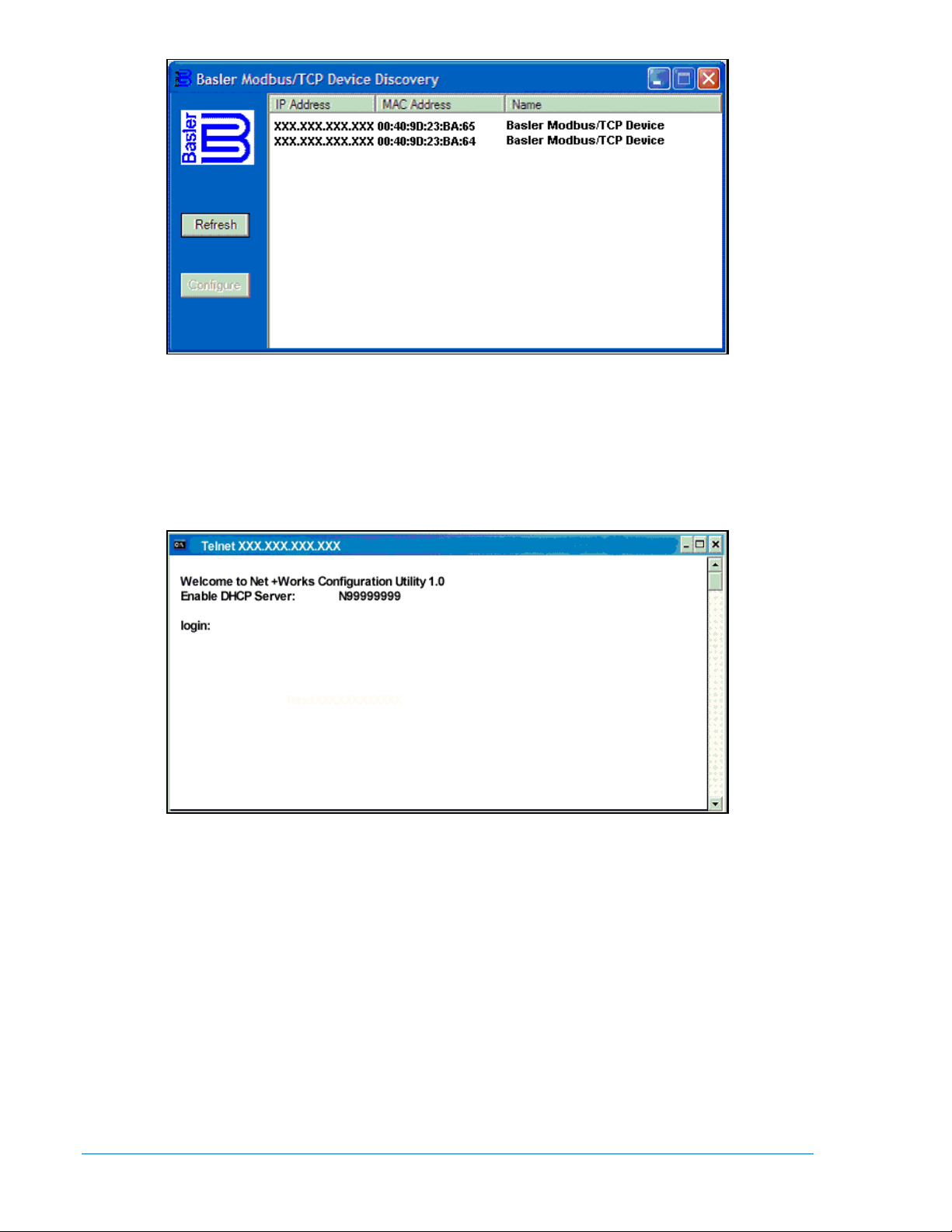
Figure 1-1. Basler Modbus/TCP Device Discovery Screen
Obtain the factory test report which is included with each BE1-700 relay and locate the MAC address.
Highlight the IP address of the relay that you wish to configure. The IP address of interest will correspond
with the MAC address shown on the factory test report. After highlighting the appropriate IP address, click
the Configure button. This will launch a telnet connection between your PC and the corresponding relay.
See Figure 1-2.
Figure 1-2. DOS Configuration Utility Screen - Login
The default parameters to log in are:
Login: root <Enter>
Password: Netsilicon
The password is case sensitive, so only the first letter should be capitalized. Press the Enter key. Once
login is successful, the screen shown in Figure 1-3 will appear.
1-4 BE1-700 Modbus™ Protocol 9376700991 Rev D
Page 15
Figure 1-3. DOS Configuration Utility Screen - Password
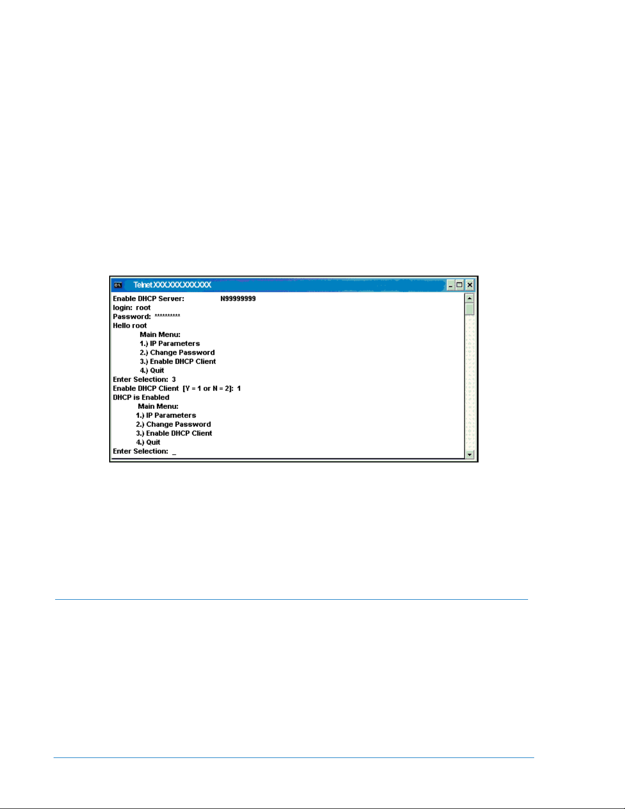
Type 3 (Enable DHCP Client) and press the Enter key. Figure 1-4 will appear. Note: This process (i.e.,
Enable DHCP Client)
You will be prompted to enable the DHCP client with a YES (1) or disable it with a NO (2). Type 2 to
disable the DHCP Client and press the Enter key. After a few seconds, the following screen (Figure 1-5)
is displayed.
must
be followed to assign a static IP address.
Figure 1-4. DOS Configuration Utility Screen – Enable DHCP Client
9376700991 Rev D BE1-700 Modbus™ Protocol 1-5
Page 16
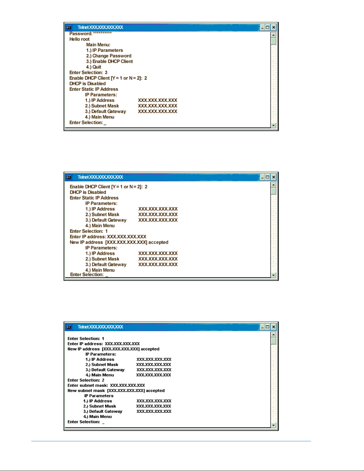
Figure 1-5. DOS Configuration Utility Screen – Don’t Enable DHCP Client
Type 1 and press the Enter key. Then type the static IP Address for the BE1-700 and press the Enter
key. A screen similar to Figure 1-6 will appear.
Figure 1-6. DOS Configuration Utility Screen – Enter IP Address
Type 2 and press the Enter key. Then type the Subnet Mask for the BE1-700 and press the Enter key. A
screen such as that shown in Figure 1-7 will appear.
Figure 1-7. DOS Configuration Utility Screen – Enter Subnet Mask
1-6 BE1-700 Modbus™ Protocol 9376700991 Rev D
Page 17
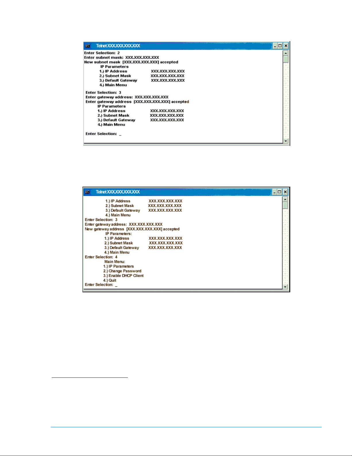
Type 3 and press the Enter key. See Figure 1-8. Then type the Default Gateway address for the BE1700 and press the Enter key.
Figure 1-8. DOS Configuration Utility Screen – Enter Default Gateway
Type 4 and press the Enter key. After a few seconds a screen similar to the one shown in Figure 1-9 will
appear.
Figure 1-9. DOS Configuration Utility Screen – Return to Main Menu
At this time, the screen refreshes with the new IP parameters. The information that was changed is saved
but it will take a few seconds for the save operation to complete. Also, from the Main Menu, the user is
encouraged to change the password from the default value.
To quit and exit the DOS window, type 4 and press the Enter key or click the X in the upper right hand
corner of the screen. In order to finish the IP setting procedure, it will be necessary to cycle the relay
power. This resets the parameters. Once this is completed, as a self-check, wait about 90 seconds and
run the Discovery program again to verify that the IP parameters are correct. Then exit the configuration
utility program. The relay is now ready to communicate with the PC.
Verifying or Setting the DHCP
This protocol assigns a dynamic IP addresses to devices on a network. With dynamic addressing, a
device can have a different IP address every time it connects to the network. Since this may not be
desirable within a company’s local area network, the IP address may have to be set statically. That is,
DHCP will have to be disabled and a permanent IP assigned as previously discussed. Previously shown
figures will be referenced in the following discussion on enabling the DHCP.
9376700991 Rev D BE1-700 Modbus™ Protocol 1-7
Page 18
Start the Basler Modbus/TCP Device Discovery application that can be found on the CD provided with the
relay. See Figure 1-1. Using the Ethernet port on the relay, make sure the relay is connected to the
company network. Be aware that it takes about 90 seconds after powering up a relay before it can be
discovered.
Clicking the Refresh button displays all Web-enabled units connected to the network. Highlight the
connection (i.e., your IP address) that you wish to configure. The IP address of interest will be related to
the MAC address shown on the factory test report. After highlighting the appropriate IP Address, click the
Configure button. This will launch a telnet application connected to the corresponding relay. See Figure
1-2.
The default parameters to login are:
Login: root <Enter>
Password: Netsilicon
The password is case sensitive, so only the first letter should be capitalized. Press the Enter key. Once
login is successful, a screen similar to the one shown in Figure 1-3 will come up.
Type 3 (Enable DHCP Client) and press the Enter key. Figure 1-4 will appear.
You will be prompted to enable the DHCP client with a YES (1) or disable it with a NO (2). Type1 and
press the Enter key. The response will be “DHCP is Enabled” as shown in Figure 1-10.
Figure 1-10. DOS Configuration Utility Screen – Enable DHCP Client
In addition, from the Main Menu, the user is encouraged to change the password from the default value.
Once the new password is changed, type 4 and press the Enter key to exit the program or click the X in
the upper right hand corner of the screen. The information that was changed is saved but it will take a few
seconds for the save operation to complete. In order to finish the setup procedure, it will be necessary to
cycle the relay power. This resets the parameters. Once this is completed, as a self-check, wait about 90
seconds and run the Discovery program again to verify that the DHCP client has been enabled. Then exit
the configuration utility program. The relay is now ready to communicate with the PC.
Change from DHCP to Static IP Address on a Single Wire Network (Between PC and BE1-700)
1) To discover the IP address of a single BE1-700 relay on an Ethernet network, the BE1-700 must be
connected to a hub or network switch that your PC’s NIC (Network Interface Card) is also connected
to. This is typically done by connecting a CAT 5 (Category 5) Ethernet cable from your PC’s NIC to a
network hub or switch and connecting the Ethernet port of the BE1-700 to the same network hub or
switch with a second CAT 5 Ethernet cable.
2) Your PC’s NIC can also be directly connected to the Ethernet port on the BE1-700 if you use a
Crossover CAT5 Ethernet cable between them.
3) In most Ethernet networks, a DHCP (Dynamic Host Configuration Protocol) server from a router or
another PC is connected to your Ethernet network through the hub or switch mentioned in step 1
above. If there is NO DHCP server, then a default 169.254.xxx.xxx IP address will be set by your PC
and by the BE1-700 after connecting the Ethernet cables. This may take a few minutes after the
cables are connected.
1-8 BE1-700 Modbus™ Protocol 9376700991 Rev D
Page 19
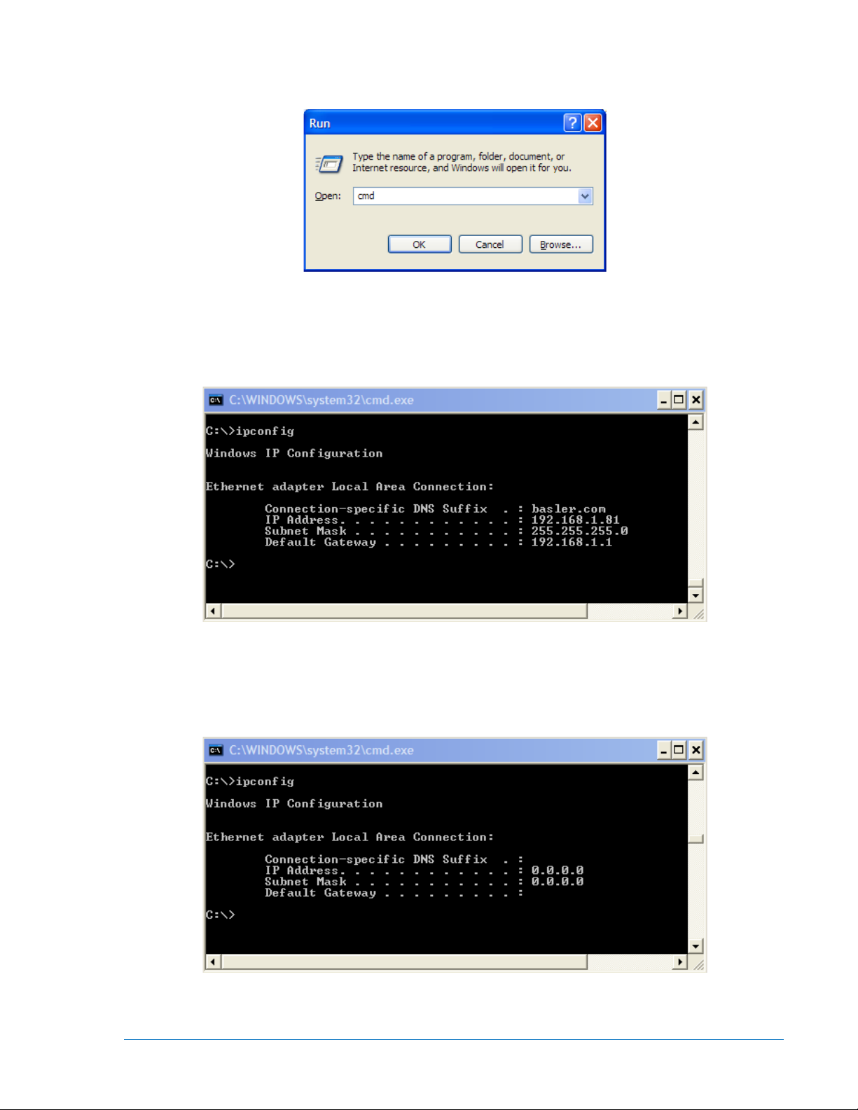
4) Testing your network can be done from your computer’s DOS command shell. To open a DOS
command shell in Windows®, select the Start RUN Open: cmd. (Figure 1-11).
Figure 1-11. DOS Command Shell
5) Example WITH a DHCP server
In the DOS command shell type ipconfig to see the available networks (Figure 1-11):
Figure 1-12. DOS Command Example with DHCP Server
6) Example WITHOUT a DHCP server
In the DOS command shell type ipconfig to see the available networks (Figure 1-13):
Figure 1-13. DOS Command Example without DHCP Server
After a few minutes (when a DHCP server is not detected) a default IP address with the format
169.254.xxx.xxx address will be reported. (Figure 1-14)
9376700991 Rev D BE1-700 Modbus™ Protocol 1-9
Page 20

Figure 1-14. DOS Command Example of Default IP Address Detected
7) Once your PC has an IP address, the BE1-700 BESTCOMS™ PC software program or the Digi
Discovery program (dgdiscvr.exe) can be used to determine the IP address of the BE1-700. A BE1700 with style number xxxxx7x (Modbus/TCP over Ethernet) must use the Modbus ping software
program (ruiping.exe)
8) In the Basler Modbus/TCP Device Discovery program, click on Refresh to discover the IP address.
Communications Hardware Requirements
RTU Communication Requirements
The BE1-700 RS-485 physical interface is three positions of a terminal strip with locations for
Send/Receive A (A), Send/Receive B (B) and Signal Ground (C). Refer to the BE1-700 Instruction Manual
(9376700990) for further details.
TCP Communication Requirements
The BE1-700 Ethernet port (RJ-45) is used with the Ethernet option. The relay supports 10BaseT using
Cat 5 / Cat 5e shielded twisted pair. Refer to the BE1-700 Instruction Manual (9376700990) for further
details.
Detailed Message Query and Response
A detailed description of BE1-700 supported message queries and responses is provided in the following
paragraphs.
Read Holding Registers
Query
This query message requests a register or block of registers to be read. The data block contains the
starting register address and the quantity of registers to be read. A register address of N will read holding
register N+1. If the query is a broadcast (device address = 0), no response message is returned.
Device Address
Function Code = 03 (hex)
Starting Address Hi
Starting Address Lo
No. of Registers Hi
No. of Registers Lo
CRC Hi error check
CRC Lo error check
The number of registers cannot exceed 125 without causing an error response with the exception code
for an illegal function.
1-10 BE1-700 Modbus™ Protocol 9376700991 Rev D
Page 21

Response
The response message contains the data queried. The data block contains the block length in bytes
followed by the data (one Data Hi byte and one Data Lo byte) for each requested register.
Reading an unassigned holding register returns a value of zero.
Device Address
Function Code = 03 (hex)
Byte Count
Data Hi (For each requested register, there is one Data Hi and one Data Lo.)
Data Lo
.
.
Data Hi
Data Lo
CRC Hi error check
CRC Lo error check
Return Query Data
This query contains data to be returned (looped back) in the response. The response and query
messages should be identical. If the query is a broadcast (device address = 0), no response message is
returned.
Device Address
Function Code = 08 (hex)
Subfunction Hi = 00 (hex)
Subfunction Lo = 00 (hex)
Data Hi = xx (don't care)
Data Lo = xx (don't care)
CRC Hi error check
CRC Lo error check
Restart Communications Option
This query causes the remote communications function of the BE1-700 to restart, terminating an active
listen only mode of operation. No effect is made upon primary relay operations. Only the remote
communications function is affected. If the query is a broadcast (device address = 0), no response
message is returned.
If the BE1-700 receives this query while in the listen only mode, no response message is generated.
Otherwise, a response message identical to the query message is transmitted prior to the
communications restart.
Device Address
Function Code = 08 (hex)
Subfunction Hi = 00 (hex)
Subfunction Lo = 01 (hex)
Data Hi = xx (don't care)
Data Lo = xx (don't care)
CRC Hi error check
CRC Lo error check
Listen Only Mode
This query forces the addressed BE1-700 to the listen only mode for Modbus communications isolating it
from other devices on the network. No responses are returned.
While in the listen only mode, the BE1-700 continues to monitor all queries. The BE1-700 does not
respond to any other query until the listen only mode is removed. All write requests with a query to Preset
Multiple Registers (Function Code = 16) are also ignored. When the BE1-700 receives the restart
communications query, the listen only mode is removed.
Device Address
Function Code = 08 (hex)
9376700991 Rev D BE1-700 Modbus™ Protocol 1-11
Page 22

Subfunction Hi = 00 (hex)
Subfunction Lo = 04 (hex)
Data Hi = xx (don't care)
Data Lo = xx (don't care)
CRC Hi error check
CRC Lo error check
Preset Multiple Registers
A preset multiple registers query could address multiple registers in one slave or multiple slaves. If the
query is a broadcast (device address = 0), no response message is returned.
Query
A Preset Multiple Register query message requests a register or block of registers to be written. The data
block contains the starting address and the quantity of registers to be written followed by the Data Block
byte count and data. The BE1-700 will perform the write when the device address is the same as the
BE1-700's remote address or when the device address is 0. A device address is 0 for a broadcast query.
A register address of N will write Holding Register N+1.
Data will cease to be written if any of the following exceptions occur:
• Queries to write to Read Only registers result in an error response with Exception Code of "Illegal
Data Address.”
• Queries attempting to write more than 100 registers cause an error response with Exception
Code "Illegal Function.”
• An incorrect Byte Count will result in an error response with Exception Code of "Illegal Data
Value.”
• There are several instances of registers that are grouped together to collectively represent a
single numerical BE1-700 data value (i.e., floating point data and 32-bit integer data). A query to
write a subset of such a register group will result in an error response with Exception Code
"Illegal Data Address.”
• A query to write a not allowed value (out of range) to a register results in an error response with
Exception Code of "Illegal Data Value.”
Device Address
Function Code = 10 (hex)
Starting Address Hi
Starting Address Lo
No. of Registers Hi
No. of Registers Lo
Byte Count
Data Hi
Data Lo
.
.
.
Data Hi
Data Lo
CRC Hi error check
CRC Lo error check
Response
The response message echoes the starting address and the number of registers. There is no response
message when the query is a broadcast (device address = 0).
Device Address
Function Code = 10 (hex)
Starting Address Hi
Starting Address Lo
No. of Registers Hi
No. of Registers Lo
CRC Hi Error Check
CRC Lo Error Check
1-12 BE1-700 Modbus™ Protocol 9376700991 Rev D
Page 23

Preset Single Register (Write Single Holding Register)
A Preset Single Register query message requests a single register to be written. The BE1-700 will
perform the write when the device address is the same as the BE1-700's remote address.
Query
Data will cease to be written if any of the following exceptions occur:
• Queries to write to Read Only registers result in an error response with Exception Code of Illegal
Data Address.
• A query to write an unallowed value (out of range) to a register results in an error response with
Exception Code of "Illegal Data Value.”
Device Address
Function Code = 06 (hex)
Address Hi
Address Lo
Data Hi
Data Lo
CRC Hi error check
CRC Lo error check
Response
The response message echoes the Query message after the register has been altered.
Data Formats
BE1-700 data varies from one to four bytes in length. Single byte data resides in the holding register
least-significant byte with the most-significant byte set to zero. Floating point data and long integer data
(each 32-bits in length) place the two most-significant bytes in the higher holding register address of the
associated register pair.
Floating Point Data Format (FP)
The Modbus floating point data format uses two consecutive holding registers to represent a data value.
The first register contains the low-order 16 bits of the following 32 bit format:
• MSB is the sign bit for the floating point value (0 = positive).
• The next 8 bits are the exponent biased by 127 decimal.
• The 23 LSBs comprise the normalized mantissa. The most-significant bit of the mantissa is
always assumed to be 1 and is not explicitly stored, yielding an effective precision of 24 bits.
The value of the floating point number is obtained by multiplying the binary mantissa times two raised to
the power of the unbiased exponent. The assumed bit of the binary mantissa has the value of 1.0, with
the remaining 23 bits providing a fractional value. Table 1-3 shows the floating point format.
Table 1-3. Floating Point Format
Sign Exponent +127 Mantissa
1 bit 8 bits 23 bits
The floating point format allows for values ranging from approximately 8.43X10-37 to 3.38X1038. A
floating point value of all zeroes is the value zero. A floating point value of all ones (not a number)
signifies a value currently not applicable or disabled.
Example: The value 95,800 represented in floating point format is hexadecimal 47BB1C00. This number
will read from two consecutive holding registers as follows:
Holding Register
K (Hi Byte) hex 1C
K (Lo Byte) hex 00
K+1 (Hi Byte) hex 47
K+1 (Lo Byte) hex BB
9376700991 Rev D BE1-700 Modbus™ Protocol 1-13
Value
Page 24

The same byte alignments are required to write.
Long Integer Data Format (LI)
The Modbus long integer data format uses two consecutive holding registers to represent a 32 bit data
value. The first register contains the low-order 16 bits and the second register contains the high-order 16
bits.
Example: The value 95,800 represented in long integer format is hexadecimal 0x00017638. This number
will read from two consecutive holding registers as follows.
Holding Register
K (Hi Byte) hex 76
K (Lo Byte) hex 38
K+1 (Hi Byte) hex 00
K+1 (Lo Byte) hex 01
The same byte alignments are required to write.
Value
Integer Data Format (INT)
The Modbus integer data format uses a single holding register to represent a 16 bit data value.
Example: The value 4660 represented in integer format is hexadecimal 0x1234. This number will read
from a holding register as follows:
Holding Register
K (Hi Byte) hex 12
K (Lo Byte) hex 34
The same byte alignments are required to write.
Value
Short Integer Data Format (SI)
The Modbus short integer data format uses a single holding register to represent an 8 bit data value. The
holding register high byte will always be zero.
Example: The value 132 represented in short integer format is hexadecimal 0x84. This number will read
from a holding register as follows:
Holding Register
K (Hi Byte) hex 00
K (Lo Byte) hex 84
The same byte alignments are required to write.
ASCII Character Data Format (ASC(1))
The Modbus ASCII character data format uses a single holding register to represent a single character
value. The holding register high byte will always be zero with the ASCII character code in the low byte.
Example: The character 'D' represented in ASCII character format is hexadecimal 44. This number will
read from a holding register as follows:
Holding Register
K (Hi Byte) hex 00
K (Lo Byte) hex 44
The same byte alignments are required to write.
Value
Value
ASCII String Data Format (ASC(x))
The Modbus ASCII string data format uses one or more holding registers to represent a sequence or
string of character values. If the string contains a single character, the holding register high byte will
contain the ASCII character code and the low byte will be zero.
Example: The string "PASSWORD" represented in ASCII string format will read as follows:
1-14 BE1-700 Modbus™ Protocol 9376700991 Rev D
Page 25

Holding Register
K (Hi Byte) 'P'
K (Lo Byte) 'A'
K+1 (Hi Byte) 'S'
K+1 (Lo Byte) 'S'
K+2 (Hi Byte) 'W'
K+2 (Lo Byte) 'O'
K+3 (Hi Byte) 'R'
K+3 (Lo Byte) 'D'
Example: If the above string is changed to "P", the new string will read as follows:
Holding Register
K (Hi Byte) 'P'
K (Lo Byte) hex 00
K+1 (Hi Byte) hex 00
K+1 (Lo Byte) hex 00
K+2 (Hi Byte) hex 00
K+2 (Lo Byte) hex 00
K+3 (Hi Byte) hex 00
K+3 (Lo Byte) hex 00
The same byte alignments are required to write.
Value
Value
Bit Mapped Data Format (BM(x))
The bit mapped data format uses two or more holding registers to represent a sequence of bit values. The
Modbus Bit Map data format can represent an 8 bit, 16 bit, 32 bit or 64 bit value.
Example: The Bit Map value of the hexadecimal number 0x123456789ABCDEF0 using a BM64 format
will read as follows:
Holding Register
K (Hi Byte) 0x12
K (Lo Byte) 0x34
K+1 (Hi Byte) 0x56
K+1 (Lo Byte) 0x78
K+2 (Hi Byte) 0x9A
K+2 (Lo Byte) 0xBC
K+3 (Hi Byte) 0xDE
K+3 (Lo Byte) 0xF0
Value
CRC Error Check
This field contains a two-byte CRC value for transmission error detection. The master first calculates the
CRC and appends it to the query message. The BE1-700 recalculates the CRC value for the received
query and performs a comparison to the query CRC value to determine if a transmission error has
occurred. If so, no response message is generated. If no transmission error has occurred, the slave
calculates a new CRC value for the response message and appends it to the message for transmission.
The CRC calculation is performed using all bytes of the device address, function code and data block
fields. A 16-bit CRC-register is initialized to all 1's. Then each eight-bit byte of the message is used in the
following algorithm:
First, exclusive-OR the message byte with the low-order byte of the CRC-register. The result, stored in
the CRC-register, will then be right-shifted eight times. The CRC-register MSB is zero-filled with each
shift. After each shift, the CRC-register LSB is examined. If the LSB IS a 1, the CRC-register is then
exclusive-ORed with the fixed polynomial value A001 (hex) prior to the next shift. Once all bytes of the
message have undergone the above algorithm, the CRC-register will contain the message CRC value to
be placed in the error check field.
Session Access Registers
The ACCESS REQUEST and the EXIT registers are used to access and release write privileges while
changing relay settings, resetting report registers, or using control commands through the Modbus port.
This feature is important because it prevents changes from being made concurrently from two areas. For
9376700991 Rev D BE1-700 Modbus™ Protocol 1-15
Page 26

example, a user cannot make changes from COM0 at the same time a remote user is making changes
via Modbus from COM2.
Changing the settings through the Modbus port requires that the operator write to the ACCESS
REQUEST register to obtain programming access. This must follow writing the ACCESS PASSWORD
register(s) with a password to obtain access to change settings associated with the password. Different
passwords give the ability or access to perform different operations. The relay will deny access if an
invalid password is entered or if another user has already been granted programming access through
another serial port or at the front panel. Only one user can have access at any one time.
If no password protection is used, it is still necessary to obtain access in order to protect against
accidental changes. If password protection is disabled, then writing the ACCESS REQUEST register will
be accepted in place of a password. The relay will transmit a valid response message if the access query
was received and executed. The relay will respond with an error message if the access query could not
be executed.
Changing settings through a Modbus communication port consists of the following sequence:
Step 1. Preset Multiple Registers query to ACCESS PASSWORD register(s) to specify password.
Step 2. Preset Multiple Registers query to ACCESS REQUEST register to access write privileges.
Step 3. Preset Multiple Registers queries to change the current settings.
Step 4. Preset Multiple Registers query to EXIT register to clear access and save.
Changes are not made to the working settings but to a scratch-pad copy of the settings. After the
change(s) are made, the new data will be copied to the working settings and saved to non-volatile
memory when the EXIT register is written with a 'Y.' It is important to make all changes to relay
parameters before writing the EXIT register. This prevents a partial or incomplete protection scheme from
being implemented.
Template Registers
The BE1-700 uses three templates. A template is a block of holding registers to which the user assigns
one of a number of similar groups of parameters. Templates are used for settings groups, fault
summaries, and report generation. Modbus Template Registers 40036 (Settings Group Selection), 40038
(Fault Number Selection), 40039 (Report Selection) and 40040 (Report Focus) do not require any Write
Password Access level before they can be written to.
The BE1-700 has two settings groups. The GRP template is assigned the parameters of a settings group.
Therefore, before reading or writing settings group values, a user must first specify which settings group
is to be associated with the template. This is accomplished by writing the desired settings group number
(0 or 1) into the SETTINGS GROUP SELECTION Template holding register.
The BE1-700 stores up to 12 faults. Each fault is accessed by its fault number which ranges from 1 to
255. The FLT template is assigned the parameters of a particular fault occurrence. Therefore, before
reading fault summary values, a user must first specify which fault number is to be associated with the
template. This is accomplished by writing the desired fault number (1-255) into the FAULT SELECTION
Template holding register.
The BE1-700 generates 10 ASCII reports. The RPT template is assigned the text of a report. Therefore,
before reading report text, a user must first specify which report is to be associated with the template.
This is accomplished by writing the desired report number into the REPORT SELECTION Template
holding register along with the associated report identifier, if any, into the REPORT FOCUS Template
holding register.
Fault Summary Registers
The user can enter any fault number (1 - 255) into the FAULT SELECTION Template holding register to
associate summary parameters for that fault number with the FLT Template. The Fault Template Status
register (47513) indicates whether or not that fault number specifies a recent fault (one of 12 stored
faults). If so, the Fault Template Status register value is the fault number. Otherwise, it is zero and all FLT
template values will read zero.
The Fault Indicator register (47512) value is the fault number (1 - 255) of the most recent fault. The user
may construct his front-end GUI to link this register value into the FAULT SELECTION Template holding
register, thereby automatically associating the FLT template with the most recent fault occurrence.
1-16 BE1-700 Modbus™ Protocol 9376700991 Rev D
Page 27

Report Generation Registers
The BE1-700 generates numerous ASCII reports available via serial commands. Several of these reports
are available intact via the Modbus communication port. The desired report is first specified by writing the
REPORT SELECTION holding register. If the report requires a number to be specified such as a fault
number or number of events, that number is written into the REPORT FOCUS holding register. The report
is then available via the RPT template. The report can be read from 1 to 125 registers at a time, with each
register containing 2 ASCII characters of information. The report read queries can be interspersed among
other query types. The RPT template is continually re-read until the report has completed. Once the
report is complete, reading from the RPT template will continually return the ASCII character code of 127
("7F" hexadecimal). The report cannot be re-read or another report read until the REPORT SELECTION
holding register is re-written.
Contiguous Poll Block Registers
The user may allocate up to 125 holding registers to the Contiguous Poll Block (49875-999). This
allocation allows dispersed registers which are frequently read to be polled via a single read query. A
register is assigned to a position in the Poll Block by writing its address value into the corresponding
position in the Contiguous Poll Block Assignments registers (40746-870). Writing a zero value leaves that
Poll Block position unassigned. Once assignments are made, the values of the assigned registers may be
read by polling the Contiguous Poll Block. Polling an unassigned position will return a value of zero.
For example, if you wanted to continuously monitor the Date (47364), Time (47365-66), Fault Indicator
(47512) and Breaker Status (47390g) Holding Registers, you would first configure the Contiguous Poll
Block Registers by writing the desired register address values 7364, 7365, 7366, 7512 and 7388 into the
Contiguous Poll Block Assignment registers 40746 thru 40750, respectively. You may now begin
monitoring the specified registers by reading the first 5 locations in the Contiguous Poll Block; i.e., reading
register 49875 for the Date (as specified in it's corresponding assignment register 40746), reading
register 49876 and 77 for the Time (as specified in their corresponding assignment registers 40747 and
48), reading register 49878 for the Fault Indicator (as specified in it's corresponding assignment register
40749) and reading register 49879 for the Breaker Status (as specified in it's corresponding assignment
register 40750).
Exception Code Enhancement Registers
When a BE1-700 responds to a Preset Multiple Register query with an error response message,
additional information detailing the cause of the error may be available in the ERROR DETAILS block of
holding registers (49835-54). The information is in ASCII format and available by reading the message
string from the ERROR DETAILS block. The message remains available until the next Preset Multiple
Register query is executed unless that query is to the FAULT SELECTION Template holding register.
Since this register can be written automatically and randomly in time, the ERROR DETAILS block will not
be updated.
The ERROR DETAILS block will also contain the exit status following a Preset Multiple Register query to
the EXIT (40001) register. You may clear the ERROR DETAILS message at any time without affecting
system operation by sending a Preset Multiple Register query to any unassigned holding register.
9376700991 Rev D BE1-700 Modbus™ Protocol 1-17
Page 28

1-18 BE1-700 Modbus™ Protocol 9376700991 Rev D
Page 29

SECTION 2 • REGISTER TABLE
Mapping BE1-700 Parameters into Modicon Holding Register Address Space
General
Parameters are mapped into the holding register address space (40001 - 49999) in blocks according to
access type.
Any Holding Register not listed in the Register Table is an unassigned Holding Register. A value of zero
always results when reading an unassigned Holding Register. Writes to unassigned Holding Registers are
legal but no action will be taken (the write is ignored).
Conventions
The Data Format column uses the following abbreviations:
ASC(x) - ASCII string, where x = the maximum defined string length
BM(x) - Bit-map, where x = the number of related bits
FP - Floating point
INT - Integer (16-bit integer)
LI - Long Integer (32-bit integer)
SI - Short Integer (8-bit integer)
The Notes column uses the following abbreviations:
GRP Group Template Member
FLT Fault Template Member
RPT Report Template Member
NS Not Supported
TS Time Stamp format: MSEC of the day (0 to 86,400,000 ms) and DAYs since 01/01/1984.
PS Effective only when the Password Security parameter is enabled. See REGISTER
DETAILS for Password Security holding register 40989.
PW Effective for any communication port active with ASCII protocol and for the Modbus™ port
(COM 2) when Password Security is enabled.
Register Table - Ordered By Register Number
9376700991 Rev D BE1-700 Modbus™ Protocol 2-1
Page 30

Holding Read/Write Data
Register Parameter Supported Format Notes
Session Parameters
40001 Exit R W ASC(1) PS
40002-05 Access Password R W ASC(8) PS
40006 Access Request R W BM(16) PS
Template Parameters
40036 Settings Group Selection R W SI
40038 Fault Selection R W SI
40039 Report Selection R W SI
40040 Report Focus R W INT
Global Parameters
40080-83 Global Password R W ASC(8) PW
40084 Global Path R W BM(8) PW
40085-88 Setting Password R W ASC(8) PW
40089 Setting Path R W BM(8) PW
40090-93 Control Password R W ASC(8) PW
40094 Control Path R W BM(8) PW
40095-98 Report Password R W ASC(8) PW
40099 Report Path R W BM(8) PW
Control Parameters
40117 Select Group R W ASC(1)
40118 Operate Group R W ASC(1)
40119 Select Virtual Selector Switch 43 R W ASC(1)
40120 Operate Virtual Selector Switch 43 R W ASC(1)
40121 Select Virtual Selector Switch 143 R W ASC(1)
40122 Operate Virtual Selector Switch 143 R W ASC(1)
40135 Select 101 Virtual Breaker Control Switch R W ASC(1)
40136 Operate 101 Virtual Breaker Control Switch R W ASC(1)
40137 Select All Outputs R W ASC(1)
40138 Operate All Outputs R W ASC(1)
40139 Select Output A R W ASC(1)
40140 Operate Output A R W ASC(1)
40141 Select Output 1 R W ASC(1)
40142 Operate Output 1 R W ASC(1)
40143 Select Output 2 R W ASC(1)
40144 Operate Output 2 R W ASC(1)
40145 Select Output 3 R W ASC(1)
40146 Operate Output 3 R W ASC(1)
40147 Select Output 4 R W ASC(1)
40148 Operate Output 4 R W ASC(1)
40149 Select Output 5 R W ASC(1)
40150 Operate Output 5 R W ASC(1)
2-2 BE1-700 Modbus™ Protocol 9376700991 Rev D
Page 31

Holding Read/Write Data
Register Parameter Supported Format Notes
Group Setting Parameters
The following is the Group Template (GRP)
40259-60 50TP Pickup R W FP GRP
40261-62 50TP Time Delay R W LI GRP
40263 50TP Directional Mode R W ASC(1) GRP
40264-65 50TN Pickup R W FP GRP
40266-67 50TN Time Delay R W LI GRP
40268 50TN Directional Mode R W ASC(1) GRP
40269-70 50TQ Pickup R W FP GRP
40271-72 50TQ Time Delay R W LI GRP
40273 50TQ Directional Mode R W ASC(1) GRP
40274-75 150TP Pickup R W FP GRP
40276-77 150TP Time Delay R W LI GRP
40278 150TP Directional Mode R W ASC(1) GRP
40279-80 150TN Pickup R W FP GRP
40281-82 150TN Time Delay R W LI GRP
40283 150TN Directional Mode R W ASC(1) GRP
40284-85 150TQ Pickup R W FP GRP
40286-87 150TQ Time Delay R W LI GRP
40288 150TQ Directional Mode R W ASC(1) GRP
40301-02 51P Pickup R W FP GRP
40303-04 51P Time Dial R W FP GRP
40305-06 51P Curve Type R W ASC(3) GRP
40307 51P Directional Mode R W ASC(1) GRP
40308-09 51N Pickup R W FP GRP
40310-11 51N Time Dial R W FP GRP
40312-13 51N Curve Type R W ASC(3) GRP
40314 51N Directional Mode R W ASC(1) GRP
40315-16 51Q Pickup R W FP GRP
40317-18 51Q Time Dial R W FP GRP
40319-20 51Q Curve Type R W ASC(3) GRP
40321 51Q Directional Mode R W ASC(1) GRP
40322-23 151P Pickup R W FP GRP
40324-25 151P Time Dial R W FP GRP
40326-27 151P Curve Type R W ASC(3) GRP
40329-30 151N Pickup R W FP GRP
40331-32 151N Time Dial R W FP GRP
40333-34 151N Curve Type R W ASC(3) GRP
40335 151N Directional Mode R W ASC(1) GRP
40359-60 62 Time Delay 1 R W LI GRP
40361-62 62 Time Delay 2 R W LI GRP
40363-64 162 Time Delay 1 R W LI GRP
40365-66 162 Time Delay 2 R W LI GRP
9376700991 Rev D BE1-700 Modbus™ Protocol 2-3
Page 32

Holding Read/Write Data
Register Parameter Supported Format Notes
40406-07 79 First Automatic Reclose Delay R W LI GRP
40408-09 79 Second Automatic Reclose Delay R W LI GRP
40410-11 79 Third Automatic Reclose Delay R W LI GRP
40412-13 79 Fourth Automatic Reclose Delay R W LI GRP
40414-15 79 Reset Time Delay R W LI GRP
40416-17 79 Reclose Fail Time Delay R W LI GRP
40418-19 79 Maximum Reclose Time R W LI GRP
40420-21 79 Pilot Time Delay R W LI GRP
40422 79 Block Output R W LI GRP
40429-30 27R Pickup R W FP GRP
40431 27R Control Mode R W ASC(1) GRP
40432-33 47 Pickup R W FP GRP
40434-35 47 Time Delay R W LI GRP
40436-37 59P Pickup R W FP GRP
40438-39 59P Time Delay R W LI GRP
40440-41 59X Pickup R W FP GRP
40442-43 59X Time Delay R W LI GRP
40444-45 159P Pickup R W FP GRP
40446-47 159P Time Delay R W LI GRP
40448-49 159X Pickup R W FP GRP
40450-51 159X Time Delay R W LI GRP
40460-61 81 Pickup R W FP GRP
40462-63 81 Time Delay R W LI GRP
40464 81 Mode R W ASC(1) GRP
40465-66 181 Pickup R W FP GRP
40467-68 181 Time Delay R W LI GRP
40469 181 Mode R W ASC(1) GRP
40470-71 281 Pickup R W FP GRP
40472-73 281 Time Delay R W LI GRP
40474 281 Mode R W ASC(1) GRP
40475-76 381 Pickup R W FP GRP
40477-78 381 Time Delay R W LI GRP
40479 381 Mode R W ASC(1) GRP
40480-81 481 Pickup R W FP GRP
40482-83 481 Time Delay R W LI GRP
40484 481 Mode R W ASC(1) GRP
40485-86 581 Pickup R W FP GRP
40487-88 581 Time Delay R W LI GRP
40489 581 Mode R W ASC(1) GRP
40490-91 81 Phase A Voltage Inhibit Setting R W FP GRP
40492-93 81 Negative-Sequence Voltage Inhibit Setting R W FP GRP
40494-95 81 Overfrequency Inhibit Setting R W FP GRP
40496-97 81 Underfrequency Inhibit Setting R W FP GRP
2-4 BE1-700 Modbus™ Protocol 9376700991 Rev D
Page 33

Holding Read/Write Data
Register Parameter Supported Format Notes
40498-99 27P Pickup R W FP GRP
40500-01 27P Time Delay R W LI GRP
40502-03 27P Inhibit Voltage R W FP GRP
40504-05 27X Pickup R W FP GRP
40506-07 27X Time Delay R W LI GRP
40508-09 27X Inhibit Voltage R W FP GRP
40510-11 127P Pickup R W FP GRP
40512-13 127P Time Delay R W LI GRP
40514-15 127P Inhibit Voltage R W FP GRP
40516-17 24 Pickup R W FP GRP
40518-19 24 Time Delay R W FP GRP
40520-21 24 Reset Delay R W FP GRP
40522-23 24 Definite Timer 1 Pickup R W FP GRP
40524-25 24 Definite Timer 1 Time Delay R W LI GRP
40526-27 24 Definite Timer 2 Pickup R W FP GRP
40528-29 24 Definite Timer 2 Time Delay R W LI GRP
40530-31 24 Curve Type R W ASC(3) GRP
40532-33 25 Volts R W FP GRP
40534-35 25 Angle R W FP GRP
40536-37 25 Slip R W FP GRP
40538 25 Mode R W INT GRP
40539-40 25VM Live Volts R W FP GRP
40541-42 25VM Dead Volts R W FP GRP
40543-44 25VM Time Delay R W LI GRP
40545-46 25VM Mode1 R W ASC(3) GRP
Global Setting Parameters
40602-03 Power System Nominal Voltage R W FP
40604-05 Power System Nominal Current R W FP
40606-07 Breaker Fail Time Delay R W LI
40608-09 Programmable 51 Curve Constant A R W FP
40610-11 Programmable 51 Curve Constant B R W FP
40612-13 Programmable 51 Curve Constant C R W FP
40614-15 Programmable 51 Curve Constant N R W FP
40616-17 Programmable 51 Curve Constant R R W FP
40618 Input 1 Contact Recognition Time Delay R W SI
40619 Input 1 Contact Debounce Time Delay R W SI
40620 Input 2 Contact Recognition Time Delay R W SI
40621 Input 2 Contact Debounce Time Delay R W SI
40622 Input 3 Contact Recognition Time Delay R W SI
40623 Input 3 Contact Debounce Time Delay R W SI
40624 Input 4 Contact Recognition Time Delay R W SI
40625 Input 4 Contact Debounce Time Delay R W SI
40746-870 Contiguous Poll Block Assignments R W INT
40871 Setting Group Control On Time R W INT
9376700991 Rev D BE1-700 Modbus™ Protocol 2-5
Page 34

Holding Read/Write Data
Register Parameter Supported Format Notes
40872 Setting Group 1 Automatic Control Switch Time R W SI
40873 Setting Group 1 Automatic Control Switch Level R W SI
40874 Setting Group 1 Automatic Control Time R W SI
40875 Setting Group 1 Automatic Control Return Level R W SI
40876 Setting Group 1 Tracking Element R W INT
40887-92 79 Zone-Sequence Logic Mask R W BM(96)
40895-900 79 Zone-Sequence Logic Term R W BM(96)
40903-04 60FL Loss of Pot. Current Auto Block Setting R W ASC(3)
40905-06 60FL Loss of Potential Volt. Auto Block Setting R W ASC(3)
Serial Port Setting Parameters
40962 Serial Port 0 Baud Rate R W INT
40964 Serial Port 0 Software Flow Control R W SI
40965 Serial Port 0 Page Length R W SI
40966 Serial Port 0 Acknowledgement Format R W SI
40980 Serial Port 2 Baud Rate R W INT
40981 Serial Port 2 Relay Address R W INT
40986 Serial Port 2 Modbus Parity R W SI
40987 Serial Port 2 Modbus Remote Delay R W SI
40988 Serial Port 2 Modbus Stop Bits R W SI
40989 Password Security R W SI
System Data Setting Parameters
41018 System Frequency R W SI
41019-20 Phase Rotation R W ASC(3)
41021 Phase Ratio R W INT
41022 Ground CT Ratio R W INT
41033-34 Phase VT Ratio R W FP
41035-36 27/59 Voltage Sensing Mode R W ASC(3)
41037-38 51/27R Voltage Sensing Mode R W ASC(3)
41039-40 VT Connection RW ASC(3)
41041-42 Auxiliary VT Ratio R W FP
41043-44 VT Auxiliary Connection RW ASC(3)
41046-47 Power Line - Z1 Impedance R W FP
41048-49 Power Line - Z1 Angle R W FP
410450-51 Power Line - Z0 Impedance R W FP
41052-53 Power Line - Z0 Angle R W FP
41054-55 Power Line - Line Length R W FP
Breaker Duty Setting Parameters
41092-93 Breaker Duty Exponent R W FP
41094-95 Maximum Breaker Duty R W FP
41096 Programmable Breaker Alarm #1 Mode R W INT
41097-98 Programmable Breaker Alarm #1 Limit R W FP
41099 Programmable Breaker Alarm #2 Mode R W INT
41100-01 Programmable Breaker Alarm #2 Limit R W FP
2-6 BE1-700 Modbus™ Protocol 9376700991 Rev D
Page 35

Holding Read/Write Data
Register Parameter Supported Format Notes
41102 Programmable Breaker Alarm #3 Mode R W INT
41103-04 Programmable Breaker Alarm #3 Limit R W FP
41110-15 Breaker Block Logic Mask R W BM(96)
41118-23 Breaker Block Logic Term R W BM(96)
41126-31 Breaker Close Logic Mask R W BM(96)
41134-39 Breaker Close Logic Term R W BM(96)
Relay Data Setting Parameters
41247 Volts / Hertz Alarm Pickup Level R W FP
41248-49 Volts / Hertz Alarm Time Delay R W LI
41251-52 Forward Var Demand Alarm R W FP
41253-54 Reverse Var Demand Alarm R W FP
41255-56 Forward Watt Demand Alarm R W FP
41257-58 Reverse Watt Demand Alarm R W FP
41259-60 Phase Demand Alarm Level R W FP
41261-62 Neutral Demand Alarm Level R W FP
41263-64 Negative-Sequence Demand Alarm Level R W FP
41265-66 Major Alarm Mask R W BM(32)
41267-68 Minor Alarm Mask R W BM(32)
41269-70 Logic Alarm Mask R W BM(32)
41272 Clock Format - Date R W ASC(1)
41273 Clock Format - Time R W SI
41274 Clock Format - Daylight Savings R W SI
41275 Phase Demand Interval R W SI
41276 Neutral Demand Interval R W SI
41277 Negative-Sequence Demand Interval R W SI
41281 LCD Backlight Timer R W INT
41284 Output Hold Mask R W BM(8)
41285-90 Target Mask R W BM(96)
41291-94 Programmable Screen #1 R W ASC(7)
41295-98 Programmable Screen #2 R W ASC(7)
41299-302 Programmable Screen #3 R W ASC(7)
41303-06 Programmable Screen #4 R W ASC(7)
41307-10 Programmable Screen #5 R W ASC(7)
41311-14 Programmable Screen #6 R W ASC(7)
41315-18 Programmable Screen #7 R W ASC(7)
41319-22 Programmable Screen #8 R W ASC(7)
41323-26 Programmable Screen #9 R W ASC(7)
41327-30 Programmable Screen #10 R W ASC(7)
41331-34 Programmable Screen #11 R W ASC(7)
41335-38 Programmable Screen #12 R W ASC(7)
41339-42 Programmable Screen #13 R W ASC(7)
41343-46 Programmable Screen #14 R W ASC(7)
41347-50 Programmable Screen #15 R W ASC(7)
41351-54 Programmable Screen #16 R W ASC(7)
9376700991 Rev D BE1-700 Modbus™ Protocol 2-7
Page 36

Holding Read/Write Data
Register Parameter Supported Format Notes
41355-60 Fault Record Trigger (Trip) Logic Mask R W BM(96)
41363-68 Fault Record Trigger (Trip) Logic Term R W BM(96)
41371-76 Fault Record Trigger (Pickup) Logic Mask R W BM(96)
41379-84 Fault Record Trigger (Pickup) Logic Term R W BM(96)
41387-92 Fault Record Trigger (Logic) Logic Mask R W BM(96)
41395-400 Fault Record Trigger (Logic) Logic Term R W BM(96)
41403-08 Reset Target Logic Mask R W BM(96)
41411-16 Reset Target Logic Term R W BM(96)
41419-24 Reset Alarm Logic Mask R W BM(96)
41427-32 Reset Alarm Logic Term R W BM(96)
Custom Logic Setting Parameters
41465-72 User Custom Logic Name R W ASC(16)
41473-80 Current Active Logic Scheme R – ASC(16)
41481-88 Custom Logic Name R – ASC(16)
41489-96 Standard Logic #1 Name R – ASC(16)
41497-504 Standard Logic #2 Name R – ASC(16)
41505 Programmable 50TP Block Logic Mode R W INT
41506-11 Programmable 50TP Block Logic Mask R W BM(96)
41514-19 Programmable 50TP Block Logic Term R W BM(96)
41522 Programmable 50TN Block Logic Mode R W INT
41523-28 Programmable 50TN Block Logic Mask R W BM(96)
41531-36 Programmable 50TN Block Logic Term R W BM(96)
41539 Programmable 50TQ Block Logic Mode R W INT
41540-45 Programmable 50TQ Block Logic Mask R W BM(96)
41548-53 Programmable 50TQ Block Logic Term R W BM(96)
41556 Programmable 150TP Block Logic Mode R W INT
41557-62 Programmable 150TP Block Logic Mask R W BM(96)
41565-70 Programmable 150TP Block Logic Term R W BM(96)
41573 Programmable 150TN Block Logic Mode R W INT
41574-79 Programmable 150TN Block Logic Mask R W BM(96)
41582-87 Programmable 150TN Block Logic Term R W BM(96)
41590 Programmable 150TQ Block Logic Mode R W INT
41591-96 Programmable 150TQ Block Logic Mask R W BM(96)
41599-604 Programmable 150TQ Block Logic Term R W BM(96)
41658 Programmable Breaker Fail Logic Mode R W INT
41659-64 Programmable Breaker Fail Initiate Logic Mask R W BM(96)
41667-72 Programmable Breaker Fail Initiate Logic Term R W BM(96)
41675-80 Programmable Breaker Fail Block Logic Mask R W BM(96)
41683-88 Programmable Breaker Fail Block Logic Term R W BM(96)
41691 Programmable 51P Logic Mode R W INT
41692-97 Programmable 51P Block Logic Mask R W BM(96)
41700-05 Programmable 51P Block Logic Term R W BM(96)
2-8 BE1-700 Modbus™ Protocol 9376700991 Rev D
Page 37

Holding Read/Write Data
Register Parameter Supported Format Notes
41708 Programmable 51N Logic Mode R W INT
41709-14 Programmable 51N Block Logic Mask R W BM(96)
41717-22 Programmable 51N Block Logic Term R W BM(96)
41725 Programmable 51Q Logic Mode R W INT
41726-31 Programmable 51Q Block Logic Mask R W BM(96)
41734-39 Programmable 51Q Block Logic Term R W BM(96)
41759 Programmable 151N Logic Mode R W INT
41760-65 Programmable 151N Block Logic Mask R W BM(96)
41768-73 Programmable 151N Block Logic Term R W BM(96)
41809 Programmable 62 Timer Logic Mode R W INT
41810-15 Programmable 62 Timer Start Logic Mask R W BM(96)
41818-23 Programmable 62 Timer Start Logic Term R W BM(96)
41826-31 Programmable 62 Timer Block Logic Mask R W BM(96)
41834-39 Programmable 62 Timer Block Logic Term R W BM(96)
41842 Programmable 162 Timer Logic Mode R W INT
41843-48 Programmable 162 Timer Start Logic Mask R W BM(96)
41851-56 Programmable 162 Timer Start Logic Term R W BM(96)
41859-64 Programmable 162 Timer Block Logic Mask R W BM(96)
41867-72 Programmable 162 Timer Block Logic Term R W BM(96)
41875 Programmable 27P Logic Mode R W INT
41876-81 Programmable 27P Block Logic Mask R W BM(96)
41884-89 Programmable 27P Block Logic Term R W BM(96)
41892 Programmable 27X Logic Mode R W INT
41893-98 Programmable 27X Block Logic Mask R W BM(96)
41901-06 Programmable 27X Block Logic Term R W BM(96)
41909 Programmable 127P Logic Mode R W INT
41910-15 Programmable 127P Block Logic Mask R W BM(96)
41918-23 Programmable 127P Block Logic Term R W BM(96)
41943 Programmable 59P Logic Mode R W INT
41944-49 Programmable 59P Block Logic Mask R W BM(96)
41952-57 Programmable 59P Block Logic Term R W BM(96)
41960 Programmable 59X Logic Mode R W INT
41961-66 Programmable 59X Block Logic Mask R W BM(96)
41969-74 Programmable 59X Block Logic Term R W BM(96)
41977 Programmable 159P Logic Mode R W INT
41978-83 Programmable 159P Block Logic Mask R W BM(96)
41986-91 Programmable 159P Block Logic Term R W BM(96)
41994 Programmable 159X Logic Mode R W INT
41995-42000 Programmable 159X Block Logic Mask R W BM(96)
42003-08 Programmable 159X Block Logic Term R W BM(96)
42062 Programmable Settings GRP Logic Mode R W INT
42063-68 Programmable Settings GRP Block Logic Mask R W BM(96)
42071-76 Programmable Settings GRP Block Logic Term R W BM(96)
9376700991 Rev D BE1-700 Modbus™ Protocol 2-9
Page 38

Holding Read/Write Data
Register Parameter Supported Format Notes
42079-84 Programmable Set. GRP 0 Select Logic Mask R W BM(96)
42087-92 Programmable Set. GRP 0 Select Logic Term R W BM(96)
42095-100 Programmable Set. GRP 1 Select Logic Mask R W BM(96)
42103-08 Programmable Set. GRP 1 Select Logic Term R W BM(96)
42111 Programmable 43 Virtual Switch Logic Mode R W INT
42112 Programmable 143 Virtual Switch Logic Mode R W INT
42115 Program. 101 Virtual BKR CNTRL Logic Mode R W INT
42133 Programmable Virtual Output A Term Count R W SI
42134-39 Programmable Virtual Output A Logic Mask 1 R W BM(96)
42142-47 Programmable Virtual Output A Logic Term 1 R W BM(96)
42150-55 Programmable Virtual Output A Logic Mask 2 R W BM(96)
42158-63 Programmable Virtual Output A Logic Term 2 R W BM(96)
42166-71 Programmable Virtual Output A Logic Mask 3 R W BM(96)
42174-79 Programmable Virtual Output A Logic Term 3 R W BM(96)
42182-87 Programmable Virtual Output A Logic Mask 4 R W BM(96)
42190-95 Programmable Virtual Output A Logic Term 4 R W BM(96)
42198 Programmable Virtual Output 1 Term Count R W SI
42199-204 Programmable Virtual Output 1 Logic Mask 1 R W BM(96)
42207-12 Programmable Virtual Output 1 Logic Term 1 R W BM(96)
42215-20 Programmable Virtual Output 1 Logic Mask 2 R W BM(96)
42223-28 Programmable Virtual Output 1 Logic Term 2 R W BM(96)
42231-36 Programmable Virtual Output 1 Logic Mask 3 R W BM(96)
42239-44 Programmable Virtual Output 1 Logic Term 3 R W BM(96)
42247-52 Programmable Virtual Output 1 Logic Mask 4 R W BM(96)
42255-60 Programmable Virtual Output 1 Logic Term 4 R W BM(96)
42263 Programmable Virtual Output 2 Term Count R W SI
42264-69 Programmable Virtual Output 2 Logic Mask 1 R W BM(96)
42272-77 Programmable Virtual Output 2 Logic Term 1 R W BM(96)
42280-85 Programmable Virtual Output 2 Logic Mask 2 R W BM(96)
42288-93 Programmable Virtual Output 2 Logic Term 2 R W BM(96)
42296-301 Programmable Virtual Output 2 Logic Mask 3 R W BM(96)
42304-09 Programmable Virtual Output 2 Logic Term 3 R W BM(96)
42312-17 Programmable Virtual Output 2 Logic Mask 4 R W BM(96)
42320-25 Programmable Virtual Output 2 Logic Term 4 R W BM(96)
42328 Programmable Virtual Output 3 Term Count R W SI
42329-34 Programmable Virtual Output 3 Logic Mask 1 R W BM(96)
42337-42 Programmable Virtual Output 3 Logic Term 1 R W BM(96)
42345-50 Programmable Virtual Output 3 Logic Mask 2 R W BM(96)
42353-58 Programmable Virtual Output 3 Logic Term 2 R W BM(96)
42361-66 Programmable Virtual Output 3 Logic Mask 3 R W BM(96)
42369-74 Programmable Virtual Output 3 Logic Term 3 R W BM(96)
42377-82 Programmable Virtual Output 3 Logic Mask 4 R W BM(96)
42385-90 Programmable Virtual Output 3 Logic Term 4 R W BM(96)
42393 Programmable Virtual Output 4 Term Count R W SI
42394-99 Programmable Virtual Output 4 Logic Mask 1 R W BM(96)
42402-07 Programmable Virtual Output 4 Logic Term 1 R W BM(96)
42410-15 Programmable Virtual Output 4 Logic Mask 2 R W BM(96)
42418-23 Programmable Virtual Output 4 Logic Term 2 R W BM(96)
42426-31 Programmable Virtual Output 4 Logic Mask 3 R W BM(96)
2-10 BE1-700 Modbus™ Protocol 9376700991 Rev D
Page 39

Holding Read/Write Data
Register Parameter Supported Format Notes
42434-39 Programmable Virtual Output 4 Logic Term 3 R W BM(96)
42442-47 Programmable Virtual Output 4 Logic Mask 4 R W BM(96)
42450-55 Programmable Virtual Output 4 Logic Term 4 R W BM(96)
42458 Programmable Virtual Output 5 Term Count R W SI
42459-64 Programmable Virtual Output 5 Logic Mask 1 R W BM(96)
42467-72 Programmable Virtual Output 5 Logic Term 1 R W BM(96)
42475-80 Programmable Virtual Output 5 Logic Mask 2 R W BM(96)
42483-88 Programmable Virtual Output 5 Logic Term 2 R W BM(96)
42491-96 Programmable Virtual Output 5 Logic Mask 3 R W BM(96)
42499-504 Programmable Virtual Output 5 Logic Term 3 R W BM(96)
42507-12 Programmable Virtual Output 5 Logic Mask 4 R W BM(96)
42515-20 Programmable Virtual Output 5 Logic Term 4 R W BM(96)
42523 Programmable Virtual Output 6 Term Count R W SI
42524-29 Programmable Virtual Output 6 Logic Mask 1 R W BM(96)
42532-37 Programmable Virtual Output 6 Logic Term 1 R W BM(96)
42540-45 Programmable Virtual Output 6 Logic Mask 2 R W BM(96)
42548-53 Programmable Virtual Output 6 Logic Term 2 R W BM(96)
42556-61 Programmable Virtual Output 6 Logic Mask 3 R W BM(96)
42564-69 Programmable Virtual Output 6 Logic Term 3 R W BM(96)
42572-77 Programmable Virtual Output 6 Logic Mask 4 R W BM(96)
42580-85 Programmable Virtual Output 6 Logic Term 4 R W BM(96)
42588 Programmable Virtual Output 7 Term Count R W SI
42589-94 Programmable Virtual Output 7 Logic Mask 1 R W BM(96)
42597-602 Programmable Virtual Output 7 Logic Term 1 R W BM(96)
42605-10 Programmable Virtual Output 7 Logic Mask 2 R W BM(96)
42613-18 Programmable Virtual Output 7 Logic Term 2 R W BM(96)
42621-26 Programmable Virtual Output 7 Logic Mask 3 R W BM(96)
42629-34 Programmable Virtual Output 7 Logic Term 3 R W BM(96)
42637-42 Programmable Virtual Output 7 Logic Mask 4 R W BM(96)
42645-50 Programmable Virtual Output 7 Logic Term 4 R W BM(96)
42653 Programmable Virtual Output 8 Term Count R W SI
42654-59 Programmable Virtual Output 8 Logic Mask 1 R W BM(96)
42662-67 Programmable Virtual Output 8 Logic Term 1 R W BM(96)
42670-75 Programmable Virtual Output 8 Logic Mask 2 R W BM(96)
42678-83 Programmable Virtual Output 8 Logic Term 2 R W BM(96)
42686-91 Programmable Virtual Output 8 Logic Mask 3 R W BM(96)
42694-99 Programmable Virtual Output 8 Logic Term 3 R W BM(96)
42702-07 Programmable Virtual Output 8 Logic Mask 4 R W BM(96)
42710-15 Programmable Virtual Output 8 Logic Term 4 R W BM(96)
42718 Programmable Virtual Output 9 Term Count R W SI
42719-24 Programmable Virtual Output 9 Logic Mask 1 R W BM(96)
42727-32 Programmable Virtual Output 9 Logic Term 1 R W BM(96)
42735-40 Programmable Virtual Output 9 Logic Mask 2 R W BM(96)
42743-48 Programmable Virtual Output 9 Logic Term 2 R W BM(96)
42751-56 Programmable Virtual Output 9 Logic Mask 3 R W BM(96)
42759-64 Programmable Virtual Output 9 Logic Term 3 R W BM(96)
42767-72 Programmable Virtual Output 9 Logic Mask 4 R W BM(96)
42775-80 Programmable Virtual Output 9 Logic Term 4 R W BM(96)
42783 Programmable Virtual Output 10 Term Count R W SI
42784-89 Programmable Virtual Output 10 Logic Mask 1 R W BM(96)
42792-97 Programmable Virtual Output 10 Logic Term 1 R W BM(96)
9376700991 Rev D BE1-700 Modbus™ Protocol 2-11
Page 40

Holding Read/Write Data
Register Parameter Supported Format Notes
42800-05 Programmable Virtual Output 10 Logic Mask 2 R W BM(96)
42808-13 Programmable Virtual Output 10 Logic Term 2 R W BM(96)
42816-21 Programmable Virtual Output 10 Logic Mask 3 R W BM(96)
42824-29 Programmable Virtual Output 10 Logic Term 3 R W BM(96)
42832-37 Programmable Virtual Output 10 Logic Mask 4 R W BM(96)
42840-45 Programmable Virtual Output 10 Logic Term 4 R W BM(96)
42848 Programmable Virtual Output 11 Term Count R W SI
42849-54 Programmable Virtual Output 11 Logic Mask 1 R W BM(96)
42857-62 Programmable Virtual Output 11 Logic Term 1 R W BM(96)
42865-70 Programmable Virtual Output 11 Logic Mask 2 R W BM(96)
42873-78 Programmable Virtual Output 11 Logic Term 2 R W BM(96)
42881-86 Programmable Virtual Output 11 Logic Mask 3 R W BM(96)
42889-94 Programmable Virtual Output 11 Logic Term 3 R W BM(96)
42897-902 Programmable Virtual Output 11 Logic Mask 4 R W BM(96)
42905-10 Programmable Virtual Output 11 Logic Term 4 R W BM(96)
42913 Programmable Virtual Output 12 Term Count R W SI
42914-19 Programmable Virtual Output 12 Logic Mask 1 R W BM(96)
42922-27 Programmable Virtual Output 12 Logic Term 1 R W BM(96)
42930-35 Programmable Virtual Output 12 Logic Mask 2 R W BM(96)
42938-43 Programmable Virtual Output 12 Logic Term 2 R W BM(96)
42946-51 Programmable Virtual Output 12 Logic Mask 3 R W BM(96)
42954-59 Programmable Virtual Output 12 Logic Term 3 R W BM(96)
42962-67 Programmable Virtual Output 12 Logic Mask 4 R W BM(96)
42970-75 Programmable Virtual Output 12 Logic Term 4 R W BM(96)
42978 Programmable Virtual Output 13 Term Count R W SI
42979-84 Programmable Virtual Output 13 Logic Mask 1 R W BM(96)
42987-92 Programmable Virtual Output 13 Logic Term 1 R W BM(96)
42995-3000 Programmable Virtual Output 13 Logic Mask 2 R W BM(96)
43003-08 Programmable Virtual Output 13 Logic Term 2 R W BM(96)
43011-16 Programmable Virtual Output 13 Logic Mask 3 R W BM(96)
43019-24 Programmable Virtual Output 13 Logic Term 3 R W BM(96)
43027-32 Programmable Virtual Output 13 Logic Mask 4 R W BM(96)
43035-40 Programmable Virtual Output 13 Logic Term 4 R W BM(96)
43043 Programmable Virtual Output 14 Term Count R W SI
43044-49 Programmable Virtual Output 14 Logic Mask 1 R W BM(96)
43052-57 Programmable Virtual Output 14 Logic Term 1 R W BM(96)
43060-65 Programmable Virtual Output 14 Logic Mask 2 R W BM(96)
43068-73 Programmable Virtual Output 14 Logic Term 2 R W BM(96)
43076-81 Programmable Virtual Output 14 Logic Mask 3 R W BM(96)
43084-89 Programmable Virtual Output 14 Logic Term 3 R W BM(96)
43092-97 Programmable Virtual Output 14 Logic Mask 4 R W BM(96)
43100-05 Programmable Virtual Output 14 Logic Term 4 R W BM(96)
43108 Programmable Virtual Output 15 Term Count R W SI
43109-14 Programmable Virtual Output 15 Logic Mask 1 R W BM(96)
43117-22 Programmable Virtual Output 15 Logic Term 1 R W BM(96)
43125-30 Programmable Virtual Output 15 Logic Mask 2 R W BM(96)
43133-38 Programmable Virtual Output 15 Logic Term 2 R W BM(96)
43141-46 Programmable Virtual Output 15 Logic Mask 3 R W BM(96)
43149-54 Programmable Virtual Output 15 Logic Term 3 R W BM(96)
43157-62 Programmable Virtual Output 15 Logic Mask 4 R W BM(96)
43165-70 Programmable Virtual Output 15 Logic Term 4 R W BM(96)
2-12 BE1-700 Modbus™ Protocol 9376700991 Rev D
Page 41

Holding Read/Write Data
Register Parameter Supported Format Notes
43173 Programmable 79 Logic Mode R W INT
43174-79 Programmable Reclose Initiate Logic Mask R W BM(96)
43180-85 Programmable Reclose Initiate Logic Term R W BM(96)
43186-91 Programmable Reclose Status Logic Mask R W BM(96)
43192-97 Programmable Reclose Status Logic Term R W BM(96)
43198-203 Programmable Reclose Wait Logic Mask R W BM(96)
43204-209 Programmable Reclose Wait Logic Term R W BM(96)
43210-15 Programmable Reclose DTL Logic Mask R W BM(96)
43216-21 Programmable Reclose DTL Logic Term R W BM(96)
43222-27 Programmable Reclose Pilot Logic Mask R W BM(96)
43228-33 Programmable Reclose Pilot Logic Term R W BM(96)
43236 Programmable 81 Logic Mode R W INT
43237-42 Programmable 81 Block Logic Mask R W BM(96)
43245-50 Programmable 81 Block Logic Term R W BM(96)
43253 Programmable 181 Logic Mode R W INT
43254-59 Programmable 181 Block Logic Mask R W BM(96)
43262-67 Programmable 181 Block Logic Term R W BM(96)
43270 Programmable 281 Logic Mode R W INT
43271-76 Programmable 281 Block Logic Mask R W BM(96)
43279-84 Programmable 281 Block Logic Term R W BM(96)
43287 Programmable 381 Logic Mode R W INT
43288-93 Programmable 381 Block Logic Mask R W BM(96)
43296-301 Programmable 381 Block Logic Term R W BM(96)
43304 Programmable 481 Logic Mode R W INT
43305-10 Programmable 481 Block Logic Mask R W BM(96)
43313-18 Programmable 481 Block Logic Term R W BM(96)
43321 Programmable 581 Logic Mode R W INT
43322-27 Programmable 581 Block Logic Mask R W BM(96)
43330-35 Programmable 581 Block Logic Term R W BM(96)
43338 Programmable 47 Logic Mode R W INT
43339-44 Programmable 47 Block Logic Mask R W BM(96)
43347-52 Programmable 47 Block Logic Term R W BM(96)
43355 Programmable 24 Logic Mode R W INT
43356-61 Programmable 24 Block Logic Mask R W BM(96)
43364-69 Programmable 24 Block Logic Term R W BM(96)
43372 Programmable 25 Logic Mode R W INT
43373-78 Programmable 25 Block Logic Mask R W BM(96)
43381-86 Programmable 25 Block Logic Term R W BM(96)
System Labels and ID Setting Parameters
43438-52 Relay ID R W ASC(30)
43453-67 Station ID R W ASC(30)
43498-502 Virtual Selector Switch 43 – Name Label R W ASC(10)
43503-06 Virtual Selector Switch 43 – True Label R W ASC(7)
43507-10 Virtual Selector Switch 43 – False Label R W ASC(7)
9376700991 Rev D BE1-700 Modbus™ Protocol 2-13
Page 42

Holding Read/Write Data
Register Parameter Supported Format Notes
43511-15 Virtual Selector Switch 143 – Name Label R W ASC(10)
43516-19 Virtual Selector Switch 143 – True Label R W ASC(7)
43520-23 Virtual Selector Switch 143 – False Label R W ASC(7)
43602-06 Virtual Output A - Name Label R W ASC(10)
43607-10 Virtual Output A - True Label R W ASC(7)
43611-14 Virtual Output A - False Label R W ASC(7)
43615-19 Virtual Output 1 - Name Label R W ASC(10)
43620-23 Virtual Output 1 - True Label R W ASC(7)
43624-27 Virtual Output 1 - False Label R W ASC(7)
43628-32 Virtual Output 2 - Name Label R W ASC(10))
43633-36 Virtual Output 2 - True Label R W ASC(7)
43637-40 Virtual Output 2 - False Label R W ASC(7)
43641-45 Virtual Output 3 - Name Label R W ASC(10)
43646-49 Virtual Output 3 - True Label R W ASC(7)
43650-53 Virtual Output 3 - False Label R W ASC(7)
43654-58 Virtual Output 4 - Name Label R W ASC(10)
43659-62 Virtual Output 4 - True Label R W ASC(7)
43663-66 Virtual Output 4 - False Label R W ASC(7)
43667-71 Virtual Output 5 - Name Label R W ASC(10)
43672-75 Virtual Output 5 - True Label R W ASC(7)
43676-79 Virtual Output 5 - False Label R W ASC(7)
43680-84 Virtual Output 6 - Name Label R W ASC(10)
43685-88 Virtual Output 6 - True Label R W ASC(7)
43689-92 Virtual Output 6 - False Label R W ASC(7)
43693-97 Virtual Output 7 - Name Label R W ASC(10)
43698-701 Virtual Output 7 - True Label R W ASC(7)
43702-05 Virtual Output 7 - False Label R W ASC(7)
43706-10 Virtual Output 8 - Name Label R W ASC(10)
43711-14 Virtual Output 8 - True Label R W ASC(7)
43715-18 Virtual Output 8 - False Label R W ASC(7)
43719-23 Virtual Output 9 - Name Label R W ASC(10)
43724-27 Virtual Output 9 - True Label R W ASC(7)
43728-31 Virtual Output 9 - False Label R W ASC(7)
43732-36 Virtual Output 10 - Name Label R W ASC(10)
43737-40 Virtual Output 10 - True Label R W ASC(7)
43741-44 Virtual Output 10 - False Label R W ASC(7)
43745-49 Virtual Output 11 - Name Label R W ASC(10)
43750-53 Virtual Output 11 - True Label R W ASC(7)
43754-57 Virtual Output 11 - False Label R W ASC(7)
43758-62 Virtual Output 12 - Name Label R W ASC(10)
43763-66 Virtual Output 12 - True Label R W ASC(7)
43767-70 Virtual Output 12 - False Label R W ASC(7)
2-14 BE1-700 Modbus™ Protocol 9376700991 Rev D
Page 43

Holding Read/Write Data
Register Parameter Supported Format Notes
43771-75 Virtual Output 13 - Name Label R W ASC(10)
43776-79 Virtual Output 13 - True Label R W ASC(7)
43780-83 Virtual Output 13 - False Label R W ASC(7)
43784-88 Virtual Output 14 - Name Label R W ASC(10)
43789-92 Virtual Output 14 - True Label R W ASC(7)
43793-96 Virtual Output 14 - False Label R W ASC(7)
43797-801 Virtual Output 15 - Name Label R W ASC(10)
43802-05 Virtual Output 15 - True Label R W ASC(7)
43806-09 Virtual Output 15 - False Label R W ASC(7)
43849-53 Input 1 - Name Label R W ASC(10)
43854-57 Input 1 - True Label R W ASC(7)
43858-61 Input 1 - False Label R W ASC(7)
43862-66 Input 2 - Name Label R W ASC(10)
43867-70 Input 2 - True Label R W ASC(7)
43871-74 Input 2 - False Label R W ASC(7)
43875-79 Input 3 - Name Label R W ASC(10)
43880-83 Input 3 - True Label R W ASC(7)
43884-87 Input 3 - False Label R W ASC(7)
43888-92 Input 4 - Name Label R W ASC(10)
43893-96 Input 4 - True Label R W ASC(7)
43897-900 Input 4 - False Label R W ASC(7)
Report Parameters
47274-78 Model Number R – ASC(10)
47282-90 Application SW Version # / Date R – ASC(18)
47296-304 Boot SW Version # / Date R – ASC(18)
47310-16 Serial Number R – ASC(13)
47324-34 Style Number R – ASC(21)
47363 COM2 Serial Port Relay Address R W INT
47364 Date and Time - day R W INT TS
47365-66 Date and Time - ms R W LI TS
47367-72 System Status R – BM(96)
47373 Current Active Group Setting R – SI
47374 Current Group Control Setting R – ASC(1)
47375-76 Current Output Control Settings (Output Pulse) R – BM(32)
47377-78 Current Output Control Settings (Output Latch) R – BM(32)
47379 Current Output Contact Status R – BM(16)
47380-81 Active Alarm Flags (Sum Flags) R – BM(32)
47382-83 Active Alarm Flags (Prog Alarms) R BM(32)
47384-89 Target Status R W BM(96)
47390 Current Breaker Status R – ASC(1)
47391-98 Current Active Logic R – ASC(16)
9376700991 Rev D BE1-700 Modbus™ Protocol 2-15
Page 44

Holding Read/Write Data
Register Parameter Supported Format Notes
47399-00 Breaker Contact Duty Log - Phase A R W FP
47401-02 Breaker Contact Duty Log - Phase B R W FP
47403-04 Breaker Contact Duty Log - Phase C R W FP
47405-06 Breaker Operation Counter R W LI
47410-11 Yesterday's Peak Demand Current - Phase A R – FP
47412 Yesterday's Peak Demand Timestamp - day R – INT TS
47413-14 Yesterday's Peak Demand Timestamp - ms R – LI TS
47415-16 Yesterday's Peak Demand Current - Phase B R – FP
47417 Yesterday's Peak Demand Timestamp - day R – INT TS
47418-19 Yesterday's Peak Demand Timestamp - ms R – LI TS
47420-21 Yesterday's Peak Demand Current - Phase C R – FP
47422 Yesterday's Peak Demand Timestamp - day R – INT TS
47423-24 Yesterday's Peak Demand Timestamp - ms R – LI TS
47425-26 Yesterday's Peak Demand Current - Neutral R – FP
47427 Yesterday's Peak Demand Timestamp - day R – INT TS
47428-29 Yesterday's Peak Demand Timestamp - ms R – LI TS
47430-31 Yesterday's Peak Demand Current – Neg-Seq R – FP
47432 Yesterday's Peak Demand Timestamp - day R – INT TS
47433-34 Yesterday's Peak Demand Timestamp - ms R – LI TS
47435-36 Today's Peak Demand Current - Phase A R – FP
47437 Today's Peak Demand Timestamp - day R – INT TS
47438-39 Today's Peak Demand Timestamp - ms R – LI TS
47440-41 Today's Peak Demand Current - Phase B R – FP
47442 Today's Peak Demand Timestamp - day R – INT TS
47443-44 Today's Peak Demand Timestamp - ms R – LI TS
47445-46 Today's Peak Demand Current - Phase C R – FP
47447 Today's Peak Demand Timestamp - day R – INT TS
47448-49 Today's Peak Demand Timestamp - ms R – LI TS
47450-51 Today's Peak Demand Current - Neutral R – FP
47452 Today's Peak Demand Timestamp - day R – INT TS
47453-54 Today's Peak Demand Timestamp - ms R – LI TS
47455-56 Today's Peak Demand Current – Neg-Seq R – FP
47457 Today's Peak Demand Timestamp - day R – INT TS
47458-59 Today's Peak Demand Timestamp - ms R – LI TS
47460-61 Peak Demand Current Since Reset-Phase A R W FP
47462 Peak Demand Since Reset Timestamp-day R – INT TS
47463-64 Peak Demand Since Reset Timestamp-ms R – LI TS
47465-66 Peak Demand Current Since Reset-Phase B R W FP
47467 Peak Demand Since Reset Timestamp-day R – INT TS
47468-69 Peak Demand Since Reset Timestamp - ms R – LI TS
47470-71 Peak Demand Current Since Reset-Phase C R W FP
47472 Peak Demand Since Reset Timestamp-day R – INT TS
47473-74 Peak Demand Since Reset Timestamp-ms R – LI TS
2-16 BE1-700 Modbus™ Protocol 9376700991 Rev D
Page 45

Holding Read/Write Data
Register Parameter Supported Format Notes
47475-76 Peak Demand Current Since Reset-Neutral R W FP
47477 Peak Demand Since Reset Timestamp-day R – INT TS
47478-79 Peak Demand Since Reset Timestamp-ms R – LI TS
47480-81 Peak Demand Current Since Reset-Neg-Seq R W FP
47482 Peak Demand Since Reset Timestamp-day R – INT TS
47483-84 Peak Demand Since Reset Timestamp-ms R – LI TS
47486 Reset Logic Alarm Information R W SI
47487 Reset Major Alarm Information R W SI
47488 Reset Minor Alarm Information R W SI
47489 Reset Relay Alarm Information R W SI
47491 Clear Fault Log R W SI
47492 Trigger Fault Record R W SI
47493 Clear Events Report R W SI
47512 Fault Indicator R – SI
47513 Fault Template Status R – SI
Fault Template (FLT)
47514 Fault Date and Time - day R – INT FLT, TS
47515-16 Fault Date and Time - milliseconds R – LI FLT, TS
47517 Fault Event Type R – BM(16) FLT
47518 Fault Active Group R – SI FLT
47519-24 Fault Targets R – BM(96) FLT
47525 Fault Clearing Time Status R – SI FLT
47526-27 Fault Clearing Time R – FP FLT
47528 Fault Breaker Operate Time Status R – SI FLT
47529-30 Fault Breaker Operate Time R – FP FLT
47532-33 Fault Phase A Current Magnitude R – FP FLT
47535-36 Fault Phase B Current Magnitude R – FP FLT
47538-39 Fault Phase C Current Magnitude R – FP FLT
47541-42 Fault Ground Current Magnitude R – FP FLT
47546-47 Fault Phase A Voltage Magnitude R – FP FLT
47548-49 Fault Phase B Voltage Magnitude R – FP FLT
47550-51 Fault Phase C Voltage Magnitude R – FP FLT
47552-53 Fault Vx Voltage Magnitude R – FP FLT
47556-57 Fault Generator Frequency R – FP FLT
47558-59 Fault Bus Frequency R – FP FLT
Report Template (RPT)
47595-719 Report Text R – ASC(250) RPT
Metering Parameters
49719 Part Number R – INT
49720-21 Generator Frequency R – FP
49722-23 Bus Frequency R – FP
49724-25 Slip Frequency R – FP
9376700991 Rev D BE1-700 Modbus™ Protocol 2-17
Page 46

Holding Read/Write Data
Register Parameter Supported Format Notes
49726-27 Phase A Current Magnitude R – FP
49729-30 Phase B Current Magnitude R – FP
49732-33 Phase C Current Magnitude R – FP
49738-39 Negative-Sequence Current Magnitude R – FP
49740-41 Neutral Current Magnitude R – FP
49742-43 Zero-Sequence Voltage R – FP
49744-45 Ground Current Magnitude R – FP
49754-55 Negative-Sequence Voltage R – FP
49756-57 Phase A Voltage R – FP
49758-59 Phase B Voltage R – FP
49760-61 Phase C Voltage R – FP
49762-63 Phase A-B Voltage R – FP
49764-65 Phase B-C Voltage R – FP
49766-67 Phase C-A Voltage R – FP
49768-69 V3x Voltage R – FP
49770-71 Bus Voltage R – FP
49772-73 Slip Angle R – FP
49835-74 Error Details R – ASC(40)
49875-999 Contiguous Poll Block R – Mixed
2-18 BE1-700 Modbus™ Protocol 9376700991 Rev D
Page 47

SECTION 3 • REGISTER DETAILS
TABLE OF CONTENTS
SECTION 3 • REGISTER DETAILS.......................................................................................................... 3-1
Introduction ............................................................................................................................................ 3-1
Logic Settings......................................................................................................................................... 3-1
Logic Modes ....................................................................................................................................... 3-1
Logic Mask and Terms ....................................................................................................................... 3-3
Logic Term Count ............................................................................................................................... 3-5
Session Parameters ........................................................................................................................... 3-5
Template Parameters ......................................................................................................................... 3-5
Global Parameters ............................................................................................................................. 3-6
Control Parameters ............................................................................................................................ 3-7
Group Setting Parameters.................................................................................................................. 3-9
Global Setting Parameters ............................................................................................................... 3-13
Serial Port Setting Parameters ......................................................................................................... 3-13
System Data Setting Parameters ..................................................................................................... 3-14
Breaker Duty Setting Parameters .................................................................................................... 3-15
Relay Data Setting Parameters ........................................................................................................ 3-15
Custom Logic Setting Parameters ................................................................................................... 3-19
System Labels and ID Setting Parameters ...................................................................................... 3-19
Report Parameters ........................................................................................................................... 3-19
Metering Parameters ........................................................................................................................ 3-30
Tables
Table 3-1. Report ....................................................................................................................................... 3-6
9376700991 Rev D BE1-700 Modbus™ Protocol i
Page 48

ii BE1-700 Modbus™ Protocol 9376700991 Rev D
Page 49

SECTION 3 • REGISTER DETAILS
Introduction
This section details the register formats and data ranges of the previous section. The two sections
combined provide all information necessary to communicate with the BE1-700 Modbus™ Holding
Registers.
Any Holding Register not listed in the Register Table is an unassigned Holding Register. A value of zero
always results when reading an unassigned Holding Register. Writes to unassigned Holding Registers are
legal but no action will be taken (that is, the write is ignored).
Logic Settings
Logic settings consist of a combination of modes, masks, terms, and term counts. Logic modes are
specific to each logic set, while the masks, terms, and term counts have value definitions consistent
throughout all logic sets. A single logic equation consists of a "mask" and "term" pair. The logic "term
count" is used only in VOA, VO1-VO15 virtual output logic blocks.
The logic "mode" enables or disables the logic equation for that logic block.
The logic "mask" corresponds to the System Status bits to be evaluated. These bits are referenced in the
desired logic equation and are set to 1 (non-used bits masked out as 0's).
The logic "term" corresponds to the System Status bit's TRUE or FALSE state, referenced in the desired
logic equation where only the TRUE bits in the equation are set to 1.
he logic "term count" may be of one of four logic types which are NONE (logic disabled), OR only ( a + b +
c), AND only (a * b * c) or MIXED (a * b + b * c).
The following defines all logic set parameters.
Logic Modes
41505 Programmable 50TP Logic Mode INT
41539 Programmable 50TQ Logic Mode INT
41556 Programmable 150TP Logic Mode INT
41590 Programmable 150TQ Logic Mode INT
Read and Write:
0 for disabled
1 for enabled
41522 Programmable 50TN Logic Mode INT
41573 Programmable 150TN Logic Mode INT
Read and Write:
0 for disabled
1 for calculated neutral
2 for measured ground
41658 Programmable Breaker Fail Logic Mode INT
Read and Write:
0 for disabled
1 for enabled
41691 Programmable 51P Logic Mode INT
41725 Programmable 51Q Logic Mode INT
41708 Programmable 51N Logic Mode INT
41759 Programmable 151N Logic Mode INT
Read and Write:
0 for disabled
1 for calculated neutral
2 for measured ground
9376700991 Rev D BE1-700 Modbus™ Protocol 3-1
Page 50

41809 Programmable 62 Timer Logic Mode INT
41842 Programmable 162 Timer Logic Mode INT
Read and Write:
0 for disabled
1 for Pickup / Dropout
2 for One-Shot Non-Retriggerable
3 for One-Shot Retriggerable
4 for Oscillator
5 for Integrating
6 for Edge Triggered Latch
41875 Programmable 27P Logic Mode INT
41909 Programmable 127P Logic Mode INT
41943 Programmable 59P Logic Mode INT
41977 Programmable 159P Logic Mode INT
Read and Write:
0 for disabled
1 for enabled - Undervoltage or overvoltage on one or more phases causes pickup
2 for enabled - Undervoltage or overvoltage on two or more phases causes pickup
3 for enabled - Undervoltage or overvoltage on all three phases causes pickup
41892 Programmable 27X Logic Mode INT
41960 Programmable 59X Logic Mode INT
41994 Programmable 159X Logic Mode INT
Read and Write:
0 for disabled
1 for enabled - Fundamental Vx input
2 for enabled - 3Vo phase input
3 for enabled - 3
rd
harmonic, Vx input
43236 Programmable 81 Logic Mode INT
43253 Programmable 181 Logic Mode INT
43270 Programmable 281 Logic Mode INT
43287 Programmable 381 Logic Mode INT
43304 Programmable 481 Logic Mode INT
43321 Programmable 581 Logic Mode INT
Read and Write:
0 for disabled
1 for enabled
43338 Programmable 47 Logic Mode INT
Read and Write:
0 for disabled
1 for enabled
43355 Programmable 24 Logic Mode INT
Read and Write:
0 for disabled
1 for enabled
43372 Programmable 25 Logic Mode INT
Read and Write:
0 for disabled
1 for enabled
42062 Programmable Settings Group Logic Mode INT
Read and Write:
0 for all setting groups disabled except Group 0
1 for selecting setting group via pulsed input logic
2 for selecting setting group via sustained input logic
3-2 BE1-700 Modbus™ Protocol 9376700991 Rev D
Page 51

42111 Programmable 43 Virtual Switch Logic Mode INT
42112 Programmable 143 Virtual Switch Logic Mode INT
Read and Write:
0 for disabled
1 for on / off / pulse (all)
2 for on / off
3 for pulse
42115 Programmable 101 Virtual Breaker Control Logic Mode INT
Read and Write:
0 for disabled
1 for enabled
Logic Mask and Terms
Each set bit in the "mask" parameter indicates a significant variable in the equation. A corresponding bit in
the "term" parameter indicates that the variable must be TRUE / 1 if set or FALSE / 0 if not set.
Mask and Term - First Register (Logic Var 0 to 15) BM(16)
Bit 15 - 50TQ picked-up
Bit 14 - 150T neutral picked-up
Bit 13 - 50T neutral picked-up
Bit 12 - 150T phase picked-up
Bit 11 - 50T phase picked-up
Bit 10 - 51Q tripped
Bit 9 - 151 neutral tripped
Bit 8 - 51 neutral tripped
Bit 7 - 151 phase tripped
Bit 6 - 51 phase tripped
Bit 5 - 150TQ tripped
Bit 4 - 50TQ tripped
Bit 3 - 150T neutral tripped
Bit 2 - 50T neutral tripped
Bit 1 - 150T phase tripped
Bit 0 - 50T phase tripped
Mask and Term - Second Register (Logic Var 16 to 31) BM(16)
Bit 15 - Logic always false
Bit 14 – Spare
Bit 13 - 79SCB
Bit 12 - 79RST
Bit 11 - 79LO
Bit 10 - 79RNG
Bit 9 - 79C
Bit 8 – 79P
Bit 7 – 143 Switch
Bit 6 – 43 Switch
Bit 5 - 51Q picked-up
Bit 4 - 151N picked-up
Bit 3 - 51N picked-up
Bit 2 - 151 phase picked-up
Bit 1 - 51 phase picked-up
Bit 0 -150TQ picked-up
Mask and Term - Third Register (Logic Var 32 to 47) BM(16)
Bit 15 - Virtual Output 15 status
Bit 14 - Virtual Output 14 status
Bit 13 - Virtual Output 13 status
Bit 12 - Virtual Output 12 status
Bit 11 - Virtual Output 11 status
Bit 10 - Virtual Output 10 status
9376700991 Rev D BE1-700 Modbus™ Protocol 3-3
Page 52

Bit 9 - Virtual Output 9 status
Bit 8 - Virtual Output 8 status
Bit 7 - Virtual Output 7 status
Bit 6 - Virtual Output 6 status
Bit 5 - Virtual Output 5 status
Bit 4 - Virtual Output 4 status
Bit 3 - Virtual Output 3 status
Bit 2 - Virtual Output 2 status
Bit 1 - Virtual Output 1 status
Bit 0 - Virtual Output A status
Mask and Term - Fourth Register (Logic Var 48 to 63) BM(16)
Bit 15 - Target Reset key
Bit 14 - Output circuit monitor
Bit 13 - Alarm minor
Bit 12 - Alarm major
Bit 11 - Alarm logic
Bit 10 - 101 SC
Bit 9 - 101C
Bit 8 - 101T
Bit 7 - 27 neutral picked-up
Bit 6 - 27 neutral tripped
Bit 5 - 162
Bit 4 - 62
Bit 3 - Input 4 status
Bit 2 - Input 3 status
Bit 1 - Input 2 status
Bit 0 - Input 1 status
Mask and Term - Fifth Register (Logic Var 64 to 79) BM(16)
Bit 15 – 59 phase tripped
Bit 14 - BF tripped
Bit 13 – BF picked-up
Bit 12 - 24 volts per hertz picked-up
Bit 11 – 24 volts per hertz tripped
Bit 10 - 47 picked-up
Bit 9 - 47 tripped
Bit 8 - 127 phase picked up
Bit 7 - 27 phase picked up
Bit 6 - 127 phase tripped
Bit 5 - 27 phase tripped
Bit 4 - 159 phase picked-up
Bit 3 - 59 phase picked-up
Bit 2 - Settings Group 1
Bit 1 - Settings Group 0
Bit 0 - Alarm Reset key
Mask and Term - Sixth Register (Logic Var 80 to 95) BM(16)
Bit 15 - Spare
Bit 14 - Spare
Bit 13 - 25 tripped
Bit 12 - 25 voltage monitor 1 pickup
Bit 11 - 60FL
Bit 10 - 581 tripped
Bit 9 - 481 tripped
Bit 8 - 381 tripped
Bit 7 - 281 tripped
Bit 2 - 181 tripped
Bit 1 - 81 tripped
Bit 0 - 159X picked-up
Bit 0 - 59X picked-up
3-4 BE1-700 Modbus™ Protocol 9376700991 Rev D
Page 53

Bit 1 - 159X tripped
Bit 0 - 59X tripped
Bit 0 - 159 phase tripped
Logic Term Count
Term Count Register SI
0 means the logic equation is disabled (NONE)
-1 means the logic equation consists of a single term of OR-ed variables
1 means the logic equation consists of a single term of AND-ed variables
2 means the logic equation consists of the OR-ing of 2 terms of AND-ed variables
3 means the logic equation consists of the OR-ing of 3 terms of AND-ed variables
4 means the logic equation consists of the OR-ing of 4 terms of AND-ed variables
Session Parameters
40001 Exit ASC(1)
Read: Always the ASCII character '0' (zero)
Write: ASCII characters 'Y' or 'N' ('Y' to save changes, 'N' to ignore changes)
Note 1: ERROR DETAIL block (49835-54) contains Exit status message following a write.
Note 2: Writing to this register is effective only when Password Security register 40989 is
enabled.
40002-5 Access Password ASC(8)
Read: Always the ASCII string of '*' characters.
Write: Access password in ASCII string.
Note 1: If password written is less than 8 characters long, a binary zero value must be
included following the final password character.
Note 2: Writing to this register is effective only when Password Security register 40989 is
enabled.
40006 Access Request BM(16)
Read: Returns the current write access available to the Modbus user
Bit 3 is set for Global Access
Bit 2 is set for Setting Access
Bit 1 is set for Control Access
Bit 0 is set for Report Access
Zero value for Read Only Access
Write: To request write privileges using the password written into Access Password registers.
Value written into Access Request register is arbitrary (any value will initiate the request).
Note 1: If write access is denied, the response message will be an error response
message with Illegal Function exception code.
Step1. Write the desired password to PASSWORD registers 40002 to 40005
Step2. Write any value to ACCESS REQUEST register 40006
Step3. Read Access Level from ACCESS REQUEST register 40006
Note 2: Writing to this register is effective only when Password Security register 40989 is
enabled.
Template Parameters
40036 Settings Group Selection SI
Read: Returns the current value of Settings Group Selection.
Write: The desired value to assign a Settings Group to the Group (GRP) Template.
O for Settings Group 0
1 for Settings Group 1
40038 Fault Selection SI
Read: Returns the current value of Fault Selection.
Write: The desired value to assign a Fault Record to the Fault (FLT) Template. Allowed values
are 1 - 255.
Note: Refer to Fault Indicator (47512) and Fault Template Status (47513) Registers.
9376700991 Rev D BE1-700 Modbus™ Protocol 3-5
Page 54

40039 Report Selection SI
47595-719
40039
40040
Read: Returns the current value of Report Selection.
Writing to Report Selection terminates previous report and initializes new report. See the
table for values.
40040 Report Focus INT
Read: Returns the current value of Report Focus.
Write: See Table 3-1 for values.
Note: If an illegal Report Focus value is written, the user is not notified until a read of the
Report Text is attempted.
Note: Write to Report Selection and Report Focus to specify the report which will be
made available via the Report (RPT) Template. The template is the Report Text Block at
47595-719.
Table 3-1. Report
Report Text
RA-LGC Report 0 Not used
RA-MAJ Report 1 Not used
RA-MIN Report 2 Not used
RA-REL Report 3 Not used
RF Report 4 Not used
RF-# Report 5 Value of # (1 – 255)
RF-NEW Report 6 Not used
RS Report 7 Not used
RS-# Report 8 Value of # (1 - 255)
RS-NEW Report 9 Not used
RS-F# Report 10 Value of # (1 – 255)
RS-ALM 11 Not used
RS-IO 12 Not used
RS-LGC 13 Not used
Report Selection
Report Focus
Global Parameters
Global Parameter registers 40080 - 40099 are effective only for serial communication ports active with
ASCII protocol and for the Modbus serial port, COM2, when Password Security register 40989 is enabled.
40080-83 Global Password ASC(8)
40085-88 Setting Password ASC(8)
40090-93 Control Password ASC(8)
40095-98 Report Password ASC(8)
Read: If global access granted, password ASCII strings are read. Otherwise, the ASCII string of
'*' characters is read.
Write: Password in ASCII string.
Note: If password written is less than 8 characters long, a binary zero value must be
included following the final password character.
40084 Global Path BM(8)
40089 Setting Path BM(8)
40094 Control Path BM(8)
40099 Report Path BM(8)
Read: Path associated with password
Write: Path associated with password
Bit 2 is set for COM 2 access.
Bit 1 is set for COM1 access.
Bit 0 is set for COM0 / FP access.
3-6 BE1-700 Modbus™ Protocol 9376700991 Rev D
Page 55

Control Parameters
All values read from and written to Select and Operate registers are ASCII characters. Select registers
must be written first, followed by a write to the Operate register. A 30 second window starts after the first
write to the Select register. If the second write to the Operate register is not received within the 30 second
window, an error response will be returned.
Writes to Operate registers 40138, 40140 - 40150 with ASCII data 'E ' (Enable Output override control) or
'D' (Disable Output override control) requires an additional write of 'Y' to Exit register 40001 to allow these
control settings to be saved to the relay internal EEPROM.
NOTE: All values read from and written to Select and Operate registers are ASCII characters.
40117 Select Group ASC(1)
Read: To read a value other than ASCII character 'X', the Select Group register must be the most
recent control register written AND must have been written within the previous 30
seconds.
0 if Group 0 selection has been made.
1 if Group 1 selection has been made.
L if Logic selection has been made.
X if Group control not selected or control timer has expired.
Write: The desired ASCII character.
0 to select Group 0.
1 to select Group 1.
L to select Logic.
40118 Operate Group ASC(1)
Read: Current control.
0 if Group 0.
1 if Group 1.
L if Logic.
Write: The desired ASCII character to alter control (corresponding Select register must contain
same value, written within previous 30 seconds).
0 to select Group 0.
1 to select Group 1.
L to select Logic.
40119 Select Virtual Selector Switch 43 ASC(1)
40121 Select Virtual Selector Switch 143 ASC(1)
Read: To read a value other than ASCII character 'X,' the Select Virtual Selector Switch register
must be the most recent control register written AND must have been written within the
previous 30 seconds.
P if Pulse Switch selection has been made.
0 if Latch Switch at 0 selection has been made.
1 if Latch Switch at 1 selection has been made.
X if Virtual Selector Switch control not selected or control timer has expired.
Write: The desired ASCII character.
P to select Pulsing the Switch.
0 to select Latching the Switch at 0.
1 to select Latching the Switch at 1.
40120 Operate Virtual Selector Switch 43 ASC(1)
40122 Operate Virtual Selector Switch 143 ASC(1)
Read: Current control.
P if Pulse Switch.
0 if Latch Switch at 0.
1 if Latch Switch at 1.
Write: The desired ASCII character to alter control (corresponding Select register must contain
same value, written within previous 30 seconds).
P to Pulse Switch.
0 to Latch Switch at 0, 1 to Latch Switch at 1.
9376700991 Rev D BE1-700 Modbus™ Protocol 3-7
Page 56

40135 Select 101 Virtual Breaker Control Switch ASC(1)
Read: To read a value other than ASCII character 'X,' the Select 101 Virtual Breaker Control
Switch register must be the most recent control register written AND must have been
written within the previous 30 seconds.
C if Close selection has been made.
T if Trip selection has been made.
X if 101 Virtual Breaker Control Switch control not selected or control timer has expired.
Write: The desired ASCII character.
C to select Closing the Switch.
T to select Tripping the Switch.
40136 Operate 101 Virtual Breaker Control Switch ASC(1)
Read: Current control.
C if Close Switch.
T if Trip Switch.
Write: The desired ASCII character to alter control (corresponding Select register must contain
same value, written within previous 30 seconds).
C to Close Switch.
T to Trip Switch.
40137 Select All Outputs ASC(1)
Read: To read a value other than ASCII character 'X,' the Select All Output register must be the
most recent control register written AND must have been written within the previous 30
seconds.
P if Pulse All Outputs selection has been made.
0 if Latch All Outputs at 0 selection has been made.
1 if Latch All Outputs at 1 selection has been made.
L if programmable Logic selection has been made.
E if Enable All Outputs override control has been set.
D if Disable All Outputs override control has been set.
X if All Outputs control not selected or control timer has expired.
Write: The desired ASCII character.
P to select Pulsing All Outputs.
0 to select Latching All Outputs at 0.
1 to select Latching All Outputs at 1.
L to select programmable Logic.
E to select Enabling All Outputs override control.
D to select Disabling All Outputs override control.
40138 Operate All Outputs ASC(1)
Read: Current control.
E if All Outputs override control Enabled.
D if All Outputs override control Disabled.
Write: The desired ASCII character to alter control (corresponding Select register must contain
same value, written within previous 30 seconds).
P to Pulse All Outputs.
0 to Latch All Outputs at 0.
1 to Latch All Outputs at 1.
L to select programmable Logic.
E to Enable All Outputs override control. ∗
D to Disable All Outputs override control. ∗
40139 Select Output A ASC(1)
40141 Select Output 1 ASC(1)
40143 Select Output 2 ASC(1)
40145 Select Output 3 ASC(1)
40147 Select Output 4 ASC(1)
40149 Select Output 5 ASC(1)
3-8 BE1-700 Modbus™ Protocol 9376700991 Rev D
Page 57

Read: To read a value other than ASCII character 'X', the Select Output register must be the most
recent control register written AND must have been written within the previous 30
seconds.
P if Pulse Output selection has been made.
0 if Latch Output at 0 selection has been made.
1 if Latch Output at 1 selection has been made.
L if programmable Logic selection has been made.
E if Enable All Outputs serial control has been made.
D if Disable All Outputs serial control has been made.
X if Output control not selected or control timer has expired.
Write: The desired ASCII character.
P to select Pulsing Output.
0 to select Latching Output at 0.
1 to select Latching Output at 1.
L to select programmable Logic.
E to select Enabling All Outputs override control.
D to select Disabling All Outputs override control.
40140 Operate Output A ASC(1)
40142 Operate Output 1 ASC(1)
40144 Operate Output 2 ASC(1)
40146 Operate Output 3 ASC(1)
40148 Operate Output 4 ASC(1)
40150 Operate Output 5 ASC(1)
Read: Current control.
P to Pulse Output.
0 to Latch Output at 0.
1 to Latch Output at 1.
L to select programmable Logic.
D if All Outputs override control Disabled
Write: The desired ASCII character to alter control (corresponding Select register must contain
same value, written within previous 30 seconds).
P to Pulse Output.
0 to Latch Output at 0.
1 to Latch Output at 1.
L to select programmable Logic.
E to Enable All Outputs override control. ∗
D to Disable All Outputs override control. ∗
∗ Requires an additional write of 'Y' to Exit register 40001 to allow these control settings to be saved to
the relay internal EEPROM.
Group Setting Parameters
40259-60 50TP Pickup FP
40264-65 50TN Pickup FP
40269-70 50TQ Pickup FP
40274-75 150TP Pickup FP
40279-80 150TN Pickup FP
40284-85 150TQ Pickup FP
Read and Write: 0.50 to 150.00 amps
40261-62 50TP Time Delay LI
40266-67 50TN Time Delay LI
40271-72 50TQ Time Delay LI
40276-77 150TP Time Delay LI
40281-82 150TN Time Delay LI
40286-87 150TQ Time Delay LI
Read and Write: 0 to 60,000 milliseconds
40263 50TP Directional Mode ASC(1)
40268 50TN Directional Mode ASC(1)
9376700991 Rev D BE1-700 Modbus™ Protocol 3-9
Page 58

40273 50TQ Directional Mode ASC(1)
40278 150TP Directional Mode ASC(1)
40283 150TN Directional Mode ASC(1)
40288 150TQ Directional Mode ASC(1)
Read and Write:
R = Reverse
N = Neutral
F = Forward
40301-02 51P Pickup FP
40308-09 51N Pickup FP
40315-16 51Q Pickup FP
40329-30 151N Pickup FP
Read and Write: 0.50 to 16.00 amps
40303-04 51P Time Dial FP
40310-11 51N Time Dial FP
40317-18 51Q Time Dial FP
40331-32 151N Time Dial FP
Read and Write: 0.0 to 9.9
40305-06 51P Curve Type ASC(3)
40312-13 51N Curve Type ASC(3)
40319-20 51Q Curve Type ASC(3)
40333-34 151N Curve Type ASC(3)
Read and Write: one of the following ASCII strings
S1, S2, L1, L2, D, M, I1, I2, V1, V2, E1, E2, S1R, S2R, L1R, L2R, DR, MR, I1R, I2R,
V1R, V2R, E1R, E2R, A, B, C, G, F, P, AR, BR, CR, GR, FR, PR, 46, 46R
40307 51P Directional Mode ASC(1)
40314 51N Directional Mode ASC(1)
40321 51Q Directional Mode ASC(1)
40335 151N Directional Mode ASC(1)
Read and Write:
R = reverse
N = neutral
F = forward
40359-60 62 Time Delay 1 LI
40361-62 62 Time Delay 2 LI
40363-64 162 Time Delay 1 LI
40365-66 162 Time Delay 2 LI
Read and Write: 0 to 9,999,000 milliseconds
40406-07 79 First Automatic Reclose Delay LI
40408-09 79 Second Automatic Reclose Delay LI
40410-11 79 Third Automatic Reclose Delay LI
40412-13 79 Fourth Automatic Reclose Delay LI
40414-15 79 Reset Time Delay LI
40416-17 79 Reclose Fail Time Delay LI
40418-19 79 Maximum Reclose Time LI
40420-21 79 Pilot Time Delay LI
Read and Write: 100 to 600,000 milliseconds, 0 to disable
40422 79 Sequence Control BM(16)
Read and Write:
Bit 0 to Block Shot #1
Bit 1 to Block Shot #2
Bit 2 to Block Shot #3
Bit 3 to Block Shot #4
Bit 4 to Block Shot #5
3-10 BE1-700 Modbus™ Protocol 9376700991 Rev D
Page 59

40429-30 27R Pickup FP
Read and Write: 30.0 to 250
40431 27R Control Mode ASC(1)
Read and Write: R or C
40432-33 47 Pickup FP
Read and Write: 1 to 300
40434-35 47 Time Delay LI
Read and Write 50 to 600,000 milliseconds
40436-37 59P Pickup FP
40440-41 59X Pickup FP
40444-45 159P Pickup FP
40448-49 159X Pickup FP
Read and Write: 10.0 to 300
40438-39 59P Time Delay LI
40442-43 59X Time Delay LI
40446-47 159P Time Delay LI
40450-51 159X Time Delay LI
Read and Write 50 to 600,000 milliseconds
40460-61 81 Pickup FP
40465-66 181 Pickup FP
40470-71 281 Pickup FP
40475-76 381 Pickup FP
40480-81 481 Pickup FP
40485-86 581 Pickup FP
Read and Write: 40.00 to 70.00 Hz
40462-63 81 Time Delay LI
40467-68 181 Time Delay LI
40472-73 281 Time Delay LI
40477-78 381 Time Delay LI
40482-83 481 Time Delay LI
40487-88 581 Time Delay LI
Read and Write: 0 to 600,000 milliseconds
40464 81 Mode ASC(1)
40469 181 Mode ASC(1)
40474 281 Mode ASC(1)
40479 381 Mode ASC(1)
40484 481 Mode ASC(1)
40489 581 Mode ASC(1)
Read and Write: O = overfrequency, U = underfrequency
R = Rate of Change
40490-91 81 Phase A Voltage Inhibit Setting FP
Read and Write: 15.0 to 150 volts
40492-93 81 Neg-Seq. Voltage Inhibit Setting FP
Read and Write: 0 to 99% of Phase A Inhibit Setting
40494-95 81 Overfrequency Inhibit Setting FP
40496-97 81 Underfrequency Inhibit Setting FP
Read and Write: 46.0 to 64.0 Hz
9376700991 Rev D BE1-700 Modbus™ Protocol 3-11
Page 60

40498-99 27P Pickup FP
40510-11 127P Pickup FP
Read and Write: 10.0 to 300
40504-05 27X Pickup FP
Read and Write: 1.00 to 150
40500-01 27P Time Delay LI
40506-07 27X Time Delay LI
40512-13 127P Time Delay LI
Read and Write: 50 to 600,000 milliseconds
40502-03 27P Inhibit Voltage FP
40514-15 127P Inhibit Voltage FP
Read and Write: 10.0 to 300
40508-09 27X Inhibit Voltage FP
Read and Write: 1.00 to 150
40516-17 24 Pickup FP
Read and Write: 0.50 to 6.00
40518-19 24 Time Delay FP
40520-21 24 Reset Delay FP
Read and Write: 0 to 9.9
40522-23 24 Definite Timer 1 Pickup FP
40526-27 24 Definite Timer 2 Pickup FP
Read and Write: 0.50 to 6.00
40524-25 24 Definite Timer 1 Time Delay FP
40528-29 24 Definite Timer 2 Time Delay FP
Read and Write: 50 to 600000
40530-31 24 Curve Type ASC(3)
Read and Write: 0.5, 1 or 2
40532-33 25 Delta Volts FP
Read and Write: 1.0 to 20.0
40534-35 25 Phase Angle FP
Read and Write: 1 to 45
40536-37 25 Slip Frequency FP
Read and Write: 0 to 0.5 Hz
40538 25 Mode LI
Read and Write: 1 = GF>BF, 0 = GF<>BF
40539-40 25 VM Live Volts FP
40541-42 25 VM Dead Volts FP
Read and Write: 10.0 to 150
40543-44 25 VM Time Delay LI
Read and Write: 50 to 60,000 milliseconds
40545-46 25 VM Mode 1 ASC(3)
Read and Write: 1,2, and/or 3, DIS
3-12 BE1-700 Modbus™ Protocol 9376700991 Rev D
Page 61

Global Setting Parameters
40602-03 Power System Nominal Voltage FP
Read and Write: 50 to 250
40604-05 Power System Nominal Current FP
Read and Write: 0.5 to 10.0
40606-07 Breaker Fail Time Delay LI
Read and Write: 50 to 999 milliseconds, 0 to disable
40608-09 Programmable 51 Curve Constant A Delay FP
Read and Write: 0.0000 to 600.0000
40610-11 Programmable 51 Curve Constant B Delay FP
Read and Write: 0.0000 to 25.0000
40612-13 Programmable 51 Curve Constant C Delay FP
Read and Write: 0.0000 to 1.0000
40614-15 Programmable 51 Curve Constant N Delay FP
Read and Write: 0.5000 to 2.5000
40616-17 Programmable 51 Curve Constant R Delay FP
Read and Write: 0.0000 to 30.0000
40618 Input 1 Contact Recognition Time Delay SI
40619 Input 1 Contact Debounce Time Delay SI
40620 Input 2 Contact Recognition Time Delay SI
40621 Input 2 Contact Debounce Time Delay SI
40622 Input 3 Contact Recognition Time Delay SI
40623 Input 3 Contact Debounce Time Delay SI
40624 Input 4 Contact Recognition Time Delay SI
40625 Input 4 Contact Debounce Time Delay SI
Read and Write: 4 to 255 milliseconds
40746-870 Contiguous Poll Block Assignments INT
Read and Write:
0 if Unassigned
1 to 9874: Holding Register 40001 to 49874
40871 Setting Group Control On Time INT
Read and Write: 0 to 10 seconds
40872 Setting Group 1 Automatic Control Switch Time SI
40874 Setting Group 1 Automatic Control Return Time SI
Read and Write: 0 to 60 minutes
40873 Setting Group 1 Automatic Control Switch Level SI
40875 Setting Group 1 Automatic Control Return Level SI
Read and Write: 0 to 150%
40876 Setting Group 1 Tracking Element INT
Read and Write: 0 to 8 (0 = 51P, 1 = 51Q, 2 = 51N, 3 = 151N, 4 = 791, 5 = 792, 6 = 793, 7 = 794,
8 =60FL)
40903-04 60FL Loss of Current Auto Block Setting ASC(3)
Read and Write: ENA/DIS
40905-06 60FL Loss of Voltage Auto Block Setting ASC(3)
Read and Write: DIS/ PNQ/ PN/ PQ/ NQ/ P/ N/ Q
Serial Port Setting Parameters
40962 Serial Port 0 Baud Rate INT
40980 Serial Port 2 Baud Rate INT
Read and Write:
0 - 300 baud (Do not select for Port 2 Modbus communications)
1 - 600 Baud (Do not select for Port 2 Modbus communications)
9376700991 Rev D BE1-700 Modbus™ Protocol 3-13
Page 62

2 - 1200 Baud (Do not select for Port 2 Modbus communications)
3 - 2400 Baud
4 - 4800 Baud
5 - 9600 Baud
6 - 19K Baud
40981 Serial Port 2 Relay Address INT
Read and Write: 0 to 65,534
40964 Serial Port 0 Software Flow Control SI
Read: 0 if XON / XOFF Control is disabled, 1 if XON / XOFF Control is enabled
Write: 0 to disable XON / XOFF Control, 1 to 255 to enable XON / XOFF Control
40965 Serial Port 0 Page Length SI
Read and Write: 0 for disabled, 1 to 40 for number of lines / page
40966 Serial Port 0 Acknowledgement Format SI
Read: 0 if No acknowledge, 1 if Acknowledge enabled
Write: 0 for No acknowledge, 1 to 255 to enable acknowledge
40986 Serial Port 2 Modbus Parity SI
Read and Write: 0 for No parity, 1 for Even parity, 2 for Odd parity
40987 Serial Port 2 Modbus Remote Delay SI
Read and Write: 1 to 20: 10 to 200 milliseconds
40988 Serial Port 2 Modbus Stop Bits SI
Read and Write: 1 for One stop bit, 2 for Two stop bits
40989 Password Security SI
Read and Write: Default value is disabled, 1 to enable Password Security.
When Password Security is enabled, relay parameters can be changed via Modbus only
if access is obtained via the Access Password and Access Request holding registers and
released via the Exit register with value 89 (ASCII character 'Y').
0 to disable Password Security.
When Password Security is disabled, no access is required (Access Password, Access
Request, and Exit holding registers have no effect) and no password protection is used.
Global Parameters, holding registers 40080 - 40099 (ASCII command GS-PW) have no
effect on the Modbus serial port, COM2.
System Data Setting Parameters
41018 System Frequency SI
Read and Write: 50 for 50 hertz, 60 for 60 hertz
41019-20 Phase Rotation ASC(3)
Read and Write: ABC for ABC rotation, ACB for ACB rotation
41021 Phase CT Ratio INT
41022 Ground CT Ratio INT
Read and Write: 1 to 50,000
41033-34 Phase VT Ratio FP
41041-42 Auxiliary VT Ratio FP
Read and Write: 1.00 to 10000
41035-36 27/59 Voltage Sensing Mode ASC(3)
41037-38 51/27R Voltage Sensing Mode ASC(3)
Read and Write: PP for Line, PN for Phase
3-14 BE1-700 Modbus™ Protocol 9376700991 Rev D
Page 63

41039-40 VT Connection ASC(3)
Read and Write:
3W for 3W
4W for 4W
AB for AB
BC for BC
CA for CA
AN for AN
BN for BN
CN for CN
41043-44 VT Auxiliary Connection ASC(3)
Read and Write:
AB for AB
BC for BC
CA for CA
AN for AN
BN for BN
CN for CN
GR for GR
Breaker Duty Setting Parameters
41092-93 Breaker Duty Exponent FP
Read and Write:
1.000 to 3.000
41094-95 Maximum Breaker Duty FP
Read and Write: 0 to 42,900,000 amps
41096 Programmable Breaker Alarm #1 Mode INT
41099 Programmable Breaker Alarm #2 Mode INT
41102 Programmable Breaker Alarm #3 Mode INT
Read and Write:
0 for Disabled
1 for Percent duty
2 for Breaker operations
3 for Clearing time
41097-98 Programmable Breaker Alarm #1 Limit FP
41100-01 Programmable Breaker Alarm #2 Limit FP
41103-04 Programmable Breaker Alarm #3 Limit FP
Read and Write:
If mode is 0: Reads 0, any value writes 0
If mode is 1: 0.00 to 100.00%
If mode is 2: 0 to 99,999
If mode is 3: 0, 20 to 1000 milliseconds
Relay Data Setting Parameters
41247 Volts / Hertz alarm settings INT
Read and Write: 0 to 120 percent
41248-49 Volts/Hertz alarm time delay LI
Read and Write: 50 to 600,000 milliseconds
41259-60 Phase Demand Alarm Level FP
41261-62 Neutral Demand Alarm Level FP
41263-64 Negative-Sequence Demand Alarm Level FP
Read and Write: 0.00 to 16.00 amps
9376700991 Rev D BE1-700 Modbus™ Protocol 3-15
Page 64

41265-66 Major Alarm Mask MSBs BM(16)
41267-68 Minor Alarm Mask MSBs BM(16)
41269-70 Logic Alarm Mask MSBs BM(16)
Read and Write:
Bit 15 - Spare
Bit 14 - Volts per Hertz alarm
Bit 13 - 60 Fuse Loss alarm
Bit 12 - Changes Lost alarm
Bit 11 - Freq Range alarm
Bit 10 - Spare
Bit 9 - Spare
Bit 8 - Logic = None alarm
Bit 7 - Flt Rpt Timeout alarm
Bit 6 - Virtual Output 15 alarm
Bit 5 - Virtual Output 14 alarm
Bit 4 - Virtual Output 13 alarm
Bit 3 - Setting Group Change Active alarm
Bit 2 - Loss of IRIG-B sync or IRIG-B decode problem
Bit 1 - An override is active in one or more outputs
Bit 0 - EEPROM Non fatal error
41266 Major Alarm Mask LSBs BM(16)
41268 Minor Alarm Mask LSBs BM(16)
41270 Logic Alarm Mask LSBs BM(16)
Read and Write:
Bit 15 - User settings changed ('EXIT' with 'Y')
Bit 14 - Power reset alarm, hard reset of MPU
Bit 13 - Clock problem, real time clock has not been set
Bit 12 - Communicating failure alarm, read error on serial port
Bit 11 - Operating System Overload detected alarm
Bit 10 - Setting group override in effect
Bit 9 - Q demand alarm, excessive negative-sequence unbalance
Bit 8 - Neutral demand alarm
Bit 7 - Phase demand alarm
Bit 6 - Breaker alarm #3
Bit 5 - Breaker alarm #2
Bit 4 - Breaker alarm #1
Bit 3 - Recloser Lockout
Bit 2 - Recloser Fail
Bit 1 - Breaker fail alarm
Bit 0 - Out 1 CKT Open alarm
41272 Clock Format - Date ASC(1)
Read and Write: M for mm/dd/yy format, D for dd/mm/yy format
41273 Clock Format - Time SI
Read and Write: 12 for 12 hour clock, 24 for 24 hour clock
41274 Clock Format - Daylight Savings SI
Read and Write: 0 for disabling Daylight Savings, 1 for enabling Daylight Savings
41275 Phase Demand Interval SI
41276 Neutral Demand Interval SI
41277 Negative-Sequence Demand Interval SI
Read and Write: 1 to 60 minutes, 0 to disable
41281 LCD Backlight Timer INT
Read and Write: 1 to 600 seconds, 0 for “always on”
3-16 BE1-700 Modbus™ Protocol 9376700991 Rev D
Page 65

41284 Output Hold Mask BM(8)
Read and Write:
Bit 7 - Spare
Bit 6 - Spare
Bit 5 - Output 5 Status
Bit 4 - Output 4 Status
Bit 3 - Output 3 Status
Bit 2 - Output 2 Status
Bit 1 - Output 1 Status
Bit 0 - Output A Status
41285 Target Mask MSBs BM(16)
Read and Write:
Bit 15 - 151C
Bit 14 - 151B
Bit 13 - 151A
Bit 12 - 51C
Bit 11 - 51B
Bit 10 - 51A
Bit 9 - 150TQ
Bit 8 - 50TQ
Bit 7 - 150TN
Bit 6 - 50TN
Bit 5 - 150TC
Bit 4 - 150TB
Bit 3 - 150TA
Bit 2 - 50TC
Bit 1 - 50TB
Bit 0 - 50TA
41286 Target Mask Second MSBs BM(16)
Read and Write:
Bit 15 - BF
Bit 14 - 47
Bit 13 - Spare
Bit 12 - Spare
Bit 11 - Spare
Bit 10 - Spare
Bit 9 - Spare
Bit 8 - Spare
Bit 7 - 27X
Bit 6 - 127C
Bit 5 - 127B
Bit 4 - 127A
Bit 3 - 27C
Bit 2 - 27B
Bit 1 - 27A
Bit 0 - 24
41287 Target Mask Third MSBs BM(16)
Read and Write:
Bit 15 - 581
Bit 14 - 481
Bit 13 -381
Bit 12 - 281
Bit 11 - 181
Bit 10 - 81
Bit 9 - Spare
Bit 8 - Spare
Bit 7 - Spare
Bit 6 - Spare
9376700991 Rev D BE1-700 Modbus™ Protocol 3-17
Page 66

Bit 5 - Spare
Bit 4 - Spare
Bit 3 - Spare
Bit 2 - Spare
Bit 1 - Spare
Bit 0 - Spare
41288 Target Mask Fourth MSBs BM(16)
Read and Write:
Bit 15 - Spare
Bit 14 - Spare
Bit 13 - Spare
Bit 12 - Spare
Bit 11 - Spare
Bit 10 - Spare
Bit 9 - Spare
Bit 8 - Spare
Bit 7 - 162
Bit 6 - 62
Bit 5 - 60FL
Bit 4 - 159X
Bit 3 - 59X
Bit 2 - 59C
Bit 1 - 59B
Bit 0 - 59A
41289 Target Mask Fifth MSBs BM(16)
Read and Write:
Bit 15 - Spare
Bit 14 - Spare
Bit 13 - Spare
Bit 12 - Spare
Bit 11 - Spare
Bit 10 - Spare
Bit 9 - Spare
Bit 8 - Spare
Bit 7 - Spare
Bit 6 - Spare
Bit 5 - Spare
Bit 4 - Spare
Bit 3 - Spare
Bit 2 - Spare
Bit 1 - Spare
Bit 0 - Spare
41290 Target Mask LSBs BM(16)
Read and Write:
Bit 15 - Spare
Bit 14 - Spare
Bit 13 - Spare
Bit 12 - Spare
Bit 11 - Spare
Bit 10 - Spare
Bit 9 - Spare
Bit 8 - Spare
Bit 7 - Spare
Bit 6 - 51Q
Bit 5 - 151N
Bit 4 - 51N
Bit 3 - Spare
Bit 2 - 159C
3-18 BE1-700 Modbus™ Protocol 9376700991 Rev D
Page 67

Bit 1 - 159B
Bit 0 - 159A
41291-94 Programmable Screen #1 ASC(7)
41295-98 Programmable Screen #2 ASC(7)
41299-302 Programmable Screen #3 ASC(7)
41303-06 Programmable Screen #4 ASC(7)
41307-10 Programmable Screen #5 ASC(7)
41311-14 Programmable Screen #6 ASC(7)
41315-18 Programmable Screen #7 ASC(7)
41319-22 Programmable Screen #8 ASC(7)
41323-26 Programmable Screen #9 ASC(7)
41327-30 Programmable Screen #10 ASC(7)
41331-34 Programmable Screen #11 ASC(7)
41335-38 Programmable Screen #12 ASC(7)
41339-42 Programmable Screen #13 ASC(7)
41343-46 Programmable Screen #14 ASC(7)
41347-50 Programmable Screen #15 ASC(7)
41351-54 Programmable Screen #16 ASC(7)
Read and Write: Screen identifier. For example, the Output Status Screen would be 1.5.2
Custom Logic Setting Parameters
41465-72 User Custom Logic Name ASC(16)
Read: If programming, reads custom logic name
Write: New custom logic name or standard logic name of logic scheme to be copied to custom
scheme.
41473-80 Current Active Logic Scheme ASC(16)
Read: Current active logic name.
41481-88 Custom Logic Name ASC(16)
Read: Custom logic name.
41489-96 Standard Logic #1 Name ASC(16)
Read: Standard logic name #1.
41497-504 Standard Logic #2 Name ASC(16)
Read: Standard logic name #2.
System Labels and ID Setting Parameters
All are Read and Write of ASCII strings.
Report Parameters
47274-78 Model Number ASC(10)
47282-90 Application SW Version # / Date ASC(18)
47296-304 Boot SW Version # / Date ASC(18)
47310-16 Serial Number ASC(13)
47324-34 Style Number ASC(21)
Read only: ASCII strings
47363 COM2 Serial Port Relay Address INT
Read and Write: 0 to 65,534
47364 Date and Time - day INT
Read and Write: Any value (days since 01/01/1984)
47365-66 Date and Time - milliseconds LI
Read and Write: 0 to 86,399,999 milliseconds
9376700991 Rev D BE1-700 Modbus™ Protocol 3-19
Page 68

47367 System Status (Logic Var 0 to 15) BM(16)
Read only:
Bit 15 - 50TQ picked-up
Bit 14 - 150T neutral picked-up
Bit 13 - 50T neutral picked-up
Bit 12 - 150T phase picked-up
Bit 11 - 50T phase picked-up
Bit 10 - 51Q tripped
Bit 9 - 151 neutral tripped
Bit 8 - 51 neutral tripped
Bit 7 - Spare
Bit 6 - 51 phase tripped
Bit 5 - 150TQ tripped
Bit 4 - 50TQ tripped
Bit 3 - 150T neutral tripped
Bit 2 - 50T neutral tripped
Bit 1 - 150T phase tripped
Bit 0 - 50T phase tripped
47368 System Status (Logic Var 16 to 31) BM(16)
Read only:
Bit 15 - Logic always FALSE
Bit 14 - Spare
Bit 13 - 79SCB
Bit 12 - 79RST
Bit 11 - 79LO
Bit 10 - 79RNG
Bit 9 - 79C
Bit 8 – 79P
Bit 7 - 143
Bit 6 - 43
Bit 5 - 51Q picked-up
Bit 4 - 151N picked-up
Bit 3 - 51N picked-up
Bit 2 - Spare
Bit 1 - 51 phase picked-up
Bit 0 - 150TQ picked-up
47369 System Status (Logic Var 32 to 47) BM(16)
Read only:
Bit 15 - Virtual Output 15 status
Bit 14 - Virtual Output 14 status
Bit 13 - Virtual Output 13 status
Bit 12 - Virtual Output 12 status
Bit 11 - Virtual Output 11 status
Bit 10 - Virtual Output 10 status
Bit 9 - Virtual Output 9 status
Bit 8 - Virtual Output 8 status
Bit 7 - Virtual Output 7 status
Bit 6 - Virtual Output 6 status
Bit 5 - Virtual Output 5 status
Bit 4 - Virtual Output 4 status
Bit 3 - Virtual Output 3 status
Bit 2 - Virtual Output 2 status
Bit 1 - Virtual Output 1 status
Bit 0 - Virtual Output A status
3-20 BE1-700 Modbus™ Protocol 9376700991 Rev D
Page 69

47370 System Status (Logic Var 48 to 63) BM(16)
Read only:
Bit 15 - Target Reset key
Bit 14 - Output circuit monitor
Bit 13 - Alarm minor
Bit 12 - Alarm major
Bit 11 - Alarm logic
Bit 10 - 101 SC
Bit 9 - 101C
Bit 8 - 101T
Bit 7 - 27X picked-up
Bit 6 - 27X tripped
Bit 5 - 162
Bit 4 - 62
Bit 3 - Input 4 status
Bit 2 - Input 3 status
Bit 1 - Input 2 status
Bit 0 - Input 1 status
47371 System Status (Logic Var 64 to 79) BM(16)
Read only:
Bit 15 - 59 phase tripped
Bit 14 - BF tripped
Bit 13 - BF picked up
Bit 12 - 24 picked up
Bit 11 - 24 tripped
Bit 10 - 47 picked-up
Bit 9 - 47 tripped
Bit 8 - 127 phase picked-up
Bit 7 - 27 phase picked-up
Bit 6 - 127 phase tripped
Bit 5 - 27 phase tripped
Bit 4 - 159 phase picked-up
Bit 3 - 59 phase picked-up
Bit 2 - Settings Group 1
Bit 1 - Settings Group 0
Bit 0 - Alarm Reset key
47372 System Status (Logic Var 80 to 95) BM(16)
Read only:
Bit 15 - Spare
Bit 14 - Spare
Bit 13 - 25 tripped
Bit 12 - 25 Voltage Monitor 1
Bit 11 - 60FL
Bit 10 - 581 tripped
Bit 9 - 481 tripped
Bit 8 - 381 tripped
Bit 7 - 281 tripped
Bit 6 - 181 tripped
Bit 5 - 81 tripped
Bit 4 - 159X picked-up
Bit 3 - 59X picked-up
Bit 2 - 159X tripped
Bit 1 - 59X tripped
Bit 0 - 159 phase tripped
47373 Current Active Group Setting SI
Read only: 0 or 1
9376700991 Rev D BE1-700 Modbus™ Protocol 3-21
Page 70

47374 Current Group Control Setting ASC(1)
Read only: ASCII character 0, 1, L
47375 Current Output Control Settings (OutputPulse0) MSBs BM(16)
Read only:
Bits 15 to 7 - Spare
Bit 6 - Output 6 pulse low
Bit 5 - Output 5 pulse low
Bit 4 - Output 4 pulse low
Bit 3 - Output 3 pulse low
Bit 2 - Output 2 pulse low
Bit 1 - Output 1 pulse low
Bit 0 - Output A pulse low
47376 Current Output Control Settings (OutputPulse1) LSBs BM(16)
Read only:
Bits 15 to 7 - Spare
Bit 6 - Output 6 pulse high
Bit 5 - Output 5 pulse high
Bit 4 - Output 4 pulse high
Bit 3 - Output 3 pulse high
Bit 2 - Output 2 pulse high
Bit 1 - Output 1 pulse high
Bit 0 - Output A pulse high
47377 Current Output Control Settings (OutputLatch0) MSBs BM(16)
Read only:
Bits 15 to 7 - Spare
Bit 6 - Output 6 latch low
Bit 5 - Output 5 latch low
Bit 4 - Output 4 latch low
Bit 3 - Output 3 latch low
Bit 2 - Output 2 latch low
Bit 1 - Output 1 latch low
Bit 0 - Output A latch low
47378 Current Output Control Settings (OutputLatch1) LSBs BM(16)
Read only:
Bits 15 to 7 - Spare
Bit 6 - Output 6 latch high
Bit 5 - Output 5 latch high
Bit 4 - Output 4 latch high
Bit 3 - Output 3 latch high
Bit 2 - Output 2 latch high
Bit 1 - Output 1 latch high
Bit 0 - Output A latch high
47379 Current Output Contact Status BM(16)
Read only:
Bits 15 to 7 - Spare
Bit 6 - Output 6
Bit 5 - Output 5
Bit 4 - Output 4
Bit 3 - Output 3
Bit 2 - Output 2
Bit 1 - Output 1
Bit 0 - Output A
47380 Active Alarm Flags (Sum Flags) MSBs BM(16)
Read only: Bits 15 to 0 - Spare
3-22 BE1-700 Modbus™ Protocol 9376700991 Rev D
Page 71

47381 Active Alarm Flags (Sum Flags) LSBs BM(16)
Read only:
Bits 15 to 13 - Spare
BIT 12 - Burn-in test failure
BIT 11 - Defaults loaded on demand, via front panel or serial command
Bit 10 - Defaults loaded because of an READ error
Bit 9 - Calibration defaults loaded
Bit 8 - Setting defaults loaded
Bit 7 - Watchdog failure
Bit 6 - Power Supply error
Bit 5 - Calibration error
Bit 4 - Analog failure
Bit 3 - EEPROM Read / Write Fatal error
Bit 2 - MPU Self-test error
Bit 1 - ROM (flash) Failure detected
Bit 0 - RAM Failure detected
47382 Active Alarm Flags (Prog Alarms) MSBs BM(16)
Read and Write:
Bits 15 - Spare
Bit 14 - Volts per Hertz alarm
Bit 13 - 60 Fuse Loss alarm
Bit 12 - Changes Lost alarm
Bit 11 - Freq Range alarm
Bit 10 - Watt Demand alarm
Bit 9 - Var Demand alarm
Bit 8 - Logic = None alarm
Bit 7 - Flt Rpt Timeout alarm
Bit 6 - Virtual Output 15 alarm
Bit 5 - Virtual Output 14 alarm
Bit 4 - Virtual Output 13 alarm
Bit 3 - Setting Group Change Active alarm
Bit 2 - Loss of IRIG-B sync or IRIG-B decode problem
Bit 1 - An override is active in one or more outputs
Bit 0 - EEPROM Non-fatal error
47383 Active Alarm Flags (ProgAlarms) LSBs BM(16)
Read and Write:
Bit 15 - User settings changed, ( 'EXIT' with 'Y')
Bit 14 - Power Reset Alarm, hard reset of MPU
Bit 13 - Clock problem, Real Time Clock has not been set
Bit 12 - Communicating Failure Alarm, read error on serial port
Bit 11 - Operating System Overload Detected Alarm
Bit 10 - Setting group override in effect
Bit 9 - Q Demand Alarm, excessive negative-sequence unbalance
Bit 8 - Neutral Demand Alarm
Bit 7 - Phase Demand Alarm
Bit 6 - Breaker Alarm #3
Bit 5 - Breaker Alarm #2
Bit 4 - Breaker Alarm #1
Bit 3 - Recloser Lockout
Bit 2 - Recloser Fail
Bit 1 - Breaker Fail Alarm
Bit 0 - Out 1 CKT Open Alarm
47384 Target Status MSBs BM(16)
Read:
Bit 15 - Spare
Bit 14 - Spare
Bit 13 - Spare
Bit 12 - 51C
9376700991 Rev D BE1-700 Modbus™ Protocol 3-23
Page 72

Bit 11 - 51B
Bit 10 - 51A
Bit 9 - 150TQ
Bit 8 - 50TQ
Bit 7 - 150TN
Bit 6 - 50TN
Bit 5 - 150TC
Bit 4 - 150TB
Bit 3 - 150TA
Bit 2 - 50TC
Bit 1 - 50TB
Bit 0 - 50TA
Write any value to any of 6 registers to reset all
47385 Target Status Second MSBs BM(16)
Read:
Bit 15 - BF
Bit 14 - 47
Bit 13 - Spare
Bit 12 - Spare
Bit 11 - Spare
Bit 10 - Spare
Bit 9 - Spare
Bit 8 - Spare
Bit 7 - 27X
Bit 6 - 127C
Bit 5 - 127B
Bit 4 - 127A
Bit 3 - 27C
Bit 2 - 27B
Bit 1 - 27A
Bit 0 - 24
Write any value to any of 6 registers to reset all
47386 Target Status Third MSBs BM(16)
Read:
Bit 15 - 581
Bit 14 - 481
Bit 13 - 381
Bit 12 - 281
Bit 11 - 181
Bit 10 - 81
Bit 9 - Spare
Bit 8 - Spare
Bit 7 - Spare
Bit 6 - Spare
Bit 5 - Spare
Bit 4 - Spare
Bit 3 - Spare
Bit 2 - Spare
Bit 1 - Spare
Bit 0 - Spare
Write any value to any of 6 registers to reset all
47387 Target Status Fourth MSBs BM(16)
Read:
Bit 15 - Spare
Bit 14 - Spare
Bit 13 - Spare
Bit 12 - Spare
Bit 11 - Spare
3-24 BE1-700 Modbus™ Protocol 9376700991 Rev D
Page 73

Bit 10 - Spare
Bit 9 - Spare
Bit 8 - Spare
Bit 7 - 162
Bit 6 - 62
Bit 5 - 60FL
Bit 4 - 159X
Bit 3 - 59X
Bit 2 - 59C
Bit 1 - 59B
Bit 0 - 59A
Write any value to any of 6 registers to reset all.
47388 Target Status Fifth MSBs BM(16)
Read:
Bit 15 - Spare
Bit 14 - Spare
Bit 13 - Spare
Bit 12 - Spare
Bit 11 - Spare
Bit 10 - Spare
Bit 9 - Spare
Bit 8 - Spare
Bit 7 - Spare
Bit 6 - Spare
Bit 5 - Spare
Bit 4 - Spare
Bit 3 - Spare
Bit 2 - Spare
Bit 1 - Spare
Bit 0 - Spare
Write any value to any of 6 registers to reset all.
47389 Target Status LSBs BM(16)
Read:
Bit 15 - Spare
Bit 14 - Spare
Bit 13 - Spare
Bit 12 - Spare
Bit 11 - Spare
Bit 10 - Spare
Bit 9 - Spare
Bit 8 - Spare
Bit 7 - Spare
Bit 6 - 51Q
Bit 5 - 151N
Bit 4 - 51N
Bit 3 - Spare
Bit 2 - 159C
Bit 1 - 159B
Bit 0 - 159A
Write any value to any of 6 registers to reset all.
47390 Current Breaker Status ASC(1)
Read only:
O for Open
C for Closed
D for Disabled (off)
47391-98 Current Active Logic ASC(16)
Read only: Current active logic name
9376700991 Rev D BE1-700 Modbus™ Protocol 3-25
Page 74

47399-400 Breaker Contact Duty Log - Phase A FP
47401-02 Breaker Contact Duty Log - Phase B FP
47403-04 Breaker Contact Duty Log - Phase C FP
Read: If Breaker Duty Type = Off or Maximum Breaker Duty = 0, reads undefined floating point
value of 0xFFFFFFFF. Otherwise, it reads 0.00 to 200.00%.
Write: 0.00 to 200.00%.
47405-06 Breaker Operation Counter LI
Read and Write: 0 to 99,999
47410-11 Yesterday's Peak Demand Current - Phase A FP
47415-16 Yesterday's Peak Demand Current - Phase B FP
47420-21 Yesterday's Peak Demand Current - Phase C FP
47425-26 Yesterday's Peak Demand Current - Neutral FP
47430-31 Yesterday's Peak Demand Current - Negative-Sequence FP
Read only: Any value (amps)
47412 Yesterday's Peak Demand Timestamp - day INT
47417 Yesterday's Peak Demand Timestamp - day INT
47422 Yesterday's Peak Demand Timestamp - day INT
47427 Yesterday's Peak Demand Timestamp - day INT
47432 Yesterday's Peak Demand Timestamp - day INT
Read only: Any value (days since 01/01/1984).
47413-14 Yesterday's Peak Demand Timestamp - millisecond LI
47418-19 Yesterday's Peak Demand Timestamp - millisecond LI
47423-24 Yesterday's Peak Demand Timestamp - millisecond LI
47428-29 Yesterday's Peak Demand Timestamp - millisecond LI
47433-34 Yesterday's Peak Demand Timestamp - millisecond LI
Read only: 0 to 86,399,999 milliseconds
47435-36 Today's Peak Demand Current - Phase A FP
47440-41 Today's Peak Demand Current - Phase B FP
47445-46 Today's Peak Demand Current - Phase C FP
47450-51 Today's Peak Demand Current - Neutral FP
47455-56 Today's Peak Demand Current - Negative-Sequence FP
Read only: Any value (amps)
47437 Today's Peak Demand Timestamp - day INT
47442 Today's Peak Demand Timestamp - day INT
47447 Today's Peak Demand Timestamp - day INT
47452 Today's Peak Demand Timestamp - day INT
47457 Today's Peak Demand Timestamp - day INT
Read only: Any value (days since 01/01/1984).
47438-39 Today's Peak Demand Timestamp - millisecond LI
47443-44 Today's Peak Demand Timestamp - millisecond LI
47448-49 Today's Peak Demand Timestamp - millisecond LI
47453-54 Today's Peak Demand Timestamp - millisecond LI
47458-59 Today's Peak Demand Timestamp - millisecond LI
Read only: 0 to 86,399,999 milliseconds
47460-61 Peak Demand Current Since Reset - Phase A FP
47465-66 Peak Demand Current Since Reset - Phase B FP
47470-71 Peak Demand Current Since Reset - Phase C FP
47475-76 Peak Demand Current Since Reset - Neutral FP
47480-81 Peak Demand Current Since Reset - Neg-Seq FP
Read and Write: Any value (amps)
47462 Peak Demand Since Reset Timestamp - day INT
47467 Peak Demand Since Reset Timestamp - day INT
3-26 BE1-700 Modbus™ Protocol 9376700991 Rev D
Page 75

47472 Peak Demand Since Reset Timestamp - day INT
47477 Peak Demand Since Reset Timestamp - day INT
47482 Peak Demand Since Reset Timestamp - day INT
Read only: Any value (days since 01/01/1984)
47463-64 Peak Demand Since Reset Timestamp - millisecond LI
47468-69 Peak Demand Since Reset Timestamp - millisecond LI
47473-74 Peak Demand Since Reset Timestamp - millisecond LI
47478-79 Peak Demand Since Reset Timestamp - millisecond LI
47483-84 Peak Demand Since Reset Timestamp - millisecond LI
Read only: 0 to 86,399,999 milliseconds
47486 Reset Logic Alarm Information SI
47487 Reset Major Alarm Information SI
47488 Reset Minor Alarm Information SI
47489 Reset Relay Alarm Information SI
47491 Clear Fault Log SI
47492 Trigger Fault Record SI
47493 Clear Events Report SI
Read: 0
Write: Any value will perform reset / trigger / clear.
47512 Fault Indicator SI
Read only: Most recent Fault number (1 - 255)
47513 Fault Template Status SI
Read only:
0: Template not valid for current Fault Selection (Refer to Register 40038). All FLT
template values will read 0.
1 to 255: Valid user selected Fault Number.
The following is the Fault Template (RPT):
47514 Fault Date and Time – day INT
Read only: Any value (days since 01/01/1984).
47515-16 Fault Date and Time – milliseconds LI
Read only: 0 to 86,399,999 milliseconds
47517 Fault Event Type BM(16)
Read only:
Bit 0 for Breaker Fail
Bit 1 for Trip
Bit 2 for Logic
Bit 3 for Pickup
Bit 4 for Fault Record Trigger (Refer to Register 47492)
47518 Fault Active Group SI
Read only: 0 to 1
47519 Fault Targets MSBs BM(16)
Read only:
Bit 15 - Spare
Bit 14 - Spare
Bit 13 - Spare
Bit 12 - 51C
Bit 11 - 51B
Bit 10 - 51A
Bit 9 - 150TQ
Bit 8 - 50TQ
Bit 7 - 150TN
9376700991 Rev D BE1-700 Modbus™ Protocol 3-27
Page 76

Bit 6 - 50TN
Bit 5 - 150TC
Bit 4 - 150TB
Bit 3 - 150TA
Bit 2 - 50TC
Bit 1 - 50TB
Bit 0 - 50TA
47520 Fault Targets Second MSBs BM(16)
Read only:
Bit 15 - BF
Bit 14 - 47
Bit 13 - Spare
Bit 12 - Spare
Bit 11 - Spare
Bit 10 - Spare
Bit 9 - Spare
Bit 8 - Spare
Bit 7 - 27X
Bit 6 - 127C
Bit 5 - 127B
Bit 4 - 127A
Bit 3 - 27C
Bit 2 - 27B
Bit 1 - 27A
Bit 0 - 24
47521 Fault Targets Third MSBs BM(16)
Read only:
Bit 15 - 581
Bit 14 - 481
Bit 13 - 381
Bit 12 - 281
Bit 11 - 181
Bit 10 - 81
Bit 9 - Spare
Bit 8 - Spare
Bit 7 - Spare
Bit 6 - Spare
Bit 5 - Spare
Bit 4 - Spare
Bit 3 - Spare
Bit 2 - Spare
Bit 1 - Spare
Bit 0 - Spare
47522 Fault Targets Fourth MSBs BM(16)
Read only:
Bit 15 - Spare
Bit 14 - Spare
Bit 13 - Spare
Bit 12 - Spare
Bit 11 - Spare
Bit 10 - Spare
Bit 9 - Spare
Bit 8 - Spare
Bit 7 - 162
Bit 6 - 62
Bit 5 - 60FL
Bit 4 - 159X
Bit 3 - 59X
3-28 BE1-700 Modbus™ Protocol 9376700991 Rev D
Page 77

Bit 2 - 59C
Bit 1 - 59B
Bit 0 - 59A
47523 Fault Targets Fifth MSBs BM(16)
Read only:
Bit 15 - Spare
Bit 14 - Spare
Bit 13 - Spare
Bit 12 - Spare
Bit 11 - Spare
Bit 10 - Spare
Bit 9 - Spare
Bit 8 - Spare
Bit 7 - Spare
Bit 6 - Spare
Bit 5 - Spare
Bit 4 - Spare
Bit 3 - Spare
Bit 2 – Spare
Bit 1 - Spare
Bit 0 - Spare
47524 Fault Targets LSBs BM(16)
Read only:
Bit 15 - Spare
Bit 14 - Spare
Bit 13 - Spare
Bit 12 - Spare
Bit 11 - Spare
Bit 10 - Spare
Bit 9 - Spare
Bit 8 - Spare
Bit 7 - Spare
Bit 6 - 51Q
Bit 5 - 151N
Bit 4 - 51N
Bit 3 - Spare
Bit 2 - 159C
Bit 1 - 159B
Bit 0 - 159A
47525 Fault Clearing Time Status SI
Read only:
0 if Valid Fault Clearing Time (Registers 47525-26) value
1 if No pickup
2 if N/A; Out of range
47526-27 Fault Clearing Time FP
Read only:
0 if Fault Clearing Time Status is not 0 (not valid).
Time (xxx.xxx) in seconds if Fault Clearing Time Status is 0 (valid)
47528 Fault Breaker Operate Time Status SI
Read only:
0 if Valid Fault Breaker Operate Time (Registers 47528-29) value
1 if Unknown
2 if N/A; Out of range
3 if No operation
4 if Disabled
9376700991 Rev D BE1-700 Modbus™ Protocol 3-29
Page 78

47529-30 Fault Breaker Operate Time FP
Read only:
0 if Fault Breaker Operate Time Status is not 0 (not valid)
Time (xxx.xxx) in seconds if Fault Breaker Operate Time Status is 0 (valid).
47532-33 Fault Phase A Current Magnitude FP
47535-36 Fault Phase B Current Magnitude FP
47538-39 Fault Phase C Current Magnitude FP
47541-42 Fault Residual Current Magnitude FP
Read only: Value in amps.
47546-47 Fault Phase A Voltage Magnitude FP
47548-49 Fault Phase B Voltage Magnitude FP
47550-51 Fault Phase C Voltage Magnitude FP
47552-53 Fault Neutral Voltage Magnitude FP
Read only: Value in volts.
47556-57 Fault Generator Frequency FP
47558-59 Fault Bus Frequency FP
Read only: Value in Hz.
The following is the Report Template (RPT).
47595-719 Report Text
Read only: ASCII string (Illegal message response generated for invalid Report Focus value).
Metering Parameters
49719 Part Number INT
Read only: 0 to 999
49720-21 Generator Frequency FP
49722-23 Bus Frequency FP
49724-25 Slip Frequency FP
Read only: Value in hertz
49726-27 Phase A Current Magnitude FP
49729-30 Phase B Current Magnitude FP
49732-33 Phase C Current Magnitude FP
49738-39 Negative-Sequence Current Magnitude FP
49740-41 Neutral Current Magnitude FP
49744-45 Ground Current Magnitude FP
Read only: Value in amps. If not applicable, reads undefined floating point value of 0xFFFFFFFF.
49742-43 Zero-Sequence Voltage FP
49754-55 Negative-Sequence Voltage FP
49756-57 Phase A Voltage FP
49758-59 Phase B Voltage FP
49760-61 Phase C Voltage FP
49762-63 Phase A-B Voltage FP
49764-65 Phase B-C Voltage FP
49766-67 Phase C-A Voltage FP
49768-69 V3x Voltage FP
49770-71 Bus Voltage FP
Read only: Value in volts. If not applicable, reads undefined floating point value of 0xFFFFFFFF. *
Value in KVA
49772-73 Slip Angle FP
Read only: Value in degrees
3-30 BE1-700 Modbus™ Protocol 9376700991 Rev D
Page 79

49835-74 Error Details ASC(40)
Read only: ASCII string
49875-999 Contiguous Poll Block Mixed
Read only: Mixed values.
9376700991 Rev D BE1-700 Modbus™ Protocol 3-31
Page 80

3-32 BE1-700 Modbus™ Protocol 9376700991 Rev D
Page 81

SECTION 4 • ASCII CROSS REFERENCE
ASCII Command
Modbus™ Registers
A=<password>
40002-40005
CO-101
40136
CO-43
40120
CO-143
40122
CO-GROUP=<settings group>
40118
CO-OUT1
40142
CO-OUT2
40144
CO-OUT3
40146
CO-OUT4
40148
CO-OUT5
40150
CO-OUTA
40140
CO-OUTALL
40138
CS-101
40135
CS-GROUP=<settings group>
40117
CS-OUT1
40141
CS-OUT2
40143
CS-OUT3
40145
CS-OUT4
40147
CS-OUT5
40149
CS-OUTA
40139
CS-OUTALL
40137
EXIT
40001
GS-PWC=<Control password>,<Control path>
40090-40093, 40094
GS-PWG=<Global password>,<Global path>
40080-40083, 40084
GS-PWR=<Report password>,<Report path>
40095-40098, 40099
GS-PWS=<Settings password>,<Settings path>
40085-40088, 40089
M-IA
49726-49727
M-IB
49729-49730
M-IC
49732-49733
M-IG
49744-49745
M-IQ
49738-49739
M-IN
49740-47741
M-VA
49756-49757
M-VB
49758-49759
M-VC
49760-47761
M-VAB
49762-49763
M-VBC
49764-49465
M-VCA
49766-49767
M-V2
49754-49755
M-3V0
49742-49753
M-VX
49770-49771
M-V3X
49768-49769
M-FREQG
49720-49721
M-FREQB
49722-49723
M-FREQS
49724-49725
RA-MAJ
47595-47719, 40039
RA-MAJ=0
47487
RA-LGC
47595-47719, 40039
RA-LGC=0
47486
RA-MIN
47595-47719, 40039
ASCII Command versus Modbus™ Register Cross Reference
9376700991 Rev D BE1-700 Modbus™ Protocol 4-1
Page 82

ASCII Command
Modbus™ Registers
RA-MIN=0
47488
RA-REL
47595-47719, 40039
RA-REL=0
47489
RB-DUTYA=<% of duty>
47399-47400
RB-DUTYB=<% of duty>
47401-47402
RB-DUTYC=<% of duty>
47403-47404
RB-OPCNTR=<number of operations>
47405-47406
RD-PIA
47460-47461, 47463-47464, 47462
RD-PIB
47465-47466, 47468-47469, 47467
RD-PIC
47470-47471, 47473-47474, 47472
RD-PIN
47475-47476, 47478-47479, 47477
RD-PIQ
47480-47481, 47483-47484, 47482
RD-TIA
47435-47436, 47438-47439, 47437
RD-TIB
47440-47441, 47443-47444, 47442
RD-TIC
47445-47446, 47448-47449, 47447
RD-TIN
47450-47451, 47453-47454, 47452
RD-TIQ
47455-47456, 47458-47459, 47457
RD-YIA
47410-47411, 47413-47414, 47412
RD-YIB
47415-47416, 47418-47419, 47417
RD-YIC
47420-47421, 47423-47424, 47422
RD-YIN
47425-47426, 47428-47429, 47427
RD-YIQ
47430-47431, 47433-47434, 47432
RF
47595-47719, 40039
RF-#
47595-47719, 40039, 40040
RF-NEW
47595-47719, 40039
RF=0
47491
RF=TRIG
47492
RG-DATE=<date>
47364
RG-STAT
47367-47394
RG-TARG
47384-47389
RG-TIME=<time>
47365-47366
RG-VER
47274-47278, 47324-47334, 47282-47290,
47296-47304, 47310-47316
RS
4795-47719, 40039
RS-NEW
47595-47719, 40039
RS=0
47493
S#-50TP=<pickup>,<time delay>,<direction>
40259-40260, 40261-40262, 40263
S#-50TQ=<pickup>,<time delay>,<direction>
40269-40270, 40271-40272, 40273
S#-150TN=<pickup>,<time delay>,<direction>
40279-40280, 40281-40282, 40283
S#-150TP=<pickup>,<time delay>,<direction>
40274-40275, 40276-40277, 40278
S#-150TQ=<pickup>,<time delay>,<direction>
40284-40285, 40286-40287, 40288
S#-51N=<pickup>,<time dial>,<curve>,<direction>
40308-40309, 40310-40311, 40312-40313, 40314
S#-51P=<pickup>,<time dial>,<curve>,<direction>
40301-40302, 40303-40304, 40305-40306, 40307
S#-51Q=<pickup>,<time dial>.<curve>,
<direction>
40315-40316, 40317-40318, 40319-40320, 40321
S#-151N=<pickup>,<time
dial>.<curve>,<direction>
40329-40330, 40331-40332, 40333-40334, 40335
S#-27R=<pickup>,<mode>
40429-40430, 40431
S#-27P=<pickup>,<time delay>,<inhibit>
40498-40499, 40500-40501, 40502-40503
S#-27X=<pickup>,<time delay>,<inhibit>
40504-40505, 40506-40507, 40508-40509
S#-127P=<pickup>,<time delay>,<inhibit>
40510-40511, 40512-40513, 40514-40515
S#-59P=<pickup>,<time delay>
40436-40437, 40438-40439
S#-59X=<pickup>,<time delay>
40440-40441, 40442-40443
S#-159P=<pickup>,<time delay>
40444-40445, 40446-40447
S#-159X=<pickup>,<time delay>
40448-40449, 40450-40451
S#-47=<pickup>,< time delay >
40432-40433, 40434-40435
S#-791=<first auto reclose delay>
40406-40407
4-2 BE1-700 Modbus™ Protocol 9376700991 Rev D
Page 83

ASCII Command
Modbus™ Registers
S#-792=<second auto reclose delay>
40408-40409
S#-793=<third auto reclose delay>
40410-40411
S#-794=<fourth auto reclose delay>
40412-40413
S#-79R=<reset time delay>
40414-40415
S#-79F=<reclose fail time delay>
40416-40417
S#-79M=<max reclose time>
40418-40419
S#-79P=<pilot time delay>
40420-40421
S#-79SCB=<sequence control>
40422
S#-81=<pickup>,<time delay>,<mode>
40460-40461, 40462-40463, 40464
S#-181=<pickup>,<time delay>,<mode>
40465-40466, 40467-40468, 40469
S#-281=<pickup>,<time delay>,<mode>
40470-40471, 40472-40473, 40474
S#-381=<pickup>,<time delay>,<mode>
40475-40476, 40477-40478, 40479
S#-481=<pickup>,<time delay>,<mode>
40480-40481, 40482-40483, 40484
S#-581=<pickup>,<time delay>,<mode>
40485-40486, 40487-40488, 40489
S#-81INH=<Va>,<VQ>,<overfreq>,<underfreq>
40490-40491, 40492-40493, 40494-40495,
40496-40497
S#-62=<time delay 1>,<time delay2>
40359-40360, 40361-40362
S#-162=<time delay 1>,<time delay2>
40363-40364, 40365-40366
S#-24=<pickup>, <time delay>, <reset delay>
40516-40517, 40518-40519, 40520-40521
S#-25=<delta volts>, <phase angle>,
<frequency>, <mode>
S#-25VM=<live volts>, <dead volts>, <time
delay>, <mode1>
40529-40530, 40531-40532, 40533-40534,
40535-40536
SA-BKR1=<mode>,<alarm limit>
41096, 41097-41098
SA-BKR2=<mode>,<alarm limit>
41099, 41100-41101
SA-BKR3=<mode>,<alarm limit>
41102, 41103-41104
SA-DIP=<alarm level>
41259-41260
SA-DIN=<alarm level>
41261-41262
SA-DIQ=<alarm level>
41263-41264
SA-LGC=<alarm number>
41269-41270
SA-MAJ=<alarm number>
41265-41266
SA-MIN=<alarm number>
41267-41268
SA-RESET=<reset Alarm Logic>
41419-41424, 41427-41432
SA-24 = <Volts / Hertz alarm level>
41247
41118-41123
SB-LOGIC=<breaker close logic equation>
41126-41131, 41134-41139
SG-BL=<LCD timer>
41218
SG-CLK=<date format>,<time format>
<dst enable>
41272, 41273, 41274
SG-COM0=<baud rate>,<flow control>,<page
length>,<ack>
40962, 40964, 40965, 40966
control>,<page length>,<ack>
SG-COM2=<baud rate>,<relay address>,,,,,
<parity>,<remote delay>,<stop bits>
40980, 40981, 40986, 40987, 40988
SG-CTP=<ratio>
41021
SG-CTG=<ratio>
41022
SG-VTP=<VT ratio>,<connection>,<27/59
mode>,<51/27R mode>
41033-41034, 41035-41036, 41037-41038,
41039-41040
SG-VTX=<aux VT ratio>,<connection>
41041-41042, 41043-41044
SG-NOM=<nom volts>,<nom amps>
40602-40603, 40604-40605
SG-DIP=<alarm interval>,<calculation method>
41275
SG-DIN=<alarm interval>,<calculation method>
41276
SG-DIQ=<alarm interval>,<calculation method>
41277
SG-FREQ=<frequency>
41018
SG-HOLD=<output hold enable>
41284
SB-DUTY=<exponent>,<dmax.>,<blk bkr logic> 41092-41093, 41094-41095, 41110-41115,
40522-40523, 40524-40525, 40526-40527, 40528
SG-COM1=<baud rate>,<relay address>,<flow
9376700991 Rev D BE1-700 Modbus™ Protocol 4-3
40971, 40972,40973, 40974, 40975
Page 84

ASCII Command
Modbus™ Registers
SG-ID=<relay ID>,<station ID>
43438-43452, 43453-43467
SG-CLK=<date format>,<clock format>,
<daylight savings format>
41272, 41273, 41274
SG-IN1=<input recognition>,<input debounce>
40618, 40619
SG-IN2=<input recognition>,<input debounce>
40620, 40621
SG-IN3=<input recognition>,<input debounce>
40622, 40623
SG-IN4=<input recognition>,<input debounce>
40624, 40625
SG-PHROT=<rotation sequence>
41019-41020
SG-SCREEN10=<menu screen>
41327-41330
SG-SCREEN11=<menu screen>
41331-41334
SG-SCREEN12=<menu screen>
41335-41338
SG-SCREEN13=<menu screen>
41339-41342
SG-SCREEN14=<menu screen>
41343-41346
SG-SCREEN15=<menu screen>
41347-41350
SG-SCREEN16=<menu screen>
41351-41354
SG-SCREEN1=<menu screen>
41291-41294
SG-SCREEN2=<menu screen>
41295-41298
SG-SCREEN3=<menu screen>
41299-41302
SG-SCREEN4=<menu screen>
41303-41306
SG-SCREEN5=<menu screen>
41307-41310
SG-SCREEN6=<menu screen>
41311-41314
SG-SCREEN7=<menu screen>
41315-41318
SG-SCREEN8=<menu screen>
41319-41322
SG-SCREEN9=<menu screen>
41323-41326
SG-SGCON=<time>
40871
SG-TRIG=<trip trigger logic equation>,<PU trigger
logic equation>,<logic trigger logic equation>
41355-41360, 41363-41368, 41371-41376,
41379-41384, 41387-41392, 41395-41400
SG-LOG = <load profile interval>
41045
SG-LINE = <Z1 mag>, <Z1 Angle>, <Z0 mag>,
<Z0 angle>, <line length>
41046-41047, 41048-41049, 41050-41051,
41052-41053, 41054-41055
SL-101=<mode>
42115
SL-24 = <mode>,<block logic>
43355, 43356-43361, 43364-43369
SL-25 = <mode>,<block logic>
43372, 43373-43378, 43381-43386
SL-150TN=<mode>,<block logic equation>
41573, 41574-41579, 41582-41587
SL-150TP=<mode>,<block logic equation>
41556, 41557-41562, 41565-41570
SL-150TQ=<mode>,<block logic equation>
41590, 41591-41596, 41599-41604
SL-162=<mode>,<ini logic equation>,
<block logic equation>
41867-41872
SL-50TN=<mode>,<block logic equation>
41522, 41523-41528, 41531-41536
SL-50TP=<mode>,<block logic equation>
41505, 41506-41511, 41514-41519
SL-50TQ=<mode>,<block logic equation>
41539, 41540-41545, 41548-41553
SL-51N=<mode>,<block logic equation>
41708, 41709-41714, 41717-41722
SL-51P=<mode>,<block logic equation>
41691, 41692-41697, 41700-41705
SL-51Q=<mode>,<block logic equation>
41725, 41726-41731, 41734-41739
SL-151P=<mode>,<block logic equation>
41742, 41743-41748, 41751-41756
SL-151N=<mode>,<block logic equation>
41759, 41760-41765, 41768-41773
SL-27P=<mode>,<block logic equation>
41875, 41876-41881, 41884-41889
SL-127P=<mode>,<block logic equation>
41909, 41910-41915, 41918-41923
SL-27X=<mode>,<block logic equation>
41892, 41893-41898, 41901-41906
SL-59P=<mode>,<block logic equation>
41943, 41944-41949, 41952-41957
SL-59X=<mode>,<block logic equation>
41960, 41961-41966, 41969-41974
SL-159P=<mode>,<block logic equation>
41977, 41978-41983, 41986-41991
SL-159X=<mode>,<block logic equation>
41994, 41995-42000, 42003-42008
SL-47=<mode>,<block logic equation>
43338, 43339-43944, 43947-43952
SL-81=<mode>,<block logic>
43236, 43237-43242, 43245-43250
SL-181=<mode>,<block logic>
43253, 432543-43259, 43262-43267
SL-281=<mode>,<block logic>
43270, 43271-43276, 43279-43284
4-4 BE1-700 Modbus™ Protocol 9376700991 Rev D
41842, 41843-41848, 41851-41856, 41859-864,
Page 85

ASCII Command
Modbus™ Registers
SL-381=<mode>,<block logic>
43287, 43288-43293, 43296-43301
SL-481=<mode>,<block logic>
43304, 43305-43310, 43313-43318
SL-581=<mode>,<block logic>
43321, 43322-43327, 43330-43335
SL-79=<mode>,<RI logic>,<status logic>,
<wait logic>,<lockout logic>,<pilot logic>
43173, 43174-43179, 43180-43185, 43186-
43227, 43228-43233
SL-62=<mode>,< ini logic equation>,
<block logic equation>
41809, 41810-41815, 41818-41823, 4182641831, 41834-41839
<block logic equation>
41680, 41683-41688
SL-GROUP=<mode>,<D0 logic equation>,
<D1 logic equation>,<auto logic equation>
42062, 42079-42084, 42087-42092, 4209542100, 42103-42108, 42063-42068, 42071-42076
SL-N=<name>
41465-41472
SL-VOA=<Boolean logic equation>
42133, 42134-42139, 42142-42147, 42150-
42179, 42182-42187, 42190-42195
SL-VO1=<Boolean logic equation>
42198, 42199-42204, 42207-42212, 42215-
SL-VO3=<Boolean logic equation>
42328, 42329-42334, 42337-42342, 42345-
42374, 42377-42382, 42385-42390
SL-VO4=<Boolean logic equation>
42393, 42394-42399, 42402-42407, 42410-
42439, 42442-42447, 42450-42455
42569, 42572-42577, 42580-42585
SL-VO7=<Boolean logic equation>
42588, 42589-42594, 42597-42602, 42605-
42634, 42637-42642, 42645-42650
SL-VO8=<Boolean logic equation>
42653, 42654-42659, 42662-42667, 42670-
42699, 42702-42707, 42710-42715
SL-VO9=<Boolean logic equation>
42718, 42719-42724, 42727-42732, 42735-
42764, 42767-42772, 42775-42780
SL-VO10=<Boolean logic equation>
42783, 42784-42789, 42792-42797, 42800-
42829, 42832-42837, 42840-42845
SL-VO11=<Boolean logic equation>
42848, 42849-42854, 42857-42862, 42865-
42894, 42897-42902, 42905-42910
SL-VO12=<Boolean logic equation>
42913, 42914-42919, 42922-42927, 42930-
42959, 42962-42967, 42970-42975
SL-VO13=<Boolean logic equation>
42978, 42979-42984, 42987-42992, 42995-
43027-42032, 43035-42040
SL-VO14=<Boolean logic equation>
43043, 43044-42049, 43052-42057, 43060-
SL-VO15=<Boolean logic equation>
43108, 43109-42114, 43117-42122, 43125-
42154, 43157-42162, 43165-42170
SL:<custom logic>,<logic1>,<logic2>
41481-41488, 41489-41496, 41497-41504
SN-43=<name>,<true label>,<false label>
43498-43502, 43503-43506, 43507-43510
43191, 43192-43197, 43198-43203, 4320443209, 43210-43215, 43216-43221, 43222-
SL-BF=<mode>,<ini logic equation>,
SL-VO6=<Boolean logic equation> 42523, 42524-42529, 42532-42537, 42540-
41658, 41659-41664, 41667-41672, 41675-
42155, 42158-42163, 42166-42171, 42174-
42220, 42223-42228, 42231-42236, 4223942244, 42247-42252, 42255-42260
42350, 42353-42358, 42361-42366, 42369-
42415, 42418-42423, 42426-42431, 42434-
42545, 42548-42553, 42556-42561, 42564-
42610, 42613-42618, 42621-42626, 42629-
42675, 42678-42683, 42686-42691, 42694-
9376700991 Rev D BE1-700 Modbus™ Protocol 4-5
42740, 42743-42748, 42751-42756, 42759-
42805, 42808-42813, 42816-42821, 42824-
42870, 42873-42878, 42881-42886, 42889-
42935, 42938-42943, 42946-42700, 42954-
43000,43003-42008, 43011-43016, 43019-42024,
42065, 43068-42073, 43076-43081, 4308442089, 43092-42097, 43100-42105
42130, 43133-42138, 43141-43146, 43149-
Page 86

ASCII Command
Modbus™ Registers
SN-143=<name>,<true label>,<false label>
43511-43515, 43516-43519, 43520-43523
SN-IN1=<name>,<true label>,<false label>
43849-43853, 43854-43857, 43858-43861
SN-IN2=<name>,<true label>,<false label>
43862-43866, 43867-43870, 43871-43874
SN-IN3=<name>,<true label>,<false label>
43875-43879, 43880-43883, 43884-43887
SN-IN4=<name>,<true label>,<false label>
43888-43892, 43893-43896, 43897-43900
SN-VOA=<name>,<true label>,<false label>
43602-43606, 43607-43610, 43611-43614
SN-VO1=<name>,<true label>,<false label>
43615-43619, 43620-43623, 43624-43627
SN-VO2=<name>,<true label>,<false label>
43628-43632, 43633-43636, 43637-43640
SN-VO3=<name>,<true label>,<false label>
43641-43645, 43646-43649, 43650-43653
SN-VO4=<name>,<true label>,<false label>
43654-43658, 43659-43662, 43663-43666
SN-VO5=<name>,<true label>,<false label>
43667-43671, 43672-43675, 43676-43679
SN-VO6=<name>,<true label>,<false label>
43680-43684, 43685-43688, 43689-43692
SN-VO7=<name>,<true label>,<false label>
43693-43697, 43698-43701, 43702-43705
SN-VO8=<name>,<true label>,<false label>
43706-43710, 43711-43714, 43715-43718
SN-VO9=<name>,<true label>,<false label>
43719-43723, 43724-43727, 43728-43731
SN-VO11=<name>,<true label>,<false label>
43745-43749, 43750-43753, 43754-43757
SN-VO12=<name>,<true label>,<false label>
43758-43762, 43763-43766, 43767-43770
SN-VO13=<name>,<true label>,<false label>
43771-43775, 43776-43779, 43780-43783
SN-VO14=<name>,<true label>,<false label>
43784-43788, 43789-43792, 43793-43796
SN-VO15=<name>,<true label>,<false label>
43797-43801, 43802-43805, 43806-43809
SP-60FL=<I_Blk>,<V_Blk>
40903-40904, 40905-40906
SP-BF=<time delay>
40606-40607
SP-CURVE=<a>,<b>,<c>,<n>,<r>
40608-40609, 40610-40611, 40612-40613,
40614-40615, 40616-40617
SP-GROUP1=<switch time>,<switch level>,
<return time>,<return level>,<prot element>
40872, 40873,40874, 40875, 40876
4-6 BE1-700 Modbus™ Protocol 9376700991 Rev D
Page 87

APPENDIX A • SETTING UP A DHCP SERVER
BETWEEN BE1-700 AND PC
Introduction
This appendix explains how to set up a DHCP server using a BE1-700 with Modbus/TCP and a crossover
Ethernet cable. A downloadable freeware program, Tftpd32, is required.
Procedure
1. Direct your browser to http://tftpd32.jounin.net and download the Tftpd32 v4.00 software installation
file. After download completes, install the software.
2. Connect the Ethernet port of your PC directly to the Ethernet port of the BE1-700 using an Ethernet
crossover cable (must NOT be a standard Ethernet cable).
3. Verify that your PC’s network adapter is set to a static IP address such as 10.0.1.55 (10.0.1.x). Open
the Control Panel Network Connections on your computer. Right click on the network adapter
being used and select Properties. In the center of the Local Area Connection Properties dialog box,
scroll down and double-click on Internet Protocol (TCP/IP). Record your existing settings and then set
the following parameters shown in Figure A-1.
Figure A-1. Internet Protocol (TCP/IP) Properties Screen
4. Start Tftpd32 and click the Settings button. On the Global tab, enable only the DHCP Server. See
Figure A-2.
9376700991 Rev D BE1-700 Modbus™ Protocol A-1
 Loading...