


MT5C1009SOJ-70L-IT
AUSTIN MT5C1009SOJ-70L-IT, MT5C1009SOJ-70L-XT, MT5C1009SOJ-55L-IT, MT5C1009SOJ-55L-XT, MT5C1009SOJ-70L-883C Datasheet
...
SRAM
MT5C1009
Austin Semiconductor, Inc.
MT5C1009
Rev. 5.5 8/01
Austin Semiconductor, Inc. reserves the right to change products or specifications without notice.
1
FEATURES
• Access Times: 15, 20, 25, 35, 45, 55 and 70 ns
• Battery Backup: 2V data retention
• Low power standby
• High-performance, low-power CMOS process
• Single +5V (+10%) Power Supply
• Easy memory expansion with CE\ and OE\ options.
• All inputs and outputs are TTL compatible
OPTIONS MARKING
• Timing
15ns access -15
20ns access -2 0
25ns access -2 5
35ns access -3 5
45ns access -4 5
55ns access -55*
70ns access -70*
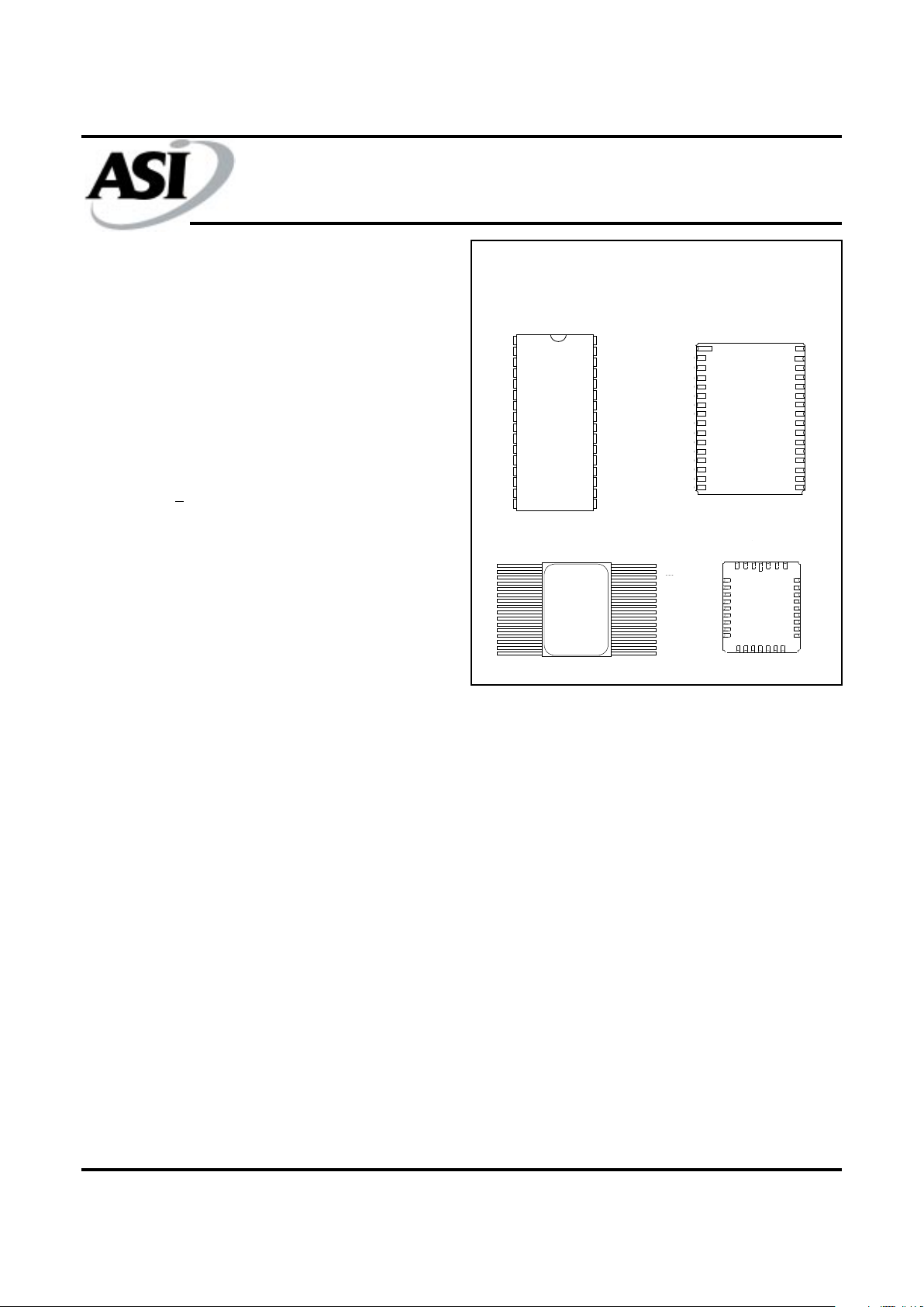
• Package(s)•
Ceramic DIP (400 mil) C No. 111
Ceramic DIP (600 mil) CW No. 112
Ceramic LCC EC No. 207
Ceramic LCC ECA No. 208
Ceramic Flatpack F No. 303
Ceramic SOJ DCJ No. 501
Ceramic SOJ SOJ No. 507
• 2V data retention/low power L
*Electrical characteristics identical to those provided for the 45ns
access devices.
PIN ASSIGNMENT
(Top View)
AVAILABLE AS MILITARY
SPECIFICATIONS
•SMD 5962-89598
•MIL-STD-883
NC 1 32
V
CC
A16 2 31 A15
A14 3 30 CE2
A12 4 29 WE\
A7 5 28 A13
A6 6 27 A8
A5 7 26 A9
A4 8 25 A11
A3 9 24 OE\
A2 10 23 A10
A1 11 22 CE\
A0 12 21 DQ8
DQ1 13 20 DQ7
DQ2 14 19 DQ6
DQ3 15 18 DQ5
V
SS
16 17 DQ4
NC 1 32
V
CC
A16 2 31 A15
A14 3 30 CE2
A12 4 29 WE\
A7 5 28 A13
A6 6 27 A8
A5 7 26 A9
A4 8 25 A11
A3 9 24 OE\
A2 10 23 A10
A1 11 22 CE\
A0 12 21 DQ8
DQ1 13 20 DQ7
DQ2 14 19 DQ6
DQ3 15 18 DQ5
V
SS
16 17 DQ4
NC 1 32
V
CC
A16 2 31 A15
A14 3 30 CE2
A12 4 29 WE\
A7 5 28 A13
A6 6 27 A8
A5 7 26 A9
A4 8 25 A11
A3 9 24 OE\
A2 10 23 A10
A1 11 22 CE\
A0 12 21 DQ8
DQ1 13 20 DQ7
DQ2 14 19 DQ6
DQ3 15 18 DQ5
V
SS
16 17 DQ4
32-Pin DIP (C, CW)
32-Pin SOJ (SOJ)
32-Pin LCC (EC)
32-Pin SOJ (DCJ)
32-Pin Flat Pack (F)
32-Pin LCC (ECA)
GENERAL DESCRIPTION
The MT5C1009 is a 1,048,576-bit high-speed CMOS
static RAM organized as 131,072 words by 8 bits. This device
uses 8 common input and output lines and has an output en-
able pin which operate faster than address access times during
READ cycle.
For design flexibility in high-speed memory
applications, this device offers chip enable (CE\) and output
enable (OE\) features. These enhancements can place the out-
puts in High-Z for additional flexibility in system design.
Writing to these devices is accomplished when write
enable (WE\) and CE\ inputs are both LOW . Reading is accom-
plished when WE\ remains HIGH and CE\ and OE\ go LOW.
The devices offer a reduced power standby mode when dis-
abled, allowing system designs to achieve low standby power
requirements.
The “L” version offers a 2V data retention mode, re-
ducing current consumption to 2mW maximum.
All devices operate from a single +5V power supply
and all inputs and outputs are fully TTL compatible. It is par-
ticularly well suited for use in high-density, high-speed system
applications.
128K x 8 SRAM
WITH CHIP & OUTPUT ENABLE
For more products and information
please visit our web site at
www.austinsemiconductor .com
4 3 2 1 32 31 30
A12
A14
A10
NC
V
CC
A15
CE2
14 15 16 17 18 19 20
DQ2
DQ3
V
SS
DQ4
DQ5
DQ6
DQ7
5
6
7
8
9
10
11
12
13
A7
A6
A5
A4
A3
A2
A1
A0
DQ1
29
28
27
26
25
24
23
22
21
WE
A13
A8
A9
A11
OE
A10
CE1
DQ8
\
\
\
6
NC
NC
NC
NC
SRAM
MT5C1009
Austin Semiconductor, Inc.
MT5C1009
Rev. 5.5 8/01
Austin Semiconductor, Inc. reserves the right to change products or specifications without notice.
2
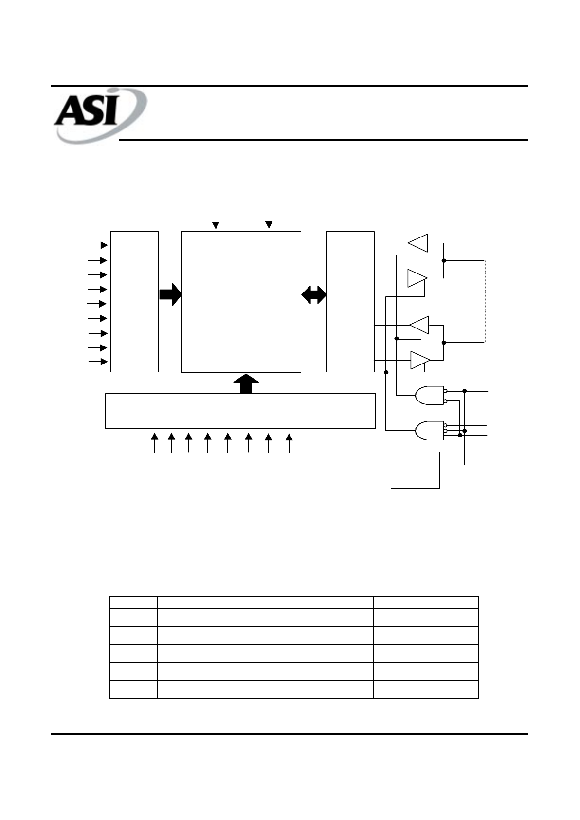
FUNCTIONAL BLOCK DIA GRAM
NOTE: The two least significant row address bits (A8 and A6) are encoded using gray code.
TRUTH TABLE
ROW DECODER
262,144-BIT
MEMORY ARRAY
I/O CONTROL
V
CC
GND
D
Q
8
D
Q
1
CE\
OE\
WE\
A
0
A
1
A
2
A
3
A
4
A
5
A
6
A
7
A
12
COLUMN DECODER
A
8
A
9
A
10
A
11
A
13
A
14
A
15
A
16
POWER
DOWN
CE\ WE\ OE\ MODE I/O PIN SUPPLY CURRENT
H X X Not Selected High-Z
I
SBT2
, I
SBC2
X X X Not Selected High-Z
I
SBT2
, I
SBC2
L H H Output Disable High-Z
I
CC
L H L Read
D
OUT
I
CC
L L X Write
D
IN
I
CC
SRAM
MT5C1009
Austin Semiconductor, Inc.
MT5C1009
Rev. 5.5 8/01
Austin Semiconductor, Inc. reserves the right to change products or specifications without notice.
3
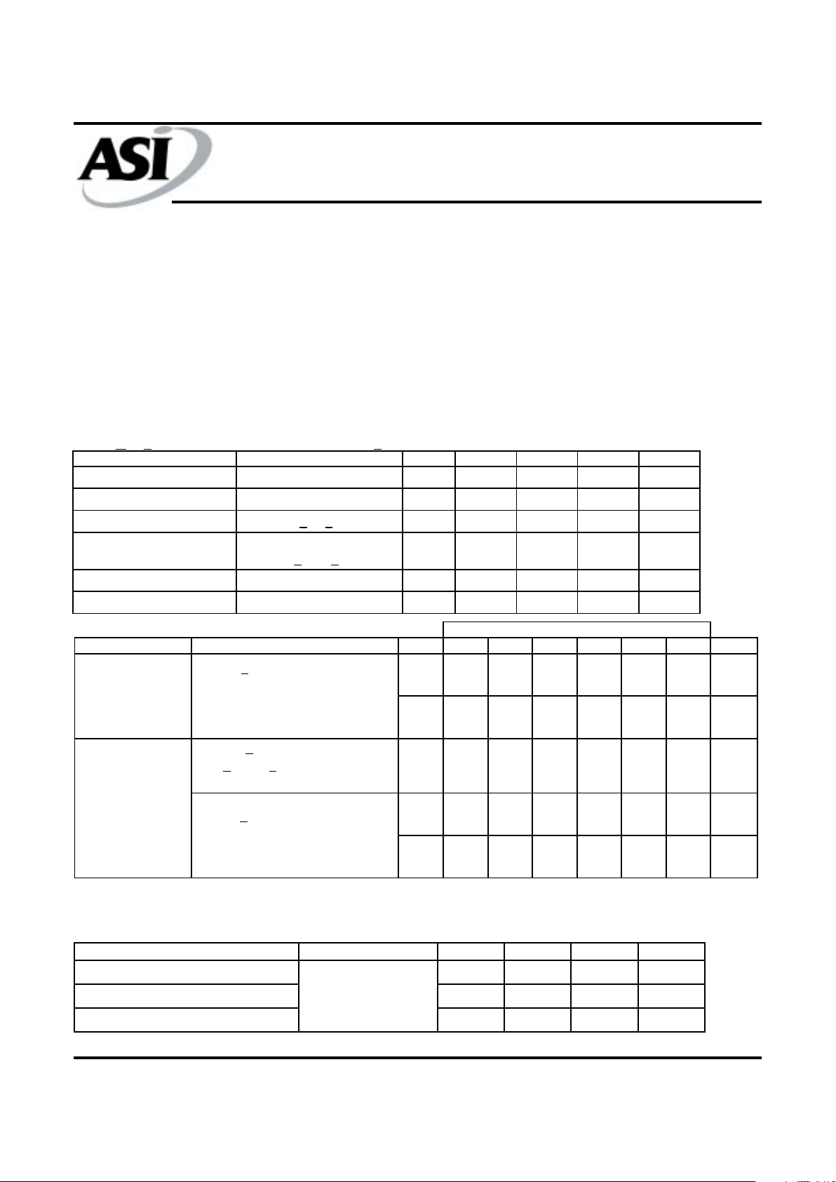
ABSOLUTE MAXIMUM RATINGS*
Supply Voltage Range (Vcc).............................-0.5V to +6.0V
Storage Temperature......................................-65°C to +150°C
Short Circuit Output Current (per I/O)….......................20mA
Voltage on any Pin Relative to Vss..................-0.5V to +7.0V
Max Junction T emperature**.......................................+150°C
Power Dissipation ...............................................................1 W
*Stresses at or greater than those listed under "Absolute Maxi-
mum Ratings" may cause permanent damage to the device.
This is a stress rating only and functional operation of the
device at these or any other conditions above those indicated
in the operation section of this specification is not implied.
Exposure to absolute maximum rating conditions for extended
periods will affect reliability. Refer to page 17 of this
datasheet for a technical note on this subject.
** Junction temperature depends upon package type, cycle
time, loading, ambient temperature and airflow, and humidity.
ELECTRICAL CHARACTERISTICS AND RECOMMENDED DC OPERATING CONDITIONS
(-55
o
C < T
C
< 125
o
C & -45
o
C to +85
o
C; V
CC
= 5.0V +10%)
CAPACITANCE
SYM -15 -20 -25 -35 -45 UNITS NOTES
I
CCSP
250 140 140 135 125 mA 3
I
CCLP
250 140 130 125 115 mA
Power Supply
Current: Standby
I
SBT
25 25 25 25 25 mA
I
SBCSP
10 10 10 10 10 mA
I
SBCLP
10 10 10 10 10 mA
MAX
CONDITIONS
CE\ >
V
CC
-0.2V; V
CC
= MAX
Inputs = V
IH
or V
IL
f = 0 Hz
PARAMETER
Power Supply
Current: Operating
CE\ <
V
IL
; OE\ = WE\ = V
IH
,
V
CC
= MAX, f = MAX = 1/t
RC
(MIN)
Output Open
(1)
L version only
CE\ >
V
IH
; All Other Inputs
<
V
IL
or > V
IH
, V
CC
= MAX
f = 0 Hz
DESCRIPTION CONDITIONS SYM MIN MAX UNITS NOTES
Input High (Logic 1) Voltage
V
IH
2.2
V
CC
+0.5
V1
Input Low (Logic 0) Voltage
V
IL
-0.5 0.8 V 1, 2
Input Leakage Current
0V<
V
IN
<V
CC
IL
I
-10 10 µA
Output Leakage Current
Output(s) disabled
0V<
V
OUT
<V
CC
IL
O
-10 10 µA
Output High Voltage
I
OH
=-4.0mA V
OH
2.4 V 1
Output Low Voltage
I
OL
=8.0mA V
OL
0.4 V 1
DESCRIPTION CONDITIONS SYM MAX UNITS NOTES
Input Capacitance (A0-A16)
C
I
12 pF 4
Output Capacitance
C
O
20 pF 4
Input Capacitance (CE\, WE\, OE\)
C
I
14 pF 4
T
A
= 25
o
C, f = 1MHz
V
CC
= 5V
SRAM
MT5C1009
Austin Semiconductor, Inc.
MT5C1009
Rev. 5.5 8/01
Austin Semiconductor, Inc. reserves the right to change products or specifications without notice.
4
ELECTRICAL CHARACTERISTICS AND RECOMMENDED AC OPERATING CONDITIONS
(Note 5) (-55
o
C < T
C
< 125
o
C & -40
o
C to +85
o
C; V
CC
= 5.0V +10%)
MIN M AX MIN MAX MIN MAX MIN MAX MIN MA X UNITS NOTES
READ CYCLE
READ cycle time
t
RC
15 20 25 35 45 ns
Address access time
t
AA
15 20 25 35 45 ns
Chip Enable access time
t
ACE
15 20 25 35 45 ns
Output hold from address change
t
OH
33333 ns
Chip Enable to output in Low-Z
t
LZCE
33333 ns4, 6, 7
Chip disable to output in High-Z
t
HZCE
7 8 10 15 20 ns 4, 6, 7
Output Enable access time
t
AOE
7 6 10 15 20 ns
Output Enable to output in Low-Z
t
LZOE
00000 ns4, 6, 7
Output disable to output in High-Z
t
HZOE
7 6 10 15 20 ns 4, 6, 7
WRITE CYCLE
WRITE cycle time
t
WC
15 20 25 35 45 ns
Chip Enable to end of write
t
CW
12 12 20 25 35 ns
Address valid to end of write
t
AW
12 12 20 25 35 ns
Address setup time
t
AS
00000 ns
Address hold from end of write
t
AH
00000 ns
WRITE pulse width (OE High)
t
WP
12 12 20 25 35 ns
Data setup time
t
DS
8 10152020 ns
Data hold time
t
DH
00000 ns
Write disable to output in Low-Z
t
LZWE
55555 ns4, 6, 7
Write Enable to output in High-Z
t
HZWE
7 9 10 15 20 ns 4, 6, 7
-25 -35 -45
DESCRIPTION
-15 -20
SYMBOL
SRAM
MT5C1009
Austin Semiconductor, Inc.
MT5C1009
Rev. 5.5 8/01
Austin Semiconductor, Inc. reserves the right to change products or specifications without notice.
5
AC TEST CONDITIONS
Input pulse levels ................................... Vss to 3.0V
Input rise and fall times ....................................... 5ns
Input timing reference levels ............................. 1.5V
Output reference levels ..................................... 1.5V
Output load .............................. See Figures 1 and 2
NOTES
1 . All voltages referenced to V
SS
(GND).
2 . -2V for pulse width < 20ns
3. I
CC
is dependent on output loading and cycle rates.
The specified value applies with the outputs
unloaded, and f = 1 Hz.
t
RC (MIN)
4. This parameter is guaranteed but not tested.
5. Test conditions as specified with the output loading
as shown in Fig. 1 unless otherwise noted.
6.
t
LZCE,
t
LZWE,
t
LZOE,
t
HZCE,
t
HZOE and
t
HZWE
are specified with CL = 5pF as in Fig. 2. Transition is
measured ±200mV typical from steady state voltage,
allowing for actual tester RC time constant.
7. At any given temperature and voltage condition,
t
HZCE is less than
t
LZCE, and
t
HZWE is less than
t
LZWE and
t
HZOE is less than
t
LZOE.
8. WE\ is HIGH for READ cycle.
9. Device is continuously selected. Chip enables and
output enables are held in their active state.
10. Address valid prior to, or coincident with, latest
occurring chip enable.
11.
t
RC = Read Cycle Time.
Fig. 1 Output Load
Equivalent
Fig. 2 Output Load
Equivalent
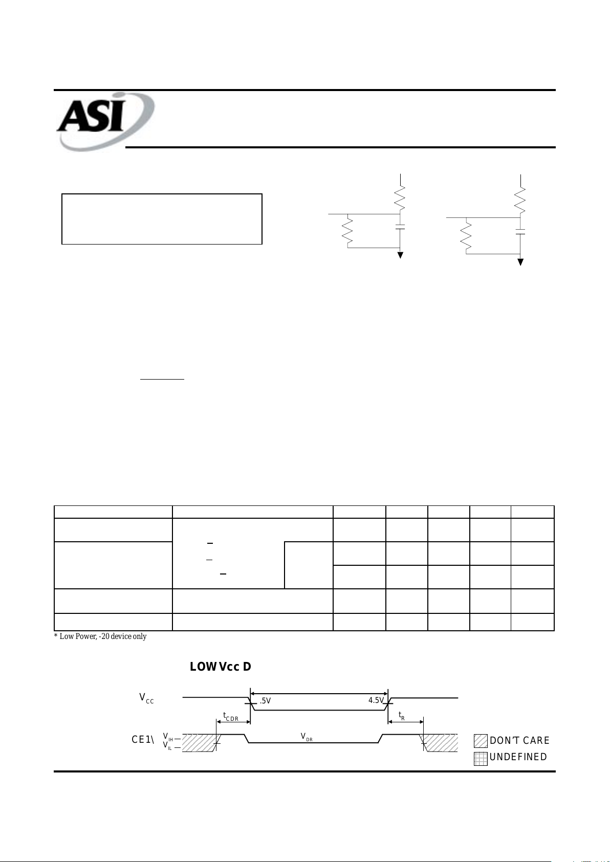
DATA RETENTION ELECTRICAL CHARACTERISTICS (L Version Only)
+5V
Q
255
30
480
5 pF
+5V
Q
255
480
2
3
2
3
1
23
4
1
23
4
1
23
4
1234
DON’T CARE
UNDEFINED
LOW Vcc DA T A RETENTION WA VEFORM
DESCRIPTION SYMBOL MIN MAX UNITS NOTES
V
CC
for Retention Data V
DR
2 --- V
I
CCDR1
*
0.75 mA
I
CCDR2
1.0 mA
Chip Deselect to Data
Retention Time
t
CDR
0 --- ns 4
Operation Recovery Time
t
R
t
RC
ns 4, 11
Data Retention Current
CE\ >
(V
CC
- 0.2V)
V
IN
> (V
CC
- 0.2V)
or <
0.2V
V
CC
= 2V
CONDITIONS
2
3
2
3
2
3
23
4
23
4
23
4
2
3
2
3
2
3
23
4
23
4
23
4
DA TA RETENTION MODE
V
DR
> 2V
4.5V
4.5V
V
DR
t
CDR
t
R
V
IH
V
IL
V
CC
CE1\
* Low Power, -20 device only
SRAM
MT5C1009
Austin Semiconductor, Inc.
MT5C1009
Rev. 5.5 8/01
Austin Semiconductor, Inc. reserves the right to change products or specifications without notice.
6
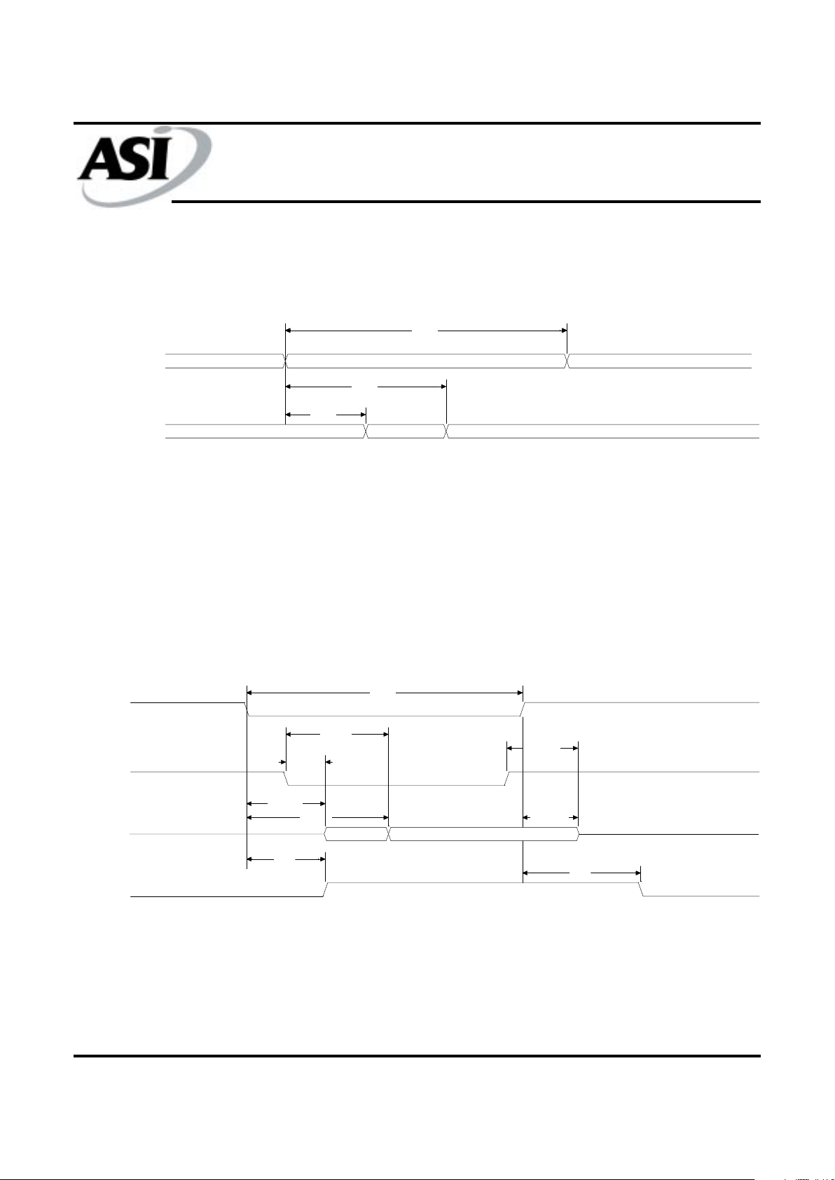
tAA
tOH
tRCtRC
PREVIOUS DATA VALID
VALID
DATA VALID
ADDRESS
DQ
tPD
tPU
tHZCEtACE
tLZCE
tHZOE
tLZOE
tAOE
tRCtRC
DATA VALID
CE\
OE\
DQ
Icc
READ CYCLE NO. 1
8, 9
READ CYCLE NO. 2
7, 8, 10, 12
t
RC
t
AA
t
OH
t
RC
t
AOE
t
LZOE
t
LZCE
t
ACE
t
PU
t
HZOE
t
HZCE
t
PD
 Loading...