

Datasheet ATmega603L-4AI, ATmega603L-4AC, ATmega603-6AI, ATmega603-6AC, ATmega103L-4AI Datasheet (ATMEL)
...Page 1
Features
•
Utilizes the AVR® Enhanced RISC Architecture
•
121 Powerful Instructions - Most Single Clock Cycle Execution
•
128K bytes of In-System Reprogrammable Flash ATmega103/L
64K bytes of In-System Reprogrammable Flash ATmega603/L
– SPI Interface for In-System Programming
– Endurance: 1,000 Write/Eras e Cycles
•
4K bytes EEPROM ATmega103/L
2K bytes of EEPROM ATmega603/L
– Endurance: 100,000 Write/Erase Cycles
•
4K bytes Internal SRAM
•
32 x 8 General Purpose Working Registers + Peripheral Control Registers
•
32 Programmable I/O Lines, 8 Output Lines, 8 Input Lines
•
Programmable Serial UART + SPI Serial Interface
•
V
Supply
CC
– 2.7 - 3.6V ATmega603L/ATmega103L
– 4.0 - 5.5V ATmega603/ATmega103
•
Fully Static Operation
– 0 - 6 MHz ATmega603/ATmega103
– 0 - 4 MHz ATmega603L/ATmega103L
•
Up to 6 MIPS Throughput at 6 MHz
•
RTC with Separate Oscillator
•
Two 8-Bit Timer/Counters with Separate Prescaler and PWM
•
One 16-Bit Timer/Counter with Separate Prescaler, Compare, Capture Modes and
Dual 8-, 9- or 10-Bit PWM
•
Programmable Watchdog Timer with On-Chip Oscillator
•
On-Chip Analog Comparator
•
8-Channel, 10-Bit ADC
•
Low Power Idle, Power Save and Power Down Modes
•
Software Selectable Clock Frequency
•
Programming Lock for Software Security
8-Bit
Microcontroller
with 64K/128K
Bytes In-System
Programmable
Flash
ATmega603
ATmega603L
ATmega103
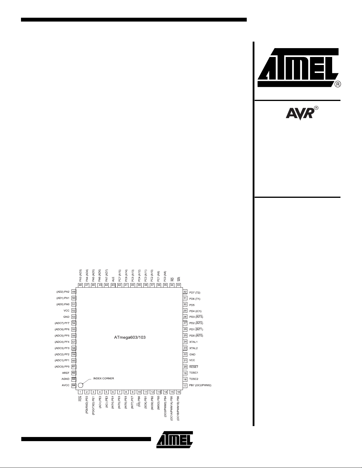
Pin Configuration
ATmega103L
TQFP
Preliminary
A Tmega103/L
A Tmega103/L
Rev. 0945BS–09/98
Note: This is a summ ary document. F or the co mplete 9 2
page document, please visit our web site at
www.atmel.com
and request literature #0945B.
or e-mail at
literature@atmel .com
1
Page 2
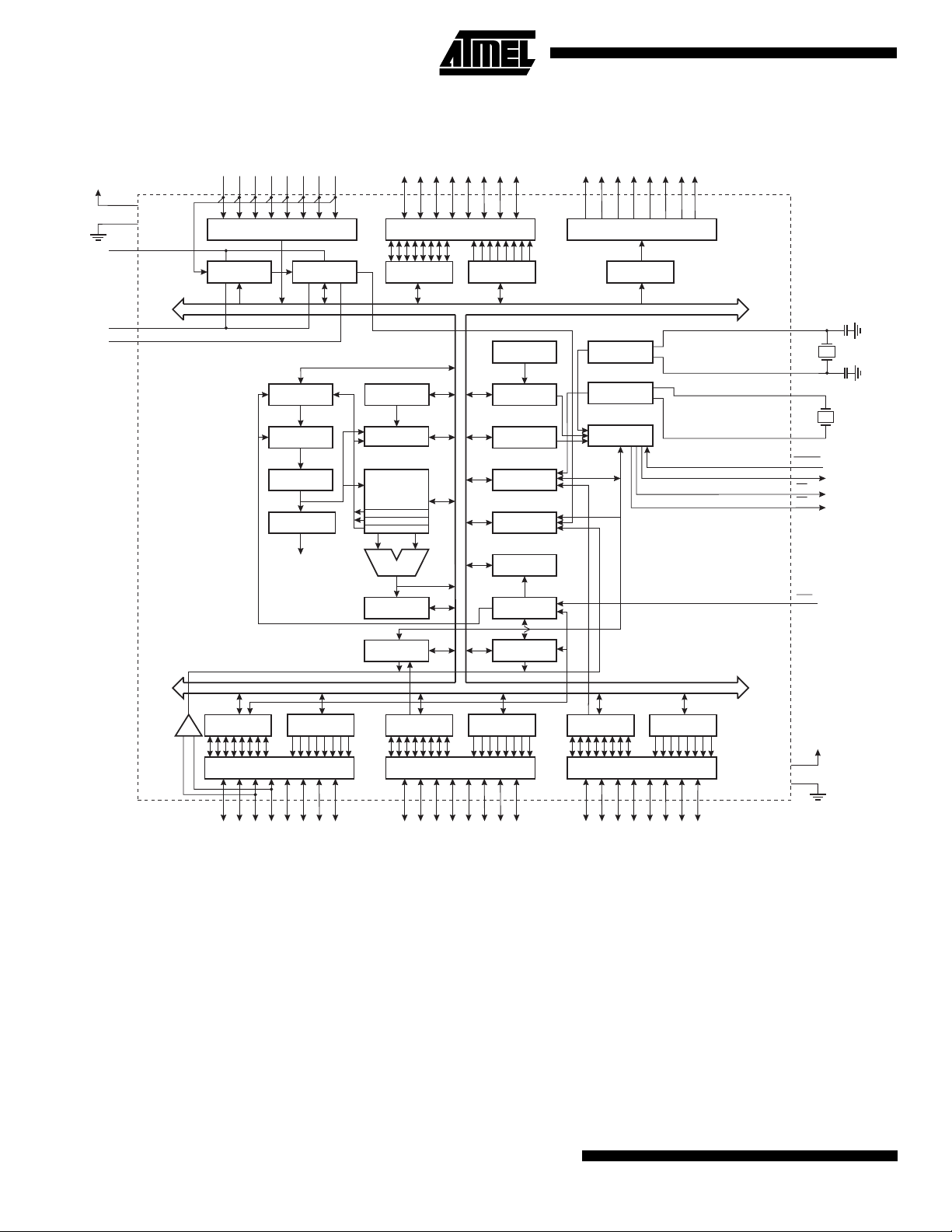
Block Diagram
Figure 1.
AVCC
AGND
AREF
The ATmega603/103 Block Diagram
VCC
GND
PORTF BUFFERS
ANALOG MUX ADC
PROGRAM
COUNTER
PROGRAM
FLASH
INSTRUCTION
REGISTER
INSTRUCTION
DECODER
CONTROL
LINES
PORTA DRIVER/BUFFERS
DATAREGISTER
PORTA
STACK
POINTER
SRAM
GENERAL
PURPOSE
REGISTERS
X
Y
Z
ALU
STATUS
REGISTER
PA0 - PA7PF0 - PF7
DATADIR.
REG. PORTA
INTERNAL
OSCILLATOR
WATCHDOG
MCU CONTROL
REGISTER
COUNTERS
INTERRUPT
EEPROM
PROGRAMMING
TIMER
TIMER/
UNIT
LOGIC
8-BIT DATA BUS
OSCILLATOR
OSCILLATOR
TIMING AND
PC0 - PC7
PORTC DRIVERS
DATAREGISTER
PORTC
CONTROL
XTAL1
XTAL1
TOSC2
TOSC1
RESET
ALE
WR
RD
PEN
SPI
ANALOG
COMPARATOR
DATAREGISTER
+
-
PORTE
DATADIR.
REG. PORTE
DATAREGISTER
PORTB
PORTB DRIVER/BUFFERSPORTE DRIVER/BUFFERS
PB0 - PB7PE0 - PE7
Description
The ATmega603/103 is a low-power CMOS 8-bit microcon-
AVR
troller based on the
executing powerful instructions in a single clock cycle, the
ATmega603/103 achieves th roughputs approaching 1
MIPS per MHz allowing the system designer to optimize
power consumption versus processing speed.
The AVR core is b ased o n an enh anced RISC ar chite ctur e
that combines a rich instruction set with 32 general purpose
working regist ers. All the 32 regi sters are directl y connected to the Arithmetic Logic Unit (ALU), allowing two
independent regist ers to be accessed in one single instruction executed in one c lock cycl e. The resu lting archite ctu re
enhanced RISC architecture. By
UART
DATADIR.
REG. PORTB
DATAREGISTER
PORTD
PORTD DRIVER/BUFFERS
PD0 - PD7
DATADIR.
REG. PORTD
VCC
GND
is more code efficient while achieving throughputs up to ten
times faster than conventional CISC microcontrollers.
The ATmega603/103 provides the following features:
64K/128K bytes of In-system Programmable Flash, 2K/4K
bytes EEPROM, 4K bytes SRAM , 32 general purpos e I/O
lines, 8 Input lines , 8 Output lines , 32 general pur pose
working registers, 4 flexible timer/counters with compare
modes and PWM, UART, programmable Watchdog Timer
with internal oscillator, an SPI serial port and three software
selectable pow er saving modes. T he Idle M ode sto ps the
CPU while allowing the SRAM, timer/counters, SPI port
and interrupt system to continue func tioning. The Power
2
ATmega603(L) and ATmega103(L)
Page 3
ATmega603(L) and ATmega103(L)
Down mode saves the register contents but freezes the
oscillator, disabling all other chip functions until the next
interrupt or hardware reset. In Power Save mode, the timer
oscillator continues to run, allowing the user to maintain a
timer base while the rest of the device is sleeping.
The device is manufactured using A tmel’s high-density
non-volatile memory technology. The on-chip ISP Flash
allows the program memory to be reprogrammed in-system
through a serial interface or by a co nventional non volatile
memory programmer. By combining an 8-bit RISC CPU
with a large array of ISP Flash on a monolithic chip, the
Atmel ATmega603/103 is a powerful microcontroller that
provides a h ighly flexibl e and cost effective solution to
many embedded control appl ic ati on s.
The ATmega603/103 AVR is supported with a full suite of
program and system development tools including: C compilers, macro assemblers, program debugger/simulators,
in-circuit emulators, and evaluation kits.
Comparison Between ATmega 603 and
ATmega 103
The ATmega603 h as 64K bytes o f In-Sys tem Pro gramm able Flash, 2K bytes o f EEPROM, an d 4K bytes o f internal
SRAM. The ATmega603 does not have the ELPM instruction.
The ATmega103 has 128K bytes of In-System Programmable Flash, 4K bytes of EEPROM, and 4K bytes of internal SRAM. The ATmega10 3 has the ELPM instruct ion,
necessary to reach the upper half of the Flash memory for
constant table lookup.
Table 1 summarizes the dif ferent memory size s for the two
devices.
Table 1.
Part Flash EEPROM SRAM
ATmega603 64K bytes 2K bytes 4K bytes
ATmega103 128K bytes 4K bytes 4K bytes
Memory Size Summary
Pin Descriptions
VCC
Supply voltage
GND
Ground
Port A (PA7..PA0)
Port A is an 8-bit bi-directional I/O port. Port pins can provide internal pull-up resistors (selected for each bit). The
Port A output buffers can sink 20 mA and can drive LED
displays directly. When pins PA0 to PA7 are used as inputs
and are externally pull ed low, they will source c urrent if the
internal pull-up resistors are activated.
Port A serves as Multiplexed Address/Data bus when using
external SRAM.
Port B (PB7..PB0)
Port B is an 8-bi t b i-di r ect ion al I/O pin s wit h i nte rn al pu ll -up
resistors. The Port B output buffers can sink 20 mA. As
inputs, Port B pins that are externally pulled low, will source
current if the pull-up resistors are activated.
Port B also serves the functions of various special features.
Port C (PC7..PC0)
Port C is an 8- bi t Outp ut port . The Port C out put buf fer s can
sink 20 mA.
Port C also serv es as Ad dress ou tput wh en using extern al
SRAM.
Port D (PD7..PD0)
Port D is an 8-bit bi-directional I/O port with internal pull-up
resistors. The Port D output buffers can sink 20 mA. As
inputs, Port D pins that are external ly pul le d low will s our ce
current if the pull-up resistors are activated.
Port D also serves the functions of various special features.
Port E (PE7..PE0)
Port E is an 8-bit bi- directi onal I/O port with internal pull -up
resistors. The Port E output buffers can sink 20 mA. As
inputs, Port E pins t hat a re ex ter na lly p ull ed l ow w il l sour ce
current if the pull-up resistors are activated.
Port E also serves the functions of various special features.
Port F (PF7..PF0)
Port F is an 8-bi t Input port. P ort F al so serv es as the a nalog inputs for the ADC.
RESET
input. A low on this pin for two machine cy cles while the
oscillator is running resets the device.
XTAL1
Input to the inverting os cillator ampli fier and input to th e
internal clock operating circuit.
XTAL2
Output from the inverting oscillator amplifier
TOSC1
Input to the inverting Timer/Counter oscillator amplifier
TOSC2
Output from the inverting Timer/Counter oscillator amplifier
WR
External SRAM Write Strobe.
RD
External SRAM Read Strobe.
ALE
ALE is the Address Latch Enable used when the Ex ternal
Memory is enabled. The ALE strob e is used to latch the
low-order address (8 bits) into an address latch during the
3
Page 4

first access cycl e, and the A D0-7 pins ar e used for data
during the second access cycle.
AV
CC
This is the supply voltage to the A/D Converter. It should be
externally connec ted to V
via a low-pass filter. See
CC
page 53 for details on operation of the ADC.
AREF
This is the analog reference input for the ADC converter.
For ADC operations, a voltage in the range AGND to AVCC
must be applied to this pin.
AGND
If the board has a sepa rate analog gr ound plane, th is pin
should be co nnect ed to this gr ound plane . Ot herwi se, connect to GND.
PEN
This is a programming enabl e pin for the low -voltage ser ial
programming mode. By holding this pin low during a poweron reset, the device will enter the serial programming
mode.
Crystal Oscillator
XTAL1 and XTAL2 are input and output, respectively, of an
inverting amplifier which can be configured for use as an
on-chip oscillator, as shown in Figure 2. Either a quartz
crystal or a ceramic resonator may be used. To drive the
device from an external clock source, XTAL2 should be left
unconnected while XTAL1 is driven as shown in Figure 3.
For the Timer Oscillator pins, O SC1 an d OSC2, t he cr ystal
is connected directly be twee n the pi ns . No ex ternal cap ac itors are needed. The oscillator is optimi zed for use with a
32,768Hz watch crys tal. A n e xt er nal cloc k sign al app li ed t o
this pin goes throug h the same a mplifier having a bandwidth of 256kHz. The external clock signal should therefore
be in the interval 0Hz - 256kHz.
Figure 2.
Oscillator Connec tion s
C2
XTAL2
C1
XTAL1
Figure 3.
External Clock Drive Configuration
NC
EXTERNAL
OSCILLATOR
SIGNAL
XTAL2
XTAL1
GND
AT mega603/103 Architectural Overview
The fast-access register file contains 32 x 8-bit general purpose working registers with a single clock cycle access
time. This means that during one single clock cycle, one
ALU (Arithmetic Logic Unit) operation is executed. Two
operands are output from the register file, the operation is
executed, and the result is stored back in the register file in one clock cycle.
Six of the 32 registers can be used as three 16-bit indirect
address register pointers for Data Space addressing enabling efficient address calculati ons. One of the three
address pointers is also used as the address pointer for the
constant table look up function. These added function registers are the 16-bit X-register, Y-register and Z-register.
The ALU supports arithmetic and logic functions b etween
registers or between a const ant and a r egist er. Si ngle re gister operations are also executed in the ALU. Figure 4
shows the ATmega603/103 AVR Enhanced RISC microcontroller architectu re .
In addition to the register operation, the conventional memory addressi ng mode s can be us ed on th e regi ster fil e as
well. This is e nabled by th e fact that t he register fil e is
assigned the 32 lowermost Data Space addresses, allowing them to be accessed as thou gh they were ordinary
memory locations.
The I/O memory space contains 64 addresse s for CPU
peripheral functions as Control Registers, Timer/Counters,
A/D-converters, an d other I/O func tions. The I/O M emory
can be accessed dir ectly, or as the Da ta Space loca tions
following those of the register file, $20 - $5F.
GND
4
ATmega603(L) and ATmega103(L)
Page 5

ATmega603(L) and ATmega103(L)
Figure 4.
The ATmega603/103 AVR Enhanced RISC Architecture
AVR ATmega603/103 Architecture
32K/64K x 16
Program
Memory
Instruction
Register
Instruction
Decoder
Control Lines
Program
Counter
DirectAddressing
IndirectAddressing
Data Bus 8-bit
Status
and Test
32 x 8
General
Purpose
Registers
Peripherals
ALU
4K x 8
Data
SRAM
The AVR uses a Ha rvard archi tecture concep t - with separate memories and buses for prog ram and data. The program memory is executed with a single level pipelining.
While one instruction is being executed, the next instruction
is pre-fetched from the program memory. T his concept
enables instructions to be executed in every clock cycle.
The program memory is in-system programmable Flash
memory. With a few exceptions, AVR instructions have a
single 16-bit w ord format, me aning that ev ery program
memory address contains a single 16-bit instruction.
During interrupts a nd subr outine cal ls, the re turn addre ss
program counter (PC) is stored on the s tack. The stack is
effectively allocat ed in the g enera l data SRAM, a nd cons equently the stack size is only limited by the total SRAM size
and the usage of the SRA M. Al l us er pro gr ams mu st i nit ia lize the SP in the reset routine (before subroutines or interrupts are execute d). The 16-bit stack pointer SP is
read/write accessib le in the I/O spac e.
2K/4K x 8
EEPROM
The 4000 bytes data SRAM can be easily accessed
through the five different addressing modes supported in
the AVR architecture.
A flexible interrupt module has its control registers in the
I/O space with an additional global interrupt enable bit in
the status reg ister. All th e diffe rent int errupt s have a sepa rate interr upt vector i n the inter rupt vector table at the
beginning of the program memory. The different interrupts
have priority in accordance with their interrupt vector position. The lower the interrupt vector address, the higher the
priority.
The memory spaces in the AVR architecture are all l inear
and regular memory maps.
The General Purpose Register File
Figure 5 shows the structure of the 32 general purpose
working registers in the CPU.
5
Page 6

ATmega603/103 Register Summary
Address Name Bit7 Bit6 Bit5 Bit4 Bit3 Bit2 Bit1 Bit0 Page
$3F ($5F) SREG I T H S V N Z C page14
$3E ($5E) SPH SP15 SP14 SP13 SP12 SP11 SP10 SP9 SP8 page 14
$3D ($5D) SPL SP7 SP6 SP5 SP4 SP3 SP2 SP1 SP0 page 14
$3C ($5C) XDIV XDIVEN XDIV6 XDIV5 XDIV4 XDIV3 XDIV2 XDIV1 XDIV0 page 16
$3B ($5B) RAMPZ - - - - - - - RAMPZ0 page 15
$3A ($5A) EICR ISC71 ISC70 ISC6 1 ISC60 ISC51 ISC50 ISC41 ISC40 page 23
$39 ($59) EIMSK INT7 INT6 INT5 INT4 INT3 INT2 INT1 INT0 page 22
$38 ($58) EIFR INTF7 INTF6 INTF5 INTF4 - - - - page 22
$37 ($57) TIMSK OCIE2 TOIE2 TICIE1 OCIE1A OCIE1B TOIE1 OCIE0 TOIE0 page 23
$36 ($56) TIFR OCF2 TOV2 ICF1 OCF1A OCF1B TOV1 OCF0 TOV0 page 24
$35 ($55) MCUCR SRE SRW SE SM1 SM0 - - - page 15
$34 ($54) MCUSR - - - - - - EXTRF PORF page21
$33 ($53) TCCR0 - PWM0 COM01 COM00 CTC0 CS02 CS01 CS00 page 28
$32 ($52) TCNT0 Timer/Counter0 (8 Bit) page 30
$31 ($51) OCR0 Timer/Counter0 Output Compare Register page 30
$30 ($50) ASSR - - - - AS0 TCN0UB OCR0UB TCR0UB page 32
$2F ($4F) TCCR1A COM1A1 COM1A0 COM1B1 COM1B0 - - PWM11 PWM10 page 34
$2E ($4E) TCCR1B ICNC1 ICES1 - - CTC1 CS12 CS11 CS10 page 37
$2D ($4D) TCNT1H Timer/Counter1 - Counter Register High Byte page 36
$2C ($4C) TCNT1L Timer/Counter1 - Counter Register Low Byte page 36
$2B ($4B) OCR1AH Timer/Counter1 - Output Compare Register A High Byte page 37
$2A ($4A) OCR1AL Timer/Counter1 - Output Compare Register A Low Byte page 37
$29 ($49) OCR1BH Timer/Counter1 - Output Compare Register B High Byte page 37
$28 ($48) OCR1BL Timer/Counter1 - Output Compare Register B Low Byte page 37
$27 ($47) ICR1H Timer/Counter1 - Input Capture Register High Byte page 37
$26 ($46) ICR1L Timer/Counter1 - Input Capture Register Low Byte page 37
$25 ($45) TCCR2 - PWM2 COM21 COM20 CTC2 CS22 CS21 CS20 page28
$24 ($44) TCNT2 Timer/Counter2 (8 Bit) page 30
$23 ($43) OCR2 Timer/Counter2 Output Compare Register page 30
$21 ($47) WDTCR
$1F ($3F) EEARH
$1E ($3E) EEARL EEPROM Address Register L page 41
$1D ($3D) EEDR EEPROM Data Register page 41
$1C ($3C) EECR - - - - EERIE EEMWE EEWE EERE page 41
$1B ($3B) PORTA PORTA7 PORTA6 PORTA5 PORTA4 PORTA3 PORTA2 PORTA1 PORTA0 page 57
$1A ($3A) DD RA DDA7 DDA6 DDA5 DDA4 DDA3 DDA2 DDA1 DDA0 page 57
$19 ($39) PINA PINA7 PINA6 PINA5 PINA4 PINA3 PINA2 PINA1 PINA0 page 57
$18 ($38) PORTB PORTB7 PORTB6 PORTB5 PORTB4 PORTB3 PORTB2 PORTB1 PORTB0 page 59
$17 ($37) DDRB DDB7 DDB6 DDB5 DDB4 DDB3 DDB2 DDB1 DDB0 page 59
$16 ($36) PINB PINB7 PINB6 PINB5 PINB4 PINB3 PINB2 PINB1 PINB0 page 59
$15 ($35) PORTC PORTC7 PORTC6 PORTC5 PORTC4 PORTC3 PORTC2 PORTC1 PORTC0 page 65
$12 ($32) PORTD PORTD7 PORTD6 PORTD5 PORTD4 PORTD3 PORTD2 PORTD1 PORTD0 page 66
$11 ($31) DDRD DDD7 DDD6 DDD5 DDD4 DDD3 DDD2 DDD1 DDD0 page 66
$10 ($30) PIND PIND7 PIND6 PIND5 PIND4 PIND3 PIND2 PIND1 PIND0 page 66
$0F ($2F) SPDR SPI Data Register page 46
$0E ($2E) SPSR SPIF WCOL - - - - - - page 46
$0D ($2D) SPCR SPIE SPE DORD MSTR CPOL CPHA SPR1 SPR0 page 45
$0C ($2C) UDR UART I/O Data Register page 49
$0B ($2B) USR RXC TXC UDRE FE OR - - - page 49
$0A ($2A) UCR RXCIE TXCIE UDRIE RXEN TXEN CHR9 RXB8 TXB8 page 50
$09 ($29) UBRR UART Baud Rate Register page 51
$08 ($28) ACSR ACD - ACO ACI ACIE ACIC ACIS1 ACIS0 page 52
$07 ($27) ADMUX - - - - - MUX2 MUX1 MUX0 page 54
$06 ($26) ADCSR ADES ABSY ADRF ADIF A DIE ADPS2 ADPS1 ADPS0 page 54
$05 ($25) ADCH - - - - - - ADC9 ADC8 page 55
$04 ($24) ADCL ADC7 ADC6 ADC5 ADC4 ADC3 ADC2 ADC1 ADC0 page 55
$03 ($23) PORTE PORTE7 PORTE6 PORTE5 PORTE4 PORTE3 PORTE2 PORTE1 PORTE0 page 69
$02 ($22) DDRE DDE7 DDE6 DDE5 DDE4 DDE3 DDE2 DDE1 DDE0 page 69
$01 ($21) PINE PINE7 PINE6 PINE5 PINE4 PINE3 PINE2 PINE1 PINE0 page 69
$00 ($20) PINF PINF7 PINF6 PINF5 PINF4 PINF3 PINF2 PINF1 PINF0 page 73
-
-
- - WDTOE WDE WDP2 WDP1 WDP0 page 40
- - - EEAR11 EEAR10 EEAR9 EEAR8 page 41
6
ATmega603(L) and ATmega103(L)
Page 7

ATmega603(L) and ATmega103(L)
ATmega603/103 Instruction Set Summary
Mnemonics Operands Description Operation Flags #Clocks
ARITHMETIC AND LOGIC INSTRUCTIONS
ADD Rd, Rr Add two Registers Rd ← Rd + Rr Z,C,N,V,H 1
ADC Rd, Rr Add with Carry two Registers Rd ← Rd + Rr + C Z,C,N,V,H 1
ADIW Rdl,K Add Immediate to Word Rdh:Rdl ← Rdh:Rdl + K Z,C,N,V,S 2
SUB Rd, Rr Subtract two Registers Rd ← Rd - Rr Z,C,N,V,H 1
SUBI Rd, K Subtract Constant from Register Rd ← Rd - K Z,C,N,V,H 1
SBC Rd, Rr Subtract with Carry two Registers Rd ← Rd - Rr - C Z,C,N,V,H 1
SBCI Rd, K Subtract with Carry Constant from Reg. Rd ← Rd - K - C Z,C,N,V,H 1
SBIW Rdl,K Subtract Immediate from Word Rdh:Rdl ← Rdh:Rdl - K Z,C,N,V,S 2
AND Rd, Rr Logical AND Registers Rd ← Rd • Rr Z,N,V 1
ANDI Rd, K Logical AND Register and Constant Rd ← Rd • K Z,N,V 1
OR Rd, Rr Logical OR Registers Rd ← Rd v Rr Z,N,V 1
ORI Rd, K Logical OR Register and Constant Rd ← Rd v K Z,N,V 1
EOR Rd, Rr Exclusive OR Registers Rd ← Rd ⊕ Rr Z,N,V 1
COM Rd One’s Complement Rd ← $FF - Rd Z,C,N,V 1
NEG Rd Two’s Complement Rd ← $00 - Rd Z,C,N,V,H 1
SBR Rd,K Set Bit(s) in Register Rd ← Rd v K Z,N,V 1
CBR Rd,K Clear Bit(s) in Register Rd ← Rd • ($FF - K) Z,N,V 1
INC Rd Increment Rd ← Rd + 1 Z,N,V 1
DEC Rd Decrement Rd ← Rd - 1 Z,N,V 1
TST Rd Test for Zero or Minus Rd ← Rd • Rd Z,N,V 1
CLR Rd Clear Register Rd ← Rd ⊕ Rd Z,N,V 1
SER Rd Set Register Rd ← $FF None 1
BRANCH INSTRUCTIONS
RJMP k Relative Jump PC ← PC + k + 1 None 2
IJMP Indirect Jump to (Z) PC ← Z None 2
JMP k Direct Jump PC ← kNone3
RCALL k Relative Subroutine Call PC ← PC + k + 1 None 3
ICALL Indirect Call to (Z) PC ← ZNone3
CALL k Direct Subroutine Call PC ← kNone4
RET Subroutine Return PC ← STACK None 4
RETI Interrupt Return PC ← STACK I 4
CPSE Rd,Rr Compare, Skip if Equal if (Rd = Rr) PC ← PC + 2 or 3 None 1 / 2
CP Rd,Rr Compare Rd - Rr Z, N,V,C,H 1
CPC Rd,Rr Compare with Carry Rd - Rr - C Z, N,V,C,H 1
CPI Rd,K Compare Register with Immediate Rd - K Z, N,V,C,H 1
SBRC Rr, b Skip if Bit in Register Cleared if (Rr(b)=0) PC ← PC + 2 or 3 None 1 / 2
SBRS Rr, b Skip if Bit in Register is Set if (Rr(b)=1) PC ← PC + 2 or 3 None 1 / 2
SBIC P, b Skip if Bit in I/O Register Cleared if (P(b)=0) PC ← PC + 2 or 3 None 1 / 2
SBIS P, b Skip if Bit in I/O Register is Set if (P(b)=1) PC ← PC + 2 or 3 None 1 / 2
BRBS s, k Branch if Status Flag Set if (SREG(s) = 1) then PC←PC+k + 1 None 1 / 2
BRBC s, k Branch if Status Flag Cleared if (SREG(s) = 0) then PC←PC+k + 1 None 1 / 2
BREQ k Branch if Equal if (Z = 1) then PC ← PC + k + 1 None 1 / 2
BRNE k Branch if Not Equal if (Z = 0) then PC ← PC + k + 1 None 1 / 2
BRCS k Branch if Carry Set if (C = 1) then PC ← PC + k + 1 None 1 / 2
BRCC k Branch if Carry Cleared if (C = 0) then PC ← PC + k + 1 None 1 / 2
BRSH k Branch if Same or Higher if (C = 0) then PC ← PC + k + 1 None 1 / 2
BRLO k Branch if Lower if (C = 1) then PC ← PC + k + 1 None 1 / 2
BRMI k Branch if Minus if (N = 1) then PC ← PC + k + 1 None 1 / 2
BRPL k Branch if Plus if (N = 0) then PC ← PC + k + 1 None 1 / 2
BRGE k Branch if Greater or Equal, Signed if (N ⊕ V= 0) then PC ← PC + k + 1 None 1 / 2
BRLT k Branch if Less Than Zero, Signed if (N ⊕ V= 1) then PC ← PC + k + 1 None 1 / 2
BRHS k Branch if Half Carry Flag Set if (H = 1) then PC ← PC + k + 1 None 1 / 2
BRHC k Branch if Half Carry Flag Cleared if (H = 0) then PC ← PC + k + 1 None 1 / 2
BRTS k Branch if T Flag Set if (T = 1) then PC ← PC + k + 1 None 1 / 2
BRTC k Branch if T Flag Cleared if (T = 0) then PC ← PC + k + 1 None 1 / 2
BRVS k Branch if Overflow Flag is Set if (V = 1) then PC ← PC + k + 1 None 1 / 2
BRVC k Branch if Overflow Flag is Cleared if (V = 0) then PC ← PC + k + 1 None 1 / 2
BRIE k Branch if Interrupt Enabled if ( I = 1) then PC ← PC + k + 1 None 1 / 2
BRID k Branch if Interrupt Disabled if ( I = 0) then PC ← PC + k + 1 None 1 / 2
7
Page 8

ATmega603/103 Instruction Set Summary (Continued)
DATA TRANSFER INSTRUCTIONS
()
ELPM
MOV Rd, Rr Move Between Registers Rd ← Rr None 1
LDI Rd, K Load Immediate Rd ← K None 1
LD Rd, X Load Indirect Rd ← (X) None 2
LD Rd, X+ Load Indirect and Post-Inc. Rd ← (X), X ← X + 1 None 2
LD Rd, - X Load Indirect and Pre-Dec. X ← X - 1, Rd ← (X) None 2
LD Rd, Y Load Indirect Rd ← (Y) None 2
LD Rd, Y+ Load Indirect and Post-Inc. Rd ← (Y), Y ← Y + 1 None 2
LD Rd, - Y Load Indirect and Pre-Dec. Y ← Y - 1, Rd ← (Y) None 2
LDD Rd,Y+q Load Indirect with Displacement Rd ← (Y + q) None 2
LD Rd, Z Load Indirect Rd ← (Z) None 2
LD Rd, Z+ Load Indirect and Post-Inc. Rd ← (Z), Z ← Z+1 None 2
LD Rd, -Z Load Indirect and Pre-Dec. Z ← Z - 1, Rd ← (Z) None 2
LDD Rd, Z+q Load Indirect with Displacement Rd ← (Z + q) None 2
LDS Rd, k Load Direct from SRAM Rd ← (k) None 2
ST X, Rr Store Indirect (X) ← Rr None 2
ST X+, Rr Store Indirect and Post-Inc. (X) ← Rr, X ← X + 1 None 2
ST - X, Rr Store Indirect and Pre-Dec. X ← X - 1, (X) ← Rr None 2
ST Y, Rr Store Indirect (Y) ← Rr None 2
ST Y+, Rr Store Indirect and Post-Inc. (Y) ← Rr, Y ← Y + 1 None 2
ST - Y, Rr Store Indirect and Pre-Dec. Y ← Y - 1, (Y) ← Rr None 2
STD Y+q,Rr Store Indirect with Displacement (Y + q) ← Rr None 2
ST Z, Rr Store Indirect (Z) ← Rr None 2
ST Z+, Rr Store Indirect and Post-Inc. (Z) ← Rr, Z ← Z + 1 None 2
ST -Z, Rr Store Indirect and Pre-Dec. Z ← Z - 1, (Z) ← Rr None 2
STD Z+q,Rr Store Indirect with Displacement (Z + q) ← Rr None 2
STS k, Rr Store Direct to SRAM (k) ← Rr None 2
LPM Load Program Memory R0 ← (Z) None 3
IN Rd, P In Port Rd ← P None 1
OUT P, Rr Out Port P ← Rr None 1
PUSH Rr Push Register on Stack STACK ← Rr None 2
POP Rd Pop Register from Stack Rd ← STACK None 2
BIT AND BIT-TEST INSTRUCTIONS
SBI P,b Set Bit in I/O Register I/O(P,b) ← 1 None 2
CBI P,b Clear Bit in I/O Register I/O(P,b) ← 0 None 2
LSL Rd Logical Shift Left Rd(n+1) ← Rd(n), Rd(0) ← 0 Z,C,N,V 1
LSR Rd Logical Shift Right Rd(n) ← Rd(n+1), Rd(7) ← 0 Z,C,N,V 1
ROL Rd Rotate Left Through Carry Rd(0)←C,Rd(n+1)← Rd(n),C←Rd(7) Z,C,N,V 1
ROR Rd Rotate Right Through Carry Rd(7)←C,Rd(n)← Rd(n+1),C←Rd(0) Z,C,N,V 1
ASR Rd Arithmetic Shift Right Rd(n) ← Rd(n+1), n=0..6 Z,C,N,V 1
SWAP Rd Swap Nibbles Rd(3..0)←Rd(7..4),Rd(7..4)←Rd(3..0) None 1
BSET s Flag Set SREG(s) ← 1 SREG(s) 1
BCLR s Flag Clear SREG(s) ← 0 SREG(s) 1
BST Rr, b Bit Store from Register to T T ← Rr(b) T 1
BLD Rd, b Bit load from T to Register Rd(b) ← T None 1
SEC Set Carry C ← 1C1
CLC Clear Carry C ← 0 C 1
SEN Set Negative Flag N ← 1N1
CLN Clear Negative Flag N ← 0 N 1
SEZ Set Zero Flag Z ← 1Z1
CLZ Clear Zero Flag Z ← 0 Z 1
SEI Global Interrupt Enable I ← 1I1
CLI Global Interrupt Disable I ← 0 I 1
SES Set Signed Test Flag S ← 1S1
CLS Clear Signed Test Flag S ← 0 S 1
SEV Set Twos Complement Overflow. V ← 1V1
CLV Clear Twos Complement Overflow V ← 0 V 1
SET Set T in SREG T ← 1T1
CLT Clear T in SREG T ← 0 T 1
SEH Set Half Carry Flag in SREG H ← 1H1
CLH Clear Half Carry Flag in SREG H ← 0 H 1
NOP No Operation None 1
SLEEP Sleep (see specific descr. for Sleep function) None 3
WDR Watchdog Reset (see specific descr. for WD timer) None 1
Extended Load Program Memory R0 ← (Z+RAMPZ) None 3
8
ATmega603(L) and ATmega103(L)
Page 9

ATmega603(L) and ATmega103(L)
Ordering Information
Speed (MHz) Power Supply Ordering Code Package Operation Range
4 2.7 - 3.6V ATmega603L-4AC 64A Commercial
(0°C to 70°C)
ATmega603L-4AI 64A Industrial
(-40°C to 85°C)
6 4.0 - 5.5V ATmega603-6AC 64A Commercial
(0°C to 70°C)
ATmega603-6AI 64A Industrial
(-40°C to 85°C)
4 2.7 - 3.6V ATmega103L-4AC 64A Commercial
(0°C to 70°C)
ATmega103L-4AI 64A Industrial
(-40°C to 85°C)
6 4.0 - 5.5V ATmega103-6AC 64A Commercial
(0°C to 70°C)
ATmega103-6AI 64A Industrial
(-40°C to 85°C)
Package Type
64A 64-Lead, Thin (1.0 mm) Plastic Gull Wing Quad Flat Package (TQFP)
9
Page 10

Packaging Information
64A
, 64-Lead, Thin (1.0 mm) Plastic Gull Wing Quad
Flat Package (TQFP)
Dimensions in Millimeters and (Inches)*
PIN 1 ID
0.80(0.031) BSC
0.20(0.008)
0.10(0.004)
16.25(0.640)
15.75(0.620)
14.10(0.555)
13.90(0.547)
0-7
0.75(0.030)
0.45(0.018)
SQ
SQ
*Controlling dimension: millimeters
0.45(0.018)
0.30(0.012)
1.20 (.047) MAX
0.15(0.006)
0.05(0.002 )
10
ATmega603(L) and ATmega103(L)
 Loading...