

Atmel ATmega48/V, ATmega88/V, ATmega168/V Datasheet

Features
• High Performance, Low Power AVR
• Advanced RISC Architecture
– 131 Powerful Instructions – Most Single Clock Cycle Execution
– 32 x 8 General Purpose Working Registers
– Fully Static Operation
– Up to 20 MIPS Throughput at 20 MHz
– On-chip 2-cycle Multiplier
• High Endurance Non-volatile Memory segments
– 4/8/16K Bytes of In-System Self-programmable Flash program memory
– 256/512/512 Bytes EEPROM
– 512/1K/1K Bytes Internal SRAM
– Write/Erase cyles: 10,000 Flash/100,000 EEPROM
– Data retention: 20 years at 85°C/100 years at 25°C
– Optional Boot Code Section with Independent Lock Bits
In-System Programming by On-chip Boot Program
True Read-While-Write Operation
– Programming Lock for Software Security
• Peripheral Features
– Two 8-bit Timer/Counters with Separate Prescaler and Compare Mode
– One 16-bit Timer/Counter with Separate Prescaler, Compare Mode, and Capture Mode
– Real Time Counter with Separate Oscillator
– Six PWM Channels
– 8-channel 10-bit ADC in TQFP and QFN/MLF package
– 6-channel 10-bit ADC in PDIP Package
– Programmable Serial USART
– Master/Slave SPI Serial Interface
– Byte-oriented 2-wire Serial Interface (Philips I
– Programmable Watchdog Timer with Separate On-chip Oscillator
– On-chip Analog Comparator
– Interrupt and Wake-up on Pin Change
• Special Microcontroller Features
– DebugWIRE On-Chip Debug System
– Power-on Reset and Programmable Brown-out Detection
– Internal Calibrated Oscillator
– External and Internal Interrupt Sources
– Five Sleep Modes: Idle, ADC Noise Reduction, Power-save, Power-down, and Standby
• I/O and Packages
– 23 Programmable I/O Lines
– 28-pin PDIP, 32-lead TQFP, 28-pad QFN/MLF and 32-pad QFN/MLF
• Operating Voltage:
– 1.8 - 5.5V for ATmega48V/88V/168V
– 2.7 - 5.5V for ATmega48/88/168
• Temperature Range:
–-40
°C to 85°C
• Speed Grade:
– ATmega48V/88V/168V: 0 - 4 MHz @ 1.8 - 5.5V, 0 - 10 MHz @ 2.7 - 5.5V
– ATmega48/88/168: 0 - 10 MHz @ 2.7 - 5.5V, 0 - 20 MHz @ 4.5 - 5.5V
• Low Power Consumption
– Active Mode:
250 µA at 1 MHz, 1.8V
15 µA at 32 kHz, 1.8V (including Oscillator)
– Power-down Mode:
0.1µA at 1.8V
®
8-Bit Microcontroller
2
C compatible)
()
8-bit
Microcontroller
with 8K Bytes
In-System
Programmable
Flash
ATmega48/V
ATmega88/V
ATmega168/V
Summary
Note: Not recommended for new
designs
Note: 1. See “Data Retention” on page 7 for details.
Rev. 2545RS–AVR–07/09
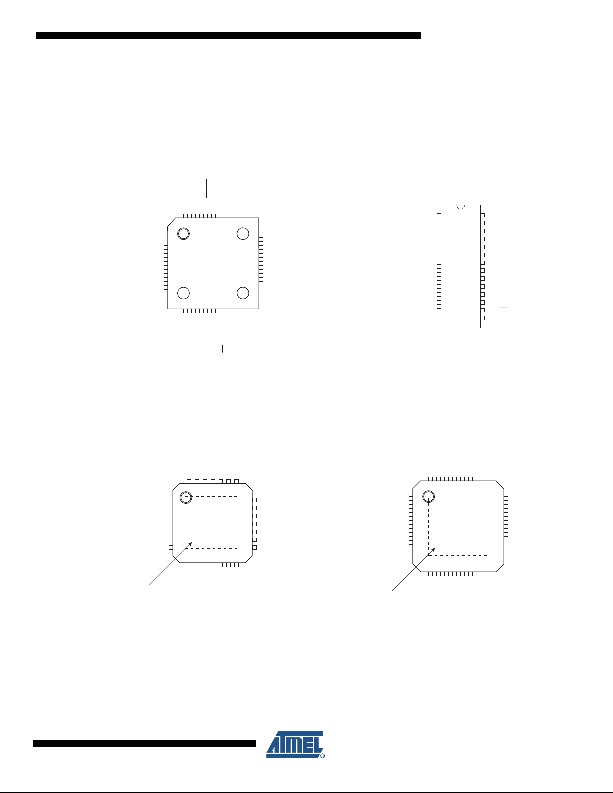
1. Pin Configurations
Figure 1-1. Pinout ATmega48/88/1682545RS
TQFP Top View
PD2 (INT0/PCINT18)
PD1 (TXD/PCINT17)
PD0 (RXD/PCINT16)
PC6 (RESET/PCINT14)
PC5 (ADC5/SCL/PCINT13)
PC4 (ADC4/SDA/PCINT12)
PC3 (ADC3/PCINT11)
32313029282726
GND
VCC
GND
VCC
1
2
3
4
5
6
7
8
9101112131415
(PCINT19/OC2B/INT1) PD3
(PCINT20/XCK/T0) PD4
(PCINT6/XTAL1/TOSC1) PB6
(PCINT7/XTAL2/TOSC2) PB7
PC2 (ADC2/PCINT10)
25
24
PC1 (ADC1/PCINT9)
23
PC0 (ADC0/PCINT8)
22
ADC7
21
GND
20
AREF
19
ADC6
18
AVC C
17
PB5 (SCK/PCINT5)
16
ATmega48/88/168
(PCINT14/RESET) PC6
(PCINT16/RXD) PD0
(PCINT17/TXD) PD1
(PCINT18/INT0) PD2
(PCINT19/OC2B/INT1) PD3
(PCINT20/XCK/T0) PD4
(PCINT6/XTAL1/TOSC1) PB6
(PCINT7/XTAL2/TOSC2) PB7
(PCINT21/OC0B/T1) PD5
(PCINT22/OC0A/AIN0) PD6
(PCINT23/AIN1) PD7
(PCINT0/CLKO/ICP1) PB0
VCC
GND
1
2
3
4
5
6
7
8
9
10
11
12
13
14
PDIP
28
PC5 (ADC5/SCL/PCINT13)
27
PC4 (ADC4/SDA/PCINT12)
26
PC3 (ADC3/PCINT11)
25
PC2 (ADC2/PCINT10)
24
PC1 (ADC1/PCINT9)
23
PC0 (ADC0/PCINT8)
22
GND
21
AREF
20
AVC C
19
PB5 (SCK/PCINT5)
18
PB4 (MISO/PCINT4)
17
PB3 (MOSI/OC2A/PCINT3)
16
PB2 (SS/OC1B/PCINT2)
15
PB1 (OC1A/PCINT1)
(PCINT19/OC2B/INT1) PD3
(PCINT20/XCK/T0) PD4
(PCINT6/XTAL1/TOSC1) PB6
(PCINT7/XTAL2/TOSC2) PB7
(PCINT21/OC0B/T1) PD5
NOTE: Bottom pad should be soldered to ground.
VCC
GND
(PCINT1/OC1A) PB1
(PCINT23/AIN1) PD7
(PCINT21/OC0B/T1) PD5
(PCINT0/CLKO/ICP1) PB0
(PCINT22/OC0A/AIN0) PD6
28 MLF Top View
PD2 (INT0/PCINT18)
PD1 (TXD/PCINT17)
PD0 (RXD/PCINT16)
PC6 (RESET/PCINT14)
PC5 (ADC5/SCL/PCINT13)
28272625242322
1
2
3
4
5
6
7
891011121314
(PCINT1/OC1A) PB1
(PCINT23/AIN1) PD7
(PCINT2/SS/OC1B) PB2
(PCINT0/CLKO/ICP1) PB0
(PCINT22/OC0A/AIN0) PD6
(PCINT4/MISO) PB4
(PCINT2/SS/OC1B) PB2
(PCINT3/OC2A/MOSI) PB3
PC4 (ADC4/SDA/PCINT12)
PC3 (ADC3/PCINT11)
PC2 (ADC2/PCINT10)
21
PC1 (ADC1/PCINT9)
20
PC0 (ADC0/PCINT8)
19
GND
18
AREF
17
AVC C
16
PB5 (SCK/PCINT5)
15
(PCINT4/MISO) PB4
(PCINT3/OC2A/MOSI) PB3
(PCINT19/OC2B/INT1) PD3
(PCINT20/XCK/T0) PD4
(PCINT6/XTAL1/TOSC1) PB6
(PCINT7/XTAL2/TOSC2) PB7
NOTE: Bottom pad should be soldered to ground.
GND
VCC
GND
VCC
1
2
3
4
5
6
7
8
32 MLF Top View
PD2 (INT0/PCINT18)
PD1 (TXD/PCINT17)
PD0 (RXD/PCINT16)
PC6 (RESET/PCINT14)
PC5 (ADC5/SCL/PCINT13)
PC4 (ADC4/SDA/PCINT12)
PC3 (ADC3/PCINT11)
32313029282726
9101112131415
(PCINT1/OC1A) PB1
(PCINT23/AIN1) PD7
(PCINT21/OC0B/T1) PD5
(PCINT22/OC0A/AIN0) PD6
(PCINT2/SS/OC1B) PB2
(PCINT0/CLKO/ICP1) PB0
(PCINT3/OC2A/MOSI) PB3
PC2 (ADC2/PCINT10)
25
PC1 (ADC1/PCINT9)
24
PC0 (ADC0/PCINT8)
23
ADC7
22
GND
21
AREF
20
ADC6
19
AVC C
18
PB5 (SCK/PCINT5)
17
16
(PCINT4/MISO) PB4
2545RS–AVR–07/09
2

1.1 Pin Descriptions
1.1.1 VCC
Digital supply voltage.
1.1.2 GND
Ground.
1.1.3 Port B (PB7:0) XTAL1/XTAL2/TOSC1/TOSC2
Port B is an 8-bit bi-directional I/O port with internal pull-up resistors (selected for each bit). The
Port B output buffers have symmetrical drive characteristics with both high sink and source
capability. As inputs, Port B pins that are externally pulled low will source current if the pull-up
resistors are activated. The Port B pins are tri-stated when a reset condition becomes active,
even if the clock is not running.
Depending on the clock selection fuse settings, PB6 can be used as input to the inverting Oscillator amplifier and input to the internal clock operating circuit.
Depending on the clock selection fuse settings, PB7 can be used as output from the inverting
Oscillator amplifier.
ATmega48/88/168
1.1.4 Port C (PC5:0)
1.1.5 PC6/RESET
If the Internal Calibrated RC Oscillator is used as chip clock source, PB7..6 is used as TOSC2..1
input for the Asynchronous Timer/Counter2 if the AS2 bit in ASSR is set.
The various special features of Port B are elaborated in “Alternate Functions of Port B” on page
77 and “System Clock and Clock Options” on page 26.
Port C is a 7-bit bi-directional I/O port with internal pull-up resistors (selected for each bit). The
PC5..0 output buffers have symmetrical drive characteristics with both high sink and source
capability. As inputs, Port C pins that are externally pulled low will source current if the pull-up
resistors are activated. The Port C pins are tri-stated when a reset condition becomes active,
even if the clock is not running.
If the RSTDISBL Fuse is programmed, PC6 is used as an I/O pin. Note that the electrical characteristics of PC6 differ from those of the other pins of Port C.
If the RSTDISBL Fuse is unprogrammed, PC6 is used as a Reset input. A low level on this pin
for longer than the minimum pulse length will generate a Reset, even if the clock is not running.
The minimum pulse length is given in Table 26-3 on page 306. Shorter pulses are not guaranteed to generate a Reset.
The various special features of Port C are elaborated in “Alternate Functions of Port C” on page
80.
1.1.6 Port D (PD7:0)
2545RS–AVR–07/09
Port D is an 8-bit bi-directional I/O port with internal pull-up resistors (selected for each bit). The
Port D output buffers have symmetrical drive characteristics with both high sink and source
capability. As inputs, Port D pins that are externally pulled low will source current if the pull-up
3

ATmega48/88/168
resistors are activated. The Port D pins are tri-stated when a reset condition becomes active,
even if the clock is not running.
The various special features of Port D are elaborated in “Alternate Functions of Port D” on page
83.
1.1.7 AV
CC
AVCC is the supply voltage pin for the A/D Converter, PC3:0, and ADC7:6. It should be externally
connected to V
, even if the ADC is not used. If the ADC is used, it should be connected to V
CC
through a low-pass filter. Note that PC6..4 use digital supply voltage, VCC.
1.1.8 AREF
AREF is the analog reference pin for the A/D Converter.
1.1.9 ADC7:6 (TQFP and QFN/MLF Package Only)
In the TQFP and QFN/MLF package, ADC7:6 serve as analog inputs to the A/D converter.
These pins are powered from the analog supply and serve as 10-bit ADC channels.
CC
2545RS–AVR–07/09
4

2. Overview
2.1 Block Diagram
ATmega48/88/168
The ATmega48/88/168 is a low-power CMOS 8-bit microcontroller based on the AVR enhanced
RISC architecture. By executing powerful instructions in a single clock cycle, the
ATmega48/88/168 achieves throughputs approaching 1 MIPS per MHz allowing the system
designer to optimize power consumption versus processing speed.
Figure 2-1. Block Diagram
Powe r
RESET
Comp.
VCC
debugWIRE
PROGRAM
CPU
Internal
Bandgap
LOGIC
SRAMFlash
AVC C
AREF
GND
2
6
GND
Watchdog
Timer
Watchdog
Oscillator
Oscillator
Circuits /
Clock
Generation
EEPROM
8bit T/C 2
DATA B US
Supervision
POR / BOD &
16bit T/C 18bit T/C 0 A/D Conv.
Analog
2545RS–AVR–07/09
USART 0
SPI TWI
PORT C (7)PORT B (8)PORT D (8)
RESET
XTAL[1..2]
ADC[6..7]PC[0..6]PB[0..7]PD[0..7]
The AVR core combines a rich instruction set with 32 general purpose working registers. All the
32 registers are directly connected to the Arithmetic Logic Unit (ALU), allowing two independent
registers to be accessed in one single instruction executed in one clock cycle. The resulting
5

ATmega48/88/168
architecture is more code efficient while achieving throughputs up to ten times faster than conventional CISC microcontrollers.
The ATmega48/88/168 provides the following features: 4K/8K/16K bytes of In-System Programmable Flash with Read-While-Write capabilities, 256/512/512 bytes EEPROM, 512/1K/1K bytes
SRAM, 23 general purpose I/O lines, 32 general purpose working registers, three flexible
Timer/Counters with compare modes, internal and external interrupts, a serial programmable
USART, a byte-oriented 2-wire Serial Interface, an SPI serial port, a 6-channel 10-bit ADC (8
channels in TQFP and QFN/MLF packages), a programmable Watchdog Timer with internal
Oscillator, and five software selectable power saving modes. The Idle mode stops the CPU
while allowing the SRAM, Timer/Counters, USART, 2-wire Serial Interface, SPI port, and interrupt system to continue functioning. The Power-down mode saves the register contents but
freezes the Oscillator, disabling all other chip functions until the next interrupt or hardware reset.
In Power-save mode, the asynchronous timer continues to run, allowing the user to maintain a
timer base while the rest of the device is sleeping. The ADC Noise Reduction mode stops the
CPU and all I/O modules except asynchronous timer and ADC, to minimize switching noise during ADC conversions. In Standby mode, the crystal/resonator Oscillator is running while the rest
of the device is sleeping. This allows very fast start-up combined with low power consumption.
The device is manufactured using Atmel’s high density non-volatile memory technology. The
On-chip ISP Flash allows the program memory to be reprogrammed In-System through an SPI
serial interface, by a conventional non-volatile memory programmer, or by an On-chip Boot program running on the AVR core. The Boot program can use any interface to download the
application program in the Application Flash memory. Software in the Boot Flash section will
continue to run while the Application Flash section is updated, providing true Read-While-Write
operation. By combining an 8-bit RISC CPU with In-System Self-Programmable Flash on a
monolithic chip, the Atmel ATmega48/88/168 is a powerful microcontroller that provides a highly
flexible and cost effective solution to many embedded control applications.
The ATmega48/88/168 AVR is supported with a full suite of program and system development
tools including: C Compilers, Macro Assemblers, Program Debugger/Simulators, In-Circuit Emulators, and Evaluation kits.
2.2 Comparison Between ATmega48, ATmega88, and ATmega168
The ATmega48, ATmega88 and ATmega168 differ only in memory sizes, boot loader support,
and interrupt vector sizes. Table 2-1 summarizes the different memory and interrupt vector sizes
for the three devices.
Table 2-1. Memory Size Summary
Device Flash EEPROM RAM Interrupt Vector Size
ATmega48 4K Bytes 256 Bytes 512 Bytes 1 instruction word/vector
ATmega88 8K Bytes 512 Bytes 1K Bytes 1 instruction word/vector
ATmega168 16K Bytes 512 Bytes 1K Bytes 2 instruction words/vector
ATmega88 and ATmega168 support a real Read-While-Write Self-Programming mechanism.
There is a separate Boot Loader Section, and the SPM instruction can only execute from there.
In ATmega48, there is no Read-While-Write support and no separate Boot Loader Section. The
SPM instruction can execute from the entire Flash.
2545RS–AVR–07/09
6

3. About
3.1 Resources
A comprehensive set of development tools, application notes and datasheets are available for
download on http://www.atmel.com/avr.
3.2 Data Retention
Reliability Qualification results show that the projected data retention failure rate is much less
than 1 PPM over 20 years at 85°C or 100 years at 25°C.
3.3 Code Examples
This documentation contains simple code examples that briefly show how to use various parts of
the device. These code examples assume that the part specific header file is included before
compilation. Be aware that not all C compiler vendors include bit definitions in the header files
and interrupt handling in C is compiler dependent. Please confirm with the C compiler documentation for more details.
For I/O Registers located in extended I/O map, “IN”, “OUT”, “SBIS”, “SBIC”, “CBI”, and “SBI”
instructions must be replaced with instructions that allow access to extended I/O. Typically
“LDS” and “STS” combined with “SBRS”, “SBRC”, “SBR”, and “CBR”.
ATmega48/88/168
2545RS–AVR–07/09
7
ATmega48/88/168
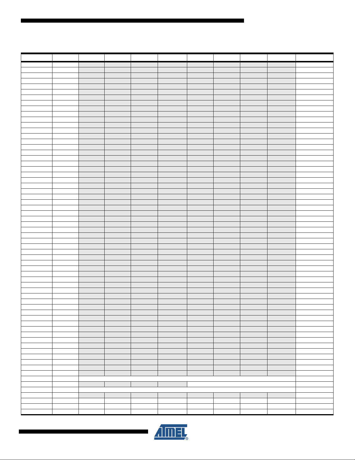
4. Register Summary
Address Name Bit 7 Bit 6 Bit 5 Bit 4 Bit 3 Bit 2 Bit 1 Bit 0 Page
(0xFF) Reserved – – – – – – – –
(0xFE) Reserved – – – – – – – –
(0xFD) Reserved – – – – – – – –
(0xFC) Reserved
(0xFB) Reserved
(0xFA) Reserved – – – – – – – –
(0xF9) Reserved – – – – – – – –
(0xF8) Reserved – – – – – – – –
(0xF7) Reserved – – – – – – – –
(0xF6) Reserved – – – – – – – –
(0xF5) Reserved – – – – – – – –
(0xF4) Reserved – – – – – – – –
(0xF3) Reserved – – – – – – – –
(0xF2) Reserved – – – – – – – –
(0xF1) Reserved – – – – – – – –
(0xF0) Reserved
(0xEF) Reserved
(0xEE) Reserved – – – – – – – –
(0xED) Reserved – – – – – – – –
(0xEC) Reserved – – – – – – – –
(0xEB) Reserved – – – – – – – –
(0xEA) Reserved – – – – – – – –
(0xE9) Reserved – – – – – – – –
(0xE8) Reserved – – – – – – – –
(0xE7) Reserved – – – – – – – –
(0xE6) Reserved – – – – – – – –
(0xE5) Reserved – – – – – – – –
(0xE4) Reserved – – – – – – – –
(0xE3) Reserved – – – – – – – –
(0xE2) Reserved – – – – – – – –
(0xE1) Reserved – – – – – – – –
(0xE0) Reserved – – – – – – – –
(0xDF) Reserved – – – – – – – –
(0xDE) Reserved – – – – – – – –
(0xDD) Reserved – – – – – – – –
(0xDC) Reserved – – – – – – – –
(0xDB) Reserved – – – – – – – –
(0xDA) Reserved – – – – – – – –
(0xD9) Reserved – – – – – – – –
(0xD8) Reserved – – – – – – – –
(0xD7) Reserved – – – – – – – –
(0xD6) Reserved – – – – – – – –
(0xD5) Reserved
(0xD4) Reserved
(0xD3) Reserved – – – – – – – –
(0xD2) Reserved
(0xD1) Reserved
(0xD0) Reserved
(0xCF) Reserved – – – – – – – –
(0xCE) Reserved
(0xCD) Reserved
(0xCC) Reserved – – – – – – – –
(0xCB) Reserved
(0xCA) Reserved
(0xC9) Reserved – – – – – – – –
(0xC8) Reserved
(0xC7) Reserved
(0xC6) UDR0 USART I/O Data Register 189
(0xC5) UBRR0H
(0xC4) UBRR0L USART Baud Rate Register Low 193
(0xC3) Reserved
(0xC2) UCSR0C UMSEL01 UMSEL00 UPM01 UPM00 USBS0
(0xC1) UCSR0B RXCIE0 TXCIE0 UDRIE0 RXEN0 TXEN0 UCSZ02 RXB80 TXB80 190
(0xC0) UCSR0A RXC0 TXC0 UDRE0 FE0 DOR0 UPE0 U2X0 MPCM0 189
– – – – – – – –
– – – – – – – –
– – – – – – – –
– – – – – – – –
– – – – – – – –
– – – – – – – –
– – – – – – – –
– – – – – – – –
– – – – – – – –
– – – – – – – –
– – – – – – – –
– – – – – – – –
– – – – – – – –
– – – – – – – –
– – – – – – – –
USART Baud Rate Register High 193
– – – – – – – –
UCSZ01 /UDORD0 UCSZ00 / UCPHA0
UCPOL0 191/206
2545RS–AVR–07/09
8

ATmega48/88/168
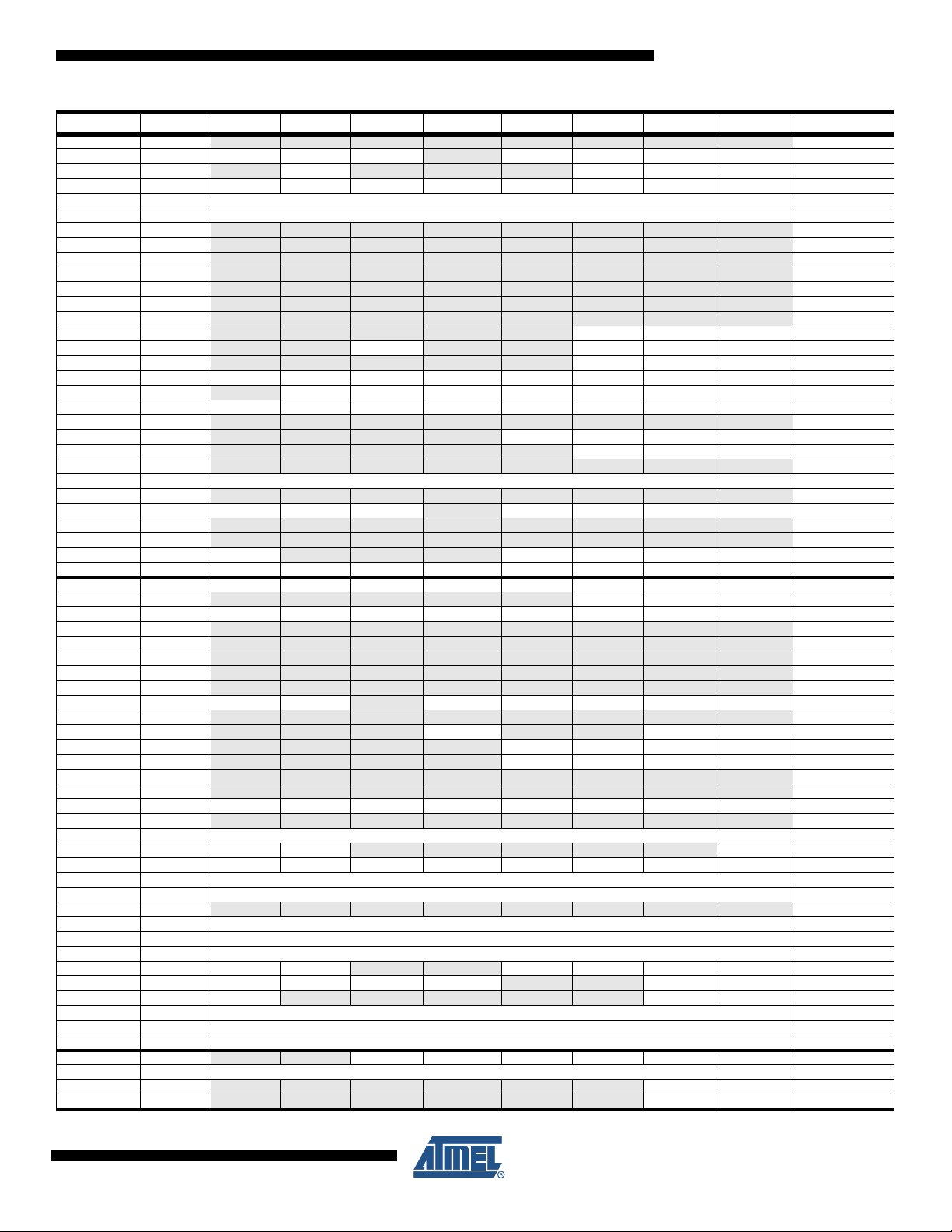
Address Name Bit 7 Bit 6 Bit 5 Bit 4 Bit 3 Bit 2 Bit 1 Bit 0 Page
(0xBF) Reserved – – – – – – – –
(0xBE) Reserved – – – – – – – –
(0xBD) TWAMR TWAM6 TWAM5 TWAM4 TWAM3 TWAM2 TWAM1 TWAM0 –238
(0xBC) TWCR TWINT TWEA TWSTA TWSTO TWWC TWEN –TWIE 235
(0xBB) TWDR 2-wire Serial Interface Data Register 237
(0xBA) TWAR TWA6 TWA5 TWA4 TWA3 TWA2 TWA1 TWA0 TWGCE 238
(0xB9) TWSR TWS7 TWS6 TWS5 TWS4 TWS3 –TWPS1TWPS0 237
(0xB8) TWBR 2-wire Serial Interface Bit Rate Register 235
(0xB7) Reserved – – – – – – –
(0xB6) ASSR – EXCLK AS2 TCN2UB OCR2AUB OCR2BUB TCR2AUB TCR2BUB 158
(0xB5) Reserved – – – – – – – –
(0xB4) OCR2B Timer/Counter2 Output Compare Register B 157
(0xB3) OCR2A Timer/Counter2 Output Compare Register A 156
(0xB2) TCNT2 Timer/Counter2 (8-bit) 156
(0xB1) TCCR2B FOC2A FOC2B – – WGM22 CS22 CS21 CS20
(0xB0) TCCR2A COM2A1 COM2A0 COM2B1 COM2B0 – –WGM21WGM20 152
(0xAF) Reserved
(0xAE) Reserved
(0xAD) Reserved – – – – – – – –
(0xAC) Reserved
(0xAB) Reserved
(0xAA) Reserved – – – – – – – –
(0xA9) Reserved – – – – – – – –
(0xA8) Reserved – – – – – – – –
(0xA7) Reserved – – – – – – – –
(0xA6) Reserved – – – – – – – –
(0xA5) Reserved – – – – – – – –
(0xA4) Reserved – – – – – – – –
(0xA3) Reserved – – – – – – – –
(0xA2) Reserved – – – – – – – –
(0xA1) Reserved – – – – – – – –
(0xA0) Reserved – – – – – – – –
(0x9F) Reserved – – – – – – – –
(0x9E) Reserved – – – – – – – –
(0x9D) Reserved – – – – – – – –
(0x9C) Reserved – – – – – – – –
(0x9B) Reserved – – – – – – – –
(0x9A) Reserved – – – – – – – –
(0x99) Reserved – – – – – – – –
(0x98) Reserved – – – – – – – –
(0x97) Reserved – – – – – – – –
(0x96) Reserved – – – – – – – –
(0x95) Reserved – – – – – – – –
(0x94) Reserved
(0x93) Reserved
(0x92) Reserved – – – – – – – –
(0x91) Reserved
(0x90) Reserved
(0x8F) Reserved
(0x8E) Reserved – – – – – – – –
(0x8D) Reserved
(0x8C) Reserved
(0x8B) OCR1BH Timer/Counter1 - Output Compare Register B High Byte 133
(0x8A) OCR1BL Timer/Counter1 - Output Compare Register B Low Byte 133
(0x89) OCR1AH Timer/Counter1 - Output Compare Register A High Byte 133
(0x88) OCR1AL Timer/Counter1 - Output Compare Register A Low Byte 133
(0x87) ICR1H Timer/Counter1 - Input Capture Register High Byte 134
(0x86) ICR1L Timer/Counter1 - Input Capture Register Low Byte 134
(0x85) TCNT1H Timer/Counter1 - Counter Register High Byte 133
(0x84) TCNT1L Timer/Counter1 - Counter Register Low Byte 133
(0x83) Reserved
(0x82) TCCR1C FOC1A FOC1B
(0x81) TCCR1B ICNC1 ICES1
(0x80) TCCR1A COM1A1 COM1A0 COM1B1 COM1B0 – –WGM11WGM10 129
(0x7F) DIDR1
(0x7E) DIDR0
– – – – – – – –
– – – – – – – –
– – – – – – – –
– – – – – – – –
– – – – – – – –
– – – – – – – –
– – – – – – – –
– – – – – – – –
– – – – – – – –
– – – – – – – –
– – – – – – – –
– – – – – – – –
– – – – – –132
– WGM13 WGM12 CS12 CS11 CS10 131
– – – – – –AIN1DAIN0D 242
– – ADC5D ADC4D ADC3D ADC2D ADC1D ADC0D 258
155
2545RS–AVR–07/09
9
ATmega48/88/168
Address Name Bit 7 Bit 6 Bit 5 Bit 4 Bit 3 Bit 2 Bit 1 Bit 0 Page
(0x7D) Reserved – – – – – – – –
(0x7C) ADMUX REFS1 REFS0 ADLAR – MUX3 MUX2 MUX1 MUX0 254
(0x7B) ADCSRB –ACME – – – ADTS2 ADTS1 ADTS0 257
(0x7A) ADCSRA ADEN ADSC ADATE ADIF ADIE ADPS2 ADPS1 ADPS0 255
(0x79) ADCH ADC Data Register High byte 257
(0x78) ADCL ADC Data Register Low byte 257
(0x77) Reserved – – – – – – – –
(0x76) Reserved – – – – – – – –
(0x75) Reserved – – – – – – – –
(0x74) Reserved – – – – – – – –
(0x73) Reserved – – – – – – – –
(0x72) Reserved – – – – – – – –
(0x71) Reserved – – – – – – – –
(0x70) TIMSK2 – – – – – OCIE2B OCIE2A TOIE2 157
(0x6F) TIMSK1 – –ICIE1 – – OCIE1B OCIE1A TOIE1 134
(0x6E) TIMSK0 – – – – – OCIE0B OCIE0A TOIE0 105
(0x6D) PCMSK2 PCINT23 PCINT22 PCINT21 PCINT20 PCINT19 PCINT18 PCINT17 PCINT16 69
(0x6C) PCMSK1 – PCINT14 PCINT13 PCINT12 PCINT11 PCINT10 PCINT9 PCINT8 69
(0x6B) PCMSK0 PCINT7 PCINT6 PCINT5 PCINT4 PCINT3 PCINT2 PCINT1 PCINT0 69
(0x6A) Reserved
(0x69) EICRA
(0x68) PCICR – – – – – PCIE2 PCIE1 PCIE0
(0x67) Reserved – – – – – – – –
(0x66) OSCCAL Oscillator Calibration Register 36
(0x65) Reserved – – – – – – – –
(0x64) PRR PRTWI PRTIM2 PRTIM0 – PRTIM1 PRSPI PRUSART0 PRADC 40
(0x63) Reserved – – – – – – – –
(0x62) Reserved – – – – – – – –
(0x61) CLKPR CLKPCE – – – CLKPS3 CLKPS2 CLKPS1 CLKPS0 36
(0x60) WDTCSR WDIF WDIE WDP3 WDCE WDE WDP2 WDP1 WDP0 52
0x3F (0x5F) SREG I T H S V N Z C 10
0x3E (0x5E) SPH – – – – – (SP10)
0x3D (0x5D) SPL SP7 SP6 SP5 SP4 SP3 SP2 SP1 SP0 12
0x3C (0x5C) Reserved – – – – – – – –
0x3B (0x5B) Reserved – – – – – – – –
0x3A (0x5A) Reserved – – – – – – – –
0x39 (0x59) Reserved – – – – – – – –
0x38 (0x58) Reserved – – – – – – – –
0x37 (0x57) SPMCSR SPMIE (RWWSB)
0x36 (0x56) Reserved – – – – – – – –
0x35 (0x55) MCUCR – – –PUD– – IVSEL IVCE
0x34 (0x54) MCUSR – – – – WDRF BORF EXTRF PORF
0x33 (0x53) SMCR – – – –SM2SM1SM0SE 38
0x32 (0x52) Reserved
0x31 (0x51) Reserved
0x30 (0x50) ACSR ACD ACBG ACO ACI ACIE ACIC ACIS1 ACIS0 241
0x2F (0x4F) Reserved
0x2E (0x4E) SPDR SPI Data Register 169
0x2D (0x4D) SPSR SPIF WCOL – – – – – SPI2X 168
0x2C (0x4C) SPCR SPIE SPE DORD MSTR CPOL CPHA SPR1 SPR0 167
0x2B (0x4B) GPIOR2 General Purpose I/O Register 2 25
0x2A (0x4A) GPIOR1 General Purpose I/O Register 1 25
0x29 (0x49) Reserved – – – – – – – –
0x28 (0x48) OCR0B Timer/Counter0 Output Compare Register B
0x27 (0x47) OCR0A Timer/Counter0 Output Compare Register A
0x26 (0x46) TCNT0 Timer/Counter0 (8-bit)
0x25 (0x45) TCCR0B FOC0A FOC0B
0x24 (0x44) TCCR0A COM0A1 COM0A0 COM0B1 COM0B0
0x23 (0x43) GTCCR TSM – – – – – PSRASY PSRSYNC 138/159
0x22 (0x42) EEARH (EEPROM Address Register High Byte)
0x21 (0x41) EEARL EEPROM Address Register Low Byte 21
0x20 (0x40) EEDR EEPROM Data Register 21
0x1F (0x3F) EECR – – EEPM1 EEPM0 EERIE EEMPE EEPE EERE 21
0x1E (0x3E) GPIOR0 General Purpose I/O Register 0 25
0x1D (0x3D) EIMSK
0x1C (0x3C) EIFR
– – – – – – – –
– – – –ISC11ISC10ISC01ISC00 66
5.
5.
– – – – – – – –
– – – – – – – –
– – – – – – – –
– – – – – –INT1INT0 67
– – – – – – INTF1 INTF0 67
– (RWWSRE)
– – WGM02 CS02 CS01 CS00
5.
BLBSET PGWRT PGERS SELFPRGEN 282
– –WGM01WGM00
5.
SP9 SP8 12
21
2545RS–AVR–07/09
10
ATmega48/88/168
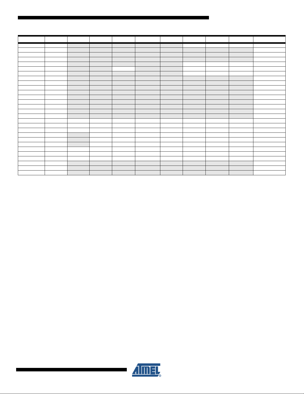
Address Name Bit 7 Bit 6 Bit 5 Bit 4 Bit 3 Bit 2 Bit 1 Bit 0 Page
0x1B (0x3B) PCIFR – – – – – PCIF2 PCIF1 PCIF0
0x1A (0x3A) Reserved – – – – – – – –
0x19 (0x39) Reserved – – – – – – – –
0x18 (0x38) Reserved – – – – – – – –
0x17 (0x37) TIFR2 – – – – – OCF2B OCF2A TOV2 157
0x16 (0x36) TIFR1 – –ICF1 – – OCF1B OCF1A TOV1 135
0x15 (0x35) TIFR0 – – – – – OCF0B OCF0A TOV0
0x14 (0x34) Reserved – – – – – – – –
0x13 (0x33) Reserved – – – – – – – –
0x12 (0x32) Reserved – – – – – – – –
0x11 (0x31) Reserved – – – – – – – –
0x10 (0x30) Reserved – – – – – – – –
0x0F (0x2F) Reserved – – – – – – – –
0x0E (0x2E) Reserved – – – – – – – –
0x0D (0x2D) Reserved – – – – – – – –
0x0C (0x2C) Reserved – – – – – – – –
0x0B (0x2B) PORTD PORTD7 PORTD6 PORTD5 PORTD4 PORTD3 PORTD2 PORTD1 PORTD0 87
0x0A (0x2A) DDRD DDD7 DDD6 DDD5 DDD4 DDD3 DDD2 DDD1 DDD0 87
0x09 (0x29) PIND PIND7 PIND6 PIND5 PIND4 PIND3 PIND2 PIND1 PIND0 87
0x08 (0x28) PORTC
0x07 (0x27) DDRC
0x06 (0x26) PINC – PINC6 PINC5 PINC4 PINC3 PINC2 PINC1 PINC0 86
0x05 (0x25) PORTB PORTB7 PORTB6 PORTB5 PORTB4 PORTB3 PORTB2 PORTB1 PORTB0 86
0x04 (0x24) DDRB DDB7 DDB6 DDB5 DDB4 DDB3 DDB2 DDB1 DDB0 86
0x03 (0x23) PINB PINB7 PINB6 PINB5 PINB4 PINB3 PINB2 PINB1 PINB0 86
0x02 (0x22) Reserved – – – – – – – –
0x01 (0x21) Reserved – – – – – – – –
0x0 (0x20) Reserved – – – – – – – –
Note: 1. For compatibility with future devices, reserved bits should be written to zero if accessed. Reserved I/O memory addresses
should never be written.
2. I/O Registers within the address range 0x00 - 0x1F are directly bit-accessible using the SBI and CBI instructions. In these
registers, the value of single bits can be checked by using the SBIS and SBIC instructions.
3. Some of the Status Flags are cleared by writing a logical one to them. Note that, unlike most other AVRs, the CBI and SBI
instructions will only operate on the specified bit, and can therefore be used on registers containing such Status Flags. The
CBI and SBI instructions work with registers 0x00 to 0x1F only.
4. When using the I/O specific commands IN and OUT, the I/O addresses 0x00 - 0x3F must be used. When addressing I/O
Registers as data space using LD and ST instructions, 0x20 must be added to these addresses. The ATmega48/88/168 is a
complex microcontroller with more peripheral units than can be supported within the 64 location reserved in Opcode for the
IN and OUT instructions. For the Extended I/O space from 0x60 - 0xFF in SRAM, only the ST/STS/STD and LD/LDS/LDD
instructions can be used.
5. Only valid for ATmega88/168
– PORTC6 PORTC5 PORTC4 PORTC3 PORTC2 PORTC1 PORTC0 86
– DDC6 DDC5 DDC4 DDC3 DDC2 DDC1 DDC0 86
2545RS–AVR–07/09
11
 Loading...