

Page 1

BDTIC www.bdtic.com/ATMEL
Features
• High Performance, Low Power AVR ® 8-bit Microcontroller
• Advanced RISC Architecture
– 131 Powerful Instructions - Most Single Clock Cycle Execution
– 32 x 8 General Purpose Working Registers
– Fully Static Ope ration
– Up to 1 MIPS throughput per MHz
– On-chip 2-cycle Multiplier
• Data and Non-Volatile Program Memory
– 16K/32K/64K Bytes Flash of In-System Programmab le Program Memory
• Endurance: 10,000 Write/Erase Cycles
– Optional Boot Code Section with Independent Lock Bits
– In-System Programming by On-chip Boot Program
• True Read-While-Write Operation
– 512/1024/2048 Bytes of In-System Programmable EEPROM
• Endurance: 50,000 Write/Erase Cycles
• Programming Lock for Flash Program and EEPROM Data Security
• 1024/2048/4096 Bytes Internal SRAM
• On Chip Debug Interface (debugWIRE)
• CAN 2.0A/B with 6 Message Objects - ISO 16845 Certified
• LIN 2.1 and 1.3 Controller or 8-Bit UART
• One 12-bit High Speed PSC (Power Stage Controller) (only ATmega16/32/64M1)
• Non Overlapping Inverted PWM Output Pins With Flexible Dead-Time
• Variable PWM duty Cycle and Frequency
• Synchronous Update of all PWM Registers
• Auto Stop Function for Emergency Event
• Peripheral Features
– One 8-bit General purpose T imer/Co unte r with Separate Prescaler, Compa re Mode
and Capture Mode
– One 16-bit General purpose Timer/Counter with Separate Prescaler, Compare
Mode and Capture Mode
– One Master/Slave SPI Serial Interface
– 10-bit ADC
• Up To 11 Single Ended Channels and 3 Fully Differential ADC Channel Pairs
• Programmable Gain (5x, 10x, 20x, 40x) on Differential Channels
• Internal Reference Voltage
• Direct Power Supply Voltage Measurement
– 10-bit DAC for Variable Voltage Reference (Comparators, ADC)
– Four Analog Comparators with Variable Threshold Detection
– 100µA ±3% Current Source (LIN Node Identification)
– Interrupt and Wake-up on Pin Change
– Programmable Watchdog Timer with Separate On-Chip Oscillator
– On-chipTemperature Sensor
• Special Microcontroller Features
– Low Power Idle, Noise Reduction, and Power Down Modes
– Power On Reset and Programmable Brown Out Detection
– In-System Programmable via SPI Port
– High Precision Crystal Oscillator for CAN Operations (16 MHz)
(1)
8-bit
Microcontroller
with
16K/32K/64K
Bytes In-System
Programmable
Flash
ATmega16M1
ATmega32M1
ATmega64M1
ATmega32C1
ATmega64C1
Automotive
Preliminary
1. See certification on Atmel web site. And note on Section 16.4.3 on page 176.
7647D–AVR–08/08
Page 2

Page 3
ATmega16/32/64/M1/C1
– Internal Calibrated RC Oscillator ( 8 MHz)
– On-chip PLL for fast PWM ( 32 MHz, 64 MHz) and CPU (16 MHz)
• Operating Voltage: 2.7V - 5.5V
• Extended Operating Temperature:
– -40°C to +125°C
• Core Speed Grade:
– 0 - 8MHz @ 2.7 - 4.5V
– 0 - 16MHz @ 4.5 - 5.5V
ATmega32/64/M1/C1 Produ ct Line- up
Part number ATmega32C1 ATmega64C1 ATmega16M1 ATmega32M1 ATmega64M1
Flash Size 32 Kbyte 64 Kbyte 16 Kbyte 32 Kbyte 64 Kbyte
RAM Size 2048 bytes 4096 bytes 1024 bytes 2048 bytes 4096 bytes
EEPROM Size 1024 bytes 2048 bytes 512 bytes 1024 bytes 2048 bytes
8-bit Timer Yes
16-bit Timer Yes
PSC No Yes
PWM Outputs4 4 101010
Fault Inputs (PSC) 00333
PLL 32/64 MHz
10-bit ADC Channels
10-bit DAC Yes
Analog Comparators 4
Current Source Yes
CAN Yes
LIN/UART Yes
On-Chip Temp. Sensor Y es
SPI Interface Yes
11 single
3 Differential
7647D–AVR–08/08
3
Page 4

ATmega16/32/64/M1/C1
1. Pin Configurations
Figure 1-1. ATmega16/32/64M1 TQFP32/QFN32 (7*7 mm) Package.
ATmega32/64M1 TQFP32/QFN32
(PCINT17/PSCIN0/CLKO)
PD1
(PCINT24/RESET/OCD)
PE0
(PCINT16/PSCOUT0A)
(PCINT8/INT3/PSCOUT1A)
PC0
PD0
PB7 (ADC4/PSCOUT0B/SCK/PCINT7)
PB6 (ADC7/PSCOUT1B/PCINT6)
PB5 (ADC6/INT2/ACMPN1/AMP2-/PCINT5)
PC7 (D2A/AMP2+/PCINT15)
(PCINT18/PSCIN2/OC1A/MISO_A) PD2
(PCINT19/TXD/TXLIN/OC0A/SS/MOSI_A) PD3
(PCINT9/PSCIN1/OC1B/SS_A) PC1
VCC
GND
(PCINT10/T0/TXCAN) PC2
(PCINT11/T1/RXCAN/ICP1B) PC3
(PCINT0/MISO/PSCOUT2A) PB0
32313029282726
1
2
3
4
5
6
7
8
9101112131415
(PCINT25/OC0B/XTAL1) PE1
(PCINT1/MOSI/PSCOUT2B) PB1
(PCINT26/ADC0/XTAL2) PE2
(ADC2/ACMP2/PCINT21) PD5
(ADC3/ACMPN2/INT0/PCINT22) PD6
(PCINT20/ADC1/RXD/RXLIN/ICP1A/SCK_A) PD4
25
24
PB4 (AMP0+/PCINT4)
23
PB3 (AMP0-/PCINT3)
22
PC6 (ADC10/ACMP1/PCINT14)
AREF(ISRC)
21
AGND
20
AVCC
19
PC5 (ADC9/ACMP3/AMP1+/PCINT13)
18
PC4 (ADC8/ACMPN3/AMP1-/PCINT12)
17
16
(ACMP0/PCINT23) PD7
(ADC5/INT1/ACMPN0/PCINT2) PB2
Note: On the engineering samp les (Parts marked AT90PWM32 4), the ACM PN3 altern ate func tion i s not
located on PC4. It is located on PE2.
4
7647D–AVR–08/08
Page 5

ATmega16/32/64/M1/C1
Figure 1-2. ATmega32/64C1 TQFP32/QFN32 (7*7 mm) Package
ATmega32/64C1 TQFP32/QFN32
(PCINT16)
(PCINT24/RESET/OCD)
(PCINT17/CLKO)
(PCINT8/INT3)
PD1
PE0
PC0
PD0
PB7 (ADC4/SCK/PCINT7)
PB6 (ADC7PCINT6)
PB5 (ADC6/INT2/ACMPN1/AMP2-/PCINT5)
PC7 (D2A/AMP2+/PCINT15)
(PCINT18/OC1A/MISO_A) PD2
(PCINT19/TXD/TXLIN/OC0A/SS/MOSI_A) PD3
(PCINT9/OC1B/SS_A) PC1
VCC
GND
(PCINT10/T0/TXCAN) PC2
(PCINT11/T1/RXCAN/ICP1B) PC3
(PCINT0/MISO) PB0
32313029282726
1
2
3
4
5
6
7
8
9101112131415
(PCINT1/MOSI) PB1
(PCINT25/OC0B/XTAL1) PE1
25
24
PB4 (AMP0+/PCINT4)
23
PB3 (AMP0-/PCINT3)
22
PC6 (ADC10/ACMP1/PCINT14)
AREF(ISRC)
21
AGND
20
AVCC
19
PC5 (ADC9/ACMP3/AMP1+/PCINT13)
18
PC4 (ADC8/ACMPN3/AMP1-/PCINT12)
17
16
(ACMP0/PCINT23) PD7
(PCINT26/ADC0/XTAL2) PE2
(ADC2/ACMP2/PCINT21) PD5
(ADC5/INT1/ACMPN0/PCINT2) PB2
(ADC3/ACMPN2/INT0/PCINT22) PD6
(PCINT20/ADC1/RXD/RXLIN/ICP1A/SCK_A) PD4
7647D–AVR–08/08
Note: On the first engi neering s amples (Part s mark ed AT90PWM3 24), the ACMPN 3 altern ate function is
not located on PC4. It is located on PE2.
5
Page 6

ATmega16/32/64/M1/C1
1.1 Pin Descriptions
:
Table 1-1. Pin out description
QFN32 Pin
Number Mnemonic Type Name, Function & Alternate Function
5GNDPowerGround: 0V reference
20 AGND Power Analog Ground: 0V reference for analog part
4 VCC Power Power Supply
Analog Power Supply: This is the power supply voltage for analog
19 AVCC Power
21 AREF Power
part
For a normal use this pin must be connected.
Analog Reference : reference for analog converter . This is the
reference voltage of the A/D converter. As output, can be used by
external analog
ISRC (Current Source Output)
MISO (SPI Master In Slave Out)
8PB0I/O
9PB1I/O
16 PB2 I/O
23 PB3 I/O
24 PB4 I/O
26 PB5 I/O
27 PB6 I/O
PSCOUT2A
PCINT0 (Pin Change Interrupt 0)
MOSI (SPI Master Out Slave In)
PSCOUT2B
PCINT1 (Pin Change Interrupt 1)
ADC5 (Analog Input Channel 5 )
INT1 (External Interrupt 1 Input)
ACMPN0 (Analog Comparator 0 Negative Input)
PCINT2 (Pin Change Interrupt 2)
AMP0- (Analog Differential Amplifier 0 Negative Input)
PCINT3 (Pin Change Interrupt 3)
AMP0+ (Analog Differential Amplifier 0 Positive Input)
PCINT4 (Pin Change Interrupt 4)
ADC6 (Analog Input Channel 6)
INT2 (External Interrupt 2 Input)
ACMPN1 (Analog Comparator 1 Negative Input)
AMP2- (Analog Differential Amplifier 2 Negative Input)
PCINT5 (Pin Change Interrupt 5)
ADC7 (Analog Input Channel 7)
PSCOUT1B
PCINT6 (Pin Change Interrupt 6)
(1)
(PSC Module 2 Output A)
(1)
(PSC Module 2 Output B)
(1)
(PSC Module 1 Output A)
28 PB7 I/O
30 PC0 I/O
6
ADC4 (Analog Input Channel 4)
PSCOUT0B
SCK (SPI Clock)
PCINT7 (Pin Change Interrupt 7)
PSCOUT1A
INT3 (External Interrupt 3 Input)
PCINT8 (Pin Change Interrupt 8)
(1)
(PSC Module 0 Output B)
(1)
(PSC Module 1 Output A)
7647D–AVR–08/08
Page 7

ATmega16/32/64/M1/C1
Table 1-1. Pin out description (Continued)
QFN32 Pin
Number Mnemonic Type Name, Function & Alternate Function
PSCIN1 (PSC Digital Input 1)
3PC1I/O
6PC2I/O
7PC3I/O
17 PC4
I/O
OC1B (Timer 1 Output Compare B)
SS_A (Alternate SPI Slave Select)
PCINT9 (Pin Change Interrupt 9)
T0 (Timer 0 clock input)
TXCAN (CAN Transmit Output)
PCINT10 (Pin Change Interrupt 10)
T1 (Timer 1 clock input)
RXCAN (CAN Receive Input)
ICP1B (Timer 1 input capture alternate B input)
PCINT11 (Pin Change Interrupt 11)
ADC8 (Analog Input Channel 8)
AMP1- (Analog Differential Amplifier 1 Negative Input)
ACMPN3 (Analog Comparator 3 Negative Input )
PCINT12 (Pin Change Interrupt 12)
ADC9 (Analog Input Channel 9)
18 PC5 I/O
22 PC6 I/O
25 PC7 I/O
29 PD0 I/O
32 PD1 I/O
1PD2I/O
2PD3I/O
AMP1+ (Analog Differential Amplifier 1 Positive Input)
ACMP3 (Analog Comparator 3 Positive Input)
PCINT13 (Pin Change Interrupt 13)
ADC10 (Analog Input Channel 10)
ACMP1 (Analog Comparator 1 Positive Input )
PCINT14 (Pin Change Interrupt 14)
D2A (DAC output )
AMP2+ (Analog Differential Amplifier 2 Positive Input)
PCINT15 (Pin Change Interrupt 15)
PSCOUT0A
PCINT16 (Pin Change Interrupt 16)
PSCIN0 (PSC Digital Input 0)
CLKO (System Clock Output)
PCINT17 (Pin Change Interrupt 17)
OC1A (Timer 1 Output Compare A)
PSCIN2 (PSC Digital Input 2)
MISO_A (Programming & alternate SPI Master In Slave Out)
PCINT18 (Pin Change Interrupt 18)
TXD (UART Tx data)
TXLIN (LIN Transmit Output)
OC0A (Timer 0 Output Compare A)
SS (SPI Slave Select)
MOSI_A (Programming & alternate Master Out SPI Slave In)
PCINT19 (Pin Change Interrupt 19)
(1)
(PSC Module 0 Output A)
7647D–AVR–08/08
7
Page 8

ATmega16/32/64/M1/C1
Table 1-1. Pin out description (Continued)
QFN32 Pin
Number Mnemonic Type Name, Function & Alternate Function
ADC1 (Analog Input Channel 1)
RXD (UART Rx data)
12 PD4 I/O
13 PD5 I/O
14 PD6 I/O
RXLIN (LIN Receive Input)
ICP1A (Timer 1 input capture alternate A input)
SCK_A (Programming & alternate SPI Clock)
PCINT20 (Pin Change Interrupt 20)
ADC2 (Analog Input Channel 2)
ACMP2 (Analog Comparator 2 Positive Input )
PCINT21 (Pin Change Interrupt 21)
ADC3 (Analog Input Channel 3 )
ACMPN2 (Analog Comparator 2 Negative Input)
INT0 (External Interrupt 0 Input)
PCINT22 (Pin Change Interrupt 22)
2. Overview
15 PD7 I/O
31 PE0 I/O or I
10 PE1 I/O
11 PE2 I/O
ACMP0 (Analog Comparator 0 Positive Input )
PCINT23 (Pin Change Interrupt 23)
RESET (Reset Input)
OCD (On Chip Debug I/O)
PCINT24 (Pin Change Interrupt 24)
XTAL1 (XTAL Input)
OC0B (Timer 0 Output Compare B)
PCINT25 (Pin Change Interrupt 25)
XTAL2 (XTAL Output)
ADC0 (Analog Input Channel 0)
PCINT26 (Pin Change Interrupt 26)
Note: 1. Only for ATmega32/64M1.
2. On the first engineering samples (Parts marked AT90PWM324), the ACMPN3 alternate function is not located on PC4. It is located on PE2.
The ATmega16/32/64/M1/C1 is a low-power CMOS 8-bit microcontroller based on the AVR
enhanced RISC architecture. By executing powerful ins tructions in a singl e clock cycle , the
ATmega16/32/64/M1/C1 achieves throughputs approaching 1 MIPS per MHz allowing the system designer to optimize power consumption versus processing speed.
8
7647D–AVR–08/08
Page 9
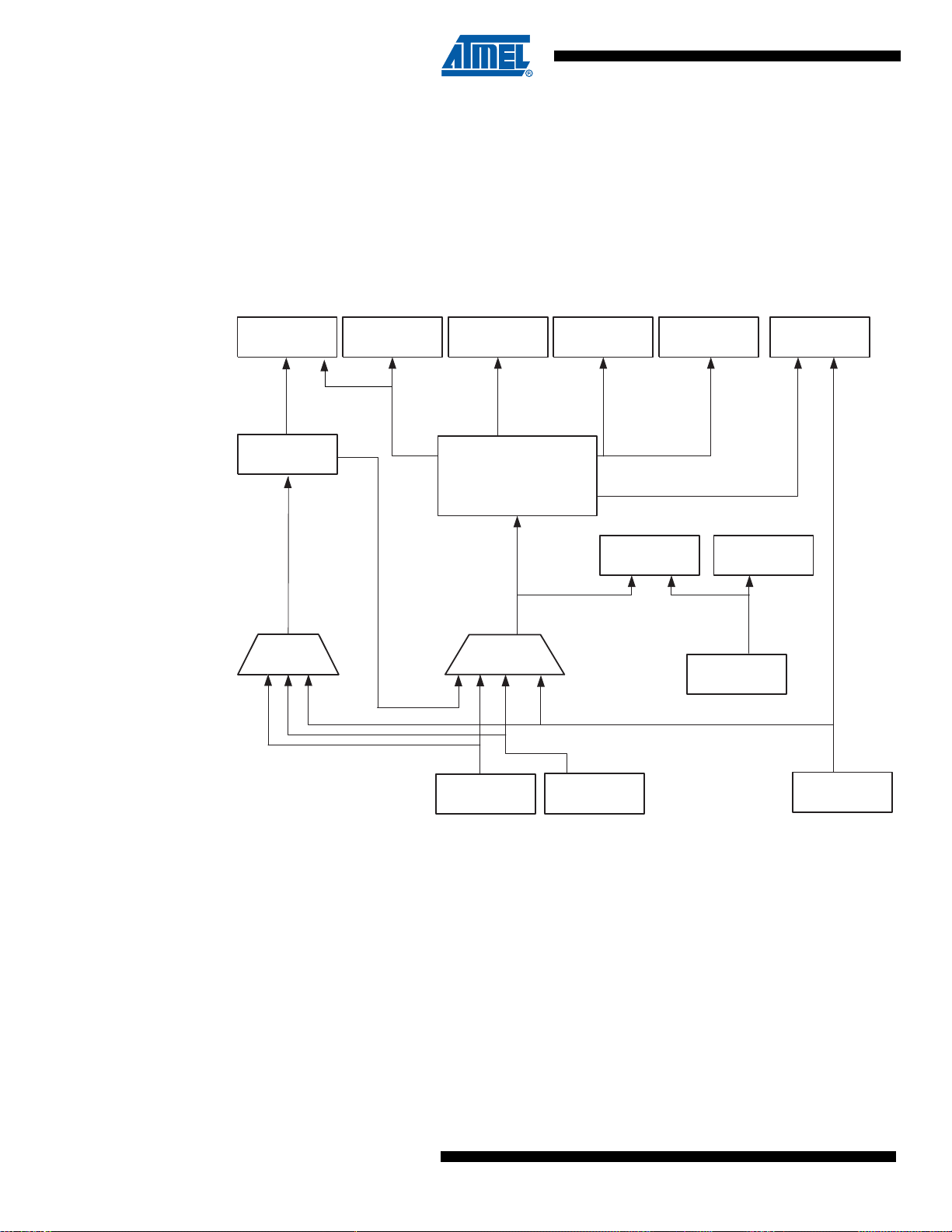
2.1 Block Diagram
Data Bus 8-bit
ATmega16/32/64/M1/C1
Figure 2-1. Block Diagram
Flash Program
Memory
Instruction
Register
Instruction
Decoder
Control Lines
Program
Counter
Direct Addressing
Status
and Control
32 x 8
General
Purpose
Registrers
ALU
Indirect Addressing
Data
SRAM
EEPROM
Interrupt
Unit
SPI
Unit
Watchdog
Timer
4 Analog
Comparators
HW LIN/UART
Timer 0
Timer 1
ADC
DAC
7647D–AVR–08/08
I/O Lines
Current Source
MPSC
CAN
The AVR core com bin es a rich in struction set with 32 g ene ra l p ur pos e worki ng re gisters. All the
32 registers are dire ctly c onn ec ted to the Ar ithmetic Logic Unit (ALU), al lo win g two ind ependent
registers to be accessed in one single instruction executed in one clock cycle. The resulting
architecture is more code efficient while achieving throughputs up to ten times faster than conventional CISC microcontrollers.
The ATmega16/32/64/M1/C1 provides the following features: 16K/32K/64K bytes of In-System
Programmable Flash with Read-While-Write capabilities, 512/1024/2048 bytes EEPROM,
1024/2048/4096 bytes SRAM , 27 gener al purpos e I/O lines , 32 gener al purpose wor king reg isters, one Motor Power Stage Controller, two flexible Timer/Counters with compare modes and
PWM, one UART with HW LIN, an 11-chann el 10-b it ADC with two differentia l input s tages wi th
programmable gain, a 10-bit DAC, a programmable Watchdog Timer with Internal Individual
Oscillator, an SPI serial port, an On-chip Debug system and four software selectable power saving modes.
9
Page 10

ATmega16/32/64/M1/C1
The Idle mode stops the CPU while allowing the SRAM, Timer/Counters, SPI ports, CAN,
LIN/UART and interrupt system to continue functioning. The Power-down mode saves the register contents but freezes the Oscillator, disabling all other chip functions until the next interrupt or
Hardware Reset. The ADC Noise Reduction mode s tops the CPU and al l I/O modules exc ept
ADC, to minimize switchi ng nois e du ring ADC c onver s ions. In Sta ndby mo de, th e Crys tal /Res onator Oscillat or is runni ng wh ile the rest o f th e de vice is s lee ping. Thi s all ows very fa st st art-u p
combined with low power consumption.
The device is manufactured using Atmel’s high-density nonvolatile memory technology. The Onchip ISP Flash allows the program memory to be reprogrammed in-system through an SPI serial
interface, by a conventional nonvolati le memory programmer , or by an On-chip B oot program
running on the AVR core. The boot program can use any interface to download the application
program in the application Flash memory. Software in the Boot Flash section will continue to run
while the Application Flash section is updated, prov iding true Read-Whi le-Write operation. By
combining an 8-bit RISC CP U with In-System Self-Programm able Flash on a monolithi c chip,
the Atmel ATmega16/32/64/M1/C1 is a powerful microcontroller that provides a highly flexible
and cost effective solution to many embedded control applications.
The ATmega16/32/64/M1/C1 AVR is supported with a full suite of program and system development tools including: C compilers, macro assemblers, program debugge r/simulators, in-circuit
emulators, and evaluation kits.
2.2 Automotive Quality Grade
The ATmega16/32 /64/M1/C1 ha ve been de veloped an d manufactu red accordin g to the most
stringent requirements of the international standard ISO-TS-16949. This data sheet contains
limit values extracted from the r esults of ex tensive charac terizatio n (Temperatu re and Voltag e).
The quality and reliability of the ATmega16/32/64/M1/C1 have been verified during regular product qualification as per AEC-Q100 grade 1.
As indicated in the ordering information paragraph, the products are available in only one temperature grade.
Table 2-1. Temperature Grade Identification for Automotive Products
Temperature T emperature
-40 ; +125 Z Full AutomotiveTemperature Range
2.3 Pin Descriptions
2.3.1 VCC
Digital supply voltage.
Comments
Identifier
2.3.2 GND
Ground.
10
7647D–AVR–08/08
Page 11

2.3.3 Port B (PB7..PB0)
Port B is an 8-bi t b i- dire ctional I/O port with in terna l pul l- up res ist ors (se le cte d f or ea ch bi t). T h e
Port B output buffers have symmetrical drive characteristics with both high sink and source
capability. As inputs, Port B pins that are externally pulled low will source current if the pull-up
resistors are activated. The Port B pins are tri-stated whe n a rese t condition bec omes ac tive,
even if the clock is not running.
Port B also serves the functions of various special features of the ATmega16/32/64/M1/C1 as
listed on page 69.
2.3.4 Port C (PC7..PC0)
Port C is an 8-bit bi-directional I/O port with internal pull-up resistors (selected for each bit). The
Port C output buffers have symmetrical drive characteristics with both high sink and source
capability. As inputs, Port C pins that are externally pulled low will source current if the pull-up
resistors are activated. The Port C pi ns are tri-stated when a res et condition bec omes active,
even if the clock is not running.
Port C also serves th e functions of special features of the ATme ga16/32 /64/M1/C 1 as listed on
page 73.
2.3.5 Port D (PD7..PD0)
Port D is an 8-bit bi-directional I/O port with internal pull-up resistors (selected for each bit). The
Port D output buffers have symmetrical drive characteristics with both high sink and source
capability. As inputs, Port D pins that are externally pulled low will source current if the pull-up
resistors are activated. The Port D pi ns are tri-stated when a res et condition bec omes active,
even if the clock is not running.
ATmega16/32/64/M1/C1
Port D also serves the functions of various special features of the ATmega16/32/64/M1/C1 as
listed on page 76.
2.3.6 Port E (PE2..0) RESET/
XTAL2
Port E is an 3-bi t b i- dire ctional I/O port with in terna l pul l- up res ist ors (se le cte d f or ea ch bi t). T h e
Port E output buffers have symmetrical drive characteristics with both high sink and source
capability. As inputs, Port E pins that are externally pulled low will source current if the pull-up
resistors are activated. The Port E pins are tri-stated whe n a rese t condition bec omes ac tive,
even if the clock is not running.
If the RSTDISBL Fu se i s p rogra mmed, PE 0 is u sed as an I/ O p in. N ote th at th e el ectri cal c haracteristics of PE0 differ from those of the other pins of Port E.
If the RSTDISBL Fuse is unprogrammed, PE0 is used as a Reset input. A low level on this pin
for longer than the minimum pulse lengt h will gen erate a Reset, ev en if the cloc k is not runn ing.
The minimum pulse leng th is g iven in T able 7-1 on page 47. Sho rter pul ses a re not guarantee d
to generate a Reset.
Depending on the cloc k sel ec tio n fus e s etti ngs , PE1 c an be us ed as i npu t to the inv ert ing O s ci llator amplifier and input to the internal clock operating circuit.
Depending on the clock selection fuse settings, PE2 can be used as output from the inverting
Oscillator amplifier.
XTAL1/
7647D–AVR–08/08
11
Page 12

ATmega16/32/64/M1/C1
The various special feature s of Port E are ela borat ed in “Alter nate Fu nctions of Po rt E” on pag e
79 and “Clock Systems and their Distribution” on page 30.
2.3.7 AVCC
AVCC is the supply voltage pin for the A/D Con verter, D/A Conv erter, Curren t source. It should
be externally connected to V
be connected to V
2.3.8 AREF
This is the analog reference pin for the A/D Converter.
2.4 About Code Examples
This documentation contains simple code examples that briefly show how to use various parts of
the device. These code examples assume that the part specific header file is inc luded before
compilation. Be aware that not all C compiler vendors include bit definitions in the header files
and interrupt handling in C is compiler dependent. Please confirm with the C compiler documentation for more details.
, even if th e ADC , DA C ar e n o t us ed . If th e AD C is used, it should
CC
through a low-pass filter.
CC
12
7647D–AVR–08/08
Page 13
3. AVR CPU Core
3.1 Introduction
This section discusses the AVR core architecture in general. The main function of the CPU core
is to ensure correct program execution. The CPU must therefore be able to access memories,
perform calculations, control peripherals, and handle interrupts.
3.2 Architectural Overview
Figure 3-1. Block Diagram of the AVR Architecture
ATmega16/32/64/M1/C1
Data Bus 8-bit
Flash
Program
Memory
Instruction
Register
Instruction
Decoder
Program
Counter
Control Lines
Direct Addressing
Indirect Addressing
Status
and Control
32 x 8
General
Purpose
Registrers
ALU
Data
SRAM
EEPROM
Interrupt
Unit
SPI
Unit
Watchdog
Timer
Analog
Comparator
I/O Module1
I/O Module 2
I/O Module n
7647D–AVR–08/08
I/O Lines
In order to maximize performance and parallelism, the AVR uses a Harvard architecture – with
separate memories and buse s for program and data. Instructi ons in the p rogram memory ar e
executed with a single level pipelining. While one instruction is being executed, the next instruction is pre-fetched from the p rogram memory . This concep t enabl es i nstruct ions to be ex ecute d
in every clock cycle. The program memory is In-System Reprogrammable Flash memory.
13
Page 14

ATmega16/32/64/M1/C1
The fast-access Register File contains 32 x 8-bit general purpose working registers with a single
clock cycle access time. This allows single-cycle Arithmetic Logic Unit (ALU) operation. In a typical ALU operation, two operands are output from the Register File, the operation is executed,
and the result is stored back in the Register File – in one clock cycle.
Six of the 32 r egisters can be used as three 1 6-bit i ndirect address register pointer s for Dat a
Space addressing – enabling efficient address calculations. One of the these address pointers
can also be used as an address pointer for look up tables in Flash program memory. These
added function registers are the 16-bit X-, Y-, and Z-register, described later in this section.
The ALU supports ar it hme tic a nd log ic o perati on s betwe en r egisters or between a cons tan t an d
a register. Single register operations can also be executed in the ALU. After an arithmetic operation, the Status Register is updated to reflect information about the result of the operation.
Program flow is provided by conditional and unconditional jump and call instructions, able to
directly address the whol e addres s space. Mo st AVR instru ctions hav e a single 16 -bit word format. Every program memory address contains a 16- or 32-bit instruction.
Program Flash memory space is divided in two sections, the Boot Program sec tion and the
Application Prog ram sect ion. Both se ctions ha ve dedicate d Lock bits for write and rea d/write
protection. The SPM (Store Program Memory) instruction that writes into the Application Flash
memory section must reside in the Boot Program section.
During interrupts and subroutine calls, the return address Program Counter (PC) is stored on the
Stack. The Stack is e ffec ti ve ly al lo ca ted in the general data SRA M, a nd co nse que ntl y the Sta ck
size is only limited by th e total SRAM size a nd the usage of the SRAM . All user p rogram s mus t
initialize the SP in th e Re set routi ne (bef ore s ubrou tine s o r int errup ts are e xecut ed ). The Sta ck
Pointer (SP) is read/write accessible in the I/O space. The data SRAM can easily be accessed
through the five different addressing modes supported in the AVR architecture.
The memory spaces in the AVR architecture are all linear and regular memory maps.
A flexible inter rupt modul e has its cont rol registe rs in the I/O s pace with a n additional Global
Interrupt Enable bit in the Status Register. All interrupts have a separate Interrupt Vector in the
Interrupt Vector table. T he in terr up ts h av e pri or ity in ac co rd ance wi th t hei r Interr up t Ve cto r pos ition. The lower the Interrupt Vector address, the higher is the priority.
The I/O memory space contains 64 addresses for CPU peripheral functions as Control Registers, SPI, and other I/O functions. The I/O Memory can be accessed directly, or as the Data
Space locations following those of the Register File, 0x20 - 0x5F. In addition, the
ATmega16/32/ 64/M1/C1 h as Exten ded I/O spac e from 0x60 - 0xFF in SR AM where onl y the
ST/STS/STD and LD/LDS/LDD instructions can be used.
3.3 ALU – Arithmetic Logic Unit
The high-performance AVR ALU operates in direct connection with all the 32 general purpose
working registers. Within a single c lock cycle, arithmetic operat ions between general purpose
registers or between a register and an immediate are executed. The ALU operations are divided
into three main categories – arithmetic, logical, and bit-functions. Some implementations of the
architecture also provide a po werful mult iplier suppo rting both sig ned/unsig ned multipl ication
and fractional format. See the “Instruction Set” section for a detailed description.
14
7647D–AVR–08/08
Page 15

3.4 Status Register
ATmega16/32/64/M1/C1
The Status Register contains information about the result of the most recently executed arithmetic instruction. This information ca n be used for altering program flow in order to perform
conditional operations. Note that the Status Register is updated after all ALU operations, as
specified in the Instruction Set Reference. This will in many cases remove the need for using the
dedicated compare instructions, resulting in faster and more compact code.
The Status Re gis ter i s no t au tomat icall y s tored w hen enteri ng a n in ter rupt routi ne a nd r estor ed
when returning from an interrupt. This must be handled by software.
The AVR Status Register – SREG – is defined as:
Bit 76543210
I T H S V N Z C SREG
Read/Write R/W R/W R/W R/W R/W R/W R/W R/W
Initial Value00000000
• Bit 7 – I: Global Interrupt Enable
The Global Interrupt Enable bit must be set to enable d the interrupts. The in dividual interru pt
enable control is then performed in separate control registers. If the Global Interrupt Enable
Register is cleared, none of the interrupts are ena bled independ ent of the individual interrupt
enable settings. The I-bit is cleared by hardware after an interrupt has occurred, and is set by
the RETI instruction to enable subsequent interrupts. The I-bit can also be set and cleared by
the application with the SEI and CLI instructions, as described in the instruction set reference.
• Bit 6 – T: Bit Copy Storage
The Bit Copy instr uctions BL D (Bit LoaD) and BST (B it STore) us e the T-bit as source or destination for the operated bit. A bit from a register in the Register File can be copied into T by the
BST instruction, and a bit in T can be copied into a bit in a regi ster in the Register File by the
BLD instruction.
• Bit 5 – H: Half Carry Flag
The Half Carry Flag H ind icate s a Hal f Carry in s ome ari thmetic operati ons. Ha lf Carry Is usefu l
in BCD arithmetic. See the “Instruction Set Description” for detailed information.
• Bit 4 – S: Sign Bit, S = N
⊕ V
The S-bit is always an exclusive or between the negative flag N and the Two’s Complement
Overflow Flag V. See the “Instruction Set Description” for detailed information.
• Bit 3 – V: Two’s Complement Overflow Flag
The Two’s Complement Overflow Flag V supports two’s complement arithmetics. See the
“Instruction Set Description” for detailed information.
• Bit 2 – N: Negative Flag
The Negative Flag N indicates a negative result in an arithmetic or logic operation. See the
“Instruction Set Description” for detailed information.
• Bit 1 – Z: Zero Flag
The Zero Flag Z indicates a zero result in an arithmetic or logic operation. See the “Instruction
Set Description” for detailed information.
7647D–AVR–08/08
15
Page 16

ATmega16/32/64/M1/C1
• Bit 0 – C: Carry Flag
The Carry Flag C indicates a carry in an arithmetic or logic operation. See the “Instruction Set
Description” for detailed information.
3.5 General Purpose Register File
The Register File is optimized for the AVR Enhanced RISC instruction set. In order to achieve
the required performance and flexibility, the following input/output schemes are supported by the
Register File:
• One 8-bit output operand and one 8-bit result input
• Two 8-bit output operands and one 8-bit result input
• Two 8-bit output operands and one 16-bit result input
• One 16-bit output operand and one 16-bit result input
Figure 3-2 shows the structure of the 32 general purpose working registers in the CPU.
Figure 3-2. AVR CPU General Purpose Working Registers
General R14 0x0E
Purpose R15 0x0F
Working R16 0x10
Registers R17 0x11
70Addr.
R0 0x00
R1 0x01
R2 0x02
…
R13 0x0D
…
R26 0x1A X-register Low Byte
R27 0x1B X-register High Byte
R28 0x1C Y-register Low Byte
R29 0x1D Y-register High Byte
R30 0x1E Z-register Low Byte
R31 0x1F Z-register High Byte
Most of the instructions operati ng on the Regis ter File have d irect access to all register s, and
most of them are single cycle instructions.
As shown i n Figure 3-2, each register is also assigned a data memory address, mapping them
directly into the first 32 locations of the user Data Space. Although not being physically implemented as SRAM locations, this memory organization provides great flexibility in access of the
registers, as the X-, Y- and Z-pointer registers can be set to index any register in the file.
3.5.1 The X-register, Y-register, and Z-register
The registers R26..R31 have s ome adde d functi ons to their gen eral purpose us age. Thes e registers are 16-bit address poin ters for indirec t addressing of the data space. The three indi rect
address registers X, Y, and Z are defined as des cri bed in Figure 3-3.
16
7647D–AVR–08/08
Page 17
3.6 Stack Pointer
ATmega16/32/64/M1/C1
Figure 3-3. The X-, Y-, and Z-registers
15 XH XL 0
X-register 7 0 7 0
R27 (0x1B) R26 (0x1A)
15 YH YL 0
Y-register 7 0 7 0
R29 (0x1D) R28 (0x1C)
15 ZH ZL 0
Z-register 7 0 7 0
R31 (0x1F) R30 (0x1E)
In the different addressing modes these address registers have functions as fixed displacement,
automatic increment, and automatic decrement (see the instruction set reference for details).
The Stack is mainly used for storing temporary data, for storing local variables and for storing
return addresses aft er interrupts and subroutin e call s . The S tack Pointer Register alway s poi nts
to the top o f t he S t ac k. N ot e t h at t h e S tack is implemented as growing from higher mem o ry l o ca tions to lower memory locations. This implies that a Stack PUSH command decreases the Stack
Pointer.
The Stack Point er points to the data SRAM S tack area wh ere the Su broutine a nd Interrupt
Stacks are located. Thi s Stac k space i n the data S RAM mus t be defin ed by the pr ogram be fore
any subroutine calls are executed or interrupts are enabled. The Stack Pointer must be s et to
point above 0x100. The Stack Pointer is decremented by one when data is pushed onto the
Stack with the PUSH instruction, and it is decremented by two when the return address is
pushed onto the Stack with subroutine call or interrupt. The Stack Pointer is incremented by one
when data is popped from the Stack with the POP instruction, and it is incremented by two when
data is popped from the Stack with return from subroutine RET or return from interrupt RETI.
The AVR Stack Pointer is implemented as two 8-bit registers in the I/O space. The number of
bits actually used is implementation dependent. Note that the data space in some implementations of the AVR architecture is so small that only SPL is needed. In this case, the SPH Register
will not be present.
Bit 1514131211109 8
SP15 SP14 SP13 SP12 SP11 SP10 SP9 SP8 SPH
SP7 SP6 SP5 SP4 SP3 SP2 SP1 SP0 SPL
76543210
Read/Write R/W R/W R/W R/W R/W R/W R/W R/W
R/W R/W R/W R/W R/W R/W R/W R/W
Initial Value00000000
00000000
3.7 Instruction Execution Timing
This section describes the general access timing concepts for instruction execution. The AVR
CPU is driven by the CPU clock clk
chip. No internal clock division is used.
, directly generated from the selected clock source for the
CPU
7647D–AVR–08/08
17
Page 18
ATmega16/32/64/M1/C1
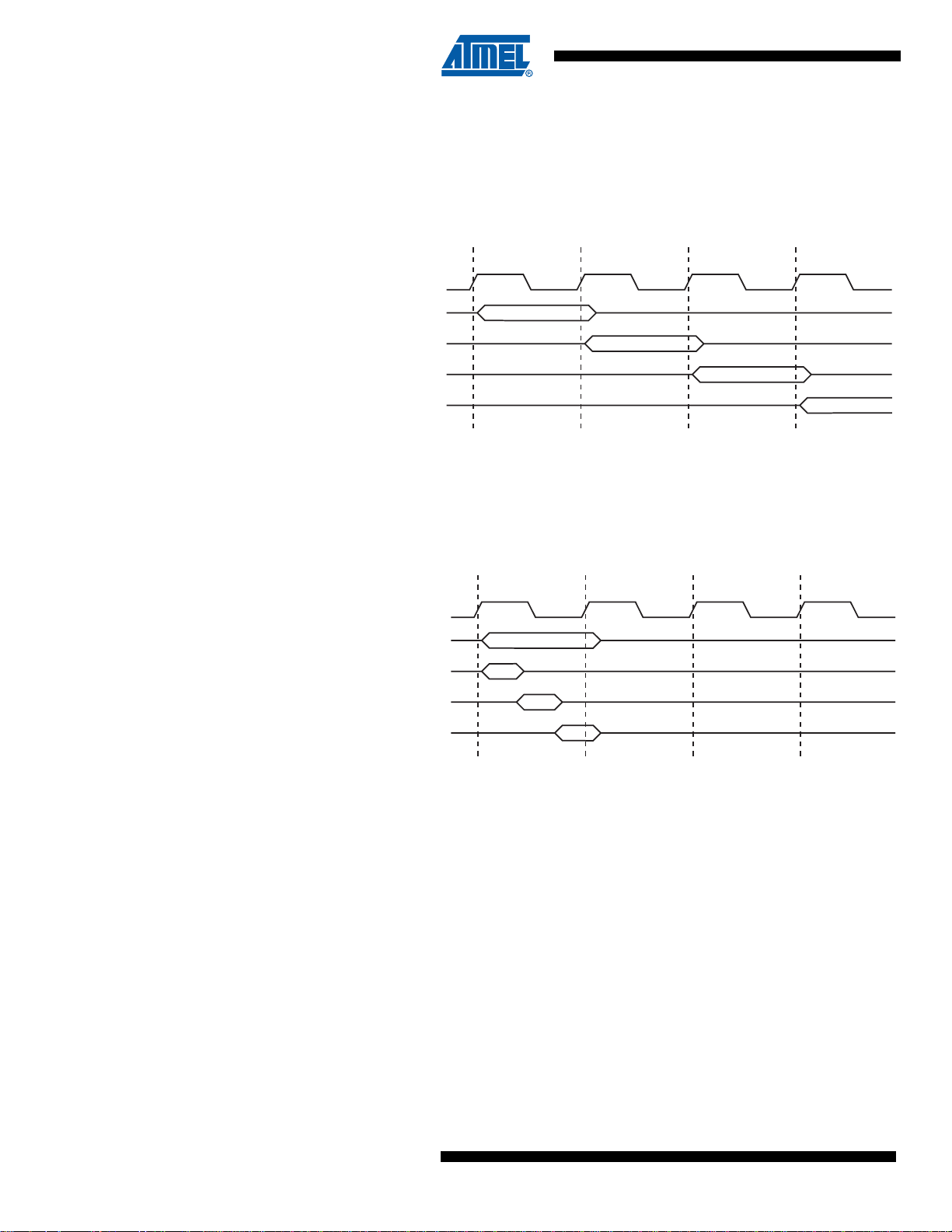
Figure 3-4 shows the parallel instructio n fetches an d instruc tion ex ecutions enable d by the Ha r-
2
T1 T2 T3 T4
T1 T2 T3 T4
vard architecture and th e fast- access Register File con cept. Thi s is the bas ic pipel ining conce pt
to obtain up to 1 MIPS per MHz with the cor respondi ng unique res ults for func tions per cos t,
functions per clocks, and functions per power-unit.
Figure 3-4. The Parallel Instruction Fetches and Instruction Executions
clk
CPU
1st Instruction Fetch
1st Instruction Execute
2nd Instruction Fetch
nd Instruction Execute
3rd Instruction Fetch
3rd Instruction Execute
4th Instruction Fetch
Figure 3- 5 shows the internal timing concept for the Register File. In a single clock cycle an ALU
operation using two regi ster ope rands is executed , and the result is stored bac k to the de stination register.
Figure 3-5. Single Cycle ALU Operation
Total Execution Time
egister Operands Fetch
ALU Operation Execute
Result Write Back
3.8 Reset and Interrupt Handling
The AVR provides several different interrupt sources. These interrupts and the separate Reset
Vector each have a separate program vector in the program memory space. All interrupts ar e
assigned individual enable bits which must be written logic one together with the Global Interrupt
Enable bit in the Status Re gister in or der to ena ble the int errupt. De pendin g on the Prog ram
Counter value, interrupts may be automatically disabled when Boot Lock bits BLB02 or BLB12
are programmed. This feature improves software security. See the section “Memory Program-
ming” on page 295 for details .
The lowest addresses in the p rogram memory space are by default defined as the Reset a nd
Interrupt Vectors. The complete list of vectors is shown in “Interrupts” on pag e 57. The list also
determines the priority levels of the different interrupts. The lower the address the higher is the
priority level. RESET has the hig hes t prior it y, and next is ANACOMP0 – the Analog Comparator
0 Interrupt. The Interr upt Ve ctor s can be moved to t he start of the B oot Flas h secti on by settin g
the IVSEL bit in the MCU Control Register (MCUCR). Refer to “Inte rrupts” on p age 5 7 for more
information. The Reset Vector can also be moved to the start of the Boot Flash section by pro-
clk
CPU
18
7647D–AVR–08/08
Page 19

gramming the BOOTRST Fuse, see “Boot Loader Support – Read-While-Write Self-
Programming ATmega16/32/64/M1/C1” on page 276.
3.8.1 Interrupt Behavior
When an interrupt occurs, the Global Interrupt Enable I-bit is cleared and all interrupts are disabled. The user softw are c an write lo gic one to the I-bit to enab le nes ted i nterrup ts. Al l ena bled
interrupts can then interrupt the current interrupt routine. The I-bit is automa tically set when a
Return from Interrupt instruction – RETI – is executed.
There are basically two types of interrupts. The first type is triggered by an event that sets the
interrupt flag. For these interrupts, the Program Counter is vectored to the actual Interrupt Vector
in order to execut e the int errupt ha ndlin g routine , and hardware clears the cor respon ding inte rrupt flag. Interrupt flags can also be cleared by writing a logic one to the flag bit position(s) to be
cleared. If an interrupt condition occurs while the corresponding interrupt enable bit is cleared,
the interrupt flag wi ll be set an d remembe red u ntil th e interr upt is enabl ed, or th e flag is c leared
by software. Similarly, if one or more interrupt conditions occur while the Global Interrupt Enable
bit is cleared, the c orrespond ing interru pt flag(s) wil l be set and reme mbered unti l the Globa l
Interrupt Enable bit is set, and will then be executed by order of priority.
The second type of interrupts will trigger as long as the interrupt condition is present. These
interrupts do not necessa rily hav e in ter rupt fl ags . If the interr up t con dit ion disapp ear s befo re the
interrupt is enabled, the interrupt will not be triggered.
ATmega16/32/64/M1/C1
When the AVR exits from an interrupt, it will always return to the main program and execute one
more instruction before any pending interrupt is served.
Note that the Status Register is not automatic ally stored when entering an in terrupt rou tine, nor
restored when returning from an interrupt routine. This must be handled by software.
When using the CLI instruct ion to disable interrupts, the interrupt s will be immedia tely disab led.
No interrupt will be executed after the CLI instruction, even if it occurs simultaneously with the
CLI instruction. The following example shows how this can be used to avoid interrupts during the
timed EEPROM write sequence..
Assembly Code Example
in r16, SREG ; store SREG value
cli ; disable interrupts during timed sequence
sbi EECR, EEMWE ; start EEPROM write
sbi EECR, EEWE
out SREG, r16 ; restore SREG value (I-bit)
C Code Example
char cSREG;
cSREG = SREG; /* store SREG value */
/* disable interrupts during timed sequence */
_CLI();
EECR |= (1<<EEMWE); /* start EEPROM write */
EECR |= (1<<EEWE);
SREG = cSREG; /* restore SREG value (I-bit) */
7647D–AVR–08/08
19
Page 20

ATmega16/32/64/M1/C1
When using the SEI instruction to enable interrupts, the instruction following SEI will be executed before any pending interrupts, as shown in this example.
Assembly Code Example
C Code Example
3.8.2 Interrupt Response Time
The interrupt execution response for all the enabled AVR interrupts is four clock cycles minimum. After four clock cycles the program vector address for the actual interrupt handling routine
is executed. During this four clock cycle pe riod , the Prog ram Co unter is pu shed o nto the Stack.
The vector is normally a jump to the interrupt routine, and this jump takes three clock cycles. If
an interrupt occurs during execution of a multi-cycle instruction, this instruction is completed
before the interrupt is served. If an interrupt occurs when the MCU is in sleep mode, the interrupt
execution response time is increased by four clock cycles. This increase comes in addition to the
start-up time from the selected sleep mode.
sei ; set Global Interrupt Enable
sleep; enter sleep, waiting for interrupt
; note: will enter sleep before any pending
; interrupt(s)
_SEI(); /* set Global Interrupt Enable */
_SLEEP(); /* enter sleep, waiting for interrupt */
/* note: will enter sleep before any pending interrupt(s) */
A return from an inter rupt handli ng routine takes four clock cycles. During the se four c lock
cycles, the Program Cou nter (two bytes ) is popped back fr om the Stack, the Sta ck Pointer is
incremented by two, and the I-bit in SREG is set.
20
7647D–AVR–08/08
Page 21

4. Memories
FF
Program Memory
This section describes the different memories in the ATmega16/32/64/M1/C1. The AVR architecture has two m ain memor y spaces , the Data Mem ory and the P rogram Me mory space. In
addition, the ATmeg a16/32/64/M 1/C1 fe atures an EEP ROM Memo ry for data stor age. All three
memory spaces are linear and regular.
4.1 In-System Reprogrammable Flash Program Memory
The ATmega16/32/64/M1 /C1 co ntai ns 16K/32K /64 K by tes On-chi p In-Sy ste m Reprog r amm abl e
Flash memory for p rogram storage . Sin ce all A VR i nstru ction s are 1 6 or 32 bit s wide , the Fl ash
is organized as 8K x 16 , 16K x 16 , 32K x 16. For software securit y, th e Flas h Pro gr am m emo ry
space is divided into two section s, Boo t Prog ram sec ti on and App li ca tio n Pro gram section.
The Flash memory has an endurance of at least 10,000 write/erase cycles. The
ATmega16/32/64/M1/C1 Program Counter (PC) is 14/15 bits wide, thus addressing the
8K/16K/32K progr am me mor y lo ca tio ns. The operation of Bo ot P ro gram section and associ ate d
Boot Lock bits for software protection are described in detail in “Boot Loader Support – Read-
While-Write Se lf-Pro gramm ing ATme ga16/3 2/64/M1 /C1” on pa ge 276. “Memory Programming”
on page 295 contains a detailed description on Flash programming in SPI or Parallel program-
ming mode.
Constant tables can be allocated within the entire program memory address space (see the LPM
– Load Program Memory.
ATmega16/32/64/M1/C1
Timing diagrams for instruction fetch and execution are presented in “Instruction Execution Tim-
ing” on page 17.
Figure 4-1. Program Memory Map
0x0000
Application Flash Section
7647D–AVR–08/08
Boot Flash Section
0x1FFF/0x3FFF/0x7
21
Page 22

ATmega16/32/64/M1/C1
4.2 SRAM Data Memory
0F
Figure 4-2 shows how the ATmega16/32/64/M1/C1 SRAM Memory is organized.
The ATmega16/32/64/M1/C1 is a complex microcontroller with more peripheral units than can
be supported within the 64 locations reserved in the Opcode for the IN and OUT instructions. For
the Extended I/O space from 0x60 - 0xFF in SRAM, only the ST/STS/STD and LD/LDS/LDD
instructions can be used.
The lower 2304 data memory locations address both the Register File, the I/O memory,
Extended I/O memory, an d the intern al data SRAM . The first 32 lo cations address the Register
File, the next 64 location the sta ndard I/O memory, then 160 locations of Exte nded I/ O memor y,
and the next 1024/2048/4096 locations address the internal data SRAM.
The five different addressing modes for the data memory cover: Direct, Indirect with Displacement, Indirect, Ind irect with Pre- decrement , and Indirect with Post-inc rement. In the Re gister
File, registers R26 to R31 feature the indirect addressing pointer registers.
The direct addressing reaches the entire data space.
The Indirect with Displacement mode reaches 63 address locations from the base address given
by the Y- or Z-register.
When using register indirect addressing modes with automatic pre-decr ement and post-incre-
ment, the address registers X, Y, and Z are decremented or incremented.
The 32 general purpose working registers, 64 I/O Registers, 160 Extended I/O Registers, and
the 1024/2048/4096 bytes of internal data SRAM in the ATmega16/32/64/M1/C1 are all accessible through all these addressing modes. The Register File is described in “General Purpose
Register File” on page 16.
Figure 4-2. Data Memory Map for 1024/2048/4096 Internal SRAM
4.2.1 SRAM Data Access Times
This section describes the general access timing concepts for internal memory access. The
internal data SRAM access is performed in two clk
Data Memory
32 Registers
64 I/O Registers
160 Ext I/O Reg.
Internal SRAM
(1024x8)
(2048x8)
(4096x8)
0x0000 - 0x001F
0x0020 - 0x005F
0x0060 - 0x00FF
0x0100
0x04FF/0x08FF/0x1
cycles as described in Figure 4-3.
CPU
22
7647D–AVR–08/08
Page 23
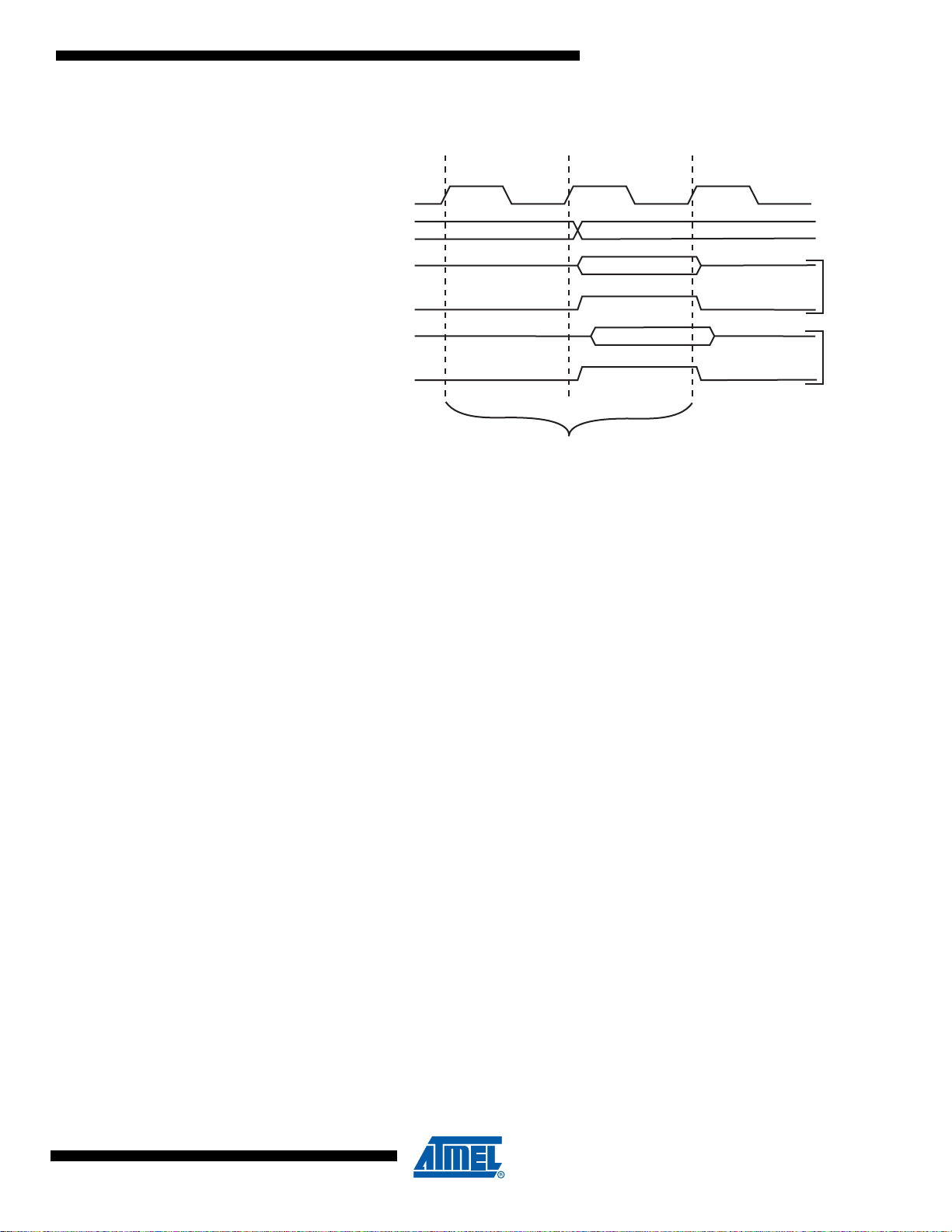
Figure 4-3. On-chip Data SRAM Access Cycles
A
T1 T2 T3
clk
CPU
ddress
Compute Address
Data
ATmega16/32/64/M1/C1
Address valid
4.3 EEPROM Data Memory
The ATmega16/32/64/M1/C1 contains 512/1024/2048 bytes of data EEPROM memory. It is
organized as a separate data space, in which single bytes can be read and written. The
EEPROM has an en duranc e of at least 100,000 wr ite/era se cycles. The access betwee n the
EEPROM and the CPU is described in the following, specifying the E EPROM Address Regi sters, the EEPROM Data Register, and the EEPROM Control Register.
For a detailed description of SPI and Parallel data downloading to the EEPROM, see “Serial
Downloading” on page 311 , and “Parallel Programming Parameters, Pin Mapping, and Commands” on page 299 respectively.
4.3.1 EEPROM Read/Write Access
The EEPROM Access Registers are accessible in the I/O space.
WR
Data
RD
Memory Access Instruction
Write
Read
Next Instruction
The write access time for the EEPROM is given in Table 4-2. A self-timing function, however,
lets the user software detect when the next byte can be written. If the user code contains instructions that write the EE PROM, some precau tions must be taken. In he avily filtered power
supplies, V
is likely to rise or fall slowly on power-up/down. This causes the device for some
CC
period of time to run at a vo ltag e lo wer tha n sp ec ifi ed as mi ni mum for the clo ck frequ enc y u se d.
See “Preventing EEPROM Corruption” on page 28.for details on how to avoid problems in these
situations.
In order to prevent unintentional EEPROM writes, a specific write procedure must be followed.
Refer to the description of the EEPROM Control Register for details on this.
When the EEPROM is read, the CPU is halted for four clock cycles before the next instruction is
executed. When the E EPROM is writ ten, the CPU i s halted for tw o clock cycles before t he nex t
instruction is execute d.
23
7647D–AVR–08/08
Page 24
ATmega16/32/64/M1/C1
4.3.2 The EEPROM Address Registers – EEARH and EEARL
Bit 15 14 13 12 11 10 9 8
– – – – – EEAR10 EEAR9 EEAR8 EEARH
EEAR7 EEAR6 EEAR5 EEAR4 EEAR3 EEAR2 EEAR1 EEAR0 EEARL
76543 2 10
Read/Write RRRRRR/WR/WR/W
R/W R/W R/W R/W R/W R/W R/W R/W
Initial Value 0 0 0 0 0 X X X
XXXXX X XX
• Bits 15.11 – Reserved Bits
These bits are reserved bits in the ATmega16/32/64/M1/C1 and will always read as zero.
• Bits 9..0 – EEAR10..0: EEPROM Address
The EEPROM Addre ss Registers – EEARH a nd EEARL specify the EEPR OM address in the
512/1024/2048 bytes EEPROM space. The EEPROM data bytes are addressed linearly
between 0 and 511/1023/2047. The initial value of EEAR is undefined. A proper value must be
written before the EEPROM may be accessed.
4.3.3 The EEPROM Data Register – EEDR
Bit 76543210
EEDR7 EEDR6 EEDR5 EEDR4 EEDR3 EEDR2 EEDR1 EEDR0 EEDR
Read/Write R/W R/W R/W R/W R/W R/W R/W R/W
Initial Value00000000
• Bits 7..0 – EEDR7.0: EEPROM Data
For the EEPROM write operation, the EEDR Register contains the data to be written to the
EEPROM in the address given by the EEAR Register. For the EEPROM read operation, the
EEDR contains the data read out from the EEPROM at the address given by EEAR.
4.3.4 The EEPROM Control Register – EECR
Bit 76543210
– – EEPM1 EEPM0 EERIE EEMWE EEWE EERE EECR
Read/Write R R R/W R/W R/W R/W R/W R/W
Initial Value 0 0 X X 0 0 X 0
• Bits 7..6 – Reserved Bits
These bits are reserved bits in the ATmega16/32/64/M1/C1 and will always read as zero.
• Bits 5..4 – EEPM1 and EEPM0: EEPROM Programming Mode Bits
The EEPROM Programming mode bit setting defines which programming action that will be triggered when writing EE W E. It is possible to prog ra m data i n o ne ato mic o peration (erase the old
value and program the new value) or to split the Erase and Write operations in two different
operations. Th e Programming ti mes for the diffe rent modes ar e shown in Tabl e 4-1. While
24
7647D–AVR–08/08
Page 25
ATmega16/32/64/M1/C1
EEWE is set, any write to EEPMn will be ignored . During rese t, the EEP Mn bits will be r eset to
0b00 unless the EEPROM is busy programming.
Table 4-1. EEPROM Mode Bits
Programming
EEPM1 EEPM0
0 0 3.4 ms Erase and Write in one operation (Atomic Operation)
0 1 1.8 ms Erase Only
1 0 1.8 ms Write Only
1 1 – Reserved for future use
• Bit 3 – EERIE: EEPROM Ready Interrupt Enable
Writing EERIE to one enables the EEPROM Ready Interrupt if the I bit in SREG is set. Writing
EERIE to zero disables the interrup t. The E EPROM Rea dy inter rup t generates a cons tant inte rrupt when EEWE is cleared. The interrupt will not be generated during EEPROM write or SPM.
• Bit 2 – EEMWE: EEPROM Master Write Enable
The EEMWE bit determines whether setting EEWE to one causes the EEPROM to be written.
When EEMWE is set, setting EEWE within four clock cycles will write data to the EEPROM at
the selected address If EEMWE is zero, setting EEWE will have no effect. When EEMWE has
been written to on e by soft ware, ha rdwar e cle ars th e bit to z ero aft er fo ur cl ock c ycles . See th e
description of the EEWE bit for an EEPROM write procedure.
• Bit 1 – EEWE: EEPROM Write Enable
Time Operation
The EEPROM Write Enable Signa l EEWE is the write strobe to the EEPROM. When address
and data are correctly set up, the EE WE bit must be written to one to write the value into the
EEPROM. The EEMWE bit mu st b e written to one befor e a log ical one is written to E EWE, otherwise no EEPROM write tak es pla ce . Th e follow ing procedure should be followe d when writing
the EEPROM (the order of steps 3 and 4 is not essential):
1. Wait until EEWE becomes zero.
2. Wait until SPMEN (Store Program Memory Enable) in SPMCSR (Store Program Memory
Control and Status Register) becomes zero.
3. Write new EEPROM address to EEAR (optional).
4. Write new EEPROM data to EEDR (optional).
5. Write a logical one to the EEMWE bit while writing a zero to EEWE in EECR.
6. Within four clock cycles after setting EEMWE, write a logical one to EEWE.
The EEPROM can not be programmed during a CPU write to the Flash memory. The software
must check that the Flash programming is completed before initiating a new EEPROM write.
Step 2 is only rele vant if the soft ware cont ains a Boo t Load er allow ing the CPU to progr am the
Flash. If the Flash is never being updat ed by the CPU, step 2 ca n be omi tted . See “Bo ot Loa der
Support – Read-While-Write Self-Programming ATmega16/32/64/M1/C1” on page 276 for
details about Boot programming.
Caution: An interrupt between step 5 and step 6 will ma ke the write cycle fail, since the
EEPROM Master Write E nable will time-out. If an i nterrupt routi ne accessi ng the EEPROM is
interrupting another EEPROM access, the EEAR or EEDR Register will be modified, causing the
interrupted EEPROM access to fail. It is recommended to have the Global Interrupt Flag cleared
during all the steps to avoid these problems.
7647D–AVR–08/08
25
Page 26

ATmega16/32/64/M1/C1
When the write access time has elapsed, the EEWE bit is cleared by hardware. The user software can poll this bit and wait for a zero before writing the next byte. When EEWE has been set,
the CPU is halted for two cycles before the next instruction is executed.
• Bit 0 – EERE: EEPROM Read Enable
The EEPROM Read Enable S ignal EE RE is the re ad strobe to the EE PROM. Whe n the corr ect
address is set up in the EEAR Register, the EERE bit must be written to a logic one to trigger the
EEPROM read. The EEPROM read access takes one instruction, and the requested data is
available immediatel y. When the EEPRO M is read, the CPU is halted for four cycles before the
next instruction is executed.
The user should poll the EEWE bit before starting the read operation. If a write operation is in
progress, it is neither possible to read the EEPROM, nor to change the EEAR Register.
The calibrated Osci llat or i s used t o tim e the EEP ROM acce sses. Table 4-2 lists the typi cal programming time for EEPROM access from the CPU.
Table 4-2. EEPROM Programming Time.
Symbol Number of Calibrated RC Oscillator Cycles Typ Programming Time
EEPROM write
(from CPU)
The following code examples show one assembly and on e C function for writin g to the
EEPROM. The examples assume that interrupts are controlled (e.g. by disabling interrupts globally) so that no interrupts will occur during execution of these functions. The examples also
assume that no Flash Boot Loader is present in the software. If such code is present, the
EEPROM write function must also wait for any ongoing SPM command to finish.
26368 3.3 ms
26
7647D–AVR–08/08
Page 27

ATmega16/32/64/M1/C1
Assembly Code Example
EEPROM_write:
; Wait for completion of previous write
sbic EECR,EEWE
rjmp EEPROM_write
; Set up address (r18:r17) in address register
out EEARH, r18
out EEARL, r17
; Write data (r16) to data register
out EEDR,r16
; Write logical one to EEMWE
sbi EECR,EEMWE
; Start eeprom write by setting EEWE
sbi EECR,EEWE
ret
C Code Example
void EEPROM_write (unsigned int uiAddress, unsigned char ucData)
{
/* Wait for completion of previous write */
while(EECR & (1<<EEWE))
;
/* Set up address and data registers */
EEAR = uiAddress;
EEDR = ucData;
/* Write logical one to EEMWE */
EECR |= (1<<EEMWE);
/* Start eeprom write by setting EEWE */
EECR |= (1<<EEWE);
}
7647D–AVR–08/08
27
Page 28

ATmega16/32/64/M1/C1
The next code e xampl es sho w ass embly and C funct ions for r eading the EEPR OM. Th e ex amples assume that interrupts are controlled so that no interrupts will occur during execution of
these functions.
Assembly Code Example
EEPROM_read:
; Wait for completion of previous write
sbic EECR,EEWE
rjmp EEPROM_read
; Set up address (r18:r17) in address register
out EEARH, r18
out EEARL, r17
; Start eeprom read by writing EERE
sbi EECR,EERE
; Read data from data register
in r16,EEDR
ret
C Code Example
unsigned char EEPROM_read(unsigned int uiAddress)
{
/* Wait for completion of previous write */
while(EECR & (1<<EEWE))
;
/* Set up address register */
EEAR = uiAddress;
/* Start eeprom read by writing EERE */
EECR |= (1<<EERE);
/* Return data from data register */
return EEDR;
}
4.3.5 Preventing EEPROM Corruption
During periods of low V
too low for the CPU and the EEPROM t o operate prop erly. These is sues are the s ame as for
board level systems using EEPROM, and the same design solutions should be applied.
An EEPROM data corruption can be caused by two situations when the voltage is too low. First,
a regular write sequence to the EEPROM requires a minimum voltage to operate correctly. Secondly, the CPU itself can execute instructions incorrectly, if the supply voltage is too low.
EEPROM data corruption can easily be avoided by following this design recommendation:
Keep the AVR RESET ac tive (low) du ring per iods o f insu ffici ent power supp ly vo ltage. Th is ca n
be done by enabling the internal Brown-ou t Detect or (BOD ). If the de tectio n leve l of the in terna l
BOD does not match the needed detection level, an external low V
be used. If a reset occurs while a write operation is in progr ess, the write ope ratio n will be completed provided that the power supply voltage is sufficient.
28
the EEPROM data can be corrupted because the supply v oltage is
CC,
reset Protection circuit can
CC
7647D–AVR–08/08
Page 29

4.4 I/O Memory
ATmega16/32/64/M1/C1
The I/O space definition of the ATmega16/32/64/M1/C1 is shown in “Register Summary” on
page 355.
All ATmega16/32/64/M1/C1 I/Os and peripherals are placed in the I/O space. All I/O locations
may be accessed by the LD/L DS/LDD an d ST/STS /STD i nstruc tions, tr ansferr ing data be tween
the 32 general pur pose work ing regis ters and the I/O space . I/O register s within the address
range 0x00 - 0x1F are d irectl y bit-ac cessi ble usi ng the S BI and CBI in structi ons. In these registers, the value of single bits can be checked by using the SBIS and SBIC instructions. Refer to
the instruction set section for more details. When using the I/O specific commands IN and OUT,
the I/O addresses 0x00 - 0x3F must be used. When addressing I/O registers as data space
using LD and ST instructions, 0x20 must be added to these addresses. The
ATmega16/32/64 /M1/C1 is a complex mi crocontrol ler with mor e periphera l units than ca n be
supported within the 64 location re served in Opcode for the IN and OUT ins tructions. For the
Extended I/O space from 0x60 - 0xFF in SRAM, only the ST/STS/STD and LD/LDS/LDD instructions can be used.
For compatibility with future devices, rese rved bits should be wr itten to zero if acces sed.
Reserved I/O memory addresses should never be written.
Some of the status flags are cleared by writing a logical one to them. Note that, unlike most other
AVR’s, the CBI and S BI inst ruction s will onl y operate on the spe cified bi t, and ca n theref ore be
used on registers con tai nin g s uch s tatus fl ags. T he CBI a nd S BI ins truc ti ons work with re gisters
0x00 to 0x1F only.
The I/O and peripherals control registers are explained in later sections.
4.5 General Purpose I/O Registers
The ATmega16/32/64 /M1/ C 1 con t ains fou r Gener al P urpos e I/O Re gis ters . T h ese regi s ter s ca n
be used for storing any information, and they are particularly useful for storing global variables
and status flags.
The General Purp ose I/O Reg isters, within the address range 0x00 - 0x1F, are directly b itaccessible using the SBI, CBI, SBIS, and SBIC instructions.
4.5.1 General Purpose I/O Register 0 – GPIOR0
Bit 76543210
GPIOR07 GPIOR06 GPIOR05 GPIOR04 GPIOR03 GPIOR02 GPIOR01 GPIOR00 GPIOR0
Read/Write R/W R/W R/W R/W R/W R/W R/W R/W
Initial Value00000000
4.5.2 General Purpose I/O Register 1 – GPIOR1
Bit 76543210
GPIOR17 GPIOR16 GPIOR15 GPIOR14 GPIOR13 GPIOR12 GPIOR11 GPIOR10 GPIOR1
Read/Write R/W R/W R/W R/W R/W R/W R/W R/W
Initial Value00000000
4.5.3 General Purpose I/O Register 2 – GPIOR2
Bit 76543210
GPIOR27 GPIOR26 GPIOR25 GPIOR24 GPIOR23 GPIOR22 GPIOR21 GPIOR20 GPIOR2
Read/Write R/W R/W R/W R/W R/W R/W R/W R/W
Initial Value00000000
7647D–AVR–08/08
29
Page 30
ATmega16/32/64/M1/C1
5. System Clock
5.1 Clock Systems and their Distribution
Figure 5- 1 presents the principal clock systems in the AVR and their distribution. All of the clocks
need not be active at a given time . In order to re duce power consu mption, the clocks to unuse d
modules can be halted by using different sleep modes, as described in “Power Management and
Sleep Modes” on page 41. The clock systems are detailed below.
Figure 5-1. Clock Distribution
Fast Peripherals
CLK
PLL
PLL Input
Multiplexer
General I/O
Modules
PLL
clk
I/O
ADC CPU Core RAM
clk
ADC
AVR Clock
Control Unit
Clock
Multiplexer
Source Clock
clk
CPU
clk
FLASH
Reset Logic
Watchdog Clock
Watchdog Timer
Watchdog
Oscillator
Flash and
EEPROM
5.1.1 CPU Clock – clk
CPU
The CPU clock is routed to parts of the system concerned with operation of the AVR core.
Examples of such module s are the General Purpo se Regis ter File , the Stat us Regi ster an d the
data memory holding the Stack Pointer. Ha lti ng the CP U c lo ck i nhi bi ts the co re fr om pe rfo r min g
general operations and calculations.
5.1.2 I/O Clock – clk
I/O
The I/O clock is used by the majority of the I/O modules, like Timer/Counters, SPI, UART. The
I/O clock is also used by the External Interrupt module, but note that some external interrupts
are detected by asynchronous logic, allowing such interrupts to be detected even if the I/O clock
is halted.
30
External Clock
(Crystal
Oscillator)
Calibrated RC
Oscillator
7647D–AVR–08/08
Page 31

ATmega16/32/64/M1/C1
5.1.3 Flash Clock – clk
The Flash clock controls operation of the Flash interface. The Flash clock is usually active simultaneously with the CPU clock.
5.1.4 PLL Clock – clk
The PLL clock allows the fast peripherals to be clocked directly from a 64/32 MHz clock. A 16
MHz clock is also derived for th e CPU.
5.1.5 ADC Clock – clk
The ADC is provided with a dedicate d cl oc k dom ain. T his allows hal tin g the CP U and I/O cloc ks
in order to reduce noise generated by digital circuitry. This gives more accurate ADC conversion
results.
5.2 Clock So urces
The device has the following clock source options, selectable by Flash Fuse bits as illustrated
Table 5-1. The clock from the selected source is input to the AVR clock generator, and routed to
the appropriate modules.
Table 5-1. Device Clocking Options Select
FLASH
PLL
ADC
(1)
Device Clocking Option System
Clock PLL Input
CKSEL3..0
E xternal Crystal/Ceramic Resonator E xt Osc RC Osc 1111 - 1000
PLL output divided by 4 : 16 MHz / PLL driven by External
Crystal/Ceramic Resonator
PLL output divided by 4 : 16 MHz / PLL driven by External
Crystal/Ceramic Resonator
Reserved N/A N/A 0110
Reserved N/A N/A 0111
PLL output divided by 4 : 16 MHz PLL / 4 RC Osc 0011
Calibrated Internal RC Oscillator RC Osc RC Osc 0010
PLL output divided by 4 : 16 MHz / PLL driven by External
clock
External Clock Ext Clk RC Osc 0000
Note: 1. For all fuses “1” means unprogrammed while “0” means program med.
2. Ext Osc : External Osc
3. RC Osc : Internal RC Oscillator
4. Ext Clk : External Clock Input
Ext Osc Ext Osc 0100
PLL / 4 Ext Osc 0101
PLL / 4 Ext Clk 0001
The various choices for each clocking option is given in the following sections. When the CPU
wakes up from Powe r-down or Power-sa ve, the se lected clo ck sourc e is used to ti me the star tup, ensuring stable Oscillator operation before instruction execution starts. When the CPU starts
from reset, there is an add iti ona l de lay al lo win g the p o wer to r ea ch a sta bl e le ve l be for e s tarting
normal operation. The Watchdog Oscillator is used for timing this real-time part of the start-up
time. The number of WDT Oscillator cycles used for each time-out is shown in Table 5-2. The
7647D–AVR–08/08
31
Page 32

ATmega16/32/64/M1/C1
frequency of the Watchdog Oscillator is voltage dependent as shown in “W atchdog Oscillator
2
1
Frequency vs. VCC” on page 345.
Table 5-2. Number of Watchdog Oscillator Cycles
Typ Time-out (VCC = 5.0V) Typ Time-out (VCC = 3.0V) Number of Cycles
4.1 ms 4.3 ms 4K (4,096)
65 ms 69 ms 64K (65,536)
5.3 Default Clock Source
The device is shipped with CKSEL = “0010”, SUT = “10”, and CKDIV8 programmed. The default
clock source setti ng is the Intern al RC O scill ator w ith lon gest star t-up ti me and an ini tial s ystem
clock prescaling of 8. This def ault setting ensur es that all users can make their desired clock
source setting using an In-System or Parall el pr ogram mer .
5.4 Low Power Crystal Oscillator
XTAL1 and XTAL2 are input and output, respectively, of an inverting amplifier which can be configured for use as an On-chip Oscillator, as shown in Figure 5-2. Either a quartz crystal or a
ceramic resonator may be used.
This Crystal Oscillator is a low power oscillator, with reduced voltage swing on the XTAL2 output. It gives the lowest power consumption, but is not capable of driving other clock inputs.
C1 and C2 should always be equal for both c rystals and reso nators. The optim al value of the
capacitors depends o n the crystal or resonator i n u se , the am oun t of str ay cap ac itan ce , an d th e
electromagneti c noise of the environme nt. Some in itial guid elines for choosing capacitors for
use with crystals are given in Table 5-3. For ceramic resonators, the capacitor values given by
the manufacturer shoul d be used. For more in formati on on how to choose capacitors and other
details on Oscillator operation, refer to the Multi-purpose Oscillator Application Note.
Figure 5-2. Crystal Oscillator Connections
C2
C1
XTAL
XTAL
GND
The Oscillator can operate in three different modes, each optimized for a specific frequency
range. The operating mode is selected by the fuses CKSEL3..1 as shown in Table 5-3.
Table 5-3. Crystal Oscillator Operating Modes
Recommended Range for Capacitors C1 and
C2 for Use with Crystals (pF)
CKSEL3..1 Frequency Range
(2)
100
0.4 - 0.9 –
(1)
(MHz)
32
7647D–AVR–08/08
Page 33

Table 5-3. Crystal Oscillator Operating Modes
ATmega16/32/64/M1/C1
CKSEL3..1 Frequency Range
101 0.9 - 3.0 12 - 22
110 3.0 - 8.0 12 - 22
111 8.0 -16.0 12 - 22
Notes: 1. The frequency ranges are preliminary values. Actual values are TBD.
2. This option should not be used with crystals, only with ceramic resonators.
(1)
(MHz)
Recommended Range for Capacitors C1 and
C2 for Use with Crystals (pF)
The CKSEL0 Fuse toge the r with th e S UT 1..0 Fu ses select the start-up tim es as s ho wn in Table
5-4.
Table 5-4. Start-up Times for the Oscillator Clock Selection
Start-up Time from
Power-down and
CKSEL0 SUT1..0
0 00 258 CK
0 01 258 CK
010 1K CK
011 1K CK
Power-save
(1)
(1)
(2)
(2)
Additional Delay
from Reset
= 5.0V) Recommended Usage
(V
CC
14CK + 4.1 ms
14CK + 65 ms
14CK
14CK + 4.1 ms
Ceramic resonator, fast
rising power
Ceramic resonator , slo wly
rising power
Ceramic resonator, BOD
enabled
Ceramic resonator, fast
rising power
100 1K CK
1 01 16K CK 14CK
1 10 16K CK 14CK + 4.1 ms
1 11 16K CK 14CK + 65 ms
Notes: 1. These options shoul d o nl y b e u se d w h en not ope rating close to the maximum frequency o f th e
device, and only if frequency stability at start-up is not important for the application. These
options are not suitable for crystals.
2. These options are intended for use with ceramic resonators and will ensure frequency stability
at start-up. They can also be used with crystals when not operating close to the maximum frequency of the device, and if frequency stability at start-up is not important for the application.
5.5 Calibrated Internal RC Oscillator
By default, the Internal RC OScillator provides an approximate 8.0 MHz clock. Though voltage
and temperature dependent, this clock can be very accurately calibrated by the user. The device
is shipped with the CKDIV8 Fuse programmed. See “System Clock Prescaler” on pa ge 38 for
more details.
This clock may be selected as the system clock by programming the CKSEL Fuses as shown in
Table 5-1. If selecte d, it will operate with no ext er nal comp one nts . Du ri ng res et, h ardware loads
the pre-programmed calibration value into the OSCCAL Register and thereby automatically cal-
(2)
14CK + 65 ms
Ceramic resonator , slo wly
rising power
Crystal Oscillator, BOD
enabled
Crystal Oscillator, fast
rising power
Crystal Oscillator, slowly
rising power
7647D–AVR–08/08
33
Page 34

ATmega16/32/64/M1/C1
ibrates the RC Oscillator. The accuracy of this calibration is shown as Factory calibration in
Table 26-1 on page 318.
By changing the OSCCAL registe r from SW , see “Oscillator Calibration Register – OSCCAL” on
page 34, it is pos sible to ge t a higher calibr ation ac curac y than by us ing the fac tory ca librati on.
The accur acy o f t his cal ibr atio n is sh ow n as Use r c ali brat ion in “Clock Characteristics” on page
318.
When this Oscillator is used as the chip clock, the Watchdog Oscillator will still be used for the
Watchdog Timer and for the Re se t Time- o ut. For mor e in forma t io n on the pre- progr am med cal ibration value, see the section .
Table 5-5. Internal Calibrated RC Oscillator Operating Modes
Frequency Range (MHz) CKSEL3..0
7.3 - 8.1 0010
Notes: 1. The device is shipped with this option selected.
2. If 8 MHz frequency exceeds the specification of the device (depends on V
Fuse can be programmed in order to divide the internal frequency by 8.
(1)(2)
), the CKDIV8
CC
When this Oscillator is selected, start-up times are determined by the SUT Fuses as shown in
Table 5-6 on page 34.
Table 5-6. Start-up times for the internal calibrated RC Oscillator clock selection
Start-up Time from Power-
Power Conditions
BOD enabled 6 CK 14CK
Fast rising power 6 CK 14CK + 4.1 ms 01
Slowly rising power 6 CK 14CK + 65 ms
Note: 1. If the RSTDISBL fuse is programmed, this start-up time will be increased to
14CK + 4.1 ms to ensure programming mode can be entered.
The device is shipped with this option selected.
2.
down and Power-save
Reserved 11
Additional Delay from
Reset (VCC = 5.0V) SUT1..0
(1)
(2)
00
10
5.5.1 Oscillator Calibration Register – OSCCAL
Bit 76543210
Read/Write R/W R/W R/W R/W R/W R/W R/W R/W
Initial Value Device Specific Calibration Value
• Bits 7..0 – CAL7..0: Oscillator Calibration Value
The Oscillator Calibration Register is used to trim the Calibrated Internal RC Oscillator to
remove process variations from the oscillator frequency. The factory-calibrated value is automatically written to th is regi ste r dur in g ch ip r es et, g iv ing an oscillator frequenc y o f 8.0 MHz a t 25° C.
The application software can write this register to change the oscillator frequency. The oscillator
can be calibrated to any frequ ency in the range 7.3 - 8.1 MHz within ±1% accuracy . Calibratio n
outside that range is not guaranteed.
Note that this oscillator is used to time EEPROM and Flash write accesses, and these write
times will be affec ted acco rdin gly. I f the E EPROM or Fla sh are writte n, do n ot calib rate t o more
than 8.8 MHz. Otherwise, the EEPROM or Flash write may fail.
34
CAL7 CAL6 CAL5 CAL4 CAL3 CAL2 CAL1 CAL0 OSCCAL
7647D–AVR–08/08
Page 35

5.6 PLL
5.6.1 Internal PLL
ATmega16/32/64/M1/C1
The CAL7 bit determines the range of operation for the oscillator. Setting this bit to 0 gives the
lowest frequency range, setting this bit to 1 gives the highest frequency range. The two frequency ranges are overlapping, i n other words a setting of OSCCAL = 0x7F gives a higher
frequency t han OSCCAL = 0x80.
The CAL6..0 bits are u sed to tune the frequency withi n the selecte d range. A se tting of 0x00
gives the lowest frequency in that range, and a setting of 0x7F gives the highest frequency in the
range. Incrementing CAL6..0 by 1 will give a frequency increment of less than 2% in the frequency range 7.3 - 8.1 MHz.
The internal PLL in ATmega16/32/64/M1/C1 generates a clock frequency that is 64x multiplied
from its nominal 1 MHz input. The source of the 1 MHz PLL input clock can be:
• the output of the internal RC Oscillator divided by 8.
• the output of the Crystal Oscillator divided by 8
• the external clock divided by 8
See the Figure 5-3 on page 36.
When the PLL is locked on the RC Oscillator, adjusting the RC Oscillator via OSCCAL Register,
will also modify the PLL clock output. However, even if the possibly divided RC Oscillator is
taken to a higher frequency than 8 M Hz, the PLL output c lock frequency satura tes at 70 MHz
(worst case) and r ema ins o sc illa tin g at the maximum frequenc y . It sh oul d b e no ted that the PLL
in this case is not locked any more with its 1MHz source clock.
Therefore it is recomme nded not to take the OSCCAL adjustments to a higher frequency than 8
MHz in order to keep the PLL in the correct operating range.
The internal PLL is enabled only when the PLLE bit in the register PLLCSR is set. The bit
PLOCK from the register PLLCSR is set when PLL is locked.
Both internal 8 MHz RC Oscillator, Crystal Oscillator and PLL are switched off in Power-down
and Standby sleep modes.
.
Table 5-7. Start-up Times when the PLL is selected as system clock
CKSEL
3..0 SUT1..0
0011
RC Osc
00 1K CK 14CK
01 1K CK 14CK + 4 ms
10 1K CK 14CK + 64 ms
11 16K CK 14CK
Start-up Time from Power-down
and Power-save
Additional Delay from Reset
(V
= 5.0V)
CC
7647D–AVR–08/08
0101
Ext Osc
00 1K CK 14CK
01 1K CK 14CK + 4 ms
10 16K CK 14CK + 4 ms
11 16K CK 14CK + 64 ms
35
Page 36

ATmega16/32/64/M1/C1
Table 5-7. Start-up Times when the PLL is selected as system clock
OSCCAL
CKSEL
3..0 SUT1..0
0001
Ext Clk
00 6 CK
01 6 CK
10 6 CK
Start-up Time from Power-down
and Power-save
(1)
(2)
(3)
Additional Delay from Reset
= 5.0V)
(V
CC
14CK
14CK + 4 ms
14CK + 64 ms
11 Reserved
1. This value do not provide a proper restart ; do not use PD in this clock scheme
2. This value do not provide a proper restart ; do not use PD in this clock scheme
3. This value do not provide a proper restart ; do not use PD in this clock scheme
Figure 5-3. PLL Clocking System
CKSEL3..0
PLLE
Lock
Detector
PLLF
PLOCK
RC OSCILLATOR
XTAL1
XTAL2
8 MHz
OSCILLATORS
DIVIDE
BY 8
PLL
64x
DIVIDE
BY 2
DIVIDE
BY 4
CLK
PLL
CK
SOURCE
36
7647D–AVR–08/08
Page 37

5.6.2 PLL Control and Status Register – PLLCSR
2
1
E
Bit 76543210
$29 ($29) – – – – – PLLF PLLE PLOCK PLLCSR
Read/Write R R R R R R/W R/W R
Initial Value 0 0 0 0 0 0 0/1 0
• Bit 7..3 – Res: Reserved Bits
These bits are reserved bits in the ATmega16/32/64/M1/C1 and always read as zero.
• Bit 2 – PLLF: PLL Factor
The PLLF bit is used to select the division factor of the PLL.
If PLLF is set, the PLL output is 64MHz.
If PLLF is clear, the PLL output is 32MHz.
• Bit 1 – PLLE: PLL Enable
When the PLLE is se t, the PLL is started and if not yet star ted the internal RC Oscillator is
started as PLL refer enc e cl ock. If P LL is selected as a sy st em cloc k sour c e th e v alue for th is bi t
is always 1.
• Bit 0 – PLOCK: PLL Lock Detector
When the PLOCK bit is set, the PLL is locked to the reference clock, and it is safe to enable
CLK
for Fast Peripherals. After the PLL is enabled, it takes about 100 ms for the PLL to lock.
PLL
ATmega16/32/64/M1/C1
5.7 128 kHz Internal Oscillator
The 128 kHz internal Oscillator is a low power Oscillator providing a clock of 128 kHz. The frequency is nominal at 3V and 25⋅C. This clock is used by the Watchdog Oscillator.
5.8 External Clock
To drive the devic e from an extern al clock source , XTAL 1 should be drive n as show n in Figure
5-4. To run the device on an external clock, the CKSEL Fuses must be programmed to “0000”.
Figure 5-4. External Clock Drive Configuration
Table 5-8. External Clock Frequency
CKSEL3..0 Frequency Range
NC
xternal
Clock
Signal
XTAL
XTAL
GND
0000 0 - 16 MHz
37
7647D–AVR–08/08
Page 38

ATmega16/32/64/M1/C1
When this clock source is selected, start-up times are determined by the SUT Fuses as shown in
Table 5-9.
Table 5-9. Start-up Times for the External Clock Selection
SUT1..0
00 6 CK 14CK BOD enabled
01 6 CK 14CK + 4.1 ms Fast rising power
10 6 CK 14CK + 65 ms Slowly rising power
11 Reserved
When applying an external clock, it is required to avoid sudden changes in the applied clock frequency to ensure stable operation of the MCU. A variation in frequency of more than 2% from
one clock cycle to the next can lead to unpredictable behavior. It is required to ensure that the
MCU is kept in Reset during such changes in the clock frequency.
Note that th e Syst em Cl oc k Pres cale r can be us ed t o impl eme nt ru n-t ime chan ges of th e int ern al
clock frequency while still ensuring stable operation. Refer to “System Clo ck Prescaler” on page
38 for details.
5.9 Clock Output Buffer
When the CKOUT Fuse is programmed, the system Clock will be output on CLKO. This mode is
suitable when chip clock is used to drive other circuits on the system. The clock will be output
also during reset and the n ormal o peration o f I/O pi n will be overridde n when th e fuse i s programmed. Any clock source, including internal RC Oscillator, can be selected when CLKO
serves as clock outpu t. If t he S y ste m Cl ock P r es ca ler i s used, i t i s t he d iv ided s y ste m clo ck th at
is output (CKOUT Fuse programmed).
Start-up Time from Power-
down and Power-save
Additional Delay from
Reset (VCC = 5.0V) Recommended Usage
5.10 System Clock Prescaler
The ATmega16/32/ 64/M1/C 1 sy stem clock can be d ivided by s etting the Clock Pres cale Register – CLKPR. This feature can be used to decrease power consumption when the requirement
for processing power is low. T his can b e used with al l clo ck sour ce options , and it wi ll affe ct the
clock frequenc y of the CPU and a ll synchr onous periph eral s. clk
are divided by a factor as shown in Table 5-10.
When switching between prescaler setti ngs, the System Clock Prescaler ensures that no
glitches occurs in the clock system. It also ensures that no intermediate frequency is higher than
neither the clock frequency corresponding to the previous setting, nor the clock frequency corresponding to the new setting. The ripple counter that implements the prescaler runs at the
frequency of the undivided clock, which may be faster than the CPU's clock frequency. Hence, it
is not possible to determine the state of the prescaler - even if it were readable, and the exact
time it takes to switch from one clo ck div isi on to the other can not be exa ctly pr ed icted. From the
time the CLKPS values are written, it takes between T1 + T2 and T1 + 2 * T 2 before the new
clock frequency is active. In this interval, 2 active clock edges are produced. Here, T1 is the previous clock period, and T2 is the period corresponding to the new prescaler setting.
To avoid unintentional changes of clock frequency, a special write procedure must be followed
to change the CLKPS bits:
I/O
, clk
ADC
, clk
, and clk
CPU
FLASH
38
7647D–AVR–08/08
Page 39
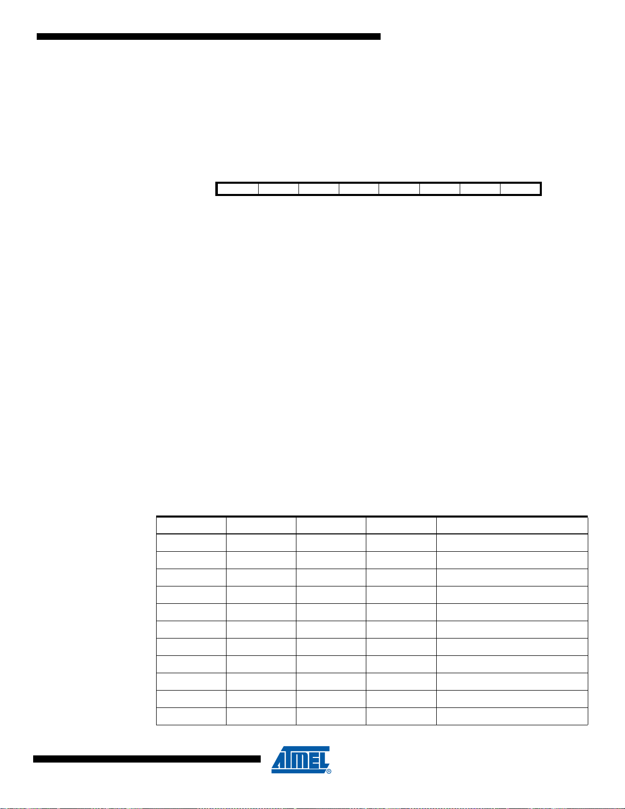
1. Write the Clock Prescaler Change Enable (CLKPCE) bit to one and all other bits in
CLKPR to zero.
2. Within four cycles, write the desired value to CLKPS while writing a zero to CLKPCE.
Interrupts must be disabled when changing prescaler setting to make sure the write procedure is
not interrupted.
5.10.1 Clock Prescaler Register – CLKPR
Bit 76543210
CLKPCE – – – CLKPS3 CLKPS2 CLKPS1 CLKPS0 CLKPR
Read/Write R/W R R R R/W R/W R/W R/W
Initial Value 0 0 0 0 See Bit Description
• Bit 7 – CLKPCE: Clock Prescaler Change Enable
The CLKPCE bit must be written to logic one to enable change of the CLKPS bits. The CLKPCE
bit is only updated when the other bits in CLKPR are simultaniosly written to zero. CLKPCE is
cleared by hardware four cycle s after it is writt en or wh en CLKP S bit s are writte n. Rewrit ing the
CLKPCE bit within this tim e-out period does neither extend the time-out period , nor clear the
CLKPCE bit.
• Bits 3..0 – CLKPS3..0: Clock Prescaler Select Bits 3 - 0
These bits define the division factor between the selected clock source and the internal system
clock. These bit s can be writt en run-time to vary the clock freque ncy to sui t the applic ation
requirements. As the divider divides the master clock input to the MCU, the speed of all synchronous peripherals is reduced when a division factor is used. The division factors are given in
Table 5-10.
ATmega16/32/64/M1/C1
The CKDIV8 Fuse de termine s the initi al value of th e CLKPS bits. If C KDIV8 is un progra mmed,
the CLKPS bits wil l be reset to “0000” . If CKDIV8 is pro grammed, CLKP S bits are reset to
“0011”, giving a division factor of 8 at start up. This feature shou ld be used if the sele cted clock
source has a higher frequency than the maximum frequency of the device at the present operating conditions. Note that any value can be written to the CLKPS bits regardless of the CKDIV8
Fuse setting. The Application software must ensure that a sufficient division factor is chosen if
the selcted clock source has a higher frequency than the max imum frequency of the device at
the present operating conditions. The device is shipped with the CKDIV8 Fuse programmed.
Table 5-10. Clock Prescaler Select
CLKPS3 CLKPS2 CLKPS1 CLKPS0 Clock Division Factor
0000 1
0001 2
0010 4
0011 8
0100 16
0101 32
0110 64
0111 128
1000 256
1001 Reserved
7647D–AVR–08/08
1010 Reserved
39
Page 40

ATmega16/32/64/M1/C1
Table 5-10. Clock Prescaler Select
CLKPS3 CLKPS2 CLKPS1 CLKPS0 Clock Division Factor
1011 Reserved
1100 Reserved
1101 Reserved
1110 Reserved
1111 Reserved
40
7647D–AVR–08/08
Page 41
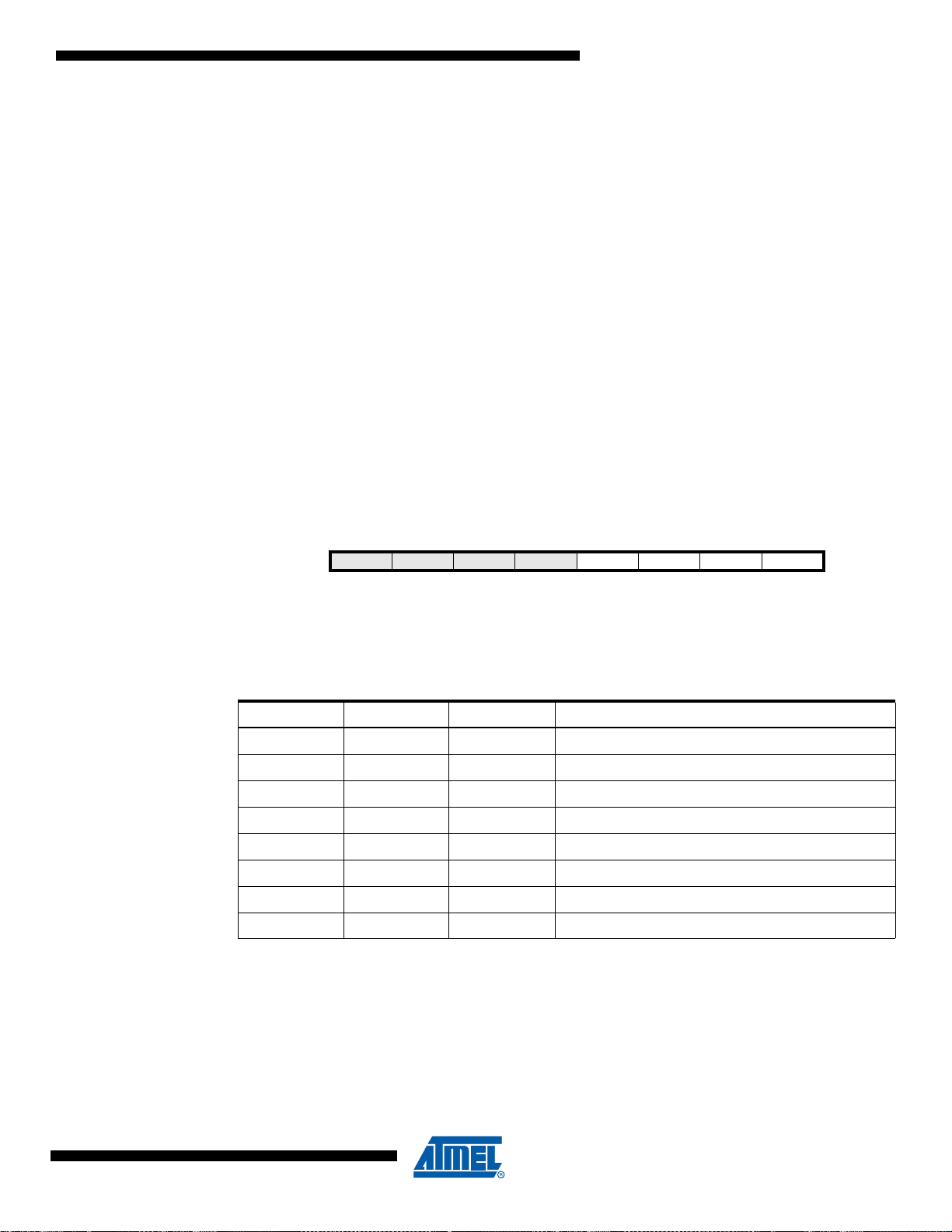
6. Power Management and Sleep Modes
Sleep modes enable the application to shut down unused modules in the MCU, thereby saving
power. The AVR provides various sleep modes allowing the user to tailor the power consumption to the application’s requirements.
To enter any of the five sleep modes, th e SE bit in SMCR m ust be written to lo gic one and a
SLEEP instruction must be executed. The SM2, SM1, and SM0 bits in the SMCR Register select
which sleep mode (Idle, ADC Noise Reduction, Power-down, Power-save, or Standby) will be
activated by the SLEEP instruction. See Table 6-1 for a summary. If an enabled interrupt occurs
while the MCU is in a sleep mode, the MCU wakes up. The MCU is then halted for four cycles in
addition to the start-up time, executes the interrupt routine, and resumes execution from the
instruction following SLEEP . The conte nts of the registe r file and SRAM are unal tered when the
device wakes up fro m sleep. If a reset oc curs duri ng sleep m ode, th e MCU wakes u p and executes from the Reset Vector.
Figure 5-1 on page 30 pr es ents t he different clock system s in the A T meg a16 /32/6 4/M 1/C1 , an d
their distribution. The figure is helpful in selecting an appropriate sleep mode.
6.1 Sleep Mode Control Register
6.1.1 Sleep Mode Control Register – SMCR
ATmega16/32/64/M1/C1
The Sleep Mode Control Register contains control bits for power management.
Bit 76543210
– – – – SM2 SM1 SM0 SE SMCR
Read/Write R R R R R/W R/W R/W R/W
Initial Value 0 0 0 0 0 0 0 0
• Bits 3..1 – SM2..0: Sleep Mode Select Bits 2, 1, and 0
These bits select between the five available sleep modes as shown in Table 6-1.
Table 6-1. Sleep Mode Select
SM2 SM1 SM0 Sleep Mode
000Idle
0 0 1 ADC Noise Reductio n
0 1 0 Power-down
0 1 1 Reserved
1 0 0 Reserved
1 0 1 Reserved
1 1 0 Standby
1 1 1 Reserved
Note: 1. Standby mode is only recommended for use with external crystals or resonators.
(1)
• Bit 1 – SE: Sleep Enable
7647D–AVR–08/08
The SE bit must be written to logic one to make the MCU enter the sleep mode when the SLEEP
instruction is executed. To avoid the MCU entering the sleep mode unless it is the programmer’s
purpose, it is recommended to write the Sleep Enable (SE) bit to one just before the execution of
the SLEEP instruction and to clear it immediately after waking up.
41
Page 42

ATmega16/32/64/M1/C1
6.2 Idle Mode
When the SM2 ..0 bits are written t o 000, the SLEEP in struction makes the MCU enter Idle
mode, stopping the CPU but allowing SPI, UART, Analog Comparator, ADC, Timer/Counters,
Watchdog, and the interrupt system to continue operating. This sleep mode basically halt clk
and clk
, while allowing the other clocks to run.
FLASH
Idle mode enables the MCU to wake up from external triggered interrupts as well as internal
ones like the Timer Overflow and UART Transmit Complete interrupts. If wake-up from the Analog Comparator interrupt is not required, the Analog Comparator can be powered down by
setting the ACD bit in the Analog Comparator Control and Status Register – ACSR. This will
reduce power consumption in Idle mode. If the ADC is enabled, a conversion starts automatically when this mode is entered.
6.3 ADC Noise Reduction Mode
When the SM2..0 bits are written to 001, the SLEEP instruction makes the MCU enter ADC
Noise Reduction mode, stopping the CP U but allowing the AD C, the External Inter rupts,
Timer/Counter (if their clock source is external - T0 or T1) and the Watc hdog to continue
operating (if enabled) . Thi s s lee p mo de ba si ca ll y ha lts cl k
the other clocks to run.
This improves the noi se envi ronment fo r the ADC, enablin g higher re solution measurem ents. If
the ADC is enabled, a conversion starts automatically when this mode is entered. Apart from the
ADC Conversion Complete interrupt, only an External Reset, a Watchdog Reset, a Brown-out
Reset, a Timer/Counter inte rrupt, an SPM/E EPROM r eady in terrupt, a n Exte rnal Level Interru pt
on INT3:0 can wake up the MCU from ADC Noise Reduction mode.
I/O
, clk
CPU
, and clk
, while allowing
FLASH
CPU
6.4 Power-down Mode
When the SM2..0 bits are written to 010, the SLEEP instruction makes the MCU enter Powerdown mode. In this mode, the External Oscillator is stopped, while the External Interrupts and
the Watchdog co ntinue oper ating (if en abled). Onl y an Externa l Reset, a Watc hdog Reset , a
Brown-out Reset, a PSC Interr upt, an Exter nal Lev el In ter rupt on INT3 :0 ca n wake up the MCU.
This sleep mode basically halts all generated clocks, allowing operation of asynchronous modules only.
Note that if a level triggered in terrupt is used for wake- up from Po wer-down mode, the cha nged
level must be held for some tim e to wak e up the MC U. R efer to “External Interrupts” on page 83
for details.
When waking up from Power-down mode, there is a del ay from the wake-up c ondition occurs
until the wake-up becomes effective. This all ows the clock to resta rt and beco me st able after
having been stopp ed. The wake -up period is defined by the same CK SEL fuse s that define th e
Reset Time-out period, as described in “Clock Sources” on page 31.
6.5 Standby Mode
When the SM2..0 bits are 110 and an external crystal/resonator clock option is selected, the
SLEEP instruc tion make s th e MCU enter Sta ndby mode. Thi s m ode i s iden tica l to Power -do wn
42
7647D–AVR–08/08
Page 43

ATmega16/32/64/M1/C1
with the excepti on tha t th e Osc illat or i s k ept r unning. From Standby mode , th e dev ic e wakes u p
in six clock cycles.
Table 6-2. Active Clock Domains and Wake-up Sources in the Different Sleep Modes.
Oscillator
Active Clock Domains
s Wake-up Sources
Sleep
Mode
Idle X X X X X X X X X X
ADC
Noise
Reduction
Powerdown
Standby
(1)
Notes: 1. Only recommended with external crystal or resonator selected as clock source.
2. Only level interrupt.
6.6 Power Reduction Register
The Power Reduction Register, PRR, provides a method to stop the clock to individual peripherals to reduce power consumption. The current state of the peripheral is frozen and the I/O
registers can n ot be read or wri tten. Re sour ces used by the p erip heral wh en st opping th e clock
will remain occupied, hence the peripheral should in most cases be disabled before stopping the
clock. Waking up a module, which is done by clearing the bit in PRR, puts the module in the
same state as before shutdown.
A full predictible behaviour of a peripheral is not guaranteed during and after a cycle of stopping
and starting of it s c lock. So i ts r eco mmend ed to sto p a peri phera l be fore stop ping its c lock wit h
PRR register.
CPU
clk
FLASH
clk
IO
clk
ADC
clk
PLL
clk
Main Clock
Source Enabled
XX X X
XX
INT3..0
PSC
Ready
ADC
WDT
OtherI/O
SPM/EEPROM
(2)
(2)
X
(2)
XXXX
X
X
Module shutdown can be used in Idl e mode and A ctive mode to signific antly redu ce the over all
power consumption. In all other sleep modes, the clock is already stopped.
6.6.1 Power Reduction Register - PRR
Bit 765432 1 0
- PRCAN PRPSC
Read/Write R R/W R/W R/W R/W R/W R/W R/W
Initial Value 0 0 0 0 0 0 0 0
• Bit 7 - Res: Reserved Bit
This bit is unused bit in the ATmega16/32/64/M1/C1, and will always read as zero.
• Bit 6 - PRCAN: Power Reduction CAN
Writing a logic one to th is bit redu ces the c onsump tion of the CAN by stoppi ng the clo ck to this
module. When waking up the CAN again, the CAN should be re initialized to ensure proper
operation.
• Bit 5 - PRPSC: Power Reduction PSC
7647D–AVR–08/08
PRTIM1 PRTIM0 PRSPI PRLIN PRADC PRR
43
Page 44

ATmega16/32/64/M1/C1
Writing a log ic on e to th is b it r edu ces the con sum ptio n of t he P SC by stop ping the cl ock to this
module. When waking up the PSC agai n, the PSC should b e re initialized to en sure proper
operation.
• Bit 4 - PRTIM1: Power Reduction Timer/Counter1
Writing a logic one to this bit reduces the consumption of the Timer/Counter1 module. When the
Timer/Counter1 is enabled, operation will continue like before the setting of this bit.
• Bit 3 - PRTIM0: Power Reduction Timer/Counter0
Writing a logic one to this bit reduces the consumption of the Timer/Counter0 module. When the
Timer/Counter0 is enabled, operation will continue like before the setting of this bit.
• Bit 2 - PRSPI: Power Reduction Serial Peripheral Interface
Writing a logic one to this bit reduces the consumption of the Serial Peripheral Interface by stopping the clock to this mo dule. W hen waki ng up the SPI agai n, the SP I shoul d be re ini tialized to
ensure proper operation.
• Bit 1 - PRLIN: Power Reduction LIN
Writing a logic one to this bit reduces the consumption of the UART controller by stopping the
clock to this module. When waking up the UART controller again, the UART controller should be
re initialized to ensure proper operation.
• Bit 0 - PRADC: Power Reduction ADC
Writing a logic on e to this bit re duces the c onsump tion of the ADC by stop ping the clo ck to this
module. The ADC must be disabled before using this function. The analog comparator cannot
use the ADC input MUX when the clock of ADC is stopped.
6.7 Minimizing Power Consumption
There are several issues to c ons id er when tr yi ng to min imiz e the pow er con sumpti on i n an AV R
controlled system. In gener al, slee p modes shou ld be u sed as much as poss ible , and the sleep
mode should be selected so that as few as possible of the device’s functions are operating. All
functions not needed sho uld be disa bled. In part icular, the following modul es may nee d specia l
consideration when trying to achieve the lowest possible power consumption.
6.7.1 Analog to Digital Converter
If enabled, the ADC will be enable d in a ll s leep mode s. T o save power, the A DC shou ld be disabled before entering any sleep mode. When the ADC is turned off and on again, the next
conversion will be an extended conversion. Refer to “Analog to Digital Converter - ADC” on page
228 for details on ADC operation.
6.7.2 Analog Comparator
When entering Idle mode, the Analog Comparator should be disabled if not used. When entering
ADC Noise Reduction mod e, th e A nal og Co mpa rator s hou ld b e di sabl ed. I n oth er sl ee p mo des ,
the Analog Comparator is automatically disabled. However, if the Analog Comparator is set up
to use the Internal Volta ge Re fer ence a s i nput , the A na log Comp arator should be disabled in al l
sleep modes. Otherwise, the Internal Voltage Reference will be enabled, independent of sleep
mode. Refer to “ Analog Co mparator ” on page 260 fo r details on how to conf igure the Ana log
Comparator.
44
7647D–AVR–08/08
Page 45

6.7.3 Brown-out Detector
If the Brown-out Detector is not needed by the application, this module should be turned off. If
the Brown-out Detector is enabl ed by the BODLEVEL Fuses, it will be enabled in al l sleep
modes, and hence, alway s cons ume power. In th e dee per sl eep m odes, this wi ll con tribu te si gnificantly to the total c ur rent co nsu mpt ion . Refe r to “ Brown -out Detection” on page 49 for details
on how to configure the Brown-out Detector.
6.7.4 Internal Voltage Reference
The Internal Voltage Reference will be enabled when needed by the Brown-out Detection, the
Analog Comparator or the ADC. If these modules are disabled as describ ed in the sections
above, the internal vol tage refer ence will be dis abled and i t will no t be consum ing powe r. Whe n
turned on again, the user must allow the reference to start up before the output is used. If the
reference is kept on in sleep m ode, the output c an be used im mediat ely. Ref er to “In terna l Volt-
age Reference” on page 51 for details on the start-up time.
6.7.5 Watchdog Timer
If the Watchdog Timer is not needed in the application, the module should be turned off. If the
Watchdog Timer is enabled, it will be enabled in all sleep modes, and hence, always consume
power. In the deeper sle ep mode s, this will contribu te signif icant ly to th e total c urrent c onsu mption. Refer to “Watchdog Timer” on page 52 for details on how to configure the Watchdog Timer.
ATmega16/32/64/M1/C1
6.7.6 Port Pins
When entering a sleep mode, all port pins should be configured to use minimum power. The
most important is then to ensure that no pins drive resistive loads. In sleep modes where both
the I/O clock (clk
be disabled. This ensure s that no power is con sumed by the input logic when not nee ded. In
some cases, the input logic is ne eded for detecting wake-up conditions, and it will then be
enabled. Refer to the section “I/O-Ports” on page 62 for details on which pins are enabled. If the
input buffer is enable d and the input signal is left fl oa tin g or ha ve an an al og s ig nal le ve l c lo se to
V
/2, the input buffer will use excessive power.
CC
For analog input pins, the digital input buffer should be disabled at all times. An analog signal
level close to V
input buffers can be disabled by writing to the Digital Input Disable Registers (DIDR1 and
DIDR0). Refer to “Digital Input Disabl e Reg is ter 1– DIDR 1” and “D ig ital Inpu t Dis abl e Reg ister 0
– DIDR0” on page 267 and page 247 for details.
6.7.7 On-chip Debug System
If the On-chip debug system is enabled by OCDEN Fuse and the chip enter sleep mode, the
main clock source is en abl ed, and h enc e, a lwa ys cons um es powe r. I n the dee per s lee p mo des ,
this will contribute significantly to the total current consumption.
) and the ADC clock (clk
I/O
/2 on an input pin can c ause sig nificant curren t even in acti ve mode. Di gital
CC
) are stopped, th e inp ut bu ffers of the dev ice wi ll
ADC
7647D–AVR–08/08
45
Page 46

ATmega16/32/64/M1/C1
7. System Control and Reset
7.1 Resetting the AV R
During reset, a ll I/O Re gister s are s et to th eir in itial va lues, a nd the p rogram s tarts executio n
from the Reset Vector. The instruction placed at the Reset Vector must be a JMP – Absolute
Jump – instruction to the reset handling routine. If the program never enables an interrupt
source, the Interr upt Vecto rs are not us ed, and regular pr ogram cod e can be placed at t hese
locations. This is also the case if the Reset Vector is in the Application section while the Interrupt
Vectors are in the Boot sec tion or vice versa. The circ uit diagram i n Figure 7-1 shows the reset
logic. Table 7-1 defines the electrical parameters of the reset circuitry.
The I/O ports of the AVR a re immedia tely reset to their initial state when a reset sour ce goes
active. This does not require any clock source to be running.
After all reset sources have gone inactive, a delay counter is invoked, stretching the internal
reset. This allows the power to re ach a s tabl e l evel b efor e n or mal ope ra tio n s tarts . The ti me- o ut
period of the delay counter i s defined by the user th rough th e SUT and C KSEL Fuse s. The different selections for the delay period are presented in “Clock Sources” on page 31.
7.2 Reset Sources
The ATmega16/32/64/M1/C1 has four sources of reset:
• Power-on Reset. The MCU is reset when the supply voltage is below the Power-on Reset
threshold (V
• External Reset. The MCU is reset when a low level is present on the RESET
than the minimum pulse length .
• Watchdog Reset. The MCU is reset when the Watchdog Timer period expires and the
Watchdog is enabled.
• Brown-out Reset. The MCU is reset when the supply voltage V
Reset threshold (V
POT
).
) and the Brown-out Detector is enabled.
BOT
pin for longer
is below the Brown-out
CC
46
7647D–AVR–08/08
Page 47

Figure 7-1. Reset Logic
BODLEVEL [2..0]
Pull-up Resistor
Spike
Filter
Power-on Reset
Circuit
Brown-out
Reset Circuit
Watchdog
Oscillator
ATmega16/32/64/M1/C1
DATA BU S
MCU Status
Register (MCUSR)
BORF
PORF
WDRF
EXTRF
7.2.1 Power-on Reset
Clock
Generator
CKSEL[3:0]
SUT[1:0]
CK
Delay Counters
TIMEOUT
Table 7-1. Reset Characteristics
Symbol Parameter Min Typ Max Units
Power-on Reset Threshold Voltage (rising) 1.1 1.4 1.7 V
V
POT
V
PORMAX
V
PORMIN
V
CCRR
V
RST
Power-on Reset Threshold Voltage (falling)
VCC Max. start voltage to ensure internal
Power-on Reset signal
VCC Min. star t voltage to ensure internal
Power-on Reset signal
VCC Rise Rate to ensure Power-on Reset 0.01 V/ms
RESET Pin Threshold Voltage 0.1 V
Note: 1. Before rising, the supply has to be between V
(1)
PORMIN
0.8 0.9 1.6 V
0.4 V
-0.1 V
CC
and V
PORMAX
0.9V
CC
to ensure a Reset.
V
A Power-on Reset (POR) pulse is generated by an On-chip detection circuit. The detection level
is defined in Table 7-1. The POR is activated whenever V
is below the detection le vel. The
CC
POR circuit can be used to trigger the start-up Reset, as well as to detect a fa ilure in supply
voltage.
7647D–AVR–08/08
A Power-on Reset (POR) circuit ensures that the device is reset from Power-on. Reaching the
Power-on Reset th reshold v oltage in vokes t he delay counter, wh ich deter mines h ow long th e
device is kept in RESET after V
when V
decreases below the detection level.
CC
rise. The RESET signal i s acti va ted a gai n, wi thou t any delay ,
CC
47
Page 48
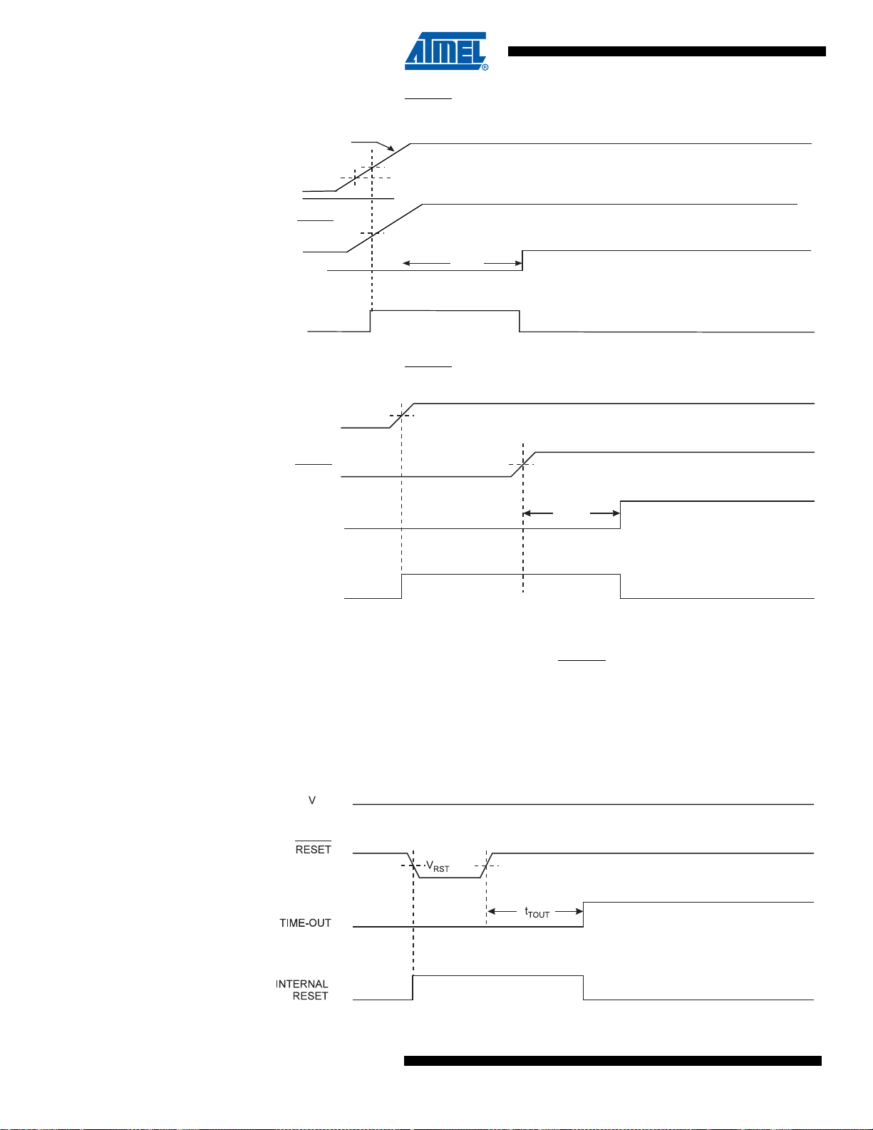
ATmega16/32/64/M1/C1
Figure 7-2. MCU Start-up, RESET Tied to V
T
I
V
V
CCRR
CC
V
PORMAX
V
PORMIN
CC
RESET
TIME-OUT
INTERNAL
RESET
V
RST
t
TOUT
Figure 7-3. MCU Start-up, RESET Extended Externally
V
V
CC
RESET
IME-OUT
NTERNAL
RESET
POT
V
RST
t
TOUT
7.2.2 External Reset
An External Reset is ge nerated by a low level on the RESET
pin. Reset pulses longer than the
minimum pulse width (see Table 7-1) will generate a reset, even i f the clock is not running.
Shorter pulse s are not gu arante ed to gene rate a reset . When the applie d signal rea ches the
Reset Threshold Voltage – V
the Time-out period – t
TOUT –
– on its positive edge, the delay counter starts the MCU after
RST
has expired.
Figure 7-4. External Reset During Operation
CC
48
7647D–AVR–08/08
Page 49

7.2.3 Brown-out Detection
ATmega16/32/64/M1/C1 has an On-chip Brown-out Detection (BOD) circuit for monitoring the
V
level during op eration by comp aring it to a fixed tri gger l evel. The trigger level fo r the BOD
CC
can be selected by the BODLEV EL Fuses. The trigg er level has a hyster esis to ensure spik e
free Brown-out Detection. The hysteresis on the detection level should be interpreted as V
V
BOT
Table 7-2. BODLEVEL Fuse Coding
+ V
HYST
/2 and V
BOT-
= V
BOT
- V
HYST
/2.
(1)(2)
ATmega16/32/64/M1/C1
=
BOT+
BODLEVEL 2..0 Fuses Min V
BOT
Typ V
BOT
Max V
BOT
Units
111 2.6
110
RESERVED101
100
011 4.3 V
010 2.7 V
001 4.5 V
000 DISABLED
Notes: 1. V
may be below nominal minimum operating voltage for some devices. For devices where
BOT
this is the case, the device is tested down to V
antees that a Brown-Out Reset will occur before V
CC
= V
during the production test. This guar-
BOT
drops to a voltage where correct
CC
operation of the microcontroller is no longer guaranteed. The test is performed using
BODLEVEL = 010 for Low Operating Voltage and BODLEVEL = 101 for High Operating Voltage .
2. Valu es are guidel in es onl y.
Table 7-3. Brown-out Characterist ic s
(1)
Symbol Parameter Min. Typ. Max. Units
V
t
BOD
HYST
Brown-out Detector Hysteresis 50 mV
Min Pulse Width on Brown-out Reset 2 µs
7647D–AVR–08/08
Notes: 1. V alu es are guidel in es only.
When the BOD is enabled, and VCC decreases to a value below the trigger level (V
7-5), the Brown-ou t R es et i s im mediately activated. W he n V
(V
in Figure 7-5), the delay counter s tarts the MCU afte r the Time-out period t
BOT+
increases abov e th e t rigge r le ve l
CC
expired.
The BOD circuit will onl y dete ct a dr op in V
ger than t
given in Table 7-3.
BOD
if the voltage stays bel ow the tr igger leve l for lon-
CC
in Figure
BOT-
TOUT
has
49
Page 50

ATmega16/32/64/M1/C1
Figure 7-5. Brown-out Reset During Operation
T
I
7.2.4 Watchdog Reset
V
CC
RESET
IME-OUT
NTERNAL
RESET
V
BOT-
V
BOT+
t
TOUT
When the Watchdog times out, i t will gen erate a short r eset pul se of one CK cycle duration . On
the falling edge of this pul se, the delay timer starts co unting the Time-out pe riod t
TOUT
. Refer to
page 52 for details on operation of the Watchdog Timer.
Figure 7-6. Watchdog Reset During Operation
CC
7.2.5 MCU Status Register – MCUSR
The MCU Status Register provides information on which reset source caused an MCU reset.
Bit 76543210
Read/Write R R R R R/W R/W R/W R/W
Initial Value 0000 See Bit Description
• Bit 3 – WDRF: Watchdog Reset Flag
This bit is set if a W atchdog Re se t occurs. The bit i s reset by a P ower-on Reset, or by wr iting a
logic zero to the flag.
• Bit 2 – BORF: Brown-out Reset Flag
This bit is set if a Brown-out Reset occurs. The bit is reset by a Power-on Reset, or by writing a
logic zero to the flag.
• Bit 1 – EXTRF: External Reset Flag
CK
– – – – WDRF BORF EXTRF PORF MCUSR
50
7647D–AVR–08/08
Page 51

This bit is set if an Exte rnal Rese t occurs. Th e bit is res et by a Powe r-on Res et, or by writi ng a
logic zero to the flag.
• Bit 0 – PORF: Power-on Reset Flag
This bit is set if a Power-on Reset occurs. The bit is reset only by writing a logic zero to the flag.
To make use of the Reset flags to identify a reset condition, the user should read and then reset
the MCUSR as early as possible in the program. If the register is cleared befor e another reset
occurs, the source of the reset can be found by examining the reset flags.
7.3 Internal Voltage Reference
ATmega16/32/64/M1/C1 features an internal bandgap reference. This reference is used for
Brown-out DetectionDetection, and it can be used as an input to the Analog Comparators or the
ADC. The V
internal bandgap reference.
7.3.1 Voltage Reference Enable Signals and Start-up Time
The voltage reference has a start-up time that may influence the way it should be used. The
start-up time is given in Table 7-4. To save power, the reference is not always turned on. The
reference is on during the following situations:
1. When the BOD is enabled (by programming the BODLEVEL [2..0] Fuse).
2. When the bandgap reference is connected to the Analog Comparator (by setting the
ACBG bit in ACSR).
3. When the ADC is enabled.
4. When the DAC is enabled.
2.56V reference to the ADC, DAC or Analog Comparators is generated from the
REF
ATmega16/32/64/M1/C1
Thus, when the BOD is not enabled, after setting the ACBG bit or enabling the ADC or the DAC,
the user must always allo w the refer enc e to start u p bef or e the outp ut from th e An al og Co mpa rator or ADC or DAC is used. To red uce power c onsumpti on in Po wer-down m ode, the us er can
avoid the three conditions above to ensure that the reference is turned off before entering
Power-down mode.
7.3.2 Voltage Reference Characteristics
Table 7-4. Internal Voltage Reference Characteristics
Symbol Parameter Condition Min. Typ. Max. Units
V
BG
t
BG
I
BG
Note: 1. Values are guidelines only.
Bandgap reference voltage 1.1 V
Bandgap reference start-up time 40 µs
Bandgap reference current
consumption
(1)
15 µA
7647D–AVR–08/08
51
Page 52

ATmega16/32/64/M1/C1
7.4 Watchdog Timer
ATmega16/32/64/M1/C1 has an Enhanced Watchdog Timer (WDT). The main features are:
•
• 3 Operating modes
• Selectable Time-out period from 16ms to 8s
• Possible Hardware fuse Watchdog always on (WDTON) for fail-safe mode
Figure 7-7. Watchdog Timer
Clocked from separate On-chip Oscillator
– Interrupt
– System Reset
– Interrupt and System Reset
128 KHz
OSCILLATOR
WDP3
WDIF
OSC/2K
OSC/8K
OSC/4K
MCU RESET
WDIE
INTERRUPT
The Watchdog Tim er ( WDT) i s a ti me r co unti ng cy cles o f a se par ate on -chi p 1 28 kHz o sc illa tor .
The WDT gives an interrupt or a system reset when the counter reaches a given time-out value.
In normal operation mode, it is required that the system uses the WDR - Watchdog Timer Reset
- instruction to res tart the counte r before th e time-out va lue is reac hed. If the syst em doesn't
restart the counter, an interrupt or system reset will be issued.
In Interrupt mode, the WDT gives an interrupt when the timer expires. This interrupt can be used
to wake the device from sleep-modes, and also as a general system timer. One example is to
limit the maximum time allowed for certain operati ons, giving an interr upt when the operatio n
has run longer than expected. I n System Res et mode, the WDT giv es a rese t when the ti mer
expires. Thi s is t ypica lly used t o prev ent sy stem hang- up in case o f run away c ode. The t hird
mode, Interrupt and System Res et mod e, co mb ine s the other two mo des by firs t givi ng an inte rrupt and then switch to System Reset mode. Th is mode wil l for inst ance allow a sa fe shutdow n
by saving critical parameters before a system reset.
The “Watchdog Timer Always On” (WDTON) fuse, if programmed, will force the Watchdog Timer
to System Reset mode. With the fuse programmed the System Reset mode bit (WDE) and Interrupt mode bit (WDIE) are locked to 1 and 0 respectively . To further ensure program secur ity,
alterations to the Watchdog set-up must follow timed sequences. The sequence for clearing
WDE and changing time-out configuration is as follows:
1. In the same operation, write a logic one to the Watchdog change enable bit (WDCE) and
WDE. A logic one must be written to WDE r egardle ss of th e previous value of the WDE
bit.
2. Within the next four clock cycle s, write the WDE and Watchdog prescale r bits (WDP) as
desired, but with the WDCE bit cleared. This must be done in one operation.
52
7647D–AVR–08/08
Page 53

ATmega16/32/64/M1/C1
The following cod e exa mple sh ows on e ass embly and on e C fun ction for turning off the Watc hdog Timer. The example assumes that interrupts are controlled (e.g. by dis abling interrupts
globally) so that no interrupts will occur during the execution of these functions.
Assembly Code Example
WDT_off:
; Turn off global interrupt
cli
; Reset Watchdog Timer
wdr
; Clear WDRF in MCUSR
in r16, MCUSR
andi r16, (0xff & (0<<WDRF))
out MCUSR, r16
; Write logical one to WDCE and WDE
; Keep old prescaler setting to prevent unintentional time-out
lds r16, WDTCSR
ori r16, (1<<WDCE) | (1<<WDE)
sts WDTCSR, r16
; Turn off WDT
ldi r16, (0<<WDE)
sts WDTCSR, r16
; Turn on global interrupt
sei
ret
C Code Example
(1)
(1)
void WDT_off(void)
{
__disable_interrupt();
__watchdog_reset();
/* Clear WDRF in MCUSR */
MCUSR &= ~(1<<WDRF);
/* Write logical one to WDCE and WDE */
/* Keep old prescaler setting to prevent unintentional time-out */
WDTCSR |= (1<<WDCE) | (1<<WDE);
/* Turn off WDT */
WDTCSR = 0x00;
__enable_interrupt();
}
Note: 1. The example code assumes that the part specific header file is included.
Note: If the Watchdog is accidentally enabled, for example by a runaway pointer or brown-out
condition, the device will be reset and the Watchdog Timer will stay enabled. If the code is not
set up to handle the Watchdog, this might lead to an eternal loop of time-out resets. To avoid this
situation, the app lication soft ware should alwa ys clear the W atchdog System Reset Flag
(WDRF) and the WDE control bit in the initialisation routine, even if the Watchdog is not in use.
7647D–AVR–08/08
53
Page 54

ATmega16/32/64/M1/C1
The following code example shows one a ssembl y and one C fu nction fo r ch anging the ti me-out
value of the Watchdog Timer.
Assembly Code Example
WDT_Prescaler_Change:
; Turn off global interrupt
cli
; Reset Watchdog Timer
wdr
; Start timed sequence
lds r16, WDTCSR
ori r16, (1<<WDCE) | (1<<WDE)
sts WDTCSR, r16
; -- Got four cycles to set the new values from here -
; Set new prescaler(time-out) value = 64K cycles (~0.5 s)
ldi r16, (1<<WDE) | (1<<WDP2) | (1<<WDP0)
sts WDTCSR, r16
; -- Finished setting new values, used 2 cycles -
; Turn on global interrupt
sei
ret
C Code Example
(1)
(1)
void WDT_Prescaler_Change(void)
{
__disable_interrupt();
__watchdog_reset();
/* Start timed equence */
WDTCSR |= (1<<WDCE) | (1<<WDE);
/* Set new prescaler(time-out) value = 64K cycles (~0.5 s) */
WDTCSR = (1<<WDE) | (1<<WDP2) | (1<<WDP0);
__enable_interrupt();
}
Note: 1. The example code assumes that the part specific header file is included.
Note: The Watchdog Timer sh oul d be reset b efo re any ch ange of the WDP bi ts, si nce a ch ang e
in the WDP bits can result in a time-out when switching to a shorter time-out period;
7.4.1 Watchdog Timer Control Register - WDTCSR
Bit 76543210
WDIF WDIE WDP3 WDCE WDE WDP2 WDP1 WDP0 WDTCSR
Read/Write R/W R/W R/W R/W R/W R/W R/W R/W
Initial Value 0 0 0 0 X 0 0 0
• Bit 7 - WDIF: Watchdog Interrupt Flag
This bit is set when a time-out occurs in the Wat chdog T im er and the Watc hd og Time r is confi gured for interrupt. WDIF is cleared by hardware when executing the corresponding interrupt
handling vector. Alternatively, WDIF is cleared by writing a logic one to the flag. When the I-bit in
SREG and WDIE are set, the Watchdog Time-out Interrupt is executed.
54
7647D–AVR–08/08
Page 55

ATmega16/32/64/M1/C1
• Bit 6 - WDIE: Watchdog Interrupt Enable
When this bit is written to one and the I-bit in the Status Register is set, the Watchdog Interrupt is
enabled. If WDE is cleared in combination with this setting, the Watchdog Timer is in Interrupt
Mode, and the corresponding interrupt is executed if time-out in the Watchdog Timer occurs.
If WDE is set, t he W atch dog Time r is in Interrup t and Syst em Re set Mode. The first time-o ut i n
the Watchdog Timer will set WDIF . Execu ting the corresponding interrupt vec to r wil l clear WDIE
and WDIF automatic ally by hardware (the Watc hdog go es to S ystem Res et Mode ). This is us eful for keeping the Watchdo g Timer secu rity while usin g the interrupt. To s tay in Interrupt a nd
System Reset Mode, WDIE must be set after each interrupt. This should however not be done
within the interrupt service routine itself, as this might compromise the safety-function of the
Watchdog System Re set mode . If the inte rrupt is not e xecuted be fore the nex t time-ou t, a System Reset will be applied.
Table 7-5. Watchdog Timer Configuration
WDTON
(1)
0 0 0 Stopped None
0 0 1 Interrupt Mode Interrupt
0 1 0 System Reset Mode Reset
WDE WDIE Mode Action on Time-out
011
1 x x System Reset Mode Reset
Note: 1. For the WDTON Fuse “1” means unprogrammed while “0” means programmed.
Interrupt and System Reset
Mode
Interrupt, then go to System
Reset Mode
• Bit 4 - WDCE: Watchdog Change Enable
This bit is used in timed seq uen ce s for changing WDE and prescale r bi ts. T o cl ea r th e WDE bi t,
and/or change the prescaler bits, WDCE must be set.
Once written to one, hardware will clear WDCE after four clock cycles.
• Bit 3 - WDE: Watchdog System Reset Enable
WDE is overridden by WDRF in MCUSR. This means that WDE i s always set when WDRF is
set. To clear WDE, WDRF must be cleared first. This feature ensures multiple resets during conditions causing failure, and a safe start-up after the failure.
• Bit 5, 2..0 - WDP3..0: Watchdog Timer Prescaler 3, 2, 1 and 0
The WDP3..0 bi ts deter mine th e Watc hdog Ti mer pre scalin g when th e Watc hdog Ti mer is ru nning. The different prescaling values and their corresponding time-out periods are shown in
Table 7-6 on page 56.
7647D–AVR–08/08
55
Page 56

ATmega16/32/64/M1/C1
.
Table 7-6. Watchdog Timer Prescale Select
Number of WDT Oscillator
WDP3 WDP2 WDP1 WDP0
0 0 0 0 2K (2048) cycles 16 ms
0 0 0 1 4K (4096) cycles 32 ms
0 0 1 0 8K (8192) cycles 64 ms
0 0 1 1 16K (16384) cycles 0.125 s
0 1 0 0 32K (32768) cycles 0.25 s
0 1 0 1 64K (65536) cycles 0.5 s
0 1 1 0 128K (131072) cycles 1.0 s
0 1 1 1 256K (262144) cycles 2.0 s
1 0 0 0 512K (524288) cycles 4.0 s
1 0 0 1 1024K (1048576) cycles 8.0 s
1010
1011
1100
1101
1110
1111
Cycles
Reserved
T ypi cal T im e-o ut at
VCC = 5.0V
56
7647D–AVR–08/08
Page 57

8. Interrupts
This section describ es the specifics of the interrupt handling as performed in
ATmega16/32/64/M1/C1. For a general explanation of the AVR interrupt handling, refer to
“Reset and Interrupt Handling” on page 18.
8.1 Interrupt Vectors in ATmega16/32/64/M1/C1
Table 8-1. Reset and Interrupt Vectors
ATmega16/32/64/M1/C1
Vector
No.
1 0x0000 RESET
2 0x0002 ANACOMP 0 Analog Comparator 0
3 0x0004 ANACOMP 1 Analog Comparator 1
4 0x0006 ANACOMP 2 Analog Comparator 2
5 0x0008 ANACOMP 3 Analog Comparator 3
6 0x000A PSC FAULT
7 0x000C PSC EC
8 0x000E INT0 External Interrupt Request 0
9 0x0010 INT1 External Interrupt Request 1
10 0x0012 INT2 External Interrupt Request 2
11 0x0014 INT3 External Interrupt Request 3
12 0x0016 TIMER1 CAPT Timer/Counter1 Capture Event
13 0x0018 TIMER1 COMPA Timer/Counter1 Compare Match A
14 0x001A TIMER1 COMPB Timer/Counter1 Compare Match B
15 0x001C TIMER1 OVF Timer/Counter1 Overflow
16 0x001E TIMER0 COMPA Timer/Counter0 Compare Match A
Program
Address Source Interrupt Definition
External Pin, Power-on Reset, Brown-out Reset,
Watchdog Reset, and Emulation AVR Reset
(3)
(3)
PSC Fault
PSC End of Cycle
7647D–AVR–08/08
17 0x0020 TIMER0 COMPB Timer/Counter0 Compare Match B
18 0x0022 TIMER0 OVF Timer/Counter0 Overflow
19 0x0024 CAN INT CAN MOB, Burst, General Errors
20 0x0026 CAN TOVF CAN Timer Overflow
21 0x0028 LIN TC LIN Transfer Complete
22 0x002A LIN ERR LIN Error
23 0x002C PCINT0 Pin Change Interrupt Reques t 0
24 0x002E PCINT1 Pin Ch an ge Inter rupt R equ es t 1
25 0x0030 PCINT2 Pin Change Interrupt Request 2
26 0x0032 PCINT3 Pin Change Interrupt Request 3
27 0x0034 SPI, STC SPI Serial Transfer Complete
28 0x0036 ADC ADC Conversion Complete
57
Page 58

ATmega16/32/64/M1/C1
Table 8-1. Reset and Interrupt Vectors
Vector
No.
29 0x0038 WDT Watchdog Time-Out Interrupt
30 0x003A EE READY EEPROM Ready
31 0x003C SPM R EADY Store Program Memory Ready
Notes: 1. When the BOOTRST Fuse is programmed, the device will jump to the Boot Loader address at
Program
Address Source Interrupt Definition
reset, see “Boot Loader Support – Read-While-Write Self-Programming
ATmega16/32/64/M1/C1” on page 276.
2. When the IVSEL bit in MCUCR is set, Interrupt Ve ctors will be moved to the start of the Boot
Flash Section. The address of each Interrupt Vector will then be the address in this table
added to the start address of the Boot Flash Section.
3. These vectors are not used by ATmega32/64C1.
Table 8-2 shows reset and Interrupt Vectors placement for the various combinations of
BOOTRST and IVSEL settings. If the program never enables an interrupt source, the Interrupt
Vectors are not used, and regular program code can be placed at these locations. This is also
the case if the Reset Vector is in the Application s ection while the Interrupt V ectors are in the
Boot section or vice versa.
Table 8-2. Reset and Interrupt Vectors Placement in ATmega16/32/64/M1/C1
BOOTRST IVSEL Reset Address Interrupt Vectors Start Address
1 0 0x000 0x001
(1)
1 1 0x000 Boot Reset Address + 0x002
0 0 Boot Reset Address 0x001
0 1 Boot Reset Address Boot Reset Address + 0x002
Note: 1. The Boot Reset Address is shown in Table 24-4 on page 281. For the BOOTRST Fuse “1”
means unprogrammed while “0” means programmed.
The most typical and general program setup for the Reset and Interrupt Vector Addresses in
ATmega16/32/64/M1/C1 is:
Address Labels Code Comments
0x000 jmp RESET ; Reset Handler
0x002 jmp ANA_COMP_0 ; Analog Comparator 0 Handler
0x004 jmp ANA_COMP_1 ; Analog Comparator 1 Handler
0x006 jmp ANA_COMP_2 ; Analog Comparator 2 Handler
0x008 jmp ANA_COMP_3 ; Analog Comparator 3 Handler
0x00A jmp PSC_FAULT ; PSC Fault Handler
0x00C jmp PSC_EC ; PSC End of Cycle Handler
0x00E jmp EXT_INT0 ; IRQ0 Handler
0x010 jmp EXT_INT1 ; IRQ1 Handler
0x012 jmp EXT_INT2 ; IRQ2 Handler
0x014 jmp EXT_INT3 ; IRQ3 Handler
0x016 jmp TIM1_CAPT ; Timer1 Capture Handler
0x018 jmp TIM1_COMPA ; Timer1 Compare A Handler
0x01A jmp TIM1_COMPB ; Timer1 Compare B Handler
0x01C jmp TIM1_OVF ; Timer1 Overflow Handler
58
7647D–AVR–08/08
Page 59

ATmega16/32/64/M1/C1
0x01E jmp TIM0_COMPA ; Timer0 Compare A Handler
0x020 jmp TIM0_COMPB ; Timer0 Compare B Handler
0x022 jmp TIM0_OVF ; Timer0 Overflow Handler
0x024 jmp CAN_INT ; CAN MOB,Burst,General Errors Handler
0x026 jmp CAN_TOVF ; CAN Timer Overflow Handler
0x028 jmp LIN_TC ; LIN Transfer Complete Handler
0x02A jmp LIN_ERR ; LIN Error Handler
0x02C jmp PCINT0 ; Pin Change Int Request 0 Handler
0x02E jmp PCINT1 ; Pin Change Int Request 1 Handler
0x030 jmp PCINT2 ; Pin Change Int Request 2 Handler
0x032 jmp PCINT3 ; Pin Change Int Request 3 Handler
0x034 jmp SPI_STC ; SPI Transfer Complete Handler
0x036 jmp ADC ; ADC Conversion Complete Handler
0x038 jmp WDT ; Watchdog Timer Handler
0x03A jmp EE_RDY ; EEPROM Ready Handler
0x03C jmp SPM_RDY ; Store Program Memory Ready Handler
;
0x03ERESET: ldi r16, high(RAMEND); Main program start
0x03F out SPH,r16 ; Set Stack Pointer to top of RAM
0x040 ldi r16, low(RAMEND)
0x041 out SPL,r16
0x042 sei ; Enable interrupts
0x043 <instr> xxx
... ... ... ...
When the BOOTRST Fuse is unprogrammed, the Boot section size set to 2K bytes and the
IVSEL bit in the MCUCR Regis ter is set before a ny interru pts are enabl ed, the m ost typica l and
general program setup for the Reset and Interrupt Vector Addresses in ATmega16/32/64/M1/C1
is:
Address Labels Code Comments
0x000 RESET: ldi r16,high(RAMEND); Main program start
0x001 out SPH,r16 ; Set Stack Pointer to top of RAM
0x002 ldi r16,low(RAMEND)
0x003 out SPL,r16
0x004 sei ; Enable interrupts
0x005 <instr> xxx
;
.org 0xC02
0xC02 jmp ANA_COMP_0 ; Analog Comparator 0 Handler
0xC04 jmp ANA_COMP_1 ; Analog Comparator 1 Handler
... ... ... ;
0xC3C jmp SPM_RDY ; Store Program Memory Ready Handler
When the BOOTRST Fuse is programmed and the Boot section size set to 2K bytes, the most
typical and general program setup for the Reset and I nterrupt Vector Addresses in
ATmega16/32/64/M1/C1 is:
Address Labels Code Comments
.org 0x002
0x002 jmp ANA_COMP_0 ; Analog Comparator 0 Handler
7647D–AVR–08/08
59
Page 60

ATmega16/32/64/M1/C1
0x004 jmp ANA_COMP_1 ; Analog Comparator 1 Handler
... ... ... ;
0x03C jmp SPM_RDY ; Store Program Memory Ready Handler
;
.org 0xC00
0xC00 RESET: ldi r16,high(RAMEND); Main program start
0xC01 out SPH,r16 ; Set Stack Pointer to top of RAM
0xC02 ldi r16,low(RAMEND)
0xC03 out SPL,r16
0xC04 sei ; Enable interrupts
0xC05 <instr> xxx
When the BOOTRST Fuse is prog ra mme d, the Boot sect io n si ze set to 2K byte s an d the IV SE L
bit in the MCUCR Register is set before any interrupts are enabled, the most typical and general
program setup for the Reset and Interrupt Vector Addresses in ATmega16/32/64/M1/C116/32 is:
Address Labels Code Comments
;
.org 0xC00
0xC00 jmp RESET ; Reset handler
0xC02 jmp ANA_COMP_0 ; Analog Comparator 0 Handler
0xC04 jmp ANA_COMP_1 ; Analog Comparator 1 Handler
... ... ... ;
0xC3C jmp SPM_RDY ; Store Program Memory Ready Handler
;
0xC3E RESET: ldi r16,high(RAMEND); Main program start
0xC3F out SPH,r16 ; Set Stack Pointer to top of RAM
0xC40 ldi r16,low(RAMEND)
0xC41 out SPL,r16
0xC42 sei ; Enable interrupts
0xC43 <instr> xxx
8.1.1 Moving Interrupts Between Application and Boot Space
The MCU Control Register controls the placement of the Interrupt Vector table.
8.1.2 MCU Control Register – MCUCR
Bit 76543210
Read/Write R/W R R R/W R R R/W R/W
Initial Value00000000
• Bit 1 – IVSEL: Interrupt Vector Select
When the IVSEL bit is cleared (zero), the Interrupt Vectors are placed at the start of the Flash
memory. When this bit is set (one), the Interrupt Vectors are moved to the beginning of the Boot
Loader section of the Flash. The actual address of the start of the Boot Flash Section is determined by the BOOTSZ Fuses. Refer to the section “Boot Loader Support – Read-While-Write
Self-Programming ATmega16/32/64/M1/C1” on page 276 for details. To avoid unintentional
60
SPIPS – – PUD – – IVSEL IVCE MCUCR
7647D–AVR–08/08
Page 61

ATmega16/32/64/M1/C1
changes of Interru pt Vecto r table s, a spec ial writ e procedu re must be follow ed to cha nge the
IVSEL bit:
1. Write the Interrupt Vector Change Enable (IVCE) bit to one.
2. Within four cycles, write the desired value to IVSEL while writing a zero to IVCE.
Interrupts will automa tic al ly be di sa bled while this sequence is exe cu ted. In ter r upts ar e di sa ble d
in the cycle IVCE is set, an d they remain disabled until aft er the i nst ruct ion following the write to
IVSEL. If IVSEL is not written, interrupts remain disabled for four cycles. The I-bit in the Status
Register is unaffected by the automatic disa bling.
Note: If Interrupt Vectors are placed in the Boot Loader section and Boot Lock bit BLB02 is pro-
grammed, interrupts are disabled while executing from the Application section. If Interrupt Vectors
are placed in the Application section and Boot Lock bit BLB12 is programed, interrupts are disabled while executing from the Boot Loader section. Refer to the section “Boot Loader Support –
Read-While-Write Self-Programming ATmega16/32/64/M1/C1” on page 276 for details on Boot
Lock bits.
• Bit 0 – IVCE: Interrupt Vector Change Enable
The IVCE bit must be written to logic one to ena ble c hang e o f the IV SE L b it. IVC E i s cl ear e d by
hardware four cycles af ter i t i s writte n o r whe n IV S EL is wr itten . S etti ng the IV CE bi t will di s able
interrupts, as explained in the IVSEL description above. See Code Example below.
Assembly Code Example
Move_interrupts:
; Enable change of Interrupt Vectors
ldi r16, (1<<IVCE)
out MCUCR, r16
; Move interrupts to Boot Flash section
ldi r16, (1<<IVSEL)
out MCUCR, r16
ret
C Code Example
void Move_interrupts(void)
{
/* Enable change of Interrupt Vectors */
MCUCR = (1<<IVCE);
/* Move interrupts to Boot Flash section */
MCUCR = (1<<IVSEL);
}
7647D–AVR–08/08
61
Page 62

ATmega16/32/64/M1/C1
9. I/O-Ports
r
9.1 Introduction
All AVR ports have true R ead-Modify -Write fu nctional ity when used as general digi tal I/O ports .
This means that the direction of one port pin can be c hanged without unintentionally changing
the direction of any other pin with th e SBI an d CBI i nstruc tions . The s ame app lies when cha nging drive value (if configured as output) or enabling/disabling of pull-up resistors (if configured as
input). Each output buffer has symmetrical drive characteristics with both high sink and source
capability. All port pins have individually selectable pull-up resistors with a supply-voltage invariant resistance. All I/O pins have protection diodes to both V
and Ground as indicated in Figure
CC
9-1. Refer to “Electrical Characteristics” on page 315 for a complete list of parameters.
Figure 9-1. I/O Pin Equivalent Schematic
R
pu
Pxn
C
pin
"General Digital I/O" fo
Logic
See Figure
Details
All registers and bit references in this section are written in general form. A lower case “x” represents the numbering letter for the port, and a lower case “n” represents the bit number. However,
when using the register or bit defines in a program, the precise form must be used. For example,
PORTB3 for bit no. 3 in Port B, here documented generally as PORTxn. The physical I/O Registers and bit locations are listed in “Register Description for I/O-Ports”.
Three I/O memory address locations are allocated for each port, one each for the Data Register
– PORTx, Data Directi on Regi ster – D DRx, and the Por t Input P ins – P INx. The Port Input Pins
I/O location is read only, while the Data Re gister and the Data Direc tio n Regi st er are rea d/writ e.
However, writing a logic one to a bit in the PINx Register, will result in a toggle in the corresponding bit in the Data Register. In addition, the Pull-up Disable – PUD bit in MCUCR disables the
pull-up function for all pins in all ports when set.
Using the I/O port as Gen eral D igital I/O is des c ribed in “ Po rts as G ene ral Di gi tal I/ O”. M o st port
pins are multiplexed with alternate functions for the peripheral features on the device. How each
alternate function interferes with the port pin is described in “Alte rnate Po rt Func tion s” o n pa ge
67. Refer to the individual module sections for a full description of the alternate functions.
Note that enabling the alternate function of some of the port pins does not affect the use of the
other pins in the port as general digital I/O.
62
7647D–AVR–08/08
Page 63

9.2 Ports as General Digital I/O
The ports are bi-directi onal I/O ports with optional inter nal pull-ups . Figure 9-2 show s a functional description of one I/O-port pin, here generically called Pxn.
ATmega16/32/64/M1/C1
Figure 9-2. General Digital I/O
Pxn
(1)
SLEEP
SYNCHRONIZER
DLQ
D
PINxn
Q
PUD
Q
D
DDxn
Q
CLR
RESET
D
Q
PORTxn
Q
CLR
RESET
Q
Q
RRx
WDx
RDx
RPx
clk
1
0
WPx
WRx
I/O
DATA B U S
Note: 1. WRx, WPx, WDx, RRx, RPx, and RDx are common to all pins within the same port. clk
9.2.1 Configuring the Pin
Each port pin con sis ts o f three regi ster bits: DDxn, P ORTx n, and PINx n. As shown in “Register
Description for I/O-Ports” on page 81, the DDxn bi ts are acces sed at the DDRx I/O address, the
PORTxn bits at the PORTx I/O address, and the PINxn bits at the PINx I/O address.
The DDxn bit in the DDRx Re gister selects th e direction of t his pin. If DDxn i s written logi c on e,
Pxn is configured as an output pin. If DDxn is written logic zero, Pxn is configured as an input
pin.
If PORTxn is writt en logi c one when the pin is c onfigur ed as an input pin, th e pull- up resi stor is
activated. To switch the pull-up resistor off, PORTxn has to be written logic zero or the pin has to
be configured as an output pin
The port pins are tri-stated when reset condition becomes active, even if no clocks are running.
PUD: PULLUP DISABLE
SLEEP: SLEEP CONTROL
clk
: I/O CLOCK
I/O
SLEEP, and PUD are common to all ports.
WDx: WRITE DDRx
RDx: READ DDRx
WRx: WRITE PORTx
RRx: READ PORTx REGISTER
RPx: READ PORTx PIN
WPx: WRITE PINx REGISTER
I/O
,
7647D–AVR–08/08
63
Page 64

ATmega16/32/64/M1/C1
If PORTxn is writ ten lo gic one when the pin is confi gu re d a s an output pin, the port pi n is d ri ven
high (one). If PORTxn is wr itten logic zero when the pin is configured as an output pi n, the port
pin is driven low (zero).
9.2.2 Toggling the Pin
Writing a logic one to P INx n t oggl es the value of PORTxn, in dep end ent on the value of DDRxn.
Note that the SBI instruction can be used to toggle one single bit in a port.
9.2.3 Switching Between Input and Output
When switching betwe en t ri- sta te ( {DDx n, P ORT xn} = 0b0 0) an d ou tput hi gh ({DD xn, PO RTx n}
= 0b11), an intermediate state with either pull- up enabled {DDxn, P ORTxn} = 0b01) or output
low ({DDxn, PORTxn} = 0b10) must occur. Normally, the pull-up enabled state is fully acceptable, as a high-impedant en vi ronme nt wi ll not noti ce the di ffer en ce betwee n a strong high driver
and a pull-up. If this is not the case, the PUD bit in the MCUCR Register can be set to disable all
pull-ups in all ports.
Switching between input with pull-up and output low generates the same problem. The user
must use either the tri-state ({DDxn, PORTxn} = 0b00) or the output high state ({DDxn, PORTxn}
= 0b11) as an intermediate step.
Table 9-1 summarizes the control signals for the pin value.
Table 9-1. Port Pin Configurations
DDxn PORTxn
PUD
(in MCUCR) I/O Pull-up Comment
0 0 X Input No
0 1 0 Input Yes Pxn will source current if ext. pulled low.
0 1 1 Input No Tri -state (Hi-Z)
1 0 X Output No Output Low (Sink)
1 1 X Output No Output High (Source)
9.2.4 Reading the Pin Value
Independent of the setting of Data Direction bit DDxn, the port pin can be r ead through the
PINxn Register bit. As shown in Figure 9-2, the PINxn Regist er bit and the precedi ng latch c onstitute a synchr onizer. T his is needed to avoid metastabi lity if th e physi cal pin change s value
near the edge of the internal clock, but it also introduces a delay. Figure 9-3 shows a timing diagram of the synchronization when reading a n externally applied pin value. The maximum and
minimum propagation delays are denoted t
pd,max
and t
Default configuration after Reset.
Tri-state (Hi-Z)
respectively.
pd,min
64
7647D–AVR–08/08
Page 65
ATmega16/32/64/M1/C1
Figure 9-3. Synchronization when Reading an Externally Applied Pin value
SYSTEM CLK
INSTRUCTIONS
XXX in r17, PINx
XXX
SYNC LATCH
PINxn
r17
0x00 0xFF
t
pd, max
t
pd, min
Consider the clock period starting shortly after the first falling edge of the system clock. The latch
is closed when the clock is low, and goes transparent when the clock is high, as indicated by the
shaded region of the “S YNC LATCH” signal. The s ignal v alue is l atche d when t he syste m clock
goes low. It is clocked into the PINxn Register a t the succeeding pos itive clock edge. A s indicated by the two arr ows t
pd,max
and t
, a single signal transition on the pin will be delayed
pd,min
between ½ and 1½ system clock period depending upon the time of assertion.
When reading back a software assigned pin value, a nop in struction must be inserted as indi-
cated in Figure 9-4. The out instruction sets the “SYNC LATCH” signal at the positive edge of
the clock. In this case, the delay t
through the synchronizer is 1 system clock period.
pd
Figure 9-4. Synchronization when Reading a Software Assigned Pin Value
7647D–AVR–08/08
SYSTEM CLK
r16
INSTRUCTIONS
out PORTx, r16 nop in r17, PINx
0xFF
SYNC LATCH
PINxn
r17
0x00 0xFF
t
pd
The following code e xampl e s ho ws how to set port B pins 0 and 1 hi gh, 2 an d 3 lo w, an d de fin e
the port pins from 4 to 7 as input with pull-ups assigned to port pins 6 and 7. The resulting pin
65
Page 66

ATmega16/32/64/M1/C1
values are read back again, but as previously discussed, a nop instruction is included to be able
to read back the value recently assigned to some of the pins.
Assembly Code Example
...
; Define pull-ups and set outputs high
; Define directions for port pins
ldi r16, (1<<PB7)|(1<<PB6)|(1<<PB1)|(1<<PB0)
ldi r17, (1<<DDB3)|(1<<DDB2)|(1<<DDB1)|(1<<DDB0)
out PORTB, r16
out DDRB, r17
; Insert nop for synchronization
nop
; Read port pins
in r16, PINB
...
(1)
C Code Example
unsigned char i;
...
/* Define pull-ups and set outputs high */
/* Define directions for port pins */
PORTB = (1<<PB7)|(1<<PB6)|(1<<PB1)|(1<<PB0);
DDRB = (1<<DDB3)|(1<<DDB2)|(1<<DDB1)|(1<<DDB0);
/* Insert nop for synchronization*/
_NOP();
/* Read port pins */
i = PINB;
...
Note: 1. For the assembly program, two temporary registers are used to minimize the time from pull-
ups are set on pins 0, 1, 6, and 7, until the direction bits are correctly set, defining bit 2 and 3
as low and redefining bits 0 and 1 as strong high drivers.
9.2.5 Digital Input Enable and Sleep Modes
As shown in Figure 9-2, the digital input signal can be clamped to ground at the input of the
schmitt-trigger. The signal denoted SLEEP in the figure, is set by the MCU Sleep Controller in
Power-down mode, Power-save mode, and Standby mode to avoid high power consumption if
some input signals are left floating, or have an analog signal level close to V
SLEEP is overridden for port pins enabled as external interrupt pins. If the external interrupt
request is not enabled, SLEEP is active also for these pins. SLEEP is also overridden by various
other alternate functions as described in “Alternate Port Functions” on page 67.
If a logic high level (“one”) is present on an Asynchronous External Interrupt pin configured as
“Interrupt on Rising Edge, Falling Edge, or Any Logic Change on Pin” while the external interrupt
is not enabled, th e corresp onding Ex ternal Int errupt Fl ag will be se t when resu ming from th e
above mentioned sleep modes, as the clamping in these sleep modes produces the requested
logic change.
66
CC
/2.
7647D–AVR–08/08
Page 67

9.3 Alternate Port Functions
PTOExn: Pxn, PORT TOGGLE OVERRIDE ENABLE
Most port pins have alternate functions in addition to being general digital I/Os. Figure 9-5 shows
how the port pin c ontrol signals fr om the s implifie d Figur e 9-2 can be overr idden by al ternate
functions. The overriding signals may not be present in all port pins, but the f igure serv es as a
generic description applicable to all port pins in the AVR microcontroller family.
ATmega16/32/64/M1/C1
Figure 9-5. Alternate Port Functions
1
0
1
0
Pxn
1
0
1
0
(1)
PUOExn
PUOVxn
DDOExn
DDOVxn
PVOExn
PVOVxn
DIEOExn
DIEOVxn
SLEEP
SYNCHRONIZER
SET
DLQ
D
PINxn
Q
CLR
PUD
D
Q
DDxn
Q
CLR
RESET
Q
D
PORTxn
Q
CLR
RESET
Q
Q
CLR
1
0
WDx
RDx
RRx
clk
RPx
PTOExn
WPx
WRx
I/O
DATA BUS
7647D–AVR–08/08
DIxn
AIOxn
PUOExn: Pxn PULL-UP OVERRIDE ENABLE
PUOVxn: Pxn PULL-UP OVERRIDE VALUE
DDOExn: Pxn DATA DIRECTION OVERRIDE ENABLE
DDOVxn: Pxn DATA DIRECTION OVERRIDE VALUE
PVOExn: Pxn PORT VALUE OVERRIDE ENABLE
PVOVxn: Pxn PORT VALUE OVERRIDE VALUE
DIEOExn: Pxn DIGITAL INPUT-ENABLE OVERRIDE ENABLE
DIEOVxn: Pxn DIGITAL INPUT-ENABLE OVERRIDE VALUE
SLEEP: SLEEP CONTROL
Note: 1. WRx, WPx, WDx, RRx, RPx, and RDx are common to all pins within the same port. clk
PUD: PULLUP DISABLE
WDx: WRITE DDRx
RDx: READ DDRx
RRx: READ PORTx REGISTER
WRx: WRITE PORTx
RPx: READ PORTx PIN
WPx: WRITE PINx
: I/O CLOCK
clk
I/O
DIxn: DIGITAL INPUT PIN n ON PORTx
AIOxn: ANALOG INPUT/OUTPUT PIN n ON PORTx
I/O
SLEEP, and PUD are common to all ports. All other signals are unique for each pin.
Table 9-2 summariz es the function of the over riding signa ls. The pi n and po rt indexe s from Figure 9-5 are not shown in the suc cee ding tables . Th e over ridin g si gnals are gener ated inte rnally
in the modules having the alternate function.
67
,
Page 68

ATmega16/32/64/M1/C1
Table 9-2. Generic Description of Overriding Signals for Alternate Functions
Signal Name Full Name Description
If this signal is set, th e pull-up enable is cont rolled by the PU OV
signal. If this signal is cleared, the pull-up is enabled when
{DDxn, PORTxn, PUD} = 0b010.
If PUOE is set, the pull-up is enabled/disabled when PUOV is
set/cleared, regardless of the setting of the DDxn, PORTxn,
and PUD Register bits.
If this signal is s et, the Ou tput Driv er Enable i s controlled by the
DDOV signal. If this signal is cleared, the Output driver is
enabled by the DDxn Register bit.
If DDOE is set, the Output Driver is enabled/disabled when
DDOV is set/cleared, regardless of the setting of the DDxn
Register bit.
If this signal is set and the Output Driver is enabled, the port
value is controll ed by the PVOV s ignal . If PVO E is cl eared, and
the Output Driver is enabl ed, the port Value is controlled by the
PORTxn Register bit.
PUOE
PUOV
DDOE
DDOV
PVOE
Pull-up Over ride
Enable
Pull-up Over ride
Value
Data Direction
Override Enable
Data Direction
Override Value
Port Value
Override Enable
PVOV
PTOE
DIEOE
DIEOV
DI Digital Input
AIO
Port Value
Override Value
Port Toggle
Override Enable
Digital Input
Enable Override
Enable
Digital Input
Enable Override
Value
Analog
Input/Output
If PVOE is set, the port value is set to PVOV, regardless of the
setting of the PORTxn Register bit.
If PTOE is set, the PORTxn Register bit is inverted.
If this bit is set, the Digital Input Enable is controlled by the
DIEOV signal. If this signal is cleared, the Digital Input Enable
is determined by MCU state (Normal mode, sleep mode).
If DIEOE is set, the Digital Input is enabled/disabled when
DIEOV is set/cleared, regardless of the MCU state (Normal
mode, sleep mode).
This is the Digital Input to alternate functions. In the figure, the
signal is connected to the output of the schmitt trigger but
before the synchronizer. Unless the Digital Inpu t is used as a
clock source, the module with the alternate function will use its
own synchronizer.
This is the Analog Input/o utp ut to/from alternate functions. The
signal is connected directly to the pad, and can be used bidirectionally.
The following subsections shortly describe the alternate functions for each port, and relate the
overriding signals to the alternat e function. Refer to the alternate func tion descripti on for further
details.
68
7647D–AVR–08/08
Page 69

9.3.1 MCU Control Register – MCUCR
Bit 7 6 5 4 3 2 1 0
SPIPS – –PUD– – IVSEL IVCE MCUCR
Read/Write R/W R R R/W R R R/W R/W
Initial Value 0 0 0 0 0 0 0 0
• Bit 4 – PUD: Pull-up Disable
When this bit is written to one, the pull-ups in the I/O ports ar e disabled even if the DDxn and
PORTxn Registers are configured to enable the pull-ups ({DDxn, PORTxn} = 0b01). Se
9.3.2 Alternate Functions of Port B
The Port B pins with alternate functions are shown in Table 9-3.
Table 9-3. Port B Pins Alternate Functions
Port Pin Alternate Functions
PSCOUT0B (PSC output 0B)
PB7
ADC4 (Analog Input Channel 4)
SCK (SPI Bus Serial Clock)
PCINT7 (Pin Change Interrupt 7)
ATmega16/32/64/M1/C1
PB6
PB5
PB4
PB3
PB2
PB1
PB0
ADC7 (Analog Input Channel 7)
PSCOUT1B (PSC output 1B)
PCINT6 (Pin Change Interrupt 6)
ADC6 (Analog Input Channel 6)
INT2 (External Interrupt 2)
ACMPN1 (Analog Comparator 1 Negative Input)
AMP2- (Analog Differential Amplicator 2 Negative Input)
PCINT5 (Pin Change Interrupt 5)
AMP0+ (Analog Diffe rential Amplifier 0 Positive Input)
PCINT4 (Pin Change Interrupt 4)
AMP0- (Analog Differential Amplifier 0 Negative Input)
PCINT3 (Pin Change Interrupt 3)
ADC5 (Analog Input Channel5 )
INT1 (External Interrupt 1)
ACMPN0 (Analog Comparator 0 Negative Input)
PCINT2 (Pin Change Interrupt 2)
MOSI (SPI Master Out Slave In)
PSCOUT2B (PSC output 2B)
PCINT1 (Pin Change Interrupt 1)
MISO (SPI Master In Slave Out)
PSCOUT2A (PSC output 2A)
PCINT0 (Pin Change Interrupt 0)
7647D–AVR–08/08
The alternate pin configuration is as follows:
• ADC4/PSCOUT0B/SCK/PCINT7 – Bit 7
PSCOUT0B, Output 0B of PSC.
69
Page 70

ATmega16/32/64/M1/C1
ADC4, Analog to Digital Converter, input channel 4.
SCK, Master Clock output, S lav e Clo ck inp ut pi n for SPI chan nel . Whe n the SP I is enab led as a
slave, this pin is configured as an inpu t regardless of the setting of DDB7. When the SPI is
enabled as a master, the data dir ection of this pin is controlled by DDB7. When the pin is force d
to be an input, the pull-up can still be controlled by the PORTB7 bit.
PCINT7, Pin Change Interrupt 7.
• ADC7/PSCOUT1B/PCINT6 – Bit 6
ADC7, Analog to Digital Converter, input channel 7
PSCOUT1B, Output 1B of PSC.
PCINT6, Pin Change Interrupt 6.
• ADC6/INT2
ADC6, Analog to Digital Converter, input channel 6
INT2, External Interrupt source 2. This pin can serve as an External Interrupt source to the MCU.
ACMPN1, Analog Compa rator 1 Ne gati ve Inp ut. Co nfi gur e th e po rt pin as inp ut wi th th e in ter na l
pull-up switched off to avoid the digital port function from interfering with the function of the Analog Comparator.
PCINT5, Pin Change Interrupt 5.
• APM0+/PCINT4 – Bit 4
AMP0+, Analog Differential Amplifier 0 Positive Input Channel.
PCINT4, Pin Change Interrupt 4.
• AMP0-/PCINT3 – Bit 3
AMP0-, Analog Differential Amplifier 0 Negative Input Channel. Configure the port pin as input
with the internal pull-up sw itched off to avoi d the digital port functi on from interferin g with the
function of the Analog Amplifier.
PCINT3, Pin Change Interrupt 3.
• ADC5/INT1
/ACMPN1/AMP2-/PCINT5 – Bit 5
/ACMPN0/PCINT2 – B it 2
.
.
70
ADC5, Analog to Digital Converter, input channel 5
INT1, External Interrupt source 1. This pin can serve as an external interrupt source to the MCU.
ACMPN0, Analog Compa rator 0 Ne gati ve Inp ut. Co nfi gur e th e po rt pin as input with the internal
pull-up switched off to avoid the digital port function from interfering with the function of the Analog Comparator.
PCINT2, Pin Change Interrupt 2.
• PCINT1/MOSI/PSCOUT2B – Bit 1
MOSI: SPI Master Data output, Slave Data input for SPI channel. When the SPI is enabled as a
slave, this pi n is config ured as an input re gardless of the setting of DDB1 When the SPI is
enabled as a master, the data dir ection of this pin is controlled by DDB1. When the pin is force d
to be an input, the pull-up can still be controlled by the PORTB1 and PUD bits.
PSCOUT2B, Output 2B of PSC.
PCINT1, Pin Change Interrupt 1.
• PCINT0/MISO/PSCOUT2A – Bit 0
.
7647D–AVR–08/08
Page 71
ATmega16/32/64/M1/C1
MISO, Master Data input , Slave Dat a output p in for S PI channe l. When the SPI is ena bled as a
master, this pin is co nfigured as an inpu t regardles s of the settin g of DDB0. When the SP I is
enabled as a slave, the data direction of this pin is controlled by DDB0. When the pin is forced to
be an input, the pull-up can still be controlled by the PORTB0 and PUD bits.
PSCOUT2A, Output 2A of PSC.
PCINT0, Pin Change Interrupt 0.
Table 9-4 and Table 9-5 rel ates the al ter nat e func tions of Por t B to the ove rri din g si gna ls sho wn
in Figure 9-5 on page 67.
Table 9-4. Overriding Signals for Alternate Functions in PB7. .PB4
PB7/ADC4/
PSCOUT0B/SCK/
Signal Name
PUOE SPE • MSTR
PUOV PB7 • PUD • SPIPS 000
DDOE
DDOV PSCen01 1 0 0
PVOE SPE • MSTR • SPIPS
PVOV
DIEOE ADC4D ADC7D ADC6D + In2en AMP0ND
DIEOV 0 0 In2en 0
DI
AIO ADC4 ADC7 ADC6 AMP0+
PCINT7
• SPIPS 000
SPE • MSTR
+ PSCen01
PSCout01 • SPIPS +
PSCout01 •
PSCen01 • SPIPS
+ PSCout01 •
PSCen01 • SPIPS
SCKin • SPIPS
ireset
• SPIPS
•
PB6/ADC7/
PSCOUT1B/
PCINT6
PSCen11 0 0
PSCen11 0 0
PSCOUT11 0 0
ICP1B INT2
PB5/ADC6/
INT2/ACMPN1/
AMP2-/PCINT5
PB4/AMP0+/
PCINT4
7647D–AVR–08/08
71
Page 72

ATmega16/32/64/M1/C1
Table 9-5. Overriding Signals for Alternate Functions in PB3. .PB0
PB1/MOSI/
PB3/AMP0-/
Signal Name
PUOE00––
PUOV00––
DDOE00––
DDOV00––
PVOE00––
PVOV00––
DIEOE AMP0ND ADC5D + In1en 0 0
DIEOV 0 In1en 0 0
DI INT1
AIO AMP0- ADC5 – –
PCINT3
PB2/ADC5/INT1/
ACMPN0/PCINT2
PSCOUT2B/
PCINT1
MOSI_IN • SPIPS
• ireset
PB0/MISO/
PSCOUT2A/
PCINT0
MISO_IN • SPIPS
• ireset
72
7647D–AVR–08/08
Page 73

9.3.3 Alternate Functions of Port C
The Port C pins with alternate functions are shown in Table 9-6.
Table 9-6. Port C Pins Alternate Functions
Port Pin Alternate Function
PC7
PC6
PC5
PC4
ATmega16/32/64/M1/C1
D2A (DAC output )
AMP2+ (Analog Differential Amplifier 2 Positive Input)
PCINT15 (Pin Change Interrupt 15)
ADC10 (Analog Input Channel 10)
ACMP1 (Analog Comparator 1 Positive Input )
PCINT14 (Pin Change Interrupt 14)
ADC9 (Analog Input Channel 9)
AMP1+ (Analog Differential Amplifier 1 Input Channel )
ACMP3 (Analog Comparator 3 Positive Input )
PCINT13 (Pin Change Interrupt 13)
ADC8 (Analog Input Channel 8)
AMP1- (Analog Differential Amplifier 1 Input Channel )
ACMPN3 (Analog Comparator 3 Negative Input)
PCINT12 (Pin Change Interrupt 12)
T1 (Timer 1 clock input)
PC3
PC2
PC1
PC0
Note: On the engineering samp les (Parts marked AT90PWM324), th e ACMP N3 altern ate func tion i s not
located on PC4. It is located on PE2.
RXCAN (CAN Rx Data)
ICP1B (Timer 1 input capture alternate input)
PCINT11 (Pin Change Interrupt 11)
T0 (Timer 0 clock input)
TXCAN (CAN Tx Data)
PCINT10 (Pin Change Interrupt 10)
PSCIN1 (PSC 1 Digital Input)
OC1B (Timer 1 Output Compare B)
SS_A (Alternate SPI Slave Select)
PCINT9 (Pin Change Interrupt 9)
PSCOUT1A (PSC output 2A)
INT3 (External Interrupt 3)
PCINT8 (Pin Change Interrupt 8)
The alternate pin configuration is as follows:
• D2A/AMP2+/PCINT15 – Bit 7
D2A, Digital to Analog output
AMP2+, Analog Differential Amp lifier 2 Po sitive Input. Con figure the port pin as input with the
internal pull-up switc hed off to avoid the digital port fun ction from int erfering wit h the functio n of
the Amplifier.
7647D–AVR–08/08
PCINT15, Pin Change Interrupt 15.
• ADC10/ACMP1/PCINT14 – Bit 6
ADC10, Analog to Digital Converter, input channel 10.
73
Page 74

ATmega16/32/64/M1/C1
ACMP1, Analog Comparator 1 Positive Inp ut. Configure the port pin as input with the internal
pull-up switched off to avoid the digital port function from interfering with the function of the Analog Comparator.
PCINT14, Pin Change Interrupt 14.
• ADC9/ACMP3/AMP1+/PCINT13 – Bit 5
ADC9, Analog to Digital Converter, input channel 9.
ACMP3, Analog Comparator 3 Positive Inp ut. Configure the port pin as input with the internal
pull-up switched off to avoid the digital port function from interfering with the function of the Analog Comparator.
AMP1+, Analog Differential Amplifier 1 Positive Input Channel. Configure the port pin as input
with the internal pull-up sw itched off to avoi d the digital port functi on from interferin g with the
function of the Analog Amplifier.
PCINT13, Pin Change Interrupt 13.
• ADC8/AMP1-/ACMPN3/PCINT12 – Bit 4
ADC8, Analog to Digital Converter, input channel 8.
AMP1-, Analog Differential Amplifier 1 Negative Input Channel. Configure the port pin as input
with the internal pull-up sw itched off to avoi d the digital port functi on from interferin g with the
function of the Analog Amplifier.
ACMPN3, Analog Compa rator 3 Ne gati ve Inp ut. Co nfi gur e th e po rt pin as input with the internal
pull-up switched off to avoid the digital port function from interfering with the function of the Analog Comparator.
PCINT12, Pin Change Interrupt 12.
• PCINT11/T1/RXCAN/ICP1B – Bit 3
T1, Timer/Counter1 counter source.
RXCAN, CAN Rx Data.
ICP1B, Input Capture Pin: The PC3 pin can act as an Input Capture Pin for Timer/Counter1.
PCINT11, Pin Change Interrupt 11.
• PCINT10/T0/TXCAN – Bit 2
T0, Timer/Counter0 counter source.
TXCAN, CAN Tx Data.
PCINT10, Pin Change Interrupt 10.
• PCINT9/PSCIN1/OC1B/SS_A – Bit 1
PCSIN1, PSC 1 Digital Input.
OC1B, Output Compare Match B output: This pin can serve as an external output for the
Timer/Counter1 Output Compare B. The pin has to be configured as an output (DDC1 set “one”)
to serve this function. This pin is also the output pin for the PWM mode timer function.
SS
_A: Slave Port Select in put. Whe n the SPI is enabled as a sla ve, this pi n is confi gured as an
input regardle ss of the setting of DD D0. As a sl ave, th e SPI is ac tivated wh en this pi n is drive n
low. When the SPI is enabl ed as a ma ster, the data di rection of this pin i s contro lled by DDD0.
When the pin is forced to be an input, the pull-up can still be controlled by the PORTD0 bit.
PCINT9, Pin Change Interrupt 9.
• PCINT8/PSCOUT1A/INT3
74
– Bit 0
7647D–AVR–08/08
Page 75
ATmega16/32/64/M1/C1
PSCOUT1A, Output 1A of PSC.
INT3, External Interrupt source 3: This pin can serve as an external interrupt source to the MCU.
PCINT8, Pin Change Interrupt 8.
Table 9-7 and Table 9-8 relate the alternate func tions of Por t C to the overridin g signal s shown
in Figure 9-5 on page 67.
Table 9-7. Overriding Signals for Alternate Functions in PC7..PC4
PC6/ADC10/
PC7/D2A/AMP2+/
Signal Name
PUOE 0 0 0
PUOV 0 0 0
DDOE DAEN 0 0 0
DDOV 0 0 0 0
PVOE 0 0 0 –
PVOV 0 0 0 –
DIEOE DAEN ADC10D ADC9D ADC8D
DIEOV 0 0 0 0
DI
AIO – ADC10 Amp1 ADC9 Amp1+
PCINT15
ACMP1/
PCINT14
PC5/ADC9/
AMP1+/ACMP3/
PCINT13
PC4/ADC8/
AMP1-
/ACMPN3/
PCINT12
ADC8 Amp1ACMPN3
Table 9-8. Overriding Signals for Alternate Functions in PC3..PC0
Signal Name
PC3/T1/RXCAN/
ICP1B/PCINT11
PC2/T0/TXCAN/
PCINT10
PC1/PSCIN1/
OC1B/SS_A/
PCINT9
PC0/INT3/
PSCOUT1A/
PCINT8
7647D–AVR–08/08
PUOE0000
PUOV0000
DDOE 0 PSCen10
DDOV1101
PVOE OC1Ben PSCen10
PVOV OC1B PSCout10
DIEOE In3en
DIEOV In3en
DI T1 T0
AIO
PSCin1
SS_A
INT3
75
Page 76

ATmega16/32/64/M1/C1
9.3.4 Alternate Functions of Port D
The Port D pins with alternate functions are shown in Table 9-9.
Table 9-9. Port D Pins Alternate Functions
Port Pin Alternate Function
PD7
PD6
PD5
PD4
PD3
PD2
ACMP0 (Analog Comparator 0 Positive Input )
PCINT23 (Pin Change Interrupt 23)
ADC3 (Analog Input Channel 3 )
ACMPN2 (Analog Compara tor 2 Negati ve Inpu t)
INT0 (External Interrupt 0)
PCINT22 (Pin Change Interrupt 22)
ADC2 (Analog Input Channel 2)
ACMP2 (Analog Comparator 2 Positive Input )
PCINT21 (Pin Change Interrupt 21)
ADC1 (Analog Input Channel 1)
RXD/RXLIN (LIN/UART Rx data)
ICP1A (Timer 1 input capture)
SCK_A (Programming & alternate SPI Clock)
PCINT20 (Pin Change Interrupt 20)
TXD/TXLIN (LIN/UART Tx data)
OC0A (Timer 0 Output Compare A)
SS (SPI Slave Select)
MOSI_A (Programming & alternate SPI Master Out Slave In)
PCINT19 (Pin Change Interrupt 19)
PSCIN2 (PSC Digital Input 2)
OC1A (Timer 1 Output Compare A)
MISO_A (Programming & alternate Master In SPI Slave Out)
PCINT18 (Pin Change Interrupt 18)
76
PSCIN0 (PSC Digital Input 0)
PD1
PD0
CLKO (System Clock Output)
PCINT17 (Pin Change Interrupt 17)
PSCOUT0A (PSC output 0A)
PCINT16 (Pin Change Interrupt 16)
The alternate pin configuration is as follows:
• ACMP0/PCINT23 – Bit 7
ACMP0, Analog Comparator 0 Positive Inp ut. Configure the port pin as input with the internal
pull-up switched off to avoid the digital port function from interfering with the function of the Analog Comparator.
PCINT23, Pin Change Interrupt 23.
• ADC3/ACMPN2/INT0
/PCINT22 – Bit 6
ADC3, Analog to Digital Converter, input channel 3.
7647D–AVR–08/08
Page 77

ATmega16/32/64/M1/C1
ACMPN2, Analog Compa rator 2 Ne gati ve Inp ut. Co nfi gur e th e po rt pin as input with the internal
pull-up switched off to avoid the digital port function from interfering with the function of the Analog Comparator.
INT0, External Interrupt source 0. This pin can serve as an external interrupt source to the MCU.
PCINT22, Pin Change Interrupt 23.
• ADC2/ACMP2/PCINT21 – Bit 5
ADC2, Analog to Digital Converter, input channel 2.
ACMP2, Analog Comparator 1 Positive Inp ut. Configure the port pin as input with the internal
pull-up switched off to avoid the digital port function from interfering with the function of the Analog Comparator.
PCINT21, Pin Change Interrupt 21.
• PCINT20/ADC1/RXD/RXLIN/ICP1/SCK_A – Bit 4
ADC1, Analog to Digital Converter, input channel 1.
RXD/RXLIN, LIN/UART Receive Pin. Receive Data (Data input pin for the LIN/UART). When the
LIN/UART receiver is enabled this pin is configured as an input regardless of the value of
DDRD4. When the UART forces this pin to be an input, a logical one in PORTD4 will turn on the
internal pull-up.
ICP1, Input Capture Pin1: This pin can act as an input capture pin for Timer/Counter1.
SCK_A: Master Clock output, Slave Clock input pin for SPI channel. When the SPI is enabled as
a slave, this pin is c onfigured as an input regardles s of the setti ng of DDD4. W hen the SPI is
enabled as a master, the data direction of this pin is controlled by DDD4. When the pin is forced
to be an input, the pull-up can still be controlled by the PORTD4 bit.
PCINT20, Pin Change Interrupt 20.
• PCINT19/TXD/TXLIN/OC0A/SS/MOSI_A, Bit 3
TXD/TXLIN, LIN/UART Transmit pin. Data output pin for the LIN /UART. When the LIN/UART
Transmitter is enabled, this pin is configured as an output regardless of the value of DDD3.
OC0A, Output Compare Match A output: This pin can serve as an external output for the
Timer/Counter0 Output Compare A. The pin has to be configured as an output (DDD3 set “one”)
to serve this function. The OC0A pin is also the output pin for the PWM mode
SS
: Slave Port Sel ect input . When the SPI is e nabled as a slave, this pin i s configur ed as an
input regardle ss of the se tting of DD D3. As a sl ave, th e SPI is ac tivated wh en this pi n is drive n
low. When the SPI is enabl ed as a ma ster, the data di rection of this pin i s contro lled by DDD3.
When the pin is forced to be an input, the pull-up can still be controlled by the PORTD3 bit.
MOSI_A: SPI Master Data output, Slave Data input for SPI channel. When the SPI is enabled as
a slave, this pin is configured as an input regardless of the setting of DDD3 When the SPI is
enabled as a master, the data direction of this pin is controlled by DDD3. When the pin is forced
to be an input, the pull-up can still be controlled by the PORTD3 bit.
PCINT19, Pin Change Interrupt 19.
• PCINT18/PSCIN2/OC1A/MISO_A, Bit 2
7647D–AVR–08/08
PCSIN2, PSC Digital Input 2.
OC1A, Output Compare Match A output: This pin can serve as an external output for the
Timer/Counter1 Output Compare A. The pin has to be configured as an output (DDD2 set “one”)
to serve this function. The OC1A pin is also the output pin for the PWM mode timer function.
77
Page 78

ATmega16/32/64/M1/C1
MISO_A: Master Data input, Slave Data output pin for SPI channel. When the SPI is enabled as
a master, this pin is configured as an input regardless of the setting of DDD2. When the SPI is
enabled as a slave, the data direction of this pin is controlled by DDD2. When the pin is forced to
be an input, the pull-up can still be controlled by the PORTD2 bit.
PCINT18, Pin Change Interrupt 18.
• PCINT17/PSCIN0/CLKO – Bit 1
PCSIN0, PSC Digital Input 0.
CLKO, Divided System Clock: The divided system clock can be output on this pin. The divided
system clock will be ou tput if th e CKOUT Fuse is progra mmed, re gardle ss of the POR TD1 and
DDD1 settings. It will also be output during reset.
PCINT17, Pin Change Interrupt 17.
• PCINT16/PSCOUT0A – Bit 0
PSCOUT0A: Output 0 of PSC 0.
PCINT16, Pin Change Interrupt 16.
Table 9-10 and Table 9-11 relates the alternate functions of Port D to the overriding signals
shown in Figure 9-5 on page 67.
Table 9-10. Overriding Signals for Alternate Functi ons PD7..PD4
PD7/
ACMP0/
Signal Name
PUOE 0 0 0
PUOV 0 0 0
DDOE 0 0 0
DDOV 0 0 0 0
PVOE 0 0 0
PVOV 0 0 0 –
DIEOE ACMP0D ADC3D + In0en ADC2D ADC1D
DIEOV 0 In0en 0 0
DI – INT0 ICP1A
AIO ACOMP0
PCINT23
PD6/ADC3/
ACMPN2/INT0/
PCINT22
ADC3
ACMPM
PD5/ADC2/
ACMP2/PCINT21
ADC2
ACOMP2
PD4/ADC1/RXD/
RXLIN/ICP1A/
SCK_A/PCINT20
RXEN + SPE •
MSTR
PD4 •
PUD
RXEN + SPE •
MSTR
SPE • MSTR •
SPIPS
ADC1
• SPIPS
• SPIPS
78
7647D–AVR–08/08
Page 79

ATmega16/32/64/M1/C1
Table 9-11. Overriding Signals for Alternate Functions in PD3..PD0
PD3/TXD/TXLIN/
OC0A/SS/MOSI_A/
Signal Name
PUOE
PUOV
DDOE
DDOV TXEN 0 0 PSCen00
PVOE
PVOV
DIEOE 0 0 0 0
DIEOV 0 0 0 0
DI
PCINT19
TXEN + SPE •
MSTR
• SPIPS
TXEN • SPE • MS TR
• SPIPS
TXEN + SPE •
MSTR • SPIPS
TXEN + OC0en +
SPE •
MSTR • SPIPS
TXEN • TXD + TXEN
• (OC0en • OC0 +
OC0en • SPIPS •
MOSI)
SS
MOSI_Ain
• PD3 • PUD
PD2/PSCIN2/
OC1A/MISO_A/
PCINT18
–0
– 0 PD0 • PUD
–0
– 0 PSCen00 + UMSEL
–0–
PD1/PSCIN0/
CLKO/
PCINT17
PD0/PSCOUT0A/
XCK/PCINT16
SPE •
MSTR • SPIPS
PSCen00 + SPE •
MSTR • SPIPS
AIO
9.3.5 Alternate Functions of Port E
The Port E pins with alternate functions are shown in Table 9-12.
Table 9-12. Port E Pins Alternate Functions
Port Pin Alternate Function
XTAL2 (XTAL Output)
PE2
PE1
PE0
Note: On the engineering samp les (Parts marked AT90PWM324), th e ACMP N3 altern ate func tion i s not
ADC0 (Analog Input Channel 0)
PCINT26 (Pin Change Interrupt 26)
XTAL1 (XTAL Input)
OC0B (Timer 0 Output Compare B)
PCINT25 (Pin Change Interrupt 25)
RESET# (Reset Input)
OCD (On Chip Debug I/O)
PCINT24 (Pin Change Interrupt 24)
located on PC4. It is located on PE2.
7647D–AVR–08/08
79
Page 80

ATmega16/32/64/M1/C1
The alternate pin configuration is as follows:
• PCINT26/XTAL2/ADC0 – Bit 2
XTAL2: Chip clock Oscillator pin 2. Used as clock pin for crystal Oscillator or Low-frequency
crystal Oscillator. When used as a clock pin, the pin can not be used as an I/O pin.
ADC0, Analog to Digital Converter, input channel 0.
PCINT26, Pin Change Interrupt 26.
• PCINT25/XTAL1/OC0B – Bit 1
XTAL1: Chip clock Oscillator pin 1. Used for all chip clock sources except internal calibrated RC
Oscillator. When used as a clock pin, the pin can not be used as an I/O pin.
OC0B, Output Compare Match B output: This pin can serve as an external output for the
Timer/Counter0 Output Compare B. The pin has to be configured as an output (DDE1 set “one”)
to serve this function. This pin is also the output pin for the PWM mode timer function.
PCINT25, Pin Change Interrupt 25.
• PCINT24/RESET
/OCD – Bit 0
RESET
, Reset pin: When the RSTDISBL Fuse is programmed, this pin functions as a normal I/O
pin, and the part will have to rely on Power -on Reset an d Brown-o ut Reset as its reset sou rces.
When the RSTDISBL Fuse is unprogrammed, the reset circuitry is connected to the pin, and the
pin can not be used as an I/O pin.
If PE0 is used as a reset pin, DDE0, PORTE0 and PINE0 will all read 0.
PCINT24, Pin Change Interrupt 24.
Table 9-13 relates the alter na te func ti ons of Port E to the ove rri din g si gna ls sho wn in Figure 9-5
on page 67.
Table 9-13. Overriding Signals for Alternate Functions in PE2..PE0
PE2/ADC0/XTAL2/
Signal Name
PUOE 0 0 0
PUOV 0 0 0
DDOE 0 0 0
DDOV 0 0 0
PVOE 0 OC0Ben 0
PVOV 0 OC0B 0
DIEOE ADC0D 0 0
PCINT26
PE1/XTAL1/OC0B/
PCINT25
PE0/RESET
OCD/PCINT24
/
DIEOV 0 0 0
DI
AIO
80
Osc Output
ADC0
Osc / Clock input
7647D–AVR–08/08
Page 81
9.4 Register Description for I/O-Ports
9.4.1 Port B Data Register – PORTB
Bit 76543210
PORTB7 PORTB6 PORTB5 PORTB4 PORTB3 PORTB2 PORTB1 PORTB0 PORTB
Read/Write R/W R/W R/W R/W R/W R/W R/W R/W
Initial Value00000000
9.4.2 Port B Data Direction Register – DDRB
Bit 76543210
DDB7 DDB6 DDB5 DDB4 DDB3 DDB2 DDB1 DDB0 DDRB
Read/Write R/W R/W R/W R/W R/W R/W R/W R/W
Initial Value00000000
9.4.3 Port B Input Pins Address – PINB
Bit 76543210
PINB7 PINB6 PINB5 PINB4 PINB3 PINB2 PINB1 PINB0 PINB
Read/Write R/W R/W R/W R/W R/W R/W R/W R/W
Initial Value N/A N/A N/A N/A N/ A N/A N/A N/A
ATmega16/32/64/M1/C1
9.4.4 Port C Data Register – PORTC
Bit 76543210
PORTC7 PORTC6 PORTC5 PORTC4 PORTC3 PORTC2 PORTC1 PORTC0 PORTC
Read/Write R/W R/W R/W R/W R/W R/W R/W R/W
Initial Value00000000
9.4.5 Port C Data Direction Register – DDRC
Bit 76543210
DDC7 DDC6 DDC5 DDC4 DDC3 DDC2 DDC1 DDC0 DDRC
Read/Write R/W R/W R/W R/W R/W R/W R/W R/W
Initial Value00000000
9.4.6 Port C Input Pins Address – PINC
Bit 76543210
PINC7 PINC6 PINC5 PINC4 PINC3 PINC2 PINC1 PINC0 PINC
Read/Write R/W R/W R/W R/W R/W R/W R/W R/W
Initial Value N/A N/A N/A N/A N/ A N/A N/A N/A
9.4.7 Port D Data Register – PORTD
Bit 76543210
PORTD7 PORTD6 PORTD5 PORTD4 PORTD3 PORTD2 PORTD1 PORTD0 PORTD
Read/Write R/W R/W R/W R/W R/W R/W R/W R/W
Initial Value00000000
9.4.8 Port D Data Direction Register – DDRD
Bit 76543210
DDD7 DDD6 DDD5 DDD4 DDD3 DDD2 DDD1 DDD0 DDRD
Read/Write R/W R/W R/W R/W R/W R/W R/W R/W
Initial Value00000000
7647D–AVR–08/08
81
Page 82

ATmega16/32/64/M1/C1
9.4.9 Port D Input Pins Address – PIND
Bit 76543210
PIND7 PIND6 PIND5 PIND4 PIND3 PIND2 PIND1 PIND0 PIND
Read/Write R/W R/W R/W R/W R/W R/W R/W R/W
Initial Value N/A N/A N/A N/A N/ A N/A N/A N/A
9.4.10 Port E Data Register – PORTE
Bit 76543210
– – – – – PORTE2 PORTE1 PORTE0 PORTE
Read/Write R R R R R R/W R/W R/W
Initial Value00000000
9.4.11 Port E Data Direction Register – DDRE
Bit 76543210
– – – – – DDE2 DDE1 DDE0 DDRE
Read/Write R R R R R R/W R/W R/W
Initial Value00000000
9.4.12 Port E Input Pins Address – PINE
Bit 76543210
– – – – – PINE2 PINE1 PINE0 PINE
Read/Write R R R R R R/W R/W R/W
Initial Value 0 0 0 0 0 N/A N/A N/A
82
7647D–AVR–08/08
Page 83

10. External Interrupts
The External Interrupts are triggered by the INT3:0 pins or any of the PCINT23..0 pins. Observe
that, if enabled, the interrupts will trigger even if the INT3:0 or PCINT23..0 pins are configured as
outputs. This feature provides a way of generating a software interrupt. The pin change interrupt
PCI2 will trigger if any enabled PCINT23..16 pin toggles. The pi n ch ang e inte rrup t PCI1 will trigger if any enabled PCINT14..8 pin toggles. The pin change inte rrupt PCI0 will trigge r if any
enabled PCINT7..0 pin toggles. The PCMSK3, PCMSK2, PCMSK1 and PCMSK0 Registers
control which p ins co ntri bute t o the pin chan ge in terr upts. Pin cha nge inte rrup ts o n PCIN T26.. 0
are detected asynchr onous ly. Th is im plies t hat thes e int errupts can be us ed for wak ing t he part
also from sleep modes other than Idle mode.
The INT3:0 interrupts can be trig ger ed by a fall in g or risin g edge or a low le ve l. T his is set up as
indicated in the specification for the External Interr upt Control Regis ter A – EICRA. When the
INT3:0 interrupts are e nabled and are co nfigur ed as level tr iggered, the inte rrupts w ill trig ger as
long as the pin is held low. Note that recognition of falling or rising edge interrupts on INT3:0
requires the presence of an I/O clock, described in “Clock Systems and their Distribution” on
page 30. Low level interrupt on INT3:0 is detected asynchronously. This implies that this inter-
rupt can be used for waking the part al so fro m sl eep mod es other tha n Idl e mo de. T he I/O clo ck
is halted in all sleep modes except Idle mode.
Note that if a level triggered interrupt is used for wake-up from Power-down, the required level
must be held long enough for the MCU to complete the wake-up to trigger the level interrupt. If
the level disappears before the end of the Start-up Time, the MCU will still wake up, but no interrupt will be generated. T he sta rt-up time i s defi ned by the S UT an d CKSE L Fuses as desc ribed
in “Clock Systems and their Distribution” on page 30.
ATmega16/32/64/M1/C1
10.1 Pin Change Interrupt Timing
An example of timing of a pin change interrupt is schown in Figure 10-1.
Figure 10-1. Timing of a pin change interrupts
PCINT[i]
pin
clk
DQ
LE
clk
PCINT[i] pin
pin_lat
pin_sync
pcint_in[i]
pcint_syn
pcint_set/flag
pin_lat pin_sync pcint_in[i]
DQ
PCINT[i] bit
(of PCMSK
)
n
0
7
clk
pcint_sync pcint_set/flag
DQ DQ DQ
PCIF
n
(interrupt
flag)
7647D–AVR–08/08
PCIF
n
83
Page 84

ATmega16/32/64/M1/C1
10.2 External Interrupt Control Register A – EICRA
The External Interrupt Control Register A contains control bits for interrupt sense control.
Bit 76543210
ISC31 ISC30 ISC21 ISC20 ISC11 ISC10 ISC01 ISC00 EICRA
Read/Write R/W R/W R/W R/W R/W R/W R/W R/W
Initial Value00000000
• Bit 7..0 – ISC31, ISC30 - ISC01, ISC00: Interrupt Sense Control 0 Bit 1 and Bit 0
The External Interrupts 3 - 0 are activated by the external pins INT3:0 if the SREG I-flag and the
corresponding interru pt ma sk in t he E IMS K i s set. T he lev el and edges on the external pins th at
activate the interrupt are defined in Table 10-1. Edges on INT3..INT0 are registered asynchronously. The value on the INT3:0 pins are sampled before detecting edges. If edge or toggle
interrupt is selected, pulses that last longer than one clock period will generate an interrupt.
Shorter pulses are not gua rante ed to gene rate an interr upt. Obse rve that C PU clock freque ncy
can be lower than XTAL frequency if the XTAL divider is enabled. If low level interrup t is
selected, the low level must be held until the completion of the currently executing instruction to
generate an interrupt. If en abled, a level trig gered int erru pt will gen erate a n inter rupt req uest as
long as the pin is held low.
Table 10-1. Interrupt Sense Control
ISCn1 ISCn0 Description
0 0 The low level of INTn generates an interrupt request.
0 1 Any logical change on INTn generates an interrupt request.
1 0 The fallin g e dg e between two samples of INTn generate s an interrupt request.
1 1 The rising edge between two samples of INTn generates an interrupt request.
Note: 1. n = 3, 2, 1 or 0.
When changing the ISCn1/ISCn0 bits, the interrupt must be disabled by clearing its Interrupt
Enable bit in the EIMSK Regist er. Otherwise an interrupt can occur when the bit s are c hanged .
10.2.1 External Interrupt Mask Register – EIMSK
Bit 76543210
– – – – INT3 INT2 INT1 INT0 EIMSK
Read/Write RRRRRRR/WR/W
Initial Value00000000
• Bit 7..4 – Res: Reserved Bits
These bits are unused bits in the ATmega16/32/64/M1/C1, and will always read as zero.
• Bit 3..0 – INT3 - 0: External Interrupt Request 3:0 Enable
When an INT3 – INT0 bit is written to one and the I-bit in the Status Register (SREG) is set
(one), the corresponding external pin interrupt is enabled. The Interrupt Sense Control bits in the
External Interrupt Control Registe r A - EICRA define s whether the ex ternal interr upt is activ ated
on rising or falling edge or level sensed. Activity on any of these pins will trigger an interrupt
request even if the pin is enabled as an output. T his provi des a way of g enerating a software
interrupt.
(1)
84
7647D–AVR–08/08
Page 85

10.2.2 External Interrupt Flag Register – EIFR
Bit 76543210
– – – – INTF3 INTF2 INTF1 INTF0 EIFR
Read/Write R R R R R/W R/W R/W R/W
Initial Value00000000
• Bit 7..4 – Res: Reserved Bits
These bits are unused bits in the ATmega16/32/64/M1/C1, and will always read as zero.
• Bit 3..0 – INTF3 - INTF0: External Interrupt Flag 3 - 0
When an edge or logic change on the INT3:0 pin triggers an interrupt request, INTF3:0 becomes
set (one). If the I-bit in SREG and the corresponding interrupt enable bit INT3:0 in EIMSK, are
set (one), the MCU will jump to the interrupt vector. The flag is cleared when the interrupt routine
is executed. Alternatively, the flag can be cleared by writing a logical one to it. These flags are
always cleared when INT3:0 are configured as a level interrupt.
10.2.3 Pin Change Interrupt Control Register - PCICR
Bit 76543210
– – – – PCIE3 PCIE2 PCIE1 PCIE0 PCICR
Read/Write RRRRRR/WR/WR/W
Initial Value00000000
ATmega16/32/64/M1/C1
• Bit 7..4 - Res: Reserved Bits
These bits are unused bits in the ATmega16/32/64/M1/C1, and will always read as zero.
• Bit 3 - PCIE3: Pin Change Interrupt Enable 3
When the PCIE3 bit is set (one) and the I-bit in the Status Register (SREG) is set (one), pin
change interrupt 3 i s en abl ed. A ny c han ge on an y ena bl ed PCI N T26..2 4 pin wi ll c au se an interrupt. The corresponding i nterrupt of Pin Change Inter rupt Request is executed f rom the PCI3
Interrupt Vector. PCINT26..24 pins are enabled individually by the PCMSK3 Register.
• Bit 2 - PCIE2: Pin Change Interrupt Enable 2
When the PCIE2 bit is set (one) and the I-bit in the Status Register (SREG) is set (one), pin
change interrupt 2 i s en abl ed. A ny c han ge on an y ena bl ed PCI N T23..1 6 pin wi ll c au se an interrupt. The corresponding i nterrupt of Pin Change Inter rupt Request is executed f rom the PCI2
Interrupt Vector. PCINT23..16 pins are enabled individually by the PCMSK2 Register.
• Bit 1 - PCIE1: Pin Change Interrupt Enable 1
When the PCIE1 bit is set (one) and the I-bit in the Status Register (SREG) is set (one), pin
change interrupt 1 is enabled. Any change on any enabled PCINT15..8 pin will cause an interrupt. The corresponding i nterrupt of Pin Change Inter rupt Request is executed f rom the PCI1
Interrupt Vector. PCINT15..8 pins are enabled individually by the PCMSK1 Register.
• Bit 0 - PCIE0: Pin Change Interrupt Enable 0
When the PCIE0 bit is set (one) and the I-bit in the Status Register (SREG) is set (one), pin
change interrupt 0 is enabled. Any change on any enabled PCINT7..0 pin will cause an interrupt.
The corresponding interrupt of Pin Change Interrupt Request is executed from the PCI0 Interrupt Vector. PCINT7..0 pins are enabled individually by the PCMSK0 Register.
7647D–AVR–08/08
85
Page 86

ATmega16/32/64/M1/C1
10.2.4 Pin Change Interrupt Flag Register - PCIFR
Bit 76543210
– – – – PCIF3 PCIF2 PCIF1 PCIF0 PCIFR
Read/Write RRRRRR/WR/WR/W
Initial Value00000000
• Bit 7..4 - Res: Reserved Bits
These bits are unused bits in the ATmega16/32/64/M1/C1, and will always read as zero.
• Bit 3 - PCIF3: Pin Change Interrupt Flag 3
When a logic change on any PC INT 26. .24 p in t rigge rs an interrupt request, PCIF3 be co mes s et
(one). If the I-bit in SREG and the PCIE3 bit in PCICR are set (one), the MCU will jump to the
corresponding Inter rupt Vec to r. The fla g i s c leare d w hen the i nter rupt routine is executed. A lte rnatively, the flag can be cleared by writing a logical one to it.
• Bit 2 - PCIF2: Pin Change Interrupt Flag 2
When a logic change on any PC INT 23. .16 p in t rigge rs an interrupt request, PCIF2 be co mes s et
(one). If the I-bit in SREG and the PCIE2 bit in PCICR are set (one), the MCU will jump to the
corresponding Inter rupt Vec to r. The fla g i s c leare d w hen the i nter rupt routine is executed. A lte rnatively, the flag can be cleared by writing a logical one to it.
• Bit 1 - PCIF1: Pin Change Interrupt Flag 1
When a logic change on any PCINT15..8 pin triggers an interrupt request, PCIF1 becomes set
(one). If the I-bit in SREG and the PCIE1 bit in PCICR are set (one), the MCU will jump to the
corresponding Inter rupt Vec to r. The fla g i s c leare d w hen the i nter rupt routine is executed. A lte rnatively, the flag can be cleared by writing a logical one to it.
• Bit 0 - PCIF0: Pin Change Interrupt Flag 0
When a logic change on any PCINT 7..0 pin triggers an interrupt request, PCIF 0 becomes set
(one). If the I-bit in SREG and the PCIE0 bit in PCICR are set (one), the MCU will jump to the
corresponding Inter rupt Vec to r. The fla g i s c leare d w hen the i nter rupt routine is executed. A lte rnatively, the flag can be cleared by writing a logical one to it.
10.2.5 Pin Change Mask Register 3 – PCMSK3
Bit 76543210
-----PCINT26PCINT25PCINT24PCMSK3
Read/Write R/W R/W R/W R/W R/W R/W R/W R/W
Initial Value 0 0 0 0 0 0 0 0
• Bit 7..3 – Res: Reserved Bit
These bits are unused bits in the ATmega16/32/64/M1/C1, and will always read as zero.
• Bit 2..0 – PCINT26..24: Pin Change Enable Mask 26..24
Each PCINT26..24- bit s ele cts whether pin change i nterr up t is en abl ed o n th e c orre sp ond ing I/O
pin. If PCINT26..24 is set a nd the P CIE3 bi t in PCICR i s set , pin chang e interr upt is en abled o n
the corresponding I/O pin. If PCINT23..2 4 is cle ared, pin ch ange i nterrupt on the c orres pondin g
I/O pin is disabled.
86
7647D–AVR–08/08
Page 87

10.2.6 Pin Change Mask Register 2 – PCMSK2
Bit 76543210
PCINT23 PCINT22 PCINT21 PCINT20 PCINT19 PCINT18 PCINT17 PCINT16 PCMSK2
Read/Write R/W R/W R/W R/W R/W R/W R/W R/W
Initial Value 0 0 0 0 0 0 0 0
• Bit 7..0 – PCINT23..16: Pin Change Enable Mask 23..16
Each PCINT23..16- bit s ele cts whether pin change i nterr up t is en abl ed o n th e c orre sp ond ing I/O
pin. If PCINT23..16 is set a nd the P CIE2 bi t in PCICR i s set , pin chang e interr upt is en abled o n
the corresponding I/O pin. If PCINT23..1 6 is cle ared, pin ch ange i nterrupt on the c orres pondin g
I/O pin is disabled.
10.2.7 Pin Change Mask Register 1 – PCMSK1
Bit 76543210
PCINT15 PCINT14 PCINT13 PCINT12 PCINT11 PCINT10 PCINT9 PCINT8 PCMSK1
Read/Write R R/W R/W R/W R/W R/W R/W R/W
Initial Value00000000
• Bit 7 – Res: Reserved Bit
This bit is an unused bit in the ATmega16/32/64/M1/C1, and will always read as zero.
• Bit 7..0 – PCINT15..8: Pin Change Enable Mask 15..8
ATmega16/32/64/M1/C1
Each PCINT15..8-bit selects whether pin change interrupt is enabled on the corresponding I/O
pin. If PCINT15..8 is set and the PCIE1 bit in PCICR is set, pin change interrupt is enabled on
the corresponding I/O pin. If PCINT15..8 is cleared, pin change interrupt on the corresponding
I/O pin is disabled.
10.2.8 Pin Change Mask Register 0 – PCMSK0
Bit 76543210
PCINT7 PCINT6 PCINT5 PCINT4 PCINT3 PCINT2 PCINT1 PCINT0 PCMSK0
Read/Write R/W R/W R/W R/W R/W R/W R/W R/W
Initial Value00000000
• Bit 7..0 – PCINT7..0: Pin Change Enable Mask 7..0
Each PCINT7..0 bit selects whether pin change interrupt is enabled on the corresp onding I/O
pin. If PCINT7..0 is set and the PCIE0 bit in PCICR is set, pin change interrupt is enabled on the
corresponding I/O pin. If PCINT7..0 is cleared, pin change interrupt on the corresponding I/O pin
is disabled.
7647D–AVR–08/08
87
Page 88

ATmega16/32/64/M1/C1
11 . Timer/Counter0 and Timer/Counter1 Prescalers
Timer/Counter1 and Timer /Counte r0 sha re th e sa me pr escale r mo dule, but t he Tim er/Cou nters
can have different prescaler settings. The description below applies to both Timer/Counter1 and
Timer/Counter0.
11.1 Internal Clock Source
The Timer/Counter can be clocked directly by the system clock (by setting the CSn2:0 = 1). This
provides the fastest operation , wit h a maxi mum Tim er/Cou nter clock freque ncy e qual to sy stem
clock frequency (f
clock source. The pr es ca led cl oc k has a frequency of either f
f
11.2 Prescaler Reset
The prescaler is free running, i.e., operates independently of the Clock Select logic of the
Timer/Counter, and it is shared by Timer/Counter1 and Timer/Counter0. Since the prescaler is
not affected by the Timer/Co unt er’s cl ock select, the state of the prescal er wil l have implications
for situations where a pr esca led clock is used. One example of pr escal in g ar tif ac ts oc c urs whe n
the timer is en a bl e d an d c lo ck ed by th e pr es ca le r (6 > CSn 2 : 0 > 1) . Th e n um b er of syst em cl ock
cycles from when the timer is enabled to the first count occurs can be from 1 to N+1 system
clock cycles, where N equals the prescaler divisor (8, 64, 256, or 1024).
It is possible to use the prescaler reset for synchronizing the Timer/Counter to program execution. However, care must be taken if the other Timer/C ounter that shares the same p rescaler
also uses prescaling. A prescaler reset will affect the prescaler period for all Timer/Counters it is
connected to.
CLK_I/O
/1024.
). Alternatively, one of four taps from the prescaler can be used as a
CLK_I/O
CLK_I/O
/8, f
CLK_I/O
/64, f
CLK_I/O
/256, or
11.3 Extern al Clock Source
An external cloc k s our c e a ppl ie d t o th e Tn pi n ca n b e u se d a s T im er/ Cou nter cl oc k (cl kT1/clkT0).
The Tn pin is sampled once every system cloc k c ycl e by the pin sy nc hroni z atio n logic. The synchronized (sampled) signal is the n passed through the edge d etector. Figure 11-1 shows a
functional equivalent block diagram of the Tn/T0 synchronization and edge detector logic. The
registers are clo cked at the posi tive edge o f the i ntern al sys tem c lock (
parent in the high period of the internal system clock.
The edge detector generate s one clk
(CSn2:0 = 6) edge it detects.
Figure 11-1. Tn Pin Sampling
Tn
clk
The synchronization and edge detector logic introduces a delay of 2.5 to 3.5 system clock cycles
from an edge has been applied to the Tn/T0 pin to the counter is updated.
Enabling and disabling of the clock input must be don e when Tn/T0 has been stable for at least
one system clock cycle, otherwise it is a risk that a false Timer/Counter clock pulse is generated.
clk
). The latch is trans-
I/O
/clk
pulse for each pos itive (CS n2:0 = 7) or negative
0
T1
T
DQDQ
LE
I/O
DQ
Edge DetectorSynchronization
Tn_sync
(To Clock
Select Logic)
88
7647D–AVR–08/08
Page 89

ATmega16/32/64/M1/C1
Each half period of the external clock applied must be longer than one system clock cycle to
ensure correct samplin g. The e xternal clock mu st be gua rante ed to hav e less than hal f the system clock frequency (f
sampling, the maximum frequency of an external clock it can detect is half the sampling frequency (Nyquist sampling theorem). Ho wever, due to var iation of the system c lock frequency
and duty cycle caused by Oscillator source (crystal, resonator, and capacitors) tolerances, it is
recommended that maximum frequency of an external clock source is less than f
An external clock source can not be prescaled.
ExtClk
< f
/2) given a 50/50% duty cycle. S ince the edg e detector uses
clk_I/O
clk_I/O
/2.5.
Figure 11-2. Prescaler for Timer/Counter0 and Timer/Counter1
clk
I/O
PSRSYNC
T0
Synchronization
T1
Synchronization
Note: 1. The synchronization logic on the input pins (Tn) is shown in Figure 11-1.
11.3.1 General Timer/Counter Control Register – GTCCR
Bit 7654321 0
TSM ICPSEL1
Read/Write R/W R/W R R R R R R/W
Initial Value 0 0 0 0 0 0 0 0
– – – – – PSRSYNC GTCCR
clk
Clear
T1
(1)
clk
T0
7647D–AVR–08/08
• Bit 7 – TSM: Timer/Counter Synchronization Mode
Writing the TSM bit to one activ at es the Time r/ Coun ter Sync hroni za tio n mod e. In thi s mo de, the
value that is writ ten to the PSR SYNC bit is kept, hence ke eping the c orrespon ding presc aler
reset signals asse rted. This ensur es that the co rresponding Timer/Co unters are hal ted and can
be configured to the same value witho ut the ri sk of one of th em a dvancin g during c onfigu ratio n.
When the TSM bit is written to zero, the PSRSYNC bit is cleared by hardware, and the
Timer/Counters start counting simultaneously.
89
Page 90

ATmega16/32/64/M1/C1
• Bit6 – ICPSEL1: Timer 1 Input Capture selection
Timer 1 capture function has two poss ible input s ICP1A (PD4) and ICP1 B (PC3). The sel ection
is made thanks to ICPSEL1 bit as described in Table 11-1.
Table 11-1. ICPSEL1
ICPSEL1 Description
0 Select ICP1A as trigger for timer 1 input capture
1 Select ICP1B as trigger for timer 1 input capture
• Bit 0 – PSRSYNC: Prescaler Reset
When this bit is one, Timer/Counter1 and Timer/Counter0 prescaler will be Reset. This bit is normally cleared immediately by hardware, except if the TSM bit is set. Note that Timer/Counter1
and Timer/Counter 0 share the same pre scaler and a res et of this prescale r will affect bot h
timers.
90
7647D–AVR–08/08
Page 91
12. 8-bit Timer/Counter0 with PWM
Timer/Counter0 is a gene ral purpose 8- bit Timer/Cou nter modul e, with two indepe ndent Outpu t
Compare Units, and with PWM support. It allows accurate program execution timing (event management) and wave generation. The main features are:
•
Two Independent Output Compare Units
• Double Buffered Output Compare Registers
• Clear Timer on Compare Match (Auto Reload)
• Glitch Free, Phase Correct Pulse Width Modulator (PWM)
• Variable PWM Period
• Frequency Generator
• Three Independent Interrupt Sources (TOV0, OCF0A, and OCF0B)
12.1 Overview
A simplified bloc k diagram of the 8-bit Tim er/Coun ter is shown in Figure 12-1 . For the actual
placement of I/O pins, refer to “Pin Descriptions” on page 10. CPU accessible I/O Registers,
including I/O bits and I /O pi ns, are shown in bo ld. The dev ice-s pecific I/O Regist er an d bit loc ations are listed in the “8-bit Timer/Counter Register Description” on page 102.
The PRTIM0 bit in “Power Reduction Reg ister” on page 43 must be written to z ero to enable
Timer/Counter0 module.
ATmega16/32/64/M1/C1
12.1.1 Definitions
Figure 12-1. 8-bit Timer/Counter Block Diagram
count
clear
direction
Timer/Counter
TCNTn
DATA BU S
=
OCRnx
=
OCRnx
TCCRnA
Control Logic
TOP BOTTOM
=
Fixed
TOP
Values
TCCRnB
=
0
clk
Tn
Wavefor m
Generation
Wavefor m
Generation
Clock Select
Edge
Detector
( From Prescaler )
TOVn
(Int.Req.)
Tn
OCnA
(Int.Req.)
OCnA
OCnB
(Int.Req.)
OCnB
7647D–AVR–08/08
Many register and bit references in this section are written in general form. A lower case “n”
replaces the Timer /Count er num ber, in th is cas e 0. A low er case “x” re places the Ou tput Com pare Unit, in this case Com par e Un it A o r C omp ar e Unit B . However, when using the reg ister or
bit defines in a program, the precise form must be used, i.e., TCNT0 for accessing
Timer/Counter0 counter value and so on.
91
Page 92
ATmega16/32/64/M1/C1
12.1.2 Registers
The definitions in Table 12-1 are also used extensively throughout the document.
Table 12-1. Definitions
BOTTOM The counter reaches the BOTTOM when it becomes 0x00.
MAX The counte r re ach es its MAXim um when it becomes 0xFF (decimal 255).
TOP The counter reaches the TOP when it becomes equal to the highest value in the
count sequence. The TOP value can be assigned to be the fixed value 0xFF
(MAX) or the valu e stored i n the OCR0A Registe r. The as signmen t is dependent on the mode of operation.
The Timer/Counter (TCNT0) and Output Compare Registers (OCR0A and OCR0B) are 8-bit
registers. Interrupt request (abbreviated to Int.Req. in the figure) signals are all visible in the
Timer Interrupt Flag Register (TIFR0). All interrupts are individually masked with the Timer Interrupt Mask Register (TIMSK0). TIFR0 and TIMSK0 are not shown in the figure.
The Timer/Counter can be clocked internally, via the prescaler, or by an external clock source on
the T0 pin. The Clock Select logic block controls which clock source and edge the Timer/Counter
uses to increment (or dec r eme nt) it s v al ue. T h e Tim er /Cou nter i s i nacti ve when no c lo ck s ourc e
is selected. The output from the Clock Select logic is referred to as the timer clock (clk
T0
).
The double buffered Output Compare Registers (OCR0A and OCR0B) are compared with the
Timer/Counter value at al l tim es . The re su lt o f th e c omp ar e can be u se d by th e W av efo rm G enerator to generate a PWM or variable frequency output on the Output Compare pins (OC0A and
OC0B). See “Using the Output Compare Unit” on page 118. for details. The compare match
event will also set the Compare Flag (OCF0A or OCF0B) which can be used to generate an Output Compare interrupt request.
12.2 Timer/Counter Clock Sources
The Timer/Counter can b e clo cked by an int ernal or an exter nal clo ck sourc e. Th e clock s ource
is selected by the Clock Select logic which is controlled by the Clock Select (CS02:0) bits
located in the Timer/Counter Control Register (TCCR0B). For details on clock sources and prescaler, see “Timer/Counter0 and Timer/Counter1 Prescal ers ” on page 88 .
12.3 Counter Unit
The main part of the 8-bit Ti mer/Counte r is the pr ogrammab le bi-di rect ional coun ter unit. Figure
12-2 shows a block diagram of the counter and its surroundings.
Figure 12-2. Counter Unit Block Diagram
DATA BUS
TCNTn Control Logic
Signal description (internal signals):
count
clear
direction
bottom
top
TOVn
(Int.Req.)
clk
Tn
Clock Select
Edge
Detector
( From Prescaler )
Tn
92
7647D–AVR–08/08
Page 93

ATmega16/32/64/M1/C1
count Increment or decrement TCNT0 by 1.
direction Select between increment and decrement.
clear Clear TCNT0 (set all bits to zero).
clk
Tn
top Signalize that TCNT0 has reached maximum value.
bottom Signalize that TCNT0 has reached minimum value (zero).
Depending of the mo de of oper a tion us ed , th e c ou nter is cle ar ed, in cr em ente d, or de crem ente d
at each timer clock (clk
selected by the Clock Select bits (CS02:0). When no clock source is selected (CS02:0 = 0) the
timer is stopped. However, the TCNT0 value can be accessed by the CPU, regardless of
whether clk
count operations.
The counting sequ ence is d etermine d b y the s etting of the WGM01 and W GM00 bits l ocated in
the Timer/Counter Control Register (TCCR0A) and the WGM02 bit located in the Timer/Counter
Control Registe r B (TCC R0B). The re are c lose conn ectio ns betwee n how the counte r beha ves
(counts) and how wav eforms are genera ted on the Output Co mpare outp uts OC0 A and OC0 B.
For more details about advanc ed counti ng s eque nces and wav ef orm gen er ati on, see “Mo des of
Operation” on page 96.
The Timer/Counter Overflow Fl ag (TOV 0) is set accor ding to the mode of oper ation sel ected by
the WGM02:0 bits. TOV0 can be used for generating a CPU interrupt.
12.4 Output Compare Unit
The 8-bit comparator continuou sly compares TCNT0 with the Output Compare Regi sters
(OCR0A and OCR0B). Whenever TCNT0 equals OCR0A or OCR0B, the comparator signals a
match. A match w ill set the Output Compare Fl ag (OCF0A or OCF0B ) at the ne xt timer clock
cycle. If the corresponding interrupt is enabled, the Output Compare Flag generates an Output
Compare interrupt. The Output Compare Flag is automatically cleared when the interrupt is executed. Alternatively, the flag can be cleared by software by writing a logical one to its I/O bit
location. The Wavefo rm Generato r uses the match si gnal to genera te an output acc ording to
operating mode set by the WGM02:0 bits and Compare Output mode (COM0x1:0) bits. The max
and bottom signals are used by the Waveform Generator for handling the special cases of the
extreme values in some modes of operation (“Modes of Operation” on page 96).
Timer/Counter clock, referred to as clkT0 in the following.
). clkT0 can be generated from an external or internal clock source,
T0
is present or not. A CPU write overrides (has priority over) all counter clear or
T0
7647D–AVR–08/08
Figure 12-3 shows a block diagram of the Output Compare unit.
93
Page 94

ATmega16/32/64/M1/C1
Figure 12-3. Output Compare Unit, Block Diagram
WGMn1:0
COMnx1:0
DATA BUS
OCRnx
TCNTn
= (8-bit Comparator )
OCFnx (Int.Req.)
top
bottom
FOCn
Waveform Generator
OCnx
The OCR0x Registers are double buffered when using any of the Pulse Width Modu lation
(PWM) modes. For the normal and Clear Timer on Compare (CTC) modes of operation, the double buffering is disabled . The double bufferi ng sync hronize s the upd ate of the O CR0x Comp are
Registers to either top or bottom of the counti ng sequence. The synchronization prevents the
occurrence of odd-length, non-symmetrical PWM pulses, thereby making the output glitch-free.
The OCR0x Register access may seem complex, but this is not case. When the double buffering
is enabled, the CPU has acces s to the OCR0x Buffe r Register, a nd if doub le buffer ing is di sabled the CPU will access the OCR0x directly.
12.4.1 Force Output Compare
In non-PWM waveform gene ratio n mod es , the mat ch outpu t of the c omp ar ator ca n be for c ed by
writing a one to th e F o rce Ou tpu t Co mpa re ( FO C0x ) bi t. F o rci ng co mpa re ma tc h wi ll n ot se t th e
OCF0x Flag or reload/clear the timer, but the OC0x pin will be updated as if a real compare
match had occurred (the COM0x1:0 bits setti ngs def ine wheth er the OC0x pin is s et, cleare d or
toggled).
12.4.2 Compare Match Blocking by TCNT0 Write
All CPU write operations to the TCNT 0 Register wil l block any co mpare match tha t occur in the
next timer clock cycle, even when the timer is st opped . This feat ure allows OCR0x to be initia lized to the same value as TCNT0 without triggering an interrupt when the Timer/Counter clock is
enabled.
12.4.3 Using the Output Compare Unit
Since writing TCNT0 in any mode of operation will block all compare matches for one timer clock
cycle, there are risks involved when changing TCNT0 when using the Output Compare Unit,
independently of whether the Timer/Counter is running or not. If the value written to TCNT0
equals the OCR0x value, the compare match will be missed, resulting in incorrect waveform
generation. Similarly, do not writ e the TCNT0 value equal to BOTTOM when th e counter is
downcounting.
94
7647D–AVR–08/08
Page 95

The setup of the OC0x should be performed before setting the Data Direction Register for the
port pin to output. The easiest way of setting the OC0x value is to use the Force Output Compare (FOC0x) strobe bits in Normal mode. T he OC0x Registers kee p their values even when
changing between Waveform Generation modes.
Be aware that the COM0x1:0 bits are not double buffered together with the compare value.
Changing the COM0x1:0 bits will take effect immediately.
12.5 Compare Match Output Unit
The Compare Output mode (COM0x1:0) bits have two functions. The Waveform Generator uses
the COM0x1:0 bits for defining the Output Compare (OC0x) state at the next compare match.
Also, the COM0x1: 0 bits contr ol the OC0x pin output sou rce. Figure 12-4 shows a simplified
schematic of the logic affec ted by the COM0x1:0 bit setting. T he I/O Regi sters, I/O bits, and I/O
pins in the figure are shown in bold. Only the parts of the general I/O port control registers (DDR
and PORT) that are affected by the COM0x1:0 bits are shown. When referring to the OC0x
state, the referenc e is for t he int er nal OC 0x Re gi ste r, no t th e O C0x pin . If a sy st em re se t o ccur ,
the OC0x Register is reset to “0”.
Figure 12-4. Compare Match Output Unit, Schematic
ATmega16/32/64/M1/C1
COMnx1
COMnx0
FOCn
clk
I/O
Waveform
Generator
DQ
1
OCnx
DQ
PORT
DATA BUS
DQ
DDR
0
OCnx
Pin
The general I/O port function is overridden by the Output Compare (OC0x) from the Waveform
Generator if either of t he COM 0x1:0 b its are s et. Howe ver, t he OC0x pi n direc tion ( input o r output) is still controlled by the Data Direction Register (DDR) for the port pin. The Data Direction
Register bit for the OC0x pin (DDR_OC0x) must be set as output befo re the OC0x value is visible on the pin. The port override function is independent of the Waveform Generation mode.
The design of the Output Compare pin logic allows initialization of the OC0x state before the output is enabled. Note that some COM0x1:0 bit settings are reserved for certain modes of
operation. See “8-bit Timer/Counter Register Description” on page 102.
12.5.1 Compare Output Mode and Waveform Generation
The Waveform Generator uses the COM0x1:0 bits differently in Normal, CTC, and PWM modes.
For all modes, setting the COM0x1:0 = 0 tell s the Waveform G enerator tha t no action on the
OC0x Register is to be performed on the next compare match. For compare output actions in the
7647D–AVR–08/08
95
Page 96

ATmega16/32/64/M1/C1
non-PWM modes refer to Tabl e 12-2 on pag e 102. For fa st PWM mode, refer to T able 12- 3 on
page 102, and for phase correct PWM refer to Table 12-4 on page 102.
A change of the COM0x1:0 bits state will have effect at the first compare match after the bits are
written. For non-PWM modes, the action can be forced to have immediate effect by using the
FOC0x strobe bits.
12.6 Modes of Operation
The mode of operatio n, i .e. , the be hav io r of th e Ti mer/Counter and the Output Com pare pi ns, is
defined by the combination of the Waveform Generation mode (WGM02:0) and Compare Output
mode (COM0x1:0) bits. The Compare Output mode bits do not affect the counting sequence,
while the Waveform Generation mode bits do. The COM0x1:0 bits control whether the PWM output generated shoul d be inv erted or not (in verted o r non-in vert ed PWM ). For non- PWM modes
the COM0x1:0 bits control whether the output should be set, cleared, or toggled at a compare
match (See “Compare Match Output Unit” on page 95.).
For detailed timing information refer to “Timer/Counter Timing Diagrams” on page 100.
12.6.1 Normal Mode
The simplest mode of ope ration is the Nor mal mode (W GM02:0 = 0). In thi s mode the co unting
direction is always up (incrementing), and no counter clear is performed. The counter simply
overruns when it pa sses i ts maximu m 8-bit va lue (TO P = 0xFF) and then res tarts from the bottom (0x00). In normal operation the Timer/Counter Overflow Flag (TOV0) will be set in the same
timer clock cycle as the TCN T0 becomes zero. The TOV0 Flag in thi s cas e beh av es lik e a nin th
bit, except that it is only set, not cleared. However, combined with the timer over flow interrupt
that automatically clears the TOV0 Flag, the timer resolution can be increased by software.
There are no special c as es to co ns ide r in the N ormal mod e, a ne w co unter value can be written
anytime.
The Output Compare unit can be used to generate interrupts at some given time. Using the Output Compare to generate waveforms in Normal mode is not recommended, since this will
occupy too much of the CPU time.
12.6.2 Clear Timer on Compare Match (CTC) Mode
In Clear Timer on Compare or CTC mode (WGM02:0 = 2), the OCR0A Regis ter is used to
manipulate the counter resolution. In CTC mode the counter is cleared to zero when the counter
value (TCNT0) matches the OCR0A. The OCR0A defines the top value for the counter, hence
also its resolution. This mode allows greater control of the compare match output frequency. It
also simplifies the operation of counting external events.
The timing diagram for the CTC mode is shown in Figure 12-5. The counter value (TCNT0)
increases until a compare match occurs between TCNT0 and OCR0A, and then counter
(TCNT0) is cleared.
96
7647D–AVR–08/08
Page 97

Figure 12-5. CTC Mode, Timing Diagram
T
O
(
P
-- -
CNTn
ATmega16/32/64/M1/C1
OCnx Interrupt Flag Set
Cn
Toggle)
eriod
1 4
2 3
(COMnx1:0 = 1)
An interrupt can be ge nerat ed each time th e coun ter va lue reac hes th e TOP v alue b y using th e
OCF0A Flag. If the interrupt is enabled, the interrupt handler routine can be used for updating
the TOP value. How ever, cha nging T OP to a valu e close to BOTTOM when the counter is running with none or a low prescaler value must be done with care since the CTC mode does not
have the double buffering feature. If the new value written to OCR0A is lower than the current
value of TCNT0, the counter will miss the compare match. The counter will then have to count to
its maximum value (0xFF) and wrap around starting at 0x00 before the compare match can
occur.
For generating a waveform output in CTC mode, the OC0A output can be set to toggle its logical
level on each compare match by setting the Compare Output mode bits to toggle mode
(COM0A1:0 = 1). The OC0A value will not be visible on the port pin unless the data direction for
the pin is set to output. T he wavef orm generat ed will have a maximum frequenc y of f
f
/2 when OCR0A is set to zero ( 0x00). The wave form freq uency is define d by the fol lowin g
clk_I/O
OC0
=
equation:
f
f
OCnx
=
-----------------------------------------------
2 N 1 OCRnx+()⋅⋅
clk_I/O
The N variable represents the prescale factor (1, 8, 64, 256, or 1024).
As for the Normal mode of operation, the TOV0 Flag is set in the same timer clock cycle that the
counter counts from MAX to 0x00.
12.6.3 Fast PWM Mode
The fast Pulse Width Mod ulation or fast PWM mode (WG M02:0 = 3 or 7) provides a high frequency PWM waveform ge nerati on option. T he fas t PWM di ffers fro m the oth er PWM op tion by
its single-slope operation. The counter counts from BOTTOM to TOP then restarts from BOTTOM. TOP is defined as 0xFF when WG M2:0 = 3, and OCR0A when WGM2:0 = 7 . In noninverting Compare O utp ut m ode , the Output Compare (OC0 x) is c le ared on the compare match
between TCNT0 and OCR0x , a nd se t at BO T TO M. In inv er ting Compare Output mode, t he o utput is set on compare match and cleared at BOTTOM . Due to the single-slope operatio n, the
operating frequency of the fast PWM mode can be twice as high as the phase correct PWM
mode that use dual-sl ope operation. This high frequenc y m ak es the fa st PW M mo de w ell su ite d
for power regulatio n, rec ti fic at ion , and DAC applications. High fr equ enc y al lows physically small
sized external components (coils, capacitors), and therefore reduces total system cost.
In fast PWM mode, the counter is incremented until the counter value matches the TOP value.
The counter is then cleared at the following tim er clock cycle. The timin g diagram for the fast
PWM mode is shown in Figure 12-6. The TCNT0 value is in th e ti mi ng dia gr am sh own as a hi stogram for illustrating the single-slope oper ation. The diagram includes non-inve rted and
97
7647D–AVR–08/08
Page 98

ATmega16/32/64/M1/C1
inverted PWM outputs. The small horizontal line marks on the TCNT0 slopes represent compare
T
P
O
O
t
matches between OCR0x and TCNT0.
Figure 12-6. Fast PWM Mode, Timing Diagram
OCRnx Interrupt Flag Se
OCRnx Update and
TOVn Interrupt Flag Set
CNTn
Cn
Cn
eriod
1
2 3
4 5 6 7
(COMnx1:0 = 2)
(COMnx1:0 = 3)
The Timer/Counter Overflow Flag (TOV0) is set each time the counter reaches TOP. If the interrupt is enabled, the interrupt handler routine can be used for updating the compare value.
In fast PWM mode, the compare unit allows generation of PWM waveforms on the OC0x pins.
Setting the COM0x1:0 bits to two will produce a non-inverted PWM and an inverted PWM output
can be generated by setting the COM0x1:0 to three: Setting the COM0A1:0 bits to one allows
the OC0A pin to toggle on Compare Matches if the WGM02 bit is set. This option is not available
for the OC0B pin (see Table 12-6 on page 103). The actual OC0x value will only be visible on
the port pin if the data direction for the port pin is set as output. The PWM waveform is generated by setting (or clearing) the OC0x Register at the compare match between OCR0x and
TCNT0, and clear ing (or setting ) the OC0x Regis ter at the timer clock cycle the cou nter is
cleared (changes from TOP to BOTTOM).
The PWM frequency for the output can be calculated by the following equation:
f
clk_I/O
f
OCnxPWM
----------------- -=
N 256⋅
The N variable represents the prescale factor (1, 8, 64, 256, or 1024).
The extreme values fo r the OCR0A Re gi ste r repr esents special cases wh en gen er ating a P W M
waveform output in the fast PWM mode. If the OCR0A is set equal to BOTTOM, the output wi ll
be a narrow spik e fo r eac h MAX+ 1 ti mer cl ock cy cle. Sett ing t he OCR 0A e qual t o MAX will resu lt
in a constantly hi gh or l ow o utp ut (depending on the polar ity o f th e o utpu t s et by the COM0 A1:0
bits.)
A frequency (with 50% duty cycle ) wavefor m output in fas t PWM mo de can be achieved by setting OC0x to toggl e its logical level on eac h compare match (COM 0x1:0 = 1). Th e waveform
generated will have a maximum frequency of f
feature is similar t o the OC 0A tog gle in CTC m ode , except the doub le buf fer fea ture of th e Output Compare unit is enabled in the fast PWM mode.
98
OC0
= f
/2 when OCR0A is set to zero. This
clk_I/O
7647D–AVR–08/08
Page 99

12.6.4 Phase Correct PWM Mode
The phase correct PWM mode (WGM02:0 = 1 or 5) provides a high resolution phase correct
PWM waveform generation option. The phase correct PWM mode is based on a dual-slope
operation. The counter counts repeatedly from BOTTOM to TOP and then from TOP to BOTTOM. TOP is defined as 0xFF when WG M2:0 = 1, and OCR0A when WGM2:0 = 5 . In noninverting Compare O utp ut m ode , the Output Compare (OC0 x) is c le ared on the compare match
between TCNT0 and OCR0x while upcounting, and set on the compare match while downcounting. In inverting Output Co mpa re mode, the o perati on is inver ted. Th e dual -slope oper ation has
lower maximum op eration freq uency than singl e slope op eration . Howev er, due to th e symmetric feature of the d ual-slope PWM mode s, these modes are pr eferred for motor cont rol
applications.
In phase correct PWM mode the counter is incremented until the counter value matches TOP.
When the count er rea ches TOP , it chang es t he c ount d irecti on. T he TC NT0 valu e w ill be equal
to TOP for one timer clock cycle. The timing diagram for the phase correct PWM mode is shown
on Figur e 12-7. The TCNT0 value i s in the timin g diagram s hown as a his togram for illustrati ng
the dual-slope opera tion. The diagram in cludes n on-inverted and invert ed PWM o utputs. The
small horizontal line marks on the TCNT0 slopes represent compare matches between OCR0x
and TCNT0.
Figure 12-7. Phase Correct PWM Mode, Timing Diagram
ATmega16/32/64/M1/C1
OCnx Interrupt Flag Set
OCRnx Update
TOVn Interrupt Flag Set
TCNTn
OCnx
OCnx
Period
1 2 3
(COMnx1:0 = 2)
(COMnx1:0 = 3)
The Timer/Counter Overflow Flag (TOV0) is set each time the counter reaches BOTTOM. The
Interrupt Flag can be used to generate an interrupt each time the counter reaches the BOTTOM
value.
In phase correct PW M mode, the com pare unit al lows gener ation of PWM waveforms on the
OC0x pins. Setting the COM0x1:0 bits to two will produce a non-inverted PWM. An inverted
PWM output can be generated by setting the COM0x1:0 to three: Setting the COM0A0 bits to
one allows the OC0A pin to toggle on Compare Ma tches if the WGM02 bit is set. This op tion is
not available for the OC0B pin (see Table 12-7 on page 104). The actual OC0x value will only be
visible on the port pin if the data direction for the port pin is set as output. The PWM waveform is
generated by clearing (or setting) the OC0x Register at the compare match between OCR0x and
TCNT0 when the counter increments, and setting (or clearing) the OC0x Register at compare
7647D–AVR–08/08
99
Page 100

ATmega16/32/64/M1/C1
match between OCR0x an d TCNT0 w hen the c ounte r decre ments. The PW M frequen cy for the
output when using phase correct PWM can be calculated by the following equation:
The N variable represents the prescale factor (1, 8, 64, 256, or 1024).
The extreme values for the OCR0A Register represent special cases when generating a PWM
waveform output in the phase correct PWM mode. If the OCR0A is set equal to BOTTOM, the
output will be continuously low and if set equal to MAX the output will be continuously high for
non-inverted PWM mode. For inverted PWM the output will have the opposite logic values.
At the very start of period 2 in Figure 12-7 OCnx has a transition fro m high to low eve n thou gh
there is no Compare Match. The point of this transition is to guarantee symmetry around BOTTOM. There are two cases that give a transition without Compare Match.
• OCRnx changes its value from MAX, like in Figure 12-7. When the OCR0A value is MAX the
OCn pin value is the same as the result of a down-counting Compare Match. To ensure
symmetry around BOTTOM the OCnx value at MAX must correspond to the result of an upcounting Compare M atch.
• The timer starts counting from a value higher than the one in OCRnx, and for that reason
misses the Compare Match and hence the OCnx change that would have happened on the
way up.
12.7 Timer/Counter Timing Diagrams
f
OCnxPCPWM
f
clk_I/O
------------------=
N 510⋅
The Timer/Counter is a synchronous design and the timer clock (clkT0) is therefore shown as a
clock enable signal in the following fi gures. Th e figures include information on wh en interru pt
flags are set. Figure 12-8 contains timing data for basic Timer/Co unter op eration. The figur e
shows the count seq uence cl ose to the MAX va lue in all modes ot her than phas e corre ct PWM
mode.
Figure 12-8. Timer/Counter Timing Diagram, no Prescaling
clk
I/O
clk
Tn
(clk
/1)
I/O
TCNTn MAX - 1 MAX BOTTOM BOTTOM + 1
TOVn
Figure 12-9 shows the same timing data, but with the prescaler enabled.
100
7647D–AVR–08/08
 Loading...