

Page 1
USER GUIDE
ATmega328P Xplained Mini User Guide
Introduction
This user guide describes how to get started with the Atmel® ATmega328P
Xplained Mini board.
The ATmega328P Xplained Mini evalutation kit is a hardware platform to
evaluate the Atmel ATmega328P microcontroller. The evaluation kit comes
with a fully integrated debugger that provides seamless integration with Atmel
Studio 6.2 (and later version). The kit provides access to the features of the
ATmega328P enabling easy integration of the device in a custom design.
42287A-MCU-05/2014
Page 2

Table of Contents
Introduction .................................................................................... 1
1. Getting Started ........................................................................ 3
1.1. Features ..... ..... ............................ ..... ..... ..... ......................... 3
1.2. Design Documentation and Related Links ....................... ..... ..... . 3
1.3. Board Assembly ...... ..... ..... ............................ ..... ..... ..... ......... 3
1.3.1. In Customer Development Assembly ................... ..... ..... 3
1.3.2. Connecting an Arduino Shield ..... ..... ........................... 3
1.3.3. Standalone Node ........................ ..... ..... ..... ............... 3
1.4. Connecting the Kit ................. ..... ..... ..... ............................ ..... 3
1.4.1. Connect the Kit to Atmel Studio ... ............................ .... 3
1.4.2. Connect the Target UART to the mEBDG COM Port ......... 3
1.5. Programming and Debugging ... ..... ............................ ..... ..... .... 4
1.5.1. Programming the Target Using mEDBG . ..... ..... ..... ......... 4
1.5.2. Debugging the Target Using mEDBG ........ ..... ..... ..... ..... 4
1.5.3. Programming the Target Using an External
Programmer ....................... ..... ..... ............................ 5
1.5.4. Programming the ATmega32U4 Using an External
Programmer ....................... ..... ..... ............................ 5
1.5.5. Programming the ATmega32U4 Using a Bootloader ......... 6
1.5.6. How to Install the "Bootloader PC tool" ............ ..... ..... .... 6
1.6. Available Example Code ............. ..... ..... ..... ............................ . 7
2. Hardware User Guide ............................................................. 8
2.1. Board Overview ...... ..... ..... ..... ............................ ..... ..... ..... .... 8
2.2. Clock Distribution . ..... ..... ............................ ..... ..... ..... ............ 8
2.3. Headers and Connectors ..... ............................ ..... ..... ..... ........ 8
2.3.1. JTAG (J100) .. ..... ............................ ..... ..... ..... ........... 8
2.3.2. USB (J101) .......................... ..... ..... ..... ..................... 9
2.3.3. USART (J104) ................... ..... ..... ..... ........................ 9
2.3.4. Target Digital I/O (J200 and J201) ........................ ..... ... 9
2.3.5. Target Analogue I/O (J203) .. ............................ ..... .... 10
2.3.6. Power (J202, J300, J301) .. ..... ..... ............................ . 10
2.3.7. Target SPI (J204) .. ..... ............................ ..... ..... ..... .. 11
2.3.8. Additional Target Signals ... ..... ............................ ..... . 11
2.3.9. Extension headers .... ..... ..... ..... ............................ .... 12
2.4. Board GUI ... ..... ............................ ..... ..... ............................ 13
2.4.1. LEDs ..... ..... ..... ............................ ..... ..... ..... ........... 13
2.4.2. Button ..... ..... ............................ ..... ..... ..... .............. 13
2.5. Factory Programmed Data ........ ..... ..... ..... ............................ . 14
2.6. Errata ..... ..... ..... ............................ ..... ..... ..... ...................... 14
3. Document Revision History ................................................... 15
ATmega328P Xplained Mini User Guide [USER GUIDE]
42287A-MCU-05/2014
2
Page 3

1. Getting Started
1.1 Features
The ATmega328P Xplained Mini evaluation board provides a development platform for the Atmel ATmega328P.
1.2 Design Documentation and Related Links
The most relevant documents and software for the evaluation board is available here:
http://www.atmel.com/tools/XplainedMini.aspx
1.3 Board Assembly
The Xplained Mini board is very flexible and can be used in a number of ways. E.g. as your own prototype for
SW development and HW verification.
1.3.1 In Customer Development Assembly
The ATmega328P Xplained Mini board can be wired into the customer prototype assembly by using the onboard connector grid, where the target signals are available.
1.3.2 Connecting an Arduino Shield
By assembling receptacles in the marked positions (J200, J201, J202, and J203) Arduino® shields can be
mounted.
1.3.3 Standalone Node
The ATmega328P Xplained Mini board can be used as a standalone node - use the 4xAAA or 2xAAA battery
pack available in Atmel store to provide power.
1.4 Connecting the Kit
How to connect the evaluation board.
1.4.1 Connect the Kit to Atmel Studio
How to connect the ATmega328P Xplained Mini board to Atmel Studio.
1. Download and install Atmel Studio1 version 6.2 or later.
2. Launch Atmel Studio.
3. Connect the board to the USB port and it will be visible in Atmel Studio.
1.4.2 Connect the Target UART to the mEBDG COM Port
All Xplained Mini boards have an embedded debugger (mEBDG) with a number of features, among them a
CDC/COM port which enables the user to connect the ATmega328P UART to the PC.
1. Connect the mEDBG USB to the PC.
2. Use the Device Manager to find the COM port number.
3. Default COM port settings are 9600baud N81. The COM port settings can be changed using the Device
Manager.
1
http://www.atmel.com/tools/atmelstudio.aspx
ATmega328P Xplained Mini User Guide [USER GUIDE]
42287A-MCU-05/2014
3
Page 4

1.5 Programming and Debugging
How to program and debug the Xplained Mini board.
1.5.1 Programming the Target Using mEDBG
Using the Embedded Debugger on the Xplained Mini board to program the ATmega328 via the SPI bus.
1. Connect the mEDBG USB to the PC.
2. Go to Atmel Studio: click Tools, select Device Programming, and select the connected mEDBG as Tool
with Device = ATmega328P and Interface = ISP, click Apply. Note that if ISP programming fails it could
be because debugWIRE is enabled. See debugging chapter on how to disable debugWIRE mode:
“Debugging the Target Using mEDBG” on page 4.
3. Select "Memories" and locate the source hex or elf file and click Program.
4. If the source contains fuse settings go to "Production file" and upload the elf file and program the fuses.
5. To set fuses manually click Fuses and select the setting.
Recommended fuse setting:
BOOTSZ = 1024W_1C00,
BOOTRST = [ ],
RSTDISBL = [ ],
DWEN = [ ],
SPIEN = [X],
WDTON = [ ],
EESAVE = [ ],
BODLEVEL = DISABLE,
CKDIV8 = [ ],
CKOUT = [ ],
SUT_CKSEL = EXTCLK_6CK_14CK_65MS
Important
If any other cpu clk than the external clk supplied by the mEDBG is used the debugWIRE is
not guaranteed to work.
The mEDBG will prevent writing certain fuse combinations in order to protect your kit.
1.5.2 Debugging the Target Using mEDBG
Using the Embedded Debugger on the Xplained Mini board to debug the ATmega328P via debugWIRE.
1. Start Atmel Studio.
2. Connect the mEDBG USB to the PC.
3. Open your project.
4. In the Project menu select the project properties page, select the Tools tab and select mEDBG as
debugger and debugWIRE as interface.
5. In the Debug menu click Start Debugging and Break.
6. Atmel Studio will display an error message if the DWEN fuse in the ATmega328P is not enabled, click YES
to make Studio set the fuse using the ISP interface.
7. A debug session is started with a break in main, debugging can start.
8. When exiting debug mode select "Disable debugWIRE and Close" in the Debug menu, this will disable the
DWEN fuse.
ATmega328P Xplained Mini User Guide [USER GUIDE]
42287A-MCU-05/2014
4
Page 5

Important
If any other cpu clk than the external clk supplied by the mEDBG is used the debugWIRE is not
guaranteed to work.
1.5.3 Programming the Target Using an External Programmer
How to program the target ATmega328P using the AVR® JTAGICE mkII, JTAGICE3, or other Atmel
Programmers.
1. Connect the External Programmer to the PC.
2. Connect the External Programme to the evaluation board ISP connector (J204) (Need the 6-pin 100mil
adapter connected to the JTAGICE).
3. Go to Atmel Studio: Tools/Device Programming, and select the External Programmer connected as Tool,
Select Device = ATmega328P, Interface = ISP and click Apply.
4. Select "Memories" and locate the source hex or elf file and click Program.
5. If the source contains fuse settings go to "Production file" and upload the elf file and program the fuses.
Recommended fuse setting:
BOOTSZ = 1024W_1C00,
BOOTRST = [ ],
RSTDISBL = [ ],
DWEN = [ ],
SPIEN = [X],
WDTON = [ ],
EESAVE = [ ],
BODLEVEL = DISABLE,
CKDIV8 = [ ],
CKOUT = [ ],
SUT_CKSEL = EXTCLK_6CK_14CK_65MS
1.5.4 Programming the ATmega32U4 Using an External Programmer
How to program the ATmega32U4 using the AVR® JTAGICE mkII, JTAGICE3, or other Atmel Programmers.
To restore the mEDBG FW use the /tools/mEDBG/mEDBG_fw.zip from the Studio installation.
1. Connect the External Programme to the PC.
2. Connect the External Programme to the board connector (J100).
3. Go to Atmel Studio: Tools/Device Programming, and select the External Programmer connected as Tool,
select Device = ATmega32U4, Interface = JTAG and click Apply.
4. Select "Memories" and locate the source hex or elf file and click Program.
5. If the source contain fuse settings go to "Production file" and upload the elf file and program the fuses.
Recommended fuse setting:
BODLEVEL = DISABLE
HWBE = [X]
OCDEN = [ ]
JTAGEN = [X]
SPIEN = [X]
WDTON = [ ]
EESAVE = [X]
BOOTSZ = 2048W_3800
ATmega328P Xplained Mini User Guide [USER GUIDE]
42287A-MCU-05/2014
5
Page 6

BOOTRST = [ ]
CKDIV8 = [ ]
CKOUT = [X]
SUT_CKSEL = EXTXOSC_8MHZ_XX_258CK_65MS
Important
CKOUT must be enabled the provide clock to the target.
1.5.5 Programming the ATmega32U4 Using a Bootloader
This section describes how to use the bootloader to program the ATmega32U4.
1. Install the Bootloader interface on the PC as described in “How to Install the "Bootloader PC
tool"” on page 6.
2. Start the Bootloader PC GUI "FLIP".
3. Short strap J102.
4. Connect the board USB connector to the PC.
5. Select Device = ATmega32U4 (Device - Select).
6. Select USB communication (Ctrl+U).
7. Select memory area to program (Use the toggle memory button bellow the Atmel logo).
8. Select Load Hex file (Ctrl+L).
9. Select Programming Options.
10. Click "Run", observe status in status field.
1.5.6 How to Install the "Bootloader PC tool"
How to install the Bootloader PC GUI tool,
1. Download the Flip "in system programming tool" installer from http://www.atmel.com/tools/FLIP.aspx2.
2
http://www.atmel.com/tools/FLIP.aspx
ATmega328P Xplained Mini User Guide [USER GUIDE]
42287A-MCU-05/2014
6
Page 7

2. Run the Flip Installer.
1.6 Available Example Code
The ATmega328P is preprogrammed with a demo program, ReMorse. Source code is available in Atmel
Spaces3.
When the CDC COM port is connected to a terminal window, the text you write will be transmitted via the LED
in Morse code.
Any Morse code transmitted by using the switch will be displayed as text in the terminal window.
3
http://spaces.atmel.com/gf/
ATmega328P Xplained Mini User Guide [USER GUIDE]
42287A-MCU-05/2014
7
Page 8

2. Hardware User Guide
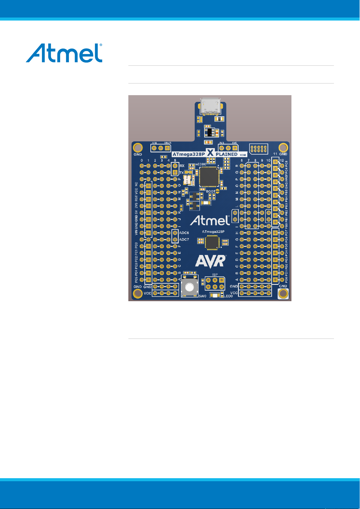
2.1 Board Overview
Figure 2-1. ATmega328P-XMINI Overview
2.2 Clock Distribution
The ATmega32U4 (mEDBG) has an external 16MHz XTAL.
The ATmega32U4 provides an external 16MHz clock to the ATmega328P (target).
2.3 Headers and Connectors
The board headers and connectors.
2.3.1 JTAG (J100)
J100 is the JTAG programming header typically used by the JTAGICE for programming of the ATmega32U4
(mEDBG).
Table 2-1. J100 JTAG Header
J100 pin Signal function
1 JTAG_TCK
ATmega328P Xplained Mini User Guide [USER GUIDE]
42287A-MCU-05/2014
8
Page 9

J100 pin Signal function
2 GND
3 JTAG_TDO
4 VCC (5V0)
5 JTAG_TMS
6 RESET
7 NC
8 NC
9 JTAG_TDI
10 GND
2.3.2 USB (J101)
J101 is a Micro-B USB connector connected to the embedded debugger (ATmega32U4).
Table 2-2. J101 USB Connector
J101 pin Function
1 VBUS
2 D-
3 D+
4 NC
5 GND
2.3.3 USART (J104)
The ATmega32U4 USART signals are available on J104 USART header.
The mEDBG CDC COM port is connected to these signals.
Table 2-3. J104 USART Header
J104 pin ATmega32U4 ATmega328P Function
1 - UART TXD PD3 PD1 TxD from ATmega32U4.
2 - UART RXD PD2 PD0 RxD to ATmega32U4.
2.3.4 Target Digital I/O (J200 and J201)
The J200 and J201 headers provide access to ATmega328P digital I/O pins.
Table 2-4. J200 I/O High Header
J200 pin &
ATmega328P pin Note
location
J200-1 PB0
J200-2 PB1
J200-3 PB2
J200-4 PB3
J200-5 PB4
J200-6 PB5/SCK Yellow USER LED D200 connected.
J200-7 GND
J200-8 AREF
J200-9 PC4/SDA TWI Serial Data.
ATmega328P Xplained Mini User Guide [USER GUIDE]
42287A-MCU-05/2014
9
Page 10

J200 pin &
ATmega328P pin Note
location
J200-10 PC5/SCL TWI Serial Clock.
Table 2-5. J201 I/O Low Header
J201 pin ATmega328P pin Note
J201-1 PD0/RxD Target USART Receive Pin.
J201-2 PD1/TxD Target USART Transmit Pin.
J201-3 PD2
J201-4 PD3
J201-5 PD4
J201-6 PD5
J201-7 PD6
J201-8 PD7
2.3.5 Target Analogue I/O (J203)
The ATmega328P analogue I/O pins are available in the J203 header.
Table 2-6. J200 Analogue Header
J203 pin & location ATmega328P pin
J203-1 PC0
J203-2 PC1
J203-3 PC2
J203-4 PC3
J203-5 PC4
J203-6 PC5
2.3.6 Power (J202, J300, J301)
The J300 and J301 headers enables selection of power sources and target supply power, the J202 header
enables connection to the power system.
Table 2-7. J202 Power Header
J202 pin Signal Description
1 NC.
2 VCC_TARGET ATmega328P supply voltage.
3 RESET_SENSE RESET from external source, monitored by the mEDBG, if pulled low the
4 VCC_P3V3 3.3V from on-board DC/DC converter (U300).
5 VCC_P5V0 Voltage from the selected power source, default VBUS.
6 GND
7 GND
8 VCC_VIN The externally connected power source if any.
2.3.6.1 Power supply configuration
The J300 and J301 headers enables Power supply configuration.
target RESET line will be pulled low. Possible to connect directly to the
target by assembling R212 and removing R110. Note: DebgWIRE will
then be disabled.
ATmega328P Xplained Mini User Guide [USER GUIDE]
42287A-MCU-05/2014
10
Page 11

Table 2-8. J300 Board External Power Selection
J300
Signal Description
pin
1 VCC_VBUS VBUS Pin of USB Connector via fuse F100, by default connected to VCC_P5V0
2 VCC_P5V0 Input voltage (4.3 to 16V) for the fixed-output voltage regulator (U300).
3 VCC_VIN Alternative power source for the board (4.3 to 16V), study U300 data sheet for
Table 2-9. J301 Board Power Supply Selection
J301
Signal Description
pin
1 VCC_P5V0 Board external power source as selected by J300, by default connected to
2 VCC_BOARD Power supply for ATmega32U4 and ATmega328P.
3 VCC_P3V3 Board 3.3V power supply from U300.
2.3.7 Target SPI (J204)
The J204 header enable direct connection to ISP for programming of the ATmega328P or to use the SPI bus to
connect external equipment.
Table 2-10. J204 SPI Header
J204 pin Function
1 MISO
2 VCC target (ATmega328P)
3 SCK
4 MOSI
5 RESET
6 GND
via R300.
detail requirements.
VCC_BOARD via R301.
2.3.8 Additional Target Signals
Signals not available in any of the headers or connectors are available in column 5.
ATmega328P Xplained Mini User Guide [USER GUIDE]
42287A-MCU-05/2014
11
Page 12

Table 2-11. Target uC I/O Signals not connected to any Connector or Header
ATmega328P pin Grid position
ADC6 H5
ADC7 G5
2.3.9 Extension headers
The marked area on the grid I7 to R8 can be used for strapping in a Xplained PRO extension header and a few
other headers based on the SPI bus.
The general bus connections for a Xplained PRO Extension board is indicated in the table below, detailed
wiring can be found in the selected Extension board documentation.
Table 2-12. Xplained Pro Extension Header
Pin Name Typical µC
signal
Typical
grid
Extension signal description
pin
1 ID NC Communication line to the ID chip on extension board.
2 GND Ground.
3 ADC(+) Analogue to digital converter, positive part of differential
ADC.
4 ADC(-) Analogue to digital converter, negative part of differential
ADC.
5 GPIO1 General purpose IO.
6 GPIO2 General purpose IO.
7 PWM(+) Pulse width modulation , alternatively positive part of
differential PWM. RESET to RF Extension board.
8 PWM(-) Pulse width modulation , alternatively positive part of
differential PWM.
9 IRQ/GPIO Interrupt request line from extension board.
10 SPI_SS_B/
GPIO
Slave select for SPI and/or general purpose I/O. Wake up
interrupt to RF extension (SLP_TR).
ATmega328P Xplained Mini User Guide [USER GUIDE]
42287A-MCU-05/2014
12
Page 13

Pin Name Typical µC
signal
Typical
grid
pin
11 TWI_SDA PC4/SDA M6 to
Q12
12 TWI_SCL PC5/SCL M9 to
R12
13 USART_RX PD0/RXD L6 to
A12
14 USART_TX PD1/TXD L9 to
B12
15 SPI_SS_A PB2/SS K6 to
K5.5
16 SPI_MOSI PB3/MOSI K9 to
K10
17 SPI_MISO PB4/MISO J6 to
J5.5
18 SPI_SCK PB5/SCK J9 to
J10
19 GND I6 to
GND
20 VCC I9 to
VCC
Extension signal description
Data line for two wire interface.
Clock line for two wire interface.
USART Input Pin from extension board, remove R107 if
used.
USART Output Pin to extension board, remove R108 if
used.
Slave select for Serial peripheral interface.
Master out slave in line of Serial peripheral interface.
Master in slave out line of Serial peripheral interface.
Clock for Serial peripheral interface.
Ground.
Power for extension board.
A number of Xplained PRO Extensions can be found at http://www.atmel.com/products/microcontrollers/avr/
xplainedpro.
Using Pin 11 to 20 enables connection of the 10pin connector used on the RZ600 wireless modules and the
10pin Xplained sensor modules.
2.4 Board GUI
2.4.1 LEDs
There are one LED available for use by application SW and one for the mEDBG.
Table 2-13. LEDs
LED Function
D100 - Green mEDBG, will light during enumeration.
D200 - Yellow ATmega328P pin 17 - PB5, also connected to mEDBG SCK for ISP programming, in 3-
state when not used by the ATmega32U4.
2.4.2 Button
A button is available for general use by application SW.
ATmega328P Xplained Mini User Guide [USER GUIDE]
42287A-MCU-05/2014
.
13
Page 14

Table 2-14. Button
Button Function ATmega328P pin
SW200 User defined high signal, press to ground
8 - PB7
(negate).
2.5 Factory Programmed Data
The ATmega328P Xplained Mini board comes with a demo program preprogrammed in the ATmega328P
FLASH using the external clock provided by the ATmega32U4.
The ATmega32U4 is preprogrammed with the mEDBG.
2.6 Errata
The following should be noted on revision 2 of the board ( A09-2323/2):
1. VCC on the Grid is not connected, VCC can be connected on grid N0 or from the ISP connector pin.2.
2. There is no capacitor on the 3V3 output if the board Vcc is powered from 5V.
ATmega328P Xplained Mini User Guide [USER GUIDE]
42287A-MCU-05/2014
14
Page 15

3. Document Revision History
Document
Date Comment
revision
42287A 05/2014 Initial document release
ATmega328P Xplained Mini User Guide [USER GUIDE]
42287A-MCU-05/2014
15
Page 16

Atmel Corporation 1600 Technology Drive, San Jose, CA 95110 USA T: (+1)(408) 441.0311 F: (+1)(408) 436.4200 | www.atmel.com
© 2014 Atmel Corporation. All rights reserved. / Rev.: 42287A-MCU-05/2014
Atmel®, Atmel logo and combinations thereof, Enabling Unlimited Possibilities®, AVR®, and others are registered trademarks or trademarks of Atmel
Corporation or its subsidiaries. Other terms and product names may be trademarks of others.
Disclaimer: The information in this document is provided in connection with Atmel products. No license, express or implied, by estoppel or otherwise, to any intellectual property right is granted
by this document or in connection with the sale of Atmel products. EXCEPT AS SET FORTH IN THE ATMEL TERMS AND CONDITIONS OF SALES LOCATED ON THE ATMEL WEBSITE,
ATMEL ASSUMES NO LIABILITY WHATSOEVER AND DISCLAIMS ANY EXPRESS, IMPLIED OR STATUTORY WARRANTY RELATING TO ITS PRODUCTS INCLUDING, BUT NOT
LIMITED TO, THE IMPLIED WARRANTY OF MERCHANTABILITY, FITNESS FOR A PARTICULAR PURPOSE, OR NON-INFRINGEMENT. IN NO EVENT SHALL ATMEL BE LIABLE FOR
ANY DIRECT, INDIRECT, CONSEQUENTIAL, PUNITIVE, SPECIAL OR INCIDENTAL DAMAGES (INCLUDING, WITHOUT LIMITATION, DAMAGES FOR LOSS AND PROFITS, BUSINESS
INTERRUPTION, OR LOSS OF INFORMATION) ARISING OUT OF THE USE OR INABILITY TO USE THIS DOCUMENT, EVEN IF ATMEL HAS BEEN ADVISED OF THE POSSIBILITY OF
SUCH DAMAGES. Atmel makes no representations or warranties with respect to the accuracy or completeness of the contents of this document and reserves the right to make changes to
specifications and products descriptions at any time without notice. Atmel does not make any commitment to update the information contained herein. Unless specifically provided otherwise,
Atmel products are not suitable for, and shall not be used in, automotive applications. Atmel products are not intended, authorized, or warranted for use as components in applications intended
to support or sustain life.
 Loading...