


 Loading...
MS2665C/MS2667C/MS2668C
Spectrum Analyzer
Service Manual
Third Edition
To ensure that this equipment is used safely, important safety items are explained in the MS2665C/MS2667C/MS2668C Spectrum Analyzer Operation Manual. This manual explains important service items related to service. Read both the operation manual and this manual, and keep both with the equipment.
Measuring Instruments Division
Measurement Group
ANRITSU CORPORATION
Document No.: M-W1335BE-3.0 |
i |

For Safety
For safety, do not open the equipment covers.
If repair is required, contact the sales representative, branch office, or agent at the telephone number and address given in this document or in the equipment operation manual.
Although not recommended by Anritsu Corporation, if it is really imperative to open the covers for emergency repair, take great care not to touch any dangerous parts. Always request repair by a trained engineer who understands the hazards.
Anritsu Corporation will not accept liability for any injuries sustained as a result of opening the equipment covers.
MS2665C/MS2667C/MS2668C
Spectrum Analyzer
Service Manual
15 |
April |
1998 |
(First Edition) |
2 |
March |
1999 |
(Third Edition) |
Copyright © 1998-1999, ANRITSU CORPORATION.
All rights reserved. No part of this manual may be reproduced without the prior written permission of the publisher.
The contents of this manual may be changed without prior notice.
ii
Part Names & Part Numbers
Please specify the part numbers shown in the parts list when making inquiries or when ordering parts. There may be a difference between the names of parts used in this manual and the parts actually used in the equipment or supplied for repair. This is because equivalent parts with the same functions, performance and reliability as the parts specified in the circuit diagrams and parts list have been used or supplied. Since the parts are equivalent, they have absolutely no adverse effect on the equipment specified functions, performance or reliability.
iii
iv
Table of Contents
For Safety ...................................................... |
ii |
|
Section 1 General......................................... |
1-1 |
|
Section 2 MS2665C ...................................... |
2-1 |
|
2.1 |
Overall Circuit description ............................................... |
2-2 |
2.2 |
Troubleshooting .............................................................. |
2-9 |
2.3 |
Mechanical configuration ................................................ |
2-31 |
Section 3 MS2667C ...................................... |
3-1 |
|
3.1 |
Overall Circuit description ............................................... |
3-2 |
3.2 |
Troubleshooting .............................................................. |
3-9 |
3.3 |
Mechanical configuration ................................................ |
3-33 |
Section 4 MS2668C ...................................... |
4-1 |
|
4.1 |
Overall Circuit description ............................................... |
4-2 |
4.2 |
Troubleshooting .............................................................. |
4-9 |
4.3 |
Mechanical configuration ................................................ |
4-27 |
Section 5 Firmware installation .................. |
5-1 |
|
Section 6 Performance test system ........... |
6-1 |
|
6.1 |
Required instruments ...................................................... |
6-2 |
6.2 |
Required software ........................................................... |
6-2 |
6.3 |
Test group 1 .................................................................... |
6-3 |
6.4 |
Test group 2 .................................................................... |
6-4 |
6.5 |
Test group 3 .................................................................... |
6-6 |
Section 7 Options ........................................ |
7-1 |
|
7.1 |
Introduction ..................................................................... |
7-2 |
7.2 |
Parts, PC board installation ............................................ |
7-3 |
7.3 |
Software setting .............................................................. |
7-7 |
7.4 |
Performance test ............................................................ |
7-11 |
I
II.
Section 1 General
This manual is for smooth maintenance and service work of the MS2665C/MS2667C/MS2668C Spectrum analyzer.
Refer to the separate operation manual for handling the instruments.
Our basic policy to the repair to the factory system, i.e. the defective instruments should be returned to Anritsu for repair.
However, it may be time consuming and some kinds of repairs can be easily done in the field.
Therefore, Anritsu allows only those who Anritsu has authorized to open the instrument and repair it.
As clearly stated in the WARRANTY statement, any unauthorized modification, repair, or attempt to repair will render the warranty void.
This service manual is composed of the following sections:
SECTION 2 MS2665C
This section contains the following items of MS2665C.
(1) Overall circuit description, (2) Troubleshooting procedure, (3) Mechanical configuration.
SECTION 3 MS2667C
This section contains the following items of MS2667C.
(1) Overall circuit description, (2) Troubleshooting procedure, (3) Mechanical configuration.
SECTION 4 MS2668C
This section contains the following items of MS2668C.
(1) Overall circuit description, (2) Troubleshooting procedure, (3) Mechanical configuration.
SECTION 5 Firmware installation
This section describes Firmware installation procedure.
SECTION 6 Performance test system
This section describes performance test procedure after repairing modules.
SECTION 7 Options
This section describes option installation procedures and performance test.
1-1
Section 1 General
1-2.
|
|
Section 2 |
MS2665C |
|
|
2.1 |
Overall Circuit description ......................................................... |
|
2-2 |
||
2.2 |
Troubleshooting |
......................................................................... |
|
2-9 |
|
|
2.2.1 |
Introduction .................................................................... |
|
2-9 |
|
|
|
2.2.1.1 |
Service kit........................................................ |
|
2-9 |
|
|
2.2.1.2 |
Required equipment ........................................ |
2-9 |
|
|
|
2.2.1.3 |
Circuit reference .............................................. |
|
2-10 |
|
2.2.2 |
Detecting faulty module ................................................. |
|
2-13 |
|
|
2.2.3 |
Disassembling cabinet ................................................... |
|
2-15 |
|
|
2.2.4 Replacement of faulty module ....................................... |
2-15 |
|||
|
2.2.5 Adjustment after module replacement ........................... |
2-16 |
|||
|
|
2.2.5.1 |
Reference crystal oscillator |
|
|
|
|
|
(Option 01) adjustment .................................... |
2-16 |
|
|
|
2.2.5.2 |
Sweep adjustment |
.......................................... |
2-18 |
|
|
2.2.5.3 IF1 (ATT), IF2 (AMP) adjustment .................... |
2-24 |
||
|
2.2.6 |
Assembling cabinet ........................................................ |
|
2-26 |
|
|
2.2.7 Checking items after assembling cabinet ...................... |
2-26 |
|||
|
2.2.8 |
Frequency response compensation .............................. |
2-27 |
||
2.3 |
Mechanical configuration ........................................................... |
|
2-31 |
||
|
2.3.1 |
Disassembling/Assembling cabinet ............................... |
2-31 |
||
|
2.3.2 Removing/Assembling units and PC boards ................. |
2-35 |
|||
|
2.3.3 |
Front unit disassembly/assembly ................................... |
2-39 |
||
|
2.3.4 A09 OPTION BASE disassembly/assembly .................. |
2-43 |
|||
2.3.5Removing/Assembling
A0501 HI-SPEED AD from A05 SCAN/AD .................... |
2-47 |
2-1
Section 2 MS2665C
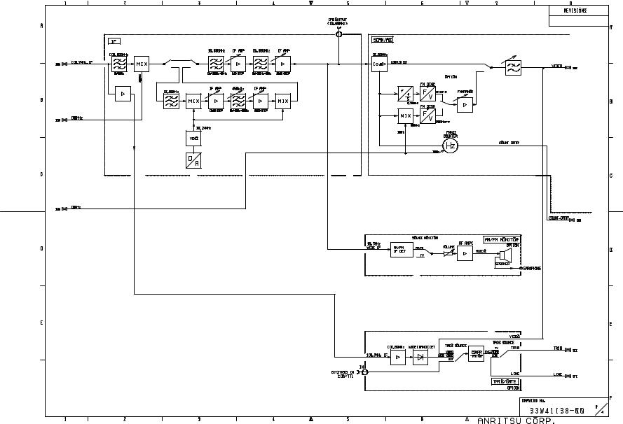
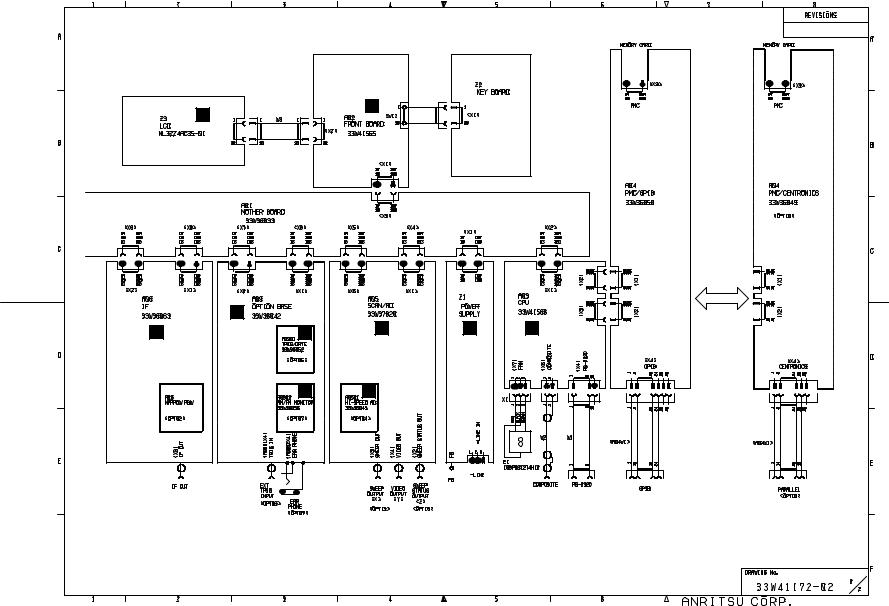
2.1 Overall Circuit description
MS2665C is a superheterodyne system scanning-type spectrum analyzer.
This section describes overall circuit of the MS2665C spectrum analyzer with its block diagram.
An RF input signal after passing through an RF switch and variable RF ATTN in 21 GHz S-ATT is switched by PIN diode switch in 21 GHz YTF/SW to two different signal routes depending on input RF frequency.
For an RF input frequency of 9 kHz to 3.1 GHz (termed as band 0), the signal passes through 3.2 GHz LPF and then to 1st mixer (1st MIX), where it is mixed with 1st local signal (4.1 GHz to 7.2 GHz) to generate 4110.69 MHz 1st IF signal. The 1st IF signal is then passed through an amplifier and image rejection filters, and fed to 2nd mixer (2nd MIX), where it is mixed with 4 GHz 2nd local signal to generate 110.69 MHz 2nd IF signal.
For an RF input frequency of 3.1 GHz to 21.2 GHz (band 1 to 3), the signal goes to YTF (YIG tuned filter) in 21 GHz YTF/ SW, and then to H. MIXER. In H. MIXER, the RF signal gets mixed with the 1st local signal (3.6 GHz to 7.5 GHz) to generate 689.31 MHz 1st IF signal.
This 1st IF signal is passed through a series of amplifiers and image rejection filters before further mixing with 800 MHz 2nd local signal to convert the signal to 110.69 MHz 2nd IF signal.
Depending on the active band of RF input, one of the two above 2nd IF signal is sent to IF section for further processing.
The 1st local signal generated at YTO (YIG tuned oscillator) is frequency-swept by scan signal from SCAN/AD section after phase-lock to reference signal (its frequency is 11 MHz to 14 MHz with the resolution of 1 Hz steps) generated on LOCAL-A section at the center frequency of its sweeping range, in normal sweep condition.
The YTO output is passed through an amplifier, and then divided into three paths with directional couplers. One of divided signal is fed to sampler circuit and the other are fed to the above mixers to frequency-convert.
In the sampler circuit, sampling signal (its frequency is 94 MHz to 106 MHz with the resolution of 1 MHz steps) generated on LOCAL-A section is frequency-multiplied, and then mixed with the YTO output to generate sampler IF signal with a frequency of 11 MHz to 14 MHz.
The sampler IF signal is compared with the reference signal of 11 MHz to 14 MHz at PFD.
The reference signal frequency (fREF) and the sampling signal frequency (fs) are controlled by CPU section according to the measuring frequency of the instrument, and set so that the center frequency of 1st local signal is fs * N ± fREF (, where N is an integer).
Meanwhile, the scan signal strength that is equivalent to frequency sweep width is controlled from LOCAL-A section.
The 2nd local signals of 4 GHz and 800 MHz are also phase-locked to 100 MHz VCXO signal, of which the frequency is also phase-locked to 10 MHz crystal oscillator (option 01).
In the instrument, a high accuracy 625 kHz signal is present for level accuracy calibration. This signal is generated by frequency-dividing the 10 MHz reference signal, and its power level is varied with 1 dB steps by CAL ATT.
Internal calibration operation being carried out, this calibrating signal is fed to the RF signal-route through the switch in 21 GHz S-ATT.
2-2
2.1 Overall Circuit description
At the IF section the incoming signal is divided into two paths. The main route leads to image rejection filters while the second, a highly attenuated feeler path signal is used for generation of wide band trigger signal in TRIG/GATE section ( option 06) situated on OPTION BASE board.
The main signal after passing through an image rejection filter is beat down to a 10.69 MHz signal using a 100 MHz reference signal. This signal is then sent to various Resolution Band Width (RBW) setting circuits.
For RBW setting of 30 Hz to 200 Hz the signal is frequency converted to 450 kHz using 10.24 MHz signal. After passing through the RBW circuits (Crystal filter circuits) the signal is up converted back to 10.69 MHz signal and passed through wider RBW setting circuits.
For RBW setting of 300 Hz to 3 MHz the signal is sent directly to wide RBW setting circuits without any frequency modifications.
The RBW processed signal is passed onto SCAN/AD section, where it passes through logarithmic amplifiers and then to a linear detector. This linear detected signal is passed through smoothing filters called Video Band Width Filters (VBW). This smoothed signal is then passed through Positive or Negative peak detection circuits and the output is converted to digital signal by a Analog to Digital Convertor (ADC) circuit.
The results are then written (in digital word format) to a Dual Port RAM through one of the ports.
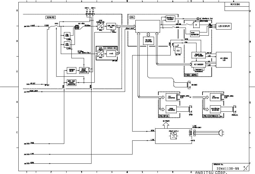
The CPU of the instrument on CPU section reads from the other port of Dual Port RAM and processes the data before displaying on the LCD screen. The CPU also controls various interface functions such as reading the Key Inputs or remote control commands received, and various outputs such as prints or plots of various data. The CPU also generates various commands required for controlling or setting of all hardware units inside the instrument.
FRONT BOARD section generates the KEY and rotary-knob encoder data, drives the LEDs, detects the power switch (PWR SW) setting, controls the power-supply On/Stby setting, and supplies power for the LCD backlight, etc.
2-3
Section 2 MS2665C
2-4

2.1 Overall Circuit description
2-5
Section 2 MS2665C
2-6
2.1 Overall Circuit description
2-7
Section 2 MS2665C
2-8
2.2 Troubleshooting
2.2 Troubleshooting
2.2.1 Introduction
2.2.1.1 Service kit
The ordering number of service kit is 34Y117630.
Table 2-2-1 Service kit
|
Name |
Quantity |
Drawing number |
Description |
|
Adjustment driver |
1 |
34Z99432 |
|
|
Adjustment driver |
1 |
34Z81433 |
|
|
Torque wrench |
1 |
34B35154 |
|
|
HRM554S |
2 |
NO. 1305 |
NP-SMAJ adapter |
|
HRM501 |
2 |
NO. 1305 |
SMAJ-SMAJ adapter |
|
HRM519 |
2 |
NO. 1305 |
SMAP-BNCJ adapter |
|
|
|
|
|
|
Extender cable |
3 |
34J92837F |
BNC-PJ-1.5, 27DP-LP-1.5, 300 mm |
|
Extender cable |
3 |
34J94207 |
27DP-BJ, 27DP-LP-1.5, 300 mm |
|
Extender cable |
2 |
S4J10001F |
BNC-P, 1000 mm |
|
Extender cable |
3 |
S4W10184C |
SMA-P-3T-NI (8), 300 mm |
|
|
|
|
|
|
Extender cable |
1 |
349J109862 |
for A08 LOCAL-A |
|
Extender cable |
1 |
34Y109639 |
for 3 GHz CONVERTER |
|
Extender cable |
1 |
34Y109632 |
for A05 SCAN/AD |
|
Extender cable |
1 |
34Y109632B |
for A09 OPTION BASE |
|
Extender cable |
2 |
34Y109632C |
for A09 OPTION BASE |
|
Extender cable |
2 |
34Y109632D |
for A05 SCAN/AD |
2.2.1.2 Required equipment
Table 2-2-2 shows the equipment to prepare for overall adjustment of the spectrum analyzer.
Table 2-2-2 Required equipment
Nomenclature |
Model number |
Manufacture |
Synthesized signal generator |
MG3633A |
Anritsu |
Frequency counter |
MF76A |
Anritsu |
Swept frequency synthesizer |
6769B |
Anritsu |
two Power meters |
ML4803A |
Anritsu |
Power sensor |
MA4701A |
Anritsu |
Power sensor |
MA4705A |
Anritsu |
Digital multimeter |
HP3478A |
Hewlett Packard |
GPIB interface board |
GPIB-PC2/2A |
National Instruments Corp. |
two 3 dB attenuators |
|
|
IBM-PC/AT compatible |
|
|
a printer |
|
|
2-9
Section 2 MS2665C
2.2.1.3 Circuit reference
This paragraph supplies the exchangeable module list of the spectrum analyzer with its overall circuit diagram.
Table 2-2-3 Exchange modules of the MS2665C
Schematic number |
Name |
Model number |
Ordering number |
Note |
1 |
A01 MOTHER BOARD |
322U12876 |
34Y106673 |
|
|
|
|
|
|
2 |
A02 FRONT BOARD |
322U14223 |
34Y118357 |
|
3 |
A03 CPU |
322U14225 |
34Y118358 |
|
|
|
|
|
|
4 |
A04 PMC/GPIB |
322U12853 |
34Y106693 |
|
5 |
A05 SCAN/AD |
34Y112923C |
34Y112923C |
|
6 |
A06 IF (B) |
322U13830 |
34Y106718 |
|
7 |
A08 LOCAL-A |
322U12849 |
34Y106679 |
|
8 |
3GHz CONVERTER |
34Y108179B |
34Y108179B |
|
9 |
A13 MICRO CONVERTER |
34Z110446C |
34Y110446C |
|
10 |
A14 1ST LO AMP |
34Z110447 |
34Y110447 |
|
|
|
|
|
|
11 |
21GHz S-ATT |
339H37752 |
339H37752 |
|
12 |
21GHz YTF/SW |
329H13289 |
329H13289 |
|
|
|
|
|
|
13 |
H.MIXER |
329H13290 |
329H13290 |
|
14 |
POWER SUPPLY UNIT |
34Z112975 |
34Z112975 |
|
15 |
TFT LCD MODULE |
NL3224AC35-01 |
No1256 |
|
16 |
A09 OPTION BASE |
322U12930 |
34Y106684 |
|
|
|
|
|
|
Options |
|
|
|
|
|
|
|
|
|
17 |
A0501 HI-SPEED AD |
332U36333 |
34Y106688 |
Option 04 |
|
|
|
|
|
18 |
A0901 TRIG/GATE |
322U12979 |
34Y106695 |
Option 06 |
|
|
|
|
|
19 |
A0902 AM/FM MONITOR |
322U12981 |
34Y106699 |
Option 07 |
20 |
A04 PMC/CENTRONICS |
34Y106692B |
34Y106692B |
Option 10 |
To identify a exchange module, a label printed “Model number” is pasted on module.
2-10
2.2 Troubleshooting
|
8 |
|
|
11 |
|
|
1 |
|
|
12 |
|
|
9 |
7 |
13 |
10 |
|
|
|
2-11
Section 2 MS2665C
2
15
4 |
|
20 |
|
16 |
6 |
18 |
|
19 |
5 |
17 |
14 |
3 |
2-12
2.2 Troubleshooting
2.2.2 Detecting faulty module
The flowchart shows the way to locate the faulty module among them.
POWER ON
LEDs come on?
The LCD comes on?
Fan Movement?
Key, Rotary knob come on?
Sweeping?
Trace Displayd When signal input?
Freq Display correct?
Level Display correct?
RBW Setting?
VBW Setting?
Input ATT Setting?
LOG/LIN Setting?
TRIG Setting?
Det mode Setting?
Display mode Setting?
Hardcopy possible?
Memory Backup?
(Yes)
Normal
No
No
No
No
No
No
No
No
No
No
No
No
No
No
No
No
No
[Location of faulty module]
 Fuse, A02 FRONT BOARD, POWER SUPPLY UNIT
 A03 CPU, TFT LCD MODULE, POWER SUPPLY UNIT
 A02 FRONT BOARD, POWER SUPPLY UNIT
 A02 FRONT BOARD, A03 CPU
 A05 SCAN/AD, A08 LOCAL-A, A03 CPU
3GHz CONVERTER, A13 MICRO CONVERTER, 21GHz S-ATT, 21GHz YTF/SW, H. MIXER
 A08 LOCAL-A, 3GHz CONVERTER
3GHz CONVERTER, A06 IF, A13 MICRO CONVERTER, 21GHz S-ATT, 21GHz YTF/SW, H. MIXER
 A06 IF
 A05 SCAN/AD
 3GHz CONVERTER
 A05 SCAN/AD
 A0902 TRIG/GATE
 A05 SCAN/AD
 A03 CPU
 A03 CPU
 A03 CPU
2-13
Section 2 MS2665C
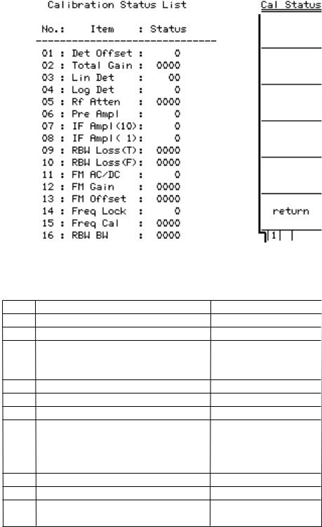
After executing internal calibration, you can locate the faulty module using “Cal Status” (as shown below). “Cal Status” can be displayed by the key operation : open the second page of Cal menu with “More” key, and press “F5” key.
If error occurred (Status value is not zero), the faulty module corresponding to each item is shown below :
|
NO. |
Error item (at the status is not zero ) |
Faulty module |
|
|
01 |
Det Offset |
A05 SCAN/AD |
|
|
02 |
Total Gain |
A06 IF |
|
|
03 |
Lin Det |
A05 SCAN/AD |
|
|
|
|
|
|
|
04 |
Log Det |
A05 SCAN/AD |
|
|
|
|
|
|
|
05 |
RF Atten |
HR S-ATT |
|
|
06 |
Pre Ampl |
3 GHz PRE AMP |
|
|
07 |
IF Ampl (10) |
A06 IF |
|
|
08 |
IF Ampl (1) |
A06 IF |
|
|
09 |
RBW Loss (T) |
A06 IF |
|
|
|
|
|
|
|
10 |
RBW Loss (F) |
A06 IF |
|
|
|
|
|
|
|
11 |
FM DC/AC |
A0902 AM/FM MONITOR |
|
|
|
|
|
|
|
12 |
FM Gain |
A0902 AM/FM MONITOR |
|
|
13 |
FM Offset |
A0902 AM/FM MONITOR |
|
|
14 |
Freq Lock |
A08 LOCAL-A |
|
|
15 |
Freq Cal |
A08 LOCAL-A |
|
|
|
|
|
|
|
16 |
RBW BW |
A06 IF |
|
2-14
2.2 Troubleshooting
2.2.3 Disassembling cabinet
Refer to 2.3.1.
2.2.4 Replacement of faulty module
Refer to 2.3.2 to 2.3.5.
2-15
Section 2 MS2665C
2.2.5 Adjustment after module replacement
This paragraph describes the overall adjustment required after replacement of any modules in following Table. Look for modules which you replaced in Table. Please carry out work corresponding to module which you replaced. This adjustment is not necessary, if the module you replaced does not belong to the following Table.
Replaced module |
|
|
|
A08 LOCAL-A |
Carry out 2.2.5.1 and 2.2.5.2. |
|
|
3GHz CONVERTER |
Carry out 2.2.5.2 and 2.2.5.3. |
A13 MICRO CONVERTER |
|
21GHz YTF/SW |
|
|
|
2.2.5.1 Reference crystal oscillator (option 01) adjustment
Remark :
Before this adjustment, leave the spectrum analyzer power-on at least for 6 to 7 hours. This adjustment needs a very high accuracy frequency standard (10 MHz).
Required equipment :
(1)MG3633A Synthesized signal generator
(2)MF76A Frequency counter
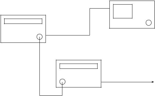
Setup :
to Ref Out |
The spectrum analyzer |
|
|
on the rear |
|
MG3633A
to Ref Input on the rear
Output
MF76A
to 10 MHz In
on the rear to 10 MHz standard signal
Input
Fig. 2-2-1
2-16
2.2 Troubleshooting
(1)Connect the spectrum analyzer Buff Out (on its rear panel) to MG3633A REF INPUT (on its rear panel).
(2)Connect the MG3633A OUTPUT to MF76A Input.
(3)Connect the MF76A EREQ STD 10 MHz IN (on its rear panel) to 10 MHz standard signal. And set the EXT/INT selector switch to EXT.
Procedure :
(1)Set the MG3633A output to : Center frequency, 1 GHz (CW) Output level, 0 dBm
(2)Set the MF76A to resolution 1 Hz.
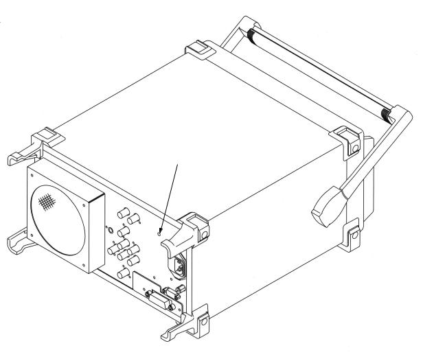
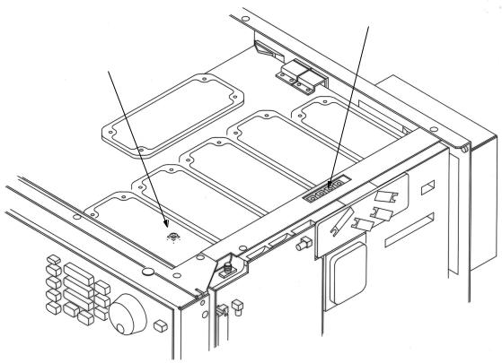
(3)Adjust the “Reference Adjust Screw (Multi-turn potentiometer)” visible through the hole provided on the rear panel (refer to Fig. 2-2-2) to make the MF76A reading 1,000,000,000 Hz ± 5 Hz.
Reference Adjust Screw
Fig. 2-2-2 The location of an adjuster of Reference crystal oscillator
2-17
Section 2 MS2665C
2.2.5.2 Sweep adjustment
Required equipment :
(1)6769B Swept frequency synthesizer,
(2)MG3633A Synthesized signal generator,
(3)HP3478A Digital multimeter.
Setup for the procedure (1), (2) :
MG3633A |
The spectrum analyzer |
Output |
RF Input |
Fig. 2-2-3
Connect the spectrum analyzer RF Input to MG3633A OUTPUT.
Setup for the procedure (3) :
(1)Connect digital multimeter HI input to the TP4 terminal on A1306 MICRO DRIVER PC board attached to A13 MICRO CONVERTER.
(2)Connect digital multimeter LO input to the spectrum analyzer’s common.
Setup for the procedure (4), (5), (6) :
6769B |
The spectrum analyzer |
RF Output |
RF Input |
Fig. 2-2-4
(1) Connect the spectrum analyzer RF Input to 6769B RF OUTPUT.
2-18
2.2 Troubleshooting
Procedure :
(1)Local sweep adjustment
Initialize the spectrum analyzer and the MG3633A.
1)Set the spectrum analyzer to : Center frequency, 100 MHz Span, 100 kHz
Set the MG3633A output to : LEVEL, -10 dBm
Frequency, 100 MHz (CW)
Press “→ CF” key of the spectrum analyzer.
2)Set the MG3633A output frequency to 99.96 MHz (CW).
On the spectrum analyzer, press “Peak Search” key, and set the marker function to delta maker mode (Press “Marker” key and press “F2” key).
3)Set the MG3633A output frequency to 100.04 MHz (CW).
On the spectrum analyzer, press “Peak Search” key, and read the frequency difference between 99.96 MHz input and 100.04 MHz input.
4)Adjust the variable resistor R96 on A08 LOCAL-A (refer to Fig. 2-2-5) until the reading of frequency difference becomes 80 kHz ± 200 Hz, to repeat the procedure 2), 3).
(2)YTO FM sweep adjustment Initialize the spectrum analyzer.
1)Set the spectrum analyzer to : Center frequency, 1000 MHz Span, 10 MHz
Set the MG3633A output to :
Frequency, 1000 MHz (CW)
Press “→ CF” key of the spectrum analyzer.
2)Set the MG3633A output frequency to 996 MHz (CW).
On the spectrum analyzer, press “Peak Search” key, and set the marker function to delta maker mode (Press “Marker” key and press “F2” key).
3)Set the MG3633A output frequency to 1004 MHz (CW).
On the spectrum analyzer, press “Peak Search” key, and read the frequency difference between 996 MHz input and 1004 MHz input.
4)Adjust the variable resistor R53 on 3GHz CONVERTER (refer to Fig. 2-2-5) until the reading of frequency difference becomes 8 MHz ± 40 kHz, to repeat the procedure 2), 3).
2-19
Section 2 MS2665C
(3)YTF tuning DAC adjustment
1)Turn the spectrum analyzer on, while pushing “0” key, and initialize the spectrum analyzer.
2)Set the spectrum analyzer to zero Span.
3)Enter Cal menu by pushing “Shift + 0” keys. Open the second page of the Cal menu, and enter Maintenance menu with “F6” key. Enter RF/Micro converter maintenance menu with “F2” key, and open the 6th page of the menu (Press “More” key 5 times).
4)Set YTF Pre-tuning value to 3600 by pushing “F2” key (assigned YTF Pre-tuning function) and data keys.
5)Adjust the variable resistor R60 on the A13 MICRO CONVERTER (refer to Fig. 2-2-6) to make multimeter reading -3.600 ± 0.005 Volts.
6)Set YTF Pre-tuning value to 7600 by pushing “F2” key.
7)Adjust the variable resistor R57 on the A13 MICRO CONVERTER (refer to Fig. 2-2-6) to make multimeter reading -7.600 ± 0.005 Volts.
8)Repeat the procedure 4), 5), 6), 7) until you get the required voltage corresponding to each YTF Pre-tuning value.
(4)YTF tuning adjustment
1)Initialize the spectrum analyzer (Press “Preset” key and press “F1” key).
2)After 5 seconds waiting, set the spectrum analyzer to : Center frequency, 2.92 GHz
Zero Span
Set the 6769B output to : Frequency, 2.92 GHz (CW) RF LEVEL, -20 dBm
3)Enter Cal menu by pushing “Shift + 0” keys. Enter Pre-selector Tuning menu with “F6” key.
4)Press “F2” key and set Pre-selector bias value to 0, using the data keys or the knob on the front panel.
5)Adjust the variable resistor R22 on A13 MICRO CONVERTER (refer to Fig. 2-2-6) to make displayed signal level maximum.
6)Set the spectrum analyzer to : Center frequency, 6.4 GHz Zero Span
Set the 6769B output to : Frequency, 6.4 GHz (CW) RF LEVEL, -20 dBm
2-20
2.2 Troubleshooting
7)Enter Cal menu by pushing “Shift + 0” keys. Enter Pre-selector Tuning menu with “F6” key.
8)Press “F2” key and set Pre-selector bias value to 0, using the data keys or the knob on the front panel.
9)Adjust the variable resistor R31 on A13 MICRO CONVERTER (refer to Fig. 2-2-6) to make displayed signal level maximum.
10)Put the screw of the variable resistor R68 on A13 MICRO CONVERTER (refer to Fig. 2-2-6) center in its rotation range.
(5)YTO main sweep adjustment
Initialize the spectrum analyzer and the 6769B.
1)Set the spectrum analyzer to : Center frequency, 1.5 GHz Span, 3 GHz
Set the 6769B output to : RF LEVEL, -10 dBm
Frequency, 1.5 GHz (CW)
Press “→ CF” key of the spectrum analyzer.
2)Set the 6769B output frequency to 300 MHz.
On the spectrum analyzer, press “Peak Search” key, and set the marker function to delta marker mode (Press “Marker” key and press “F2” key).
3)Set the 6769B output frequency to 2.7 GHz.
On the spectrum analyzer, press “Peak Search” key, and read the frequency difference between 300 MHz input and 2.7 GHz input.
4)Adjust the variable resistor R57 on 3GHz CONVERTER (refer to Fig. 2-2-5) until the reading of frequency difference becomes 2.4 GHz ± 6 MHz, to repeat the procedure 2), 3).
5)Initialize the spectrum analyzer (Press “Preset” key and press “F1” key). Set the 6769B to :
Frequency, 14.2 GHz (CW) RF LEVEL, -20 dBm
6)Set Pre-selector bias value to 0, according to above-mentioned procedure.
7)Press “Peak Search” key to place marker indicator on the top of 14.2 GHz signal.
8)Adjust the variable resistors R63 and R64 on A13 MICRO CONVERTER (refer to Fig. 2-2-6) to make the signal level maximum, i.e. increase the level roughly with R63, and then using R64, make it exactly maximum.
2-21
Section 2 MS2665C
(6)Confirmation of YTF tuning
Initialize the spectrum analyzer and the 6769B.
1)Set the spectrum analyzer to : Start frequency, 3 GHz
Stop frequency, 21 GHz Log Scale, 2 dB
Storage Max Hold (Press “A, B” key, press “F5” key and “F2” key).
2)Set the 6769B to : F1 frequency, 3 GHz
F2 frequency, 21 GHz RF LEVEL, -10 dBm Analog sweep ON Sweep time, 50 seconds
3)Confirm that the waveform on the analyzer’s display is flat, after the 6769B finishes its 50-second sweeping.
R53, R57
R96
Fig. 2-2-5 The location of adjusters on A08 LOCAL-A and 3GHz CONVERTER
2-22
Loading...