

Page 1

MS2665C/MS2667C/MS2668C
Spectrum Analyzer
Service Manual
Third Edition
To ensure that this equipment is used safely, important safety items are explained in the
MS2665C/MS2667C/MS2668C Spectrum Analyzer
Operation Manual. This manual explains important service items related to service. Read both
the operation manual and this manual, and keep
both with the equipment.
Measuring Instruments Division
Measurement Group
ANRITSU CORPORATION
Document No.: M-W1335BE-3.0
i
Page 2

For Safety
For safety, do not open the equipment covers.
If repair is required, contact the sales representative, branch office, or agent at the
telephone number and address given in this document or in the equipment operation manual.
Although not recommended by Anritsu Corporation, if it is really imperative to
open the covers for emergency repair, take great care not to touch any dangerous
parts. Always request repair by a trained engineer who understands the hazards.
Anritsu Corporation will not accept liability for any injuries sustained as a result of
opening the equipment covers.
MS2665C/MS2667C/MS2668C
Spectrum Analyzer
Service Manual
15 April 1998 (First Edition)
2 March 1999 (Third Edition)
Copyright © 1998-1999, ANRITSU CORPORATION.
All rights reserved. No part of this manual may be reproduced without the prior written permission of the
publisher.
The contents of this manual may be changed without prior notice.
ii
Page 3

Part Names & Part Numbers
Please specify the part numbers shown in the parts list when making inquiries or when ordering
parts. There may be a difference between the names of parts used in this manual and the parts
actually used in the equipment or supplied for repair. This is because equivalent parts with the
same functions, performance and reliability as the parts specified in the circuit diagrams and
parts list have been used or supplied. Since the parts are equivalent, they have absolutely no
adverse effect on the equipment specified functions, performance or reliability.
iii
Page 4

iv
Page 5

Table of Contents
For Safety ...................................................... ii
Section 1 General......................................... 1-1
Section 2 MS2665C ...................................... 2-1
2.1 Overall Circuit description............................................... 2-2
2.2 Troubleshooting .............................................................. 2-9
2.3 Mechanical configuration ................................................ 2-31
Section 3 MS2667C ...................................... 3-1
3.1 Overall Circuit description............................................... 3-2
3.2 Troubleshooting .............................................................. 3-9
3.3 Mechanical configuration ................................................ 3-33
Section 4 MS2668C ...................................... 4-1
4.1 Overall Circuit description............................................... 4-2
4.2 Troubleshooting .............................................................. 4-9
4.3 Mechanical configuration ................................................ 4-27
Section 5 Firmware installation .................. 5-1
Section 6 Performance test system ........... 6-1
6.1 Required instruments...................................................... 6-2
6.2 Required software........................................................... 6-2
6.3 Test group 1.................................................................... 6-3
6.4 Test group 2.................................................................... 6-4
6.5 Test group 3.................................................................... 6-6
Section 7 Options ........................................ 7-1
7.1 Introduction ..................................................................... 7-2
7.2 Parts, PC board installation ............................................ 7-3
7.3 Software setting .............................................................. 7-7
7.4 Performance test ............................................................ 7-11
I
Page 6

II
.
Page 7

Section 1 General
This manual is for smooth maintenance and service work of the MS2665C/MS2667C/MS2668C Spectrum analyzer.
Refer to the separate operation manual for handling the instruments.
Our basic policy to the repair to the factory system, i.e. the defective instruments should be returned to Anritsu for repair.
However, it may be time consuming and some kinds of repairs can be easily done in the field.
Therefore, Anritsu allows only those who Anritsu has authorized to open the instrument and repair it.
As clearly stated in the WARRANTY statement, any unauthorized modification, repair, or attempt to repair will render the
warranty void.
This service manual is composed of the following sections:
SECTION 2 MS2665C
This section contains the following items of MS2665C.
(1) Overall circuit description, (2) Troubleshooting procedure, (3) Mechanical configuration.
SECTION 3 MS2667C
This section contains the following items of MS2667C.
(1) Overall circuit description, (2) Troubleshooting procedure, (3) Mechanical configuration.
SECTION 4 MS2668C
This section contains the following items of MS2668C.
(1) Overall circuit description, (2) Troubleshooting procedure, (3) Mechanical configuration.
SECTION 5 Firmware installation
This section describes Firmware installation procedure.
SECTION 6 Performance test system
This section describes performance test procedure after repairing modules.
SECTION 7 Options
This section describes option installation procedures and performance test.
1-1
Page 8

Section 1 General
1-2.
Page 9

Section 2 MS2665C
2.1 Overall Circuit description ......................................................... 2-2
2.2 Troubleshooting......................................................................... 2-9
2.2.1 Introduction .................................................................... 2-9
2.2.1.1 Service kit........................................................ 2-9
2.2.1.2 Required equipment........................................ 2-9
2.2.1.3 Circuit reference.............................................. 2-10
2.2.2 Detecting faulty module ................................................. 2-13
2.2.3 Disassembling cabinet................................................... 2-15
2.2.4 Replacement of faulty module ....................................... 2-15
2.2.5 Adjustment after module replacement ........................... 2-16
2.2.5.1 Reference crystal oscillator
(Option 01) adjustment.................................... 2-16
2.2.5.2 Sweep adjustment .......................................... 2-18
2.2.5.3 IF1 (ATT), IF2 (AMP) adjustment.................... 2-24
2.2.6 Assembling cabinet........................................................ 2-26
2.2.7 Checking items after assembling cabinet ...................... 2-26
2.2.8 Frequency response compensation .............................. 2-27
2.3 Mechanical configuration........................................................... 2-31
2.3.1 Disassembling/Assembling cabinet ............................... 2-31
2.3.2 Removing/Assembling units and PC boards ................. 2-35
2.3.3 Front unit disassembly/assembly................................... 2-39
2.3.4 A09 OPTION BASE disassembly/assembly .................. 2-43
2.3.5 Removing/Assembling
A0501 HI-SPEED AD from A05 SCAN/AD.................... 2-47
2-1
Page 10

Section 2 MS2665C
2.1 Overall Circuit description
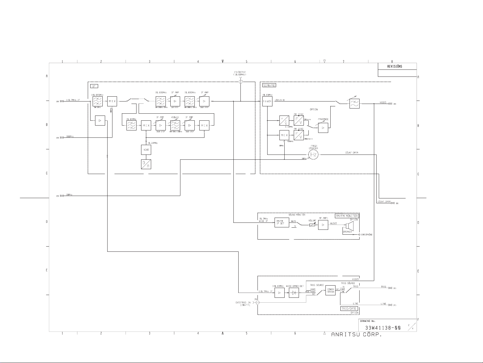
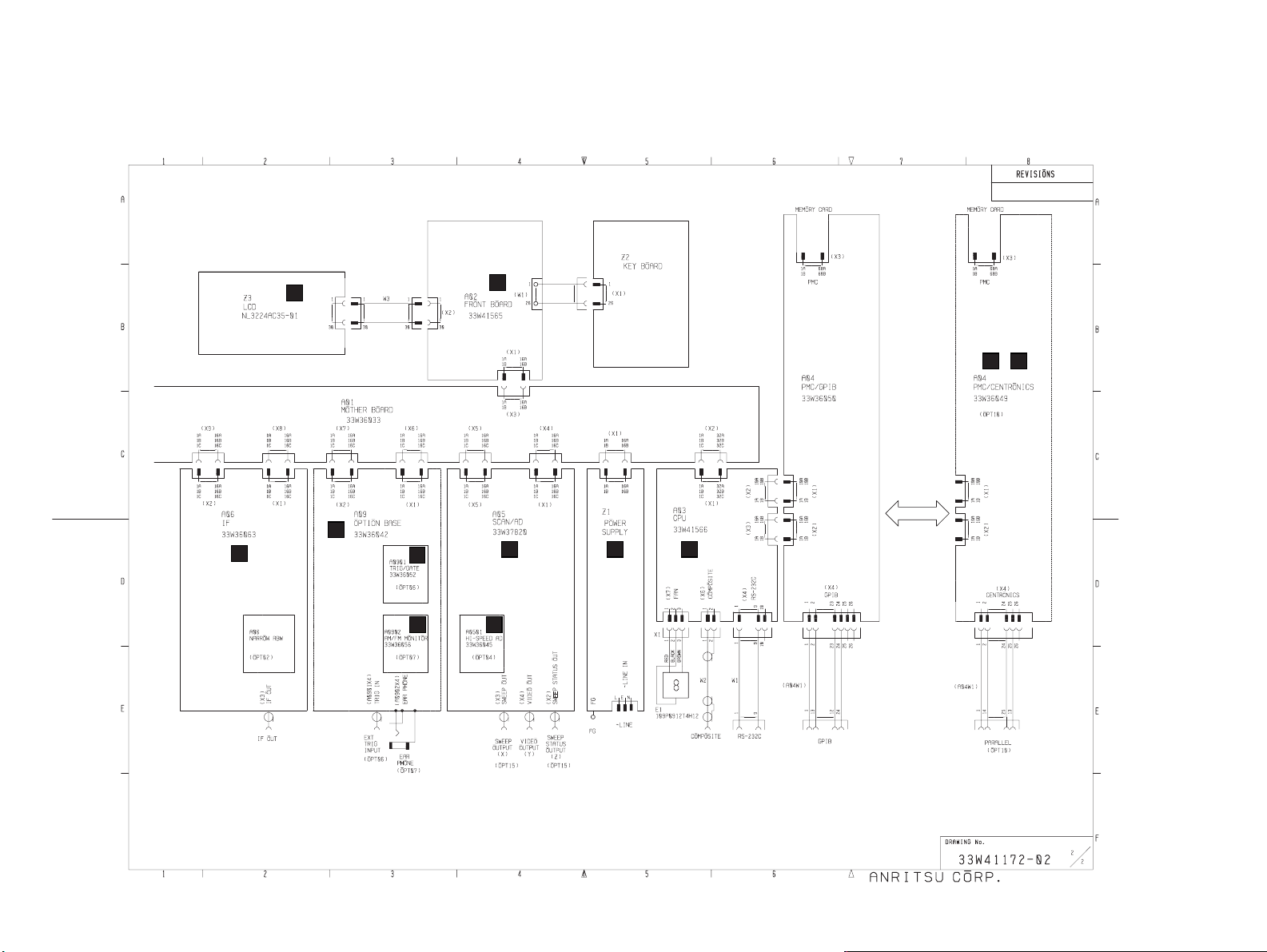
MS2665C is a superheterodyne system scanning-type spectrum analyzer.
This section describes overall circuit of the MS2665C spectrum analyzer with its block diagram.
An RF input signal after passing through an RF switch and variable RF ATTN in 21 GHz S-ATT is switched by PIN diode
switch in 21 GHz YTF/SW to two different signal routes depending on input RF frequency.
For an RF input frequency of 9 kHz to 3.1 GHz (termed as band 0), the signal passes through 3.2 GHz LPF and then to 1st
mixer (1st MIX), where it is mixed with 1st local signal (4.1 GHz to 7.2 GHz) to generate 4110.69 MHz 1st IF signal.
The 1st IF signal is then passed through an amplifier and image rejection filters, and fed to 2nd mixer (2nd MIX), where it
is mixed with 4 GHz 2nd local signal to generate 110.69 MHz 2nd IF signal.
For an RF input frequency of 3.1 GHz to 21.2 GHz (band 1 to 3), the signal goes to YTF (YIG tuned filter) in 21 GHz YTF/
SW, and then to H. MIXER. In H. MIXER, the RF signal gets mixed with the 1st local signal (3.6 GHz to 7.5 GHz) to
generate 689.31 MHz 1st IF signal.
This 1st IF signal is passed through a series of amplifiers and image rejection filters before further mixing with 800 MHz
2nd local signal to convert the signal to 110.69 MHz 2nd IF signal.
Depending on the active band of RF input, one of the two above 2nd IF signal is sent to IF section for further processing.
The 1st local signal generated at YTO (YIG tuned oscillator) is frequency-swept by scan signal from SCAN/AD section
after phase-lock to reference signal (its frequency is 11 MHz to 14 MHz with the resolution of 1 Hz steps) generated on
LOCAL-A section at the center frequency of its sweeping range, in normal sweep condition.
The YTO output is passed through an amplifier, and then divided into three paths with directional couplers. One of divided
signal is fed to sampler circuit and the other are fed to the above mixers to frequency-convert.
In the sampler circuit, sampling signal (its frequency is 94 MHz to 106 MHz with the resolution of 1 MHz steps) generated
on LOCAL-A section is frequency-multiplied, and then mixed with the YTO output to generate sampler IF signal with a
frequency of 11 MHz to 14 MHz.
The sampler IF signal is compared with the reference signal of 11 MHz to 14 MHz at PFD.
The reference signal frequency (fREF) and the sampling signal frequency (fs) are controlled by CPU section according to
the measuring frequency of the instrument, and set so that the center frequency of 1st local signal is fs * N ± fREF (, where
N is an integer).
Meanwhile, the scan signal strength that is equivalent to frequency sweep width is controlled from LOCAL-A section.
The 2nd local signals of 4 GHz and 800 MHz are also phase-locked to 100 MHz VCXO signal, of which the frequency is
also phase-locked to 10 MHz crystal oscillator (option 01).
In the instrument, a high accuracy 625 kHz signal is present for level accuracy calibration. This signal is generated by
frequency-dividing the 10 MHz reference signal, and its power level is varied with 1 dB steps by CAL ATT.
Internal calibration operation being carried out, this calibrating signal is fed to the RF signal-route through the switch in 21
GHz S-ATT.
2-2
Page 11

2.1 Overall Circuit description
At the IF section the incoming signal is divided into two paths. The main route leads to image rejection filters while the
second, a highly attenuated feeler path signal is used for generation of wide band trigger signal in TRIG/GATE section (
option 06) situated on OPTION BASE board.
The main signal after passing through an image rejection filter is beat down to a 10.69 MHz signal using a 100 MHz
reference signal. This signal is then sent to various Resolution Band Width (RBW) setting circuits.
For RBW setting of 30 Hz to 200 Hz the signal is frequency converted to 450 kHz using 10.24 MHz signal. After passing
through the RBW circuits (Crystal filter circuits) the signal is up converted back to 10.69 MHz signal and passed through
wider RBW setting circuits.
For RBW setting of 300 Hz to 3 MHz the signal is sent directly to wide RBW setting circuits without any frequency
modifications.
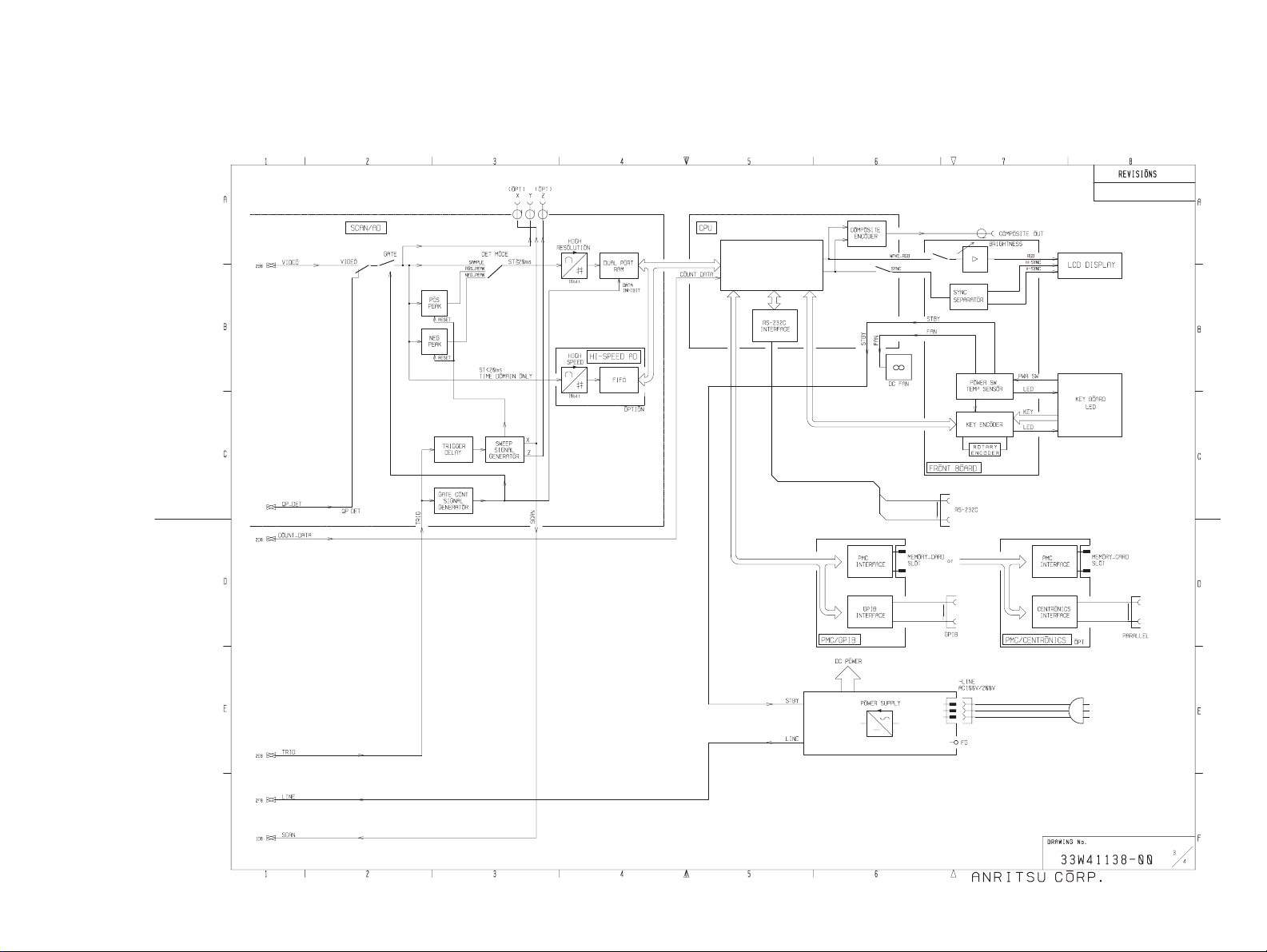
The RBW processed signal is passed onto SCAN/AD section, where it passes through logarithmic amplifiers and then to a
linear detector. This linear detected signal is passed through smoothing filters called Video Band Width Filters (VBW).
This smoothed signal is then passed through Positive or Negative peak detection circuits and the output is converted to
digital signal by a Analog to Digital Convertor (ADC) circuit.
The results are then written (in digital word format) to a Dual Port RAM through one of the ports.
The CPU of the instrument on CPU section reads from the other port of Dual Port RAM and processes the data before
displaying on the LCD screen. The CPU also controls various interface functions such as reading the Key Inputs or remote
control commands received, and various outputs such as prints or plots of various data. The CPU also generates various
commands required for controlling or setting of all hardware units inside the instrument.
FRONT BOARD section generates the KEY and rotary-knob encoder data, drives the LEDs, detects the power switch
(PWR SW) setting, controls the power-supply On/Stby setting, and supplies power for the LCD backlight, etc.
2-3
Page 12

Section 2 MS2665C
2-4
Page 13

2.1 Overall Circuit description
2-5
Page 14
Section 2 MS2665C
2-6
Page 15
2.1 Overall Circuit description
2-7
Page 16
Section 2 MS2665C
2-8
Page 17
2.2 Troubleshooting
2.2.1 Introduction
2.2.1.1 Service kit
The ordering number of service kit is 34Y117630.
Table 2-2-1 Service kit
Name Quantity Drawing number Description
Adjustment driver
Adjustment driver
Torque wrench
HRM554S
HRM501
HRM519
1
1
1
2
2
2
34Z99432
34Z81433
34B35154
NO. 1305
NO. 1305
NO. 1305
2.2 Troubleshooting
NP-SMAJ adapter
SMAJ-SMAJ adapter
SMAP-BNCJ adapter
Extender cable
Extender cable
Extender cable
Extender cable
Extender cable
Extender cable
Extender cable
Extender cable
Extender cable
Extender cable
3
3
2
3
1
1
1
1
2
2
34J92837F
34J94207
S4J10001F
S4W10184C
349J109862
34Y109639
34Y109632
34Y109632B
34Y109632C
34Y109632D
BNC-PJ-1.5, 27DP-LP-1.5, 300 mm
27DP-BJ, 27DP-LP-1.5, 300 mm
BNC-P, 1000 mm
SMA-P-3T-NI (8), 300 mm
for A08 LOCAL-A
for 3 GHz CONVERTER
for A05 SCAN/AD
for A09 OPTION BASE
for A09 OPTION BASE
for A05 SCAN/AD
2.2.1.2 Required equipment
Table 2-2-2 shows the equipment to prepare for overall adjustment of the spectrum analyzer.
Table 2-2-2 Required equipment
ManufactureNomenclature
Anritsu
Anritsu
Anritsu
Anritsu
Anritsu
Anritsu
Hewlett Packard
National Instruments Corp.
Synthesized signal generator
Frequency counter
Swept frequency synthesizer
two Power meters
Power sensor
Power sensor
Digital multimeter
GPIB interface board
two 3 dB attenuators
IBM-PC/AT compatible
a printer
Model number
MG3633A
MF76A
6769B
ML4803A
MA4701A
MA4705A
HP3478A
GPIB-PC2/2A
2-9
Page 18

Section 2 MS2665C
2.2.1.3 Circuit reference
This paragraph supplies the exchangeable module list of the spectrum analyzer with its overall circuit diagram.
Table 2-2-3 Exchange modules of the MS2665C
Schematic number
1
2
3
4
5
6
7
8
9
10
11
12
13
14
15
16
Options
17
18
19
20
Name Model number Ordering number Note
A01 MOTHER BOARD
A02 FRONT BOARD
A03 CPU
A04 PMC/GPIB
A05 SCAN/AD
A06 IF (B)
A08 LOCAL-A
3GHz CONVERTER
A13 MICRO CONVERTER
A14 1ST LO AMP
21GHz S-ATT
21GHz YTF/SW
H.MIXER
POWER SUPPLY UNIT
TFT LCD MODULE
A09 OPTION BASE
A0501 HI-SPEED AD
A0901 TRIG/GATE
A0902 AM/FM MONITOR
A04 PMC/CENTRONICS
322U12876
322U14223
322U14225
322U12853
34Y112923C
322U13830
322U12849
34Y108179B
34Z110446C
34Z110447
339H37752
329H13289
329H13290
34Z112975
NL3224AC35-01
322U12930
332U36333
322U12979
322U12981
34Y106692B
34Y106673
34Y118357
34Y118358
34Y106693
34Y112923C
34Y106718
34Y106679
34Y108179B
34Y110446C
34Y110447
339H37752
329H13289
329H13290
34Z112975
No1256
34Y106684
34Y106688
34Y106695
34Y106699
34Y106692B
Option 04
Option 06
Option 07
Option 10
To identify a exchange module, a label printed “Model number” is pasted on module.
2-10
Page 19

2.2 Troubleshooting
11
12
10
13
8
11
1
12
9
13
10
7
2-11
Page 20
Section 2 MS2665C
15
16
18
19
17
14
20
15
16
6
18
19
2
4 20
5
17
14
3
2-12
Page 21
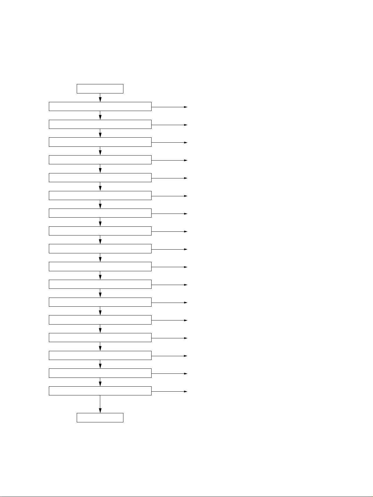
2.2.2 Detecting faulty module
The flowchart shows the way to locate the faulty module among them.
2.2 Troubleshooting
POWER ON
LEDs come on?
The LCD comes on?
Fan Movement?
Key, Rotary knob come on?
Sweeping?
Trace Displayd When signal input?
Freq Display correct?
Level Display correct?
RBW Setting?
VBW Setting?
No
No
No
No
No
No
No
No
No
No
[Location of faulty module]
Fuse, A02 FRONT BOARD, POWER SUPPLY UNIT
A03 CPU, TFT LCD MODULE, POWER SUPPLY UNIT
A02 FRONT BOARD, POWER SUPPLY UNIT
A02 FRONT BOARD, A03 CPU
A05 SCAN/AD, A08 LOCAL-A, A03 CPU
3GHz CONVERTER, A13 MICRO CONVERTER,
21GHz S-ATT, 21GHz YTF/SW, H. MIXER
A08 LOCAL-A, 3GHz CONVERTER
3GHz CONVERTER, A06 IF, A13 MICRO CONVERTER,
21GHz S-ATT, 21GHz YTF/SW, H. MIXER
A06 IF
A05 SCAN/AD
Input A TT Setting?
LOG/LIN Setting?
TRIG Setting?
Det mode Setting?
Display mode Setting?
Hardcopy possible?
Memory Backup?
(Yes)
Normal
No
No
No
No
No
No
No
3GHz CONVERTER
A05 SCAN/AD
A0902 TRIG/GA TE
A05 SCAN/AD
A03 CPU
A03 CPU
A03 CPU
2-13
Page 22
Section 2 MS2665C
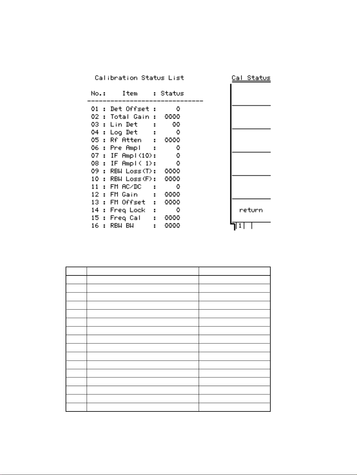
After executing internal calibration, you can locate the faulty module using “Cal Status” (as shown below). “Cal Status”
can be displayed by the key operation : open the second page of Cal menu with “More” key, and press “F5” key.
If error occurred (Status value is not zero), the faulty module corresponding to each item is shown below :
NO.
01
02
03
04
05
06
07
08
09
10
11
12
13
14
15
16
Error item (at the status is not zero )
Det Offset
Total Gain
Lin Det
Log Det
RF Atten
Pre Ampl
IF Ampl (10)
IF Ampl (1)
RBW Loss (T)
RBW Loss (F)
FM DC/AC
FM Gain
FM Offset
Freq Lock
Freq Cal
RBW BW
Faulty module
A05 SCAN/AD
A06 IF
A05 SCAN/AD
A05 SCAN/AD
HR S-ATT
3 GHz PRE AMP
A06 IF
A06 IF
A06 IF
A06 IF
A0902 AM/FM MONITOR
A0902 AM/FM MONITOR
A0902 AM/FM MONITOR
A08 LOCAL-A
A08 LOCAL-A
A06 IF
2-14
Page 23

2.2.3 Disassembling cabinet
Refer to 2.3.1.
2.2.4 Replacement of faulty module
Refer to 2.3.2 to 2.3.5.
2.2 Troubleshooting
2-15
Page 24
Section 2 MS2665C
2.2.5 Adjustment after module replacement
This paragraph describes the overall adjustment required after replacement of any modules in following Table. Look for
modules which you replaced in Table. Please carry out work corresponding to module which you replaced. This adjustment is not necessary, if the module you replaced does not belong to the following Table.
Replaced module
A08 LOCAL-A Carry out 2.2.5.1 and 2.2.5.2.
3GHz CONVERTER Carry out 2.2.5.2 and 2.2.5.3.
A13 MICRO CONVERTER
21GHz YTF/SW
2.2.5.1 Reference crystal oscillator (option 01) adjustment
Remark :
Before this adjustment, leave the spectrum analyzer power-on at least for 6 to 7 hours. This adjustment needs a very high
accuracy frequency standard (10 MHz).
Required equipment :
(1) MG3633A Synthesized signal generator
(2) MF76A Frequency counter
Setup :
MG3633A
to Ref Input
on the rear
Output
to Ref Out
on the rear
MF76A
The spectrum analyzer
to 10 MHz In
on the rear
to 10 MHz
standard signal
2-16
Input
Fig. 2-2-1
Page 25
2.2 Troubleshooting
(1) Connect the spectrum analyzer Buff Out (on its rear panel) to MG3633A REF INPUT (on its rear panel).
(2) Connect the MG3633A OUTPUT to MF76A Input.
(3) Connect the MF76A EREQ STD 10 MHz IN (on its rear panel) to 10 MHz standard signal. And set the EXT/INT
selector switch to EXT.
Procedure :
(1) Set the MG3633A output to :
Center frequency, 1 GHz (CW)
Output level, 0 dBm
(2) Set the MF76A to resolution 1 Hz.
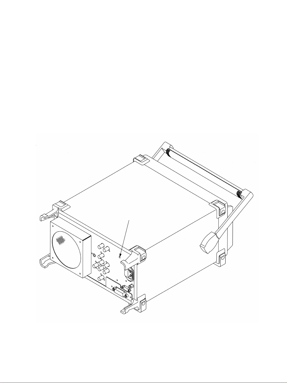
(3) Adjust the “Reference Adjust Screw (Multi-turn potentiometer)” visible through the hole provided on the rear panel
(refer to Fig. 2-2-2) to make the MF76A reading 1,000,000,000 Hz ±5 Hz.
Reference Adjust Screw
Fig. 2-2-2 The location of an adjuster of Reference crystal oscillator
2-17
Page 26
Section 2 MS2665C
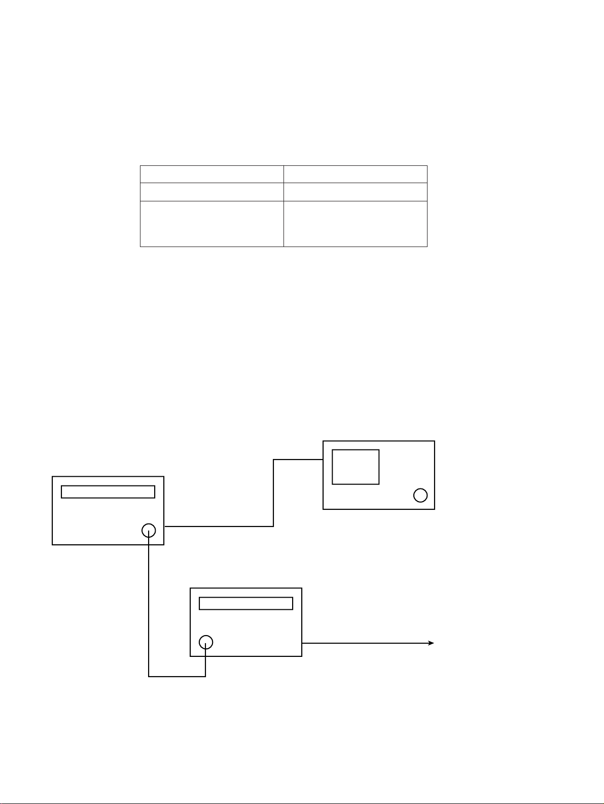
2.2.5.2 Sweep adjustment
Required equipment :
(1) 6769B Swept frequency synthesizer,
(2) MG3633A Synthesized signal generator,
(3) HP3478A Digital multimeter.
Setup for the procedure (1), (2) :
MG3633A
Output
Fig. 2-2-3
Connect the spectrum analyzer RF Input to MG3633A OUTPUT.
Setup for the procedure (3) :
(1) Connect digital multimeter HI input to the TP4 terminal on A1306 MICRO DRIVER PC board attached to A13
MICRO CONVERTER.
(2) Connect digital multimeter LO input to the spectrum analyzer’s common.
Setup for the procedure (4), (5), (6) :
The spectrum analyzer
RF Input
6769B
RF Output
Fig. 2-2-4
(1) Connect the spectrum analyzer RF Input to 6769B RF OUTPUT.
The spectrum analyzer
2-18
RF Input
Page 27

Procedure :
(1) Local sweep adjustment
Initialize the spectrum analyzer and the MG3633A.
1) Set the spectrum analyzer to :
Center frequency, 100 MHz
Span, 100 kHz
Set the MG3633A output to :
LEVEL, -10 dBm
Frequency, 100 MHz (CW)
Press “→CF” key of the spectrum analyzer.
2) Set the MG3633A output frequency to 99.96 MHz (CW).
On the spectrum analyzer, press “Peak Search” key, and set the marker function to delta maker mode (Press
“Marker” key and press “F2” key).
3) Set the MG3633A output frequency to 100.04 MHz (CW).
On the spectrum analyzer, press “Peak Search” key, and read the frequency difference between 99.96 MHz input
and 100.04 MHz input.
2.2 Troubleshooting
4) Adjust the variable resistor R96 on A08 LOCAL-A (refer to Fig. 2-2-5) until the reading of frequency difference
becomes 80 kHz ±200 Hz, to repeat the procedure 2), 3).
(2) YTO FM sweep adjustment
Initialize the spectrum analyzer.
1) Set the spectrum analyzer to :
Center frequency, 1000 MHz
Span, 10 MHz
Set the MG3633A output to :
Frequency, 1000 MHz (CW)
Press “→CF” key of the spectrum analyzer.
2) Set the MG3633A output frequency to 996 MHz (CW).
On the spectrum analyzer, press “Peak Search” key, and set the marker function to delta maker mode (Press
“Marker” key and press “F2” key).
3) Set the MG3633A output frequency to 1004 MHz (CW).
On the spectrum analyzer, press “Peak Search” key, and read the frequency difference between 996 MHz input
and 1004 MHz input.
4) Adjust the variable resistor R53 on 3GHz CONVERTER (refer to Fig. 2-2-5) until the reading of frequency
difference becomes 8 MHz ±40 kHz, to repeat the procedure 2), 3).
2-19
Page 28

Section 2 MS2665C
(3) YTF tuning DAC adjustment
1) Turn the spectrum analyzer on, while pushing “0” key, and initialize the spectrum analyzer.
2) Set the spectrum analyzer to zero Span.
3) Enter Cal menu by pushing “Shift + 0” keys. Open the second page of the Cal menu, and enter Maintenance menu
with “F6” key. Enter RF/Micro converter maintenance menu with “F2” key, and open the 6th page of the menu
(Press “More” key 5 times).
4) Set YTF Pre-tuning value to 3600 by pushing “F2” key (assigned YTF Pre-tuning function) and data keys.
5) Adjust the variable resistor R60 on the A13 MICRO CONVERTER (refer to Fig. 2-2-6) to make multimeter
reading -3.600 ±0.005 Volts.
6) Set YTF Pre-tuning value to 7600 by pushing “F2” key.
7) Adjust the variable resistor R57 on the A13 MICRO CONVERTER (refer to Fig. 2-2-6) to make multimeter
reading -7.600 ±0.005 Volts.
8) Repeat the procedure 4), 5), 6), 7) until you get the required voltage corresponding to each YTF Pre-tuning value.
(4) YTF tuning adjustment
1) Initialize the spectrum analyzer (Press “Preset” key and press “F1” key).
2) After 5 seconds waiting, set the spectrum analyzer to :
Center frequency, 2.92 GHz
Zero Span
Set the 6769B output to :
Frequency, 2.92 GHz (CW)
RF LEVEL, -20 dBm
3) Enter Cal menu by pushing “Shift + 0” keys. Enter Pre-selector Tuning menu with “F6” key.
4) Press “F2” key and set Pre-selector bias value to 0, using the data keys or the knob on the front panel.
5) Adjust the variable resistor R22 on A13 MICRO CONVERTER (refer to Fig. 2-2-6) to make displayed signal
level maximum.
6) Set the spectrum analyzer to :
Center frequency, 6.4 GHz
Zero Span
Set the 6769B output to :
Frequency, 6.4 GHz (CW)
RF LEVEL, -20 dBm
2-20
Page 29

2.2 Troubleshooting
7) Enter Cal menu by pushing “Shift + 0” keys. Enter Pre-selector Tuning menu with “F6” key.
8) Press “F2” key and set Pre-selector bias value to 0, using the data keys or the knob on the front panel.
9) Adjust the variable resistor R31 on A13 MICRO CONVERTER (refer to Fig. 2-2-6) to make displayed signal
level maximum.
10) Put the screw of the variable resistor R68 on A13 MICRO CONVERTER (refer to Fig. 2-2-6) center in its rotation
range.
(5) YTO main sweep adjustment
Initialize the spectrum analyzer and the 6769B.
1) Set the spectrum analyzer to :
Center frequency, 1.5 GHz
Span, 3 GHz
Set the 6769B output to :
RF LEVEL, -10 dBm
Frequency, 1.5 GHz (CW)
Press “→CF” key of the spectrum analyzer.
2) Set the 6769B output frequency to 300 MHz.
On the spectrum analyzer, press “Peak Search” key, and set the marker function to delta marker mode (Press
“Marker” key and press “F2” key).
3) Set the 6769B output frequency to 2.7 GHz.
On the spectrum analyzer, press “Peak Search” key, and read the frequency difference between 300 MHz input
and 2.7 GHz input.
4) Adjust the variable resistor R57 on 3GHz CONVERTER (refer to Fig. 2-2-5) until the reading of frequency
difference becomes 2.4 GHz ±6 MHz, to repeat the procedure 2), 3).
5) Initialize the spectrum analyzer (Press “Preset” key and press “F1” key).
Set the 6769B to :
Frequency, 14.2 GHz (CW)
RF LEVEL, -20 dBm
6) Set Pre-selector bias value to 0, according to above-mentioned procedure.
7) Press “Peak Search” key to place marker indicator on the top of 14.2 GHz signal.
8) Adjust the variable resistors R63 and R64 on A13 MICRO CONVERTER (refer to Fig. 2-2-6) to make the signal
level maximum, i.e. increase the level roughly with R63, and then using R64, make it exactly maximum.
2-21
Page 30

Section 2 MS2665C
(6) Confirmation of YTF tuning
Initialize the spectrum analyzer and the 6769B.
1) Set the spectrum analyzer to :
Start frequency, 3 GHz
Stop frequency, 21 GHz
Log Scale, 2 dB
Storage Max Hold (Press “A, B” key, press “F5” key and “F2” key).
2) Set the 6769B to :
F1 frequency, 3 GHz
F2 frequency, 21 GHz
RF LEVEL, -10 dBm
Analog sweep ON
Sweep time, 50 seconds
3) Confirm that the waveform on the analyzer’s display is flat, after the 6769B finishes its 50-second sweeping.
R53, R57
R96
Fig. 2-2-5 The location of adjusters on A08 LOCAL-A and 3GHz CONVERTER
2-22
Page 31

R22, R31, R57, R60, R68
Jumper pin X12
2.2 Troubleshooting
Fig. 2-2-6 The location of adjusters on A13 MICRO CONVERTER
2-23
Page 32

Section 2 MS2665C
2.2.5.3 IF1 (ATT), IF2 (AMP) adjustment
Required equipment :
(1) 6769B swept frequency synthesizer
(2) ML4803A Power meter
(3) MA4705A Power sensor
(4) IBM PC/AT compatible
Setup :
(1) Connect the spectrum analyzer RF Input to 6769B RF OUTPUT
(2) Connect the spectrum analyzer and the personal computer with RS-232C interface
Procedure :
(1) Turn the spectrum analyzer on, while pushing “0” key.
(2) Initialize the spectrum analyzer :
1) Enter Preset menu with “Preset” key,
2) Initialize the spectrum analyzer completely with “F1” key.
(3) Calibrate the spectrum analyzer using its internal calibration function :
1) Enter Cal menu with “Shift” key and “0” key,
2) Calibrate the spectrum analyzer by pushing “F1” key.
[ Mixer harmonic order 1 ]
(4) Set mixing mode to Band 1- :
1) Enter Frequency menu by pressing “Frequency” key, and open its second page with “More” key,
2) Enter Band menu with “F1” key,
3) Set mixing mode to Band 1- by pushing “F3” key.
(5) Set the spectrum analyzer to :
Center frequency, 5.00 GHz
Span, 1 MHz
Set the 6769B output frequency to 5.00 GHz (CW).
(6) Adjust the 6769B output level to make power meter reading -10 dBm at the end of cable feeding the signal to the
spectrum analyzer, and then connect the cable to the spectrum analyzer’s RF Input.
(7) Tune the spectrum analyzer’s pre-selector, using its pre-selector auto tune function :
1) Enter Cal menu with “Shift + 0” key,
2) Enter Pre-selector Tuning menu with “F6” key,
3) Tune the pre-selector by pushing “F1” key.
(8) Read marker level using peak search function (Press “Peak Search” key), and if maker reading is within -10 dBm ±0.2
dB, skip next procedure.
2-24
Page 33

2.2 Troubleshooting
(9) Enter RF/MICRO CONVERTER maintenance menu, and open its 6th page :
1) Enter Cal menu by pushing “Shift + 0” key. Open the second page of the Cal menu,
2) Enter maintenance menu with “F6” key,
3) Enter RF/Micro Converter maintenance menu with “F2” key. Open the 6th page of the RF/Micro Converter
maintenance menu (Press “More” key 5 times).
Adjust IF-Gain 1 and IF-Gain 2 so that the maker reading becomes -10 dBm ±0.2 dB.
[ Mixer harmonic order 2 ]
(10) Set mixing mode to Band 2+ (refer to the procedure (4)).
(11) Set the spectrum analyzer to :
Center frequency, 12.01 GHz
Span, 1 MHz
Set the 6769B output frequency to 12.01 GHz (CW).
(12) Adjust the 6769B output level to make power meter reading -10 dBm at the end of cable, and then connect the cable
to the spectrum analyzer’s RF Input.
(13) Tune the spectrum analyzer’s pre-selector (refer to the procedure (7)).
(14) Read marker level with “Peak Search” key, and if marker reading is not within -10 dBm ±0.2 dB, adjust IF-Gain 1 and
2 to make the reading -10 dBm ±0.2 dB (refer to the procedure (9)).
[ Mixer harmonic order 3 ]
(15) Set mixing mode to Band 3+ (refer to the procedure (4)).
(16) Set the spectrum analyzer to :
Center frequency, 18.201 GHz
Span, 1 MHz
Set the 6769B output frequency to 18.201 GHz.
(17) Adjust the 6769B output level to make -10 dBm with power meter at the end of cable, and then connect the cable to the
spectrum analyzer’s RF Input.
(18) Tune the spectrum analyzer’s pre-selector (refer to the procedure (7)).
(19) Read the marker level with “Peak Search” key, and if marker reading is not within -10 dBm ±0.2 dB, adjust IF-Gain
1 and 2 to make the reading -10 dBm ±0.2 dB (refer to the procedure (9)).
2-25
Page 34

Section 2 MS2665C
(20) Write the compensation value of adjusted IF-Gain 1 and IF-Gain 2 to the spectrum analyzer’s Flash Memory with
Flash Memory writing command “CDW” from personal computer. For example :
CMD > MENTE P2110 ON
CMD > CD40 1, 0
CMD > CD41 1, 3
CMD > CD40 2, 0
CMD > CD41 2, 17
CMD > CD40 3, 0
CMD > CD41 3, 30
CMD > CDW
, where
line 1 makes the spectrum analyzer maintenance mode ON.
<CD40 n, m> is IF-Gain 1 setting statement. “n” is a mixer harmonic order number. “m” is a compensation value in
procedure (9), (14), (19) (0 to 255 integer).
Similarly, <CD41 n, l> is IF-Gain 2 setting statement. “l” is the compensation value (0 to 255 integer).
2.2.6 Assembling cabinet
Refer to 2.3.1.
2.2.7 Checking items after assembling cabinet
After switching the power on, check for the following faults.
(1) No burning smell and/or smoke.
(2) Fan rotates
(3) No strange sounds.
After checking the above items, make sure the original defect has been repaired.
2-26
Page 35

2.2 Troubleshooting
2.2.8 Frequency response compensation
Perform Frequency response compensation, when one of the following modules is replaced. This Frequency response
compensation is not necessary, if the module you replaced does not belong to the following modules.
• A03 CPU • 21GHz S-ATT
• 3GHz CONVERTER • 21GHz YTF/SW
• A13 MICRO CONVERTER • H. MIXER
• A14 1st LO AMP
Frequency response caused by front-end components such as step attenuator, low pass filter and mixer is corrected by
measuring the response and storing the data in instrument’s memory.
Frequency response compensation process consists of four steps that are performed semi-automatically with “Frequency
Response Compensation” software. The four steps are as follows :
1. DUT (Device Under Test) check,
2. Signal source power output calibration with power meter,
3. Frequency response measurement using the calibrated power output,
4. Compensation data updating.
Required instrument :
(1) 6769B Swept Frequency Synthesizer
(2) MG3633A Synthesized Signal Generator
(3) two ML4803A Power Meters
(4) MA4705A Power Sensor
(5) MA4601A Power Sensor
(6) two 3 dB attenuators
(7) IBM-PC/AT compatible for controller
(8) GPIB-PC2/2A
(9) ML2437A Power Meter (for MS2667C and MS2668C)
(10) MA2444A Power Meter (for MS2667C and MS2668C)
Required software :
(1) MS-DOS Ver. 5.0 or later and Windows 3.1, or Windows 95
(2) Frequency Response Compensation software.
2-27
Page 36

Section 2 MS2665C
Setup :
IBM-PC/AT Compatible
GP-IB control
The spectrum analyzer
6769B
3 dB
attenuator
MG3633A
RF Output
RF Input
Power meter :
ML4803A (for MS2665C)
ML2437A (for MS2667/68C)
3 dB
attenuator
Power sensor :
MA4705A (for MS2665C)
MA2444A (for MS2667/68C)
OUTPUT
ML4803A
2-28
Power sensor : MA4601A
Fig. 2-2-7
Page 37

2.2 Troubleshooting
(1) At the measurement of frequency response, connect the spectrum analyzer’s RF Input to 6769B RF OUTPUT through
a signal feeder. The signal feeder consists of a coaxial cable (e.g. SUCOFLEX) less than 1 m length and two 3 dB
attenuators attached to each end of the cable.
(2) At the calibration of power output, connect the end of the feeder to power sensor.
Note that 1) the coaxial cable and 3 dB attenuators must be with a frequency range over the spectrum analyzer’s range,
2) use a torque wrench for tightening each connection, 3) do not disconnect the connections of the 6769B and the
signal feeder after the power calibration in order to keep the measured data valid.
Procedure :
Note that the spectrum analyzer (DUT) and the measuring instruments must be warmed up at least for an hour, before the
compensation process.
(1) Run the Frequency Response Compensation program, and then confirm that 6769B output is set to 10 MHz (CW).
(2) After 5 minutes waiting or more, input the serial number of the spectrum analyzer to the personal computer.
(3) Execute “DUT Check” by pushing the button on the PC display.
(4) After internal calibration of the spectrum analyzer, confirm that the spectrum analyzer’s “Cal Status” is all zero.
(5) Carry out zero adjustment and sensor sensitivity adjustment on the power meter, and then connect the MA4601A
power sensor to the end of the cable from MG3633A OUTPUT.
(6) Set MG3633A output to 625 kHz (CW), and adjust the output level so that power meter reading becomes 0 dBm at the
end of the cable, and then connect this end to the spectrum analyzer RF Input.
(7) After “Preset All”, set the spectrum analyzer to :
Center frequency, 625 kHz
Span, 50 kHz
RBW, 10 kHz
VBW, 1 kHz
Atten, 10 dB
Reference Level, 0 dBm
(8) On the spectrum analyzer’s display, read the marker level of 625 kHz signal, and input the reading to “625 kHz CAL
OSC Level” space on the PC display. For example: when marker reading is 0.30 dBm, input “0.30” to the space.
2-29
Page 38

Section 2 MS2665C
(9) Measure the 6769B power output with “6769B output calibration” program.
1) Connect the 6769B RF OUTPUT to the MA4601A (for MS2665C) or MA2444A (for MS2667/68C) through a
signal feeder. The signal feeder consists of a coaxial cable (e.g. SUCOFLEX) less than 1 m length and two 3 dB
attenuators attached to each end of the cable. Note : Use a torque wrench for tightening each connection.
2) Run the “6769B output calibration” program by pushing the button on the PC display.
3) Change the power sensor for the MA4705A according to PC message. (for MS2665C only)
4) Before going to next step, leave the 6769B at least for 5 minutes after the program stopping.
Note that 1) The connections of the 6769B and the signal feeder must not be disconnected after the measurement
in order to keep the measured data valid, 2) this measurement is needed once a day, as long as the 6769B is power
on.
(10) Connect the end of the signal feeder to the spectrum analyzer RF Input.
(11) Run “Frequency Response Measurement” program with the button on the PC display.
(12) Write frequency response compensation data into the spectrum analyzer’s memory with the button on the PC display.
2-30
Page 39

2.3 Mechanical configuration
2.3.1 Disassembling/Assembling cabinet
(1) Removing Feet (1 to 8)
Remove the S1/S2/S3 screws and remove the S3 screw of the rear.
(2) Removing around cover
Remove the four S1 screws (1 to 4) and remove the S3 screw of the rear.
Remove the around cover 10 to pull backward.
(3) Removing Front Frame
After (1) removing procedure, remove the 11 to pull forward.
To assemble, perform inversely.
Parts List
1
32E11805A Front foot
2
32E11805B Front foot
3
32E11806A Front foot Receiver
4
32E11806B Front foot Receiver
5
32E11807A Rear foot
6
32E11807B Rear foot
7
32E11808A Rear foot Receiver
8
32E11808B Rear foot Receiver
9
34Y107601 Tilt handle 3/4MW
10
333B35279 Around cover assembly
11
32E13058 Front frame
10
11
2.3 Mechanical configuration
2-31
Page 40

Section 2 MS2665C
2-32
Page 41

2.3 Mechanical configuration
Fig. 2-3-1
2-33
Page 42

Section 2 MS2665C
2-34
Page 43

2.3.2 Removing/Assembling units and PC boards
2.3 Mechanical configuration
(1) Removing MICRO CONVERTER 4 and 1ST LO AMP
5
After removing the screws and each cables, remove the 4 5 to pull backward.
(2) Removing Step Attenuator 3 Band ATT Angle
2
After removing the S1/S2 screws, remove the 2 3.
(3) Removing 21 GHz YTF/SW
After removing the Angle 8, remove the
(4) Removing PMC/GPIB 18 and CPU board
7
7
17
After removing the S3 screw, remove the 17 18 to pull backward.
To assemble, perform inversely.
Parts List
1
34J107713 N-J SMA-P Adapter
2
332B36744B ATT Angle
3
339H37752 21GHz Step Attenuator
4
34Y110446C A13 MICRO CONVERTER
5
34Y110447 A14 1ST LO AMP
6
329H13290 H.MIXER
7
329H13289 21GHz YTF/SW
8
34B111361 Angle
9
33B38019 Plate
10
34J110924 Semi-rigid cable
11
439H32078 SMA-Attenuator
12
34J117955 Semi-rigid cable
13
33J41281 Semi-rigid cable
14
33J41282 Semi-rigid cable
15
34J110713 Semi-rigid cable
16
34J117700 Semi-rigid cable
17
34Y106690 A03 CPU
18
34Y106693 A04 PMC/GPIB
or 34Y106692B or A04 PMC/CENTRONICS
2-35
Page 44

Section 2 MS2665C
2-36
Page 45

2.3 Mechanical configuration
Fig. 2-3-2
2-37
Page 46

Section 2 MS2665C
5
15
4
S2
2
10
7
13
11
6
12
18
9
16
17
1
S1
S3
2-38
Fig. 2-3-3
Page 47

2.3.3 Front unit disassembly/assembly
Removing TFT LCD MODULE
(1) After removing the S1, S2 screws and encoder knob 5, remove the front panel 1.
(2) After removing the S3 screw, remove the 2, 3 and 4 to pull forward.
(3) After removing the S4 screw and each cables, remove the LCD 2.
To assemble, perform inversely.
Parts List
1
322B13049 Front panel
2
No1256 TFT LCD MODULE
3
332B40222 LCD panel
4
322B13048 Front cover
5
33E32858 Encoder knob
6
34Y106676 A02 FRONT BOARD
7
34Y106673 A01 MOTHER BOARD
2.3 Mechanical configuration
2-39
Page 48

Section 2 MS2665C
2-40
Page 49

S1
2.3 Mechanical configuration
7
4
S4
3
S3
2
1
6
5
S2
Fig. 2-3-4
2-41
Page 50

Section 2 MS2665C
2-42
Page 51

2.3.4 A09 OPTION BASE disassembly/assembly
Parts List
1
34Y106684 A09 OPTION BASE
2
34Y106695 A0901 TRIG/GATE
3
34Y106699 A0902 AM/FM MONITOR
4
34Y106697 A0903 TV MONITOR
5
34Y113473 A0904 QP DETECTOR
or 34Y117105
2.3 Mechanical configuration
2-43
Page 52

Section 2 MS2665C
2-44
Page 53

2.3 Mechanical configuration
3
2
4
1
5
Fig. 2-3-5
2-45
Page 54

Section 2 MS2665C
2-46
Page 55

2.3 Mechanical configuration
2.3.5 Removing/Assembling A0501 HI-SPEED AD from A05 SCAN/AD
Parts List
1
34Y112923A A05 SCAN/AD
or 34Y112923C
2
34Y106688 A0501 HI-SPEED AD
2
1
Fig. 2-3-6
2-47
Page 56

Section 2 MS2665C
2-48
.
Page 57

Section 3 MS2667C
3.1 Overall Circuit description ......................................................... 3-2
3.2 Troubleshooting......................................................................... 3-9
3.2.1 Introduction .................................................................... 3-9
3.2.1.1 Service kit ......................................................... 3-9
3.2.1.2 Required equipment ......................................... 3-9
3.2.1.3 Circuit reference ............................................... 3-10
3.2.2 Detecting faulty module ................................................. 3-15
3.2.3 Disassembling cabinet................................................... 3-16
3.2.4 Replacement of faulty module ....................................... 3-16
3.2.5 Adjustment after module replacement ........................... 3-16
3.2.5.1 Reference crystal oscillator adjustment .......... 3-16
3.2.5.2 Sweep adjustment .......................................... 3-16
3.2.5.3 IF Gain-1 (ATT), IF Gain-2 (AMP) of Internal
Mixer Band adjustment.................................... 3-26
3.2.5.4 IF Gain-1 (ATT), IF Gain-2 (AMP) of External
Mixer Band adjustment.................................... 3-30
3.2.6 Assembling cabinet........................................................ 3-32
3.2.7 Checking items after assembling cabinet ...................... 3-32
3.2.8 Frequency response compensation .............................. 3-32
3.3 Mechanical configuration........................................................... 3-33
3.3.1 Disassembling/Assembling cabinet ............................... 3-33
3.3.2 Removing/Assembling units and PC boards ................. 3-37
3.3.3
3.3.4 Disassembling/Assembling Units and Components on
3.3.5 Front unit disassembly/assembly................................... 3-51
3.3.6 OPTION BASE disassembly/assembly ......................... 3-55
3.3.7 Removing/Assembling A0501 HI-SPEED AD
3.3.8 Connecting the cable to Diplexing Bandswitch
Disassembling/Assembling Components around RF Input .....
lower surface ................................................................. 3-45
from SCAN/AD............................................................... 3-59
and F2626 (YTF) ........................................................... 3-60
3-41
3-1
Page 58

Section 3 MS2667C
3.1 Overall Circuit description
MS2667C is a superheterodyne system scanning-type spectrum analyzer.
This section describes overall circuit of the MS2667C spectrum analyzer with its block diagram.
An RF input signal after passing through an RF switch and variable RF ATTN in Switched Attenuator is switched by
Diplexing Bandswitch to two different signal routes depending on input RF frequency.
For an RF input frequency of 9 kHz to 3.1 GHz (termed as band 0), the signal passes through 3.2 GHz LPF and then to 1st
mixer (1st MIX), where it is mixed with 1st local signal (4.1 GHz to 7.2 GHz) to generate 4110.69 MHz 1st IF signal.
The 1st IF signal is then passed through an amplifier and image rejection filters, and fed to 2nd mixer (2nd MIX), where it
is mixed with 4 GHz 2nd local signal to generate 110.690 MHz 2nd IF signal.
For an RF input frequency of 3.1 GHz to 30 GHz (band 1 to 5), the signal goes to YTF (YIG tuned filter), and then to 30
GHz H.MIXER. In 30 GHz H.MIXER, the RF signal gets mixed with the 1st local signal (3.6 GHz to 7.5 GHz) to generate
689.31 MHz 1st IF signal.
This 1st IF signal is passed through a series of amplifiers and image rejection filters before further mixing with 800 MHz
2nd local signal to convert the signal to the 110.690 MHz 2nd IF signal.
Depending on the active band of RF input, one of the two above 2nd IF signal is sent to IF section for further processing.
The 1st local signal generated at YTO (YIG tuned oscillator) is frequency-swept by scan signal from SCAN/AD section
after phase-lock to reference signal (its frequency is 11 MHz to 14 MHz with the resolution of 1 Hz steps) generated on
LOCAL-SP1, 2 section at the center frequency of its sweeping range, in normal sweep condition.
The YTO output is passed through an amplifier, and then divided into three paths with directional couplers. One of divided
signal is fed to sampler circuit and the other are fed to the above mixers to frequency-convert.
In the sampler circuit, sampling signal (its frequency is 94 MHz to 106 MHz with the resolution of 1 MHz steps) generated
on LOCAL-SP1, 2 section is frequency-multiplied, and then mixed with the YTO output to generate sampler IF signal with
a frequency of 11 MHz to 14 MHz.
The sampler IF signal is compared with the reference signal of 11 MHz to 14 MHz at PFD.
The reference signal frequency (fREF) and the sampling signal frequency (fs) are controlled by CPU section according to
the measuring frequency of the instrument, and set so that the center frequency of 1st local signal is fs * N ± fREF (, where
N is an integer).
Meanwhile, the scan signal strength that is equivalent to frequency sweep width is controlled from LOCAL-SP1, 2 section.
The 2nd local signals of 4 GHz and 800 MHz are also phase-locked to 100 MHz VCXO signal, of which the frequency is
also phase-locked to 10 MHz crystal oscillator.
In the instrument, a high accuracy 625 kHz signal is present for level accuracy calibration. This signal is generated by
frequency-dividing the 10 MHz reference signal, and its power level is varied with 1 dB steps by CAL ATT.
Internal calibration operation being carried out, this calibrating signal is fed to the RF signal-route through the switch in
Switched Attenuator.
3-2
Page 59

3.1 Overall Circuit description
At the IF section the incoming signal is divided into two paths. The main route leads to image rejection filters while the
second, a highly attenuated feeler path signal is used for generation of wide band trigger signal in TRIG/GATE section
(option 06) situated on OPTION BASE board.
The main signal after passing through an image rejection filter is beat down to a 10.69 MHz signal using a 100 MHz
reference signal. This signal is then sent to various Resolution Band Width (RBW) setting circuits.
For RBW setting of 30 Hz to 200 Hz the signal is frequency converted to 450 kHz using 10.24 MHz signal. After passing
through the RBW circuits (Crystal filter circuits) the signal is up converted back to 10.690 MHz signal and passed through
wider RBW setting circuits. For RBW setting of 300 Hz to 3 MHz the signal is sent directly to wide RBW setting circuits
without any frequency modifications.
The RBW processed signal is passed onto SCAN/AD section, where it passes through logarithmic amplifiers and then to a
linear detector. This linear detected signal is passed through smoothing filters called Video Band Width Filters (VBW).
This smoothed signal is then passed through Positive or Negative peak detection circuits and the output is converted to
digital signal by a Analog to Digital Converter (ADC) circuit.
The results are then written (in digital word format) to a Dual Port RAM through one of the ports.
The CPU of the instrument on CPU section reads from the other port of Dual Port RAM and processes the data before
displaying on the LCD screen. The CPU also controls various interface functions such as reading the Key Inputs or remote
control commands received, and various outputs such as prints or plots of various data. The CPU also generates various
commands required for controlling or setting of all hardware units inside the instrument.
FRONT BOARD section generates the KEY and rotary-knob encoder data, drives the LEDs, detects the power switch
(PWR SW) setting, controls the power-supply On/Stby setting, and supplies power for the LCD backlight, etc.
3-3
Page 60

Section 3 MS2667C
3-4
Page 61

3.1 Overall Circuit description
3-5
Page 62

Section 3 MS2667C
3-6
Page 63

3.1 Overall Circuit description
3-7
Page 64

Section 3 MS2667C
3-8
Page 65

3.2 Troubleshooting
3.2.1 Introduction
This section describes how to troubleshoot the MS2667C.
3.2.1.1 Service kit
Refer to 2.2.1.1.
3.2.1.2 Required equipment
Table 3-2-1 shows the equipment to prepare for overall adjustment of the spectrum analyzer.
Table 3-2-1 Required equipment
3.2 Troubleshooting
Synthesized signal generator
Frequency counter
Swept frequency synthesizer
Power meter
Power sensor
Power meter
Power sensor
Adapter (K female to K female)
Digital multimeter
GPIB interface board
two 3 dB attenuators
IBM-PC/AT compatible
a printer
Model number
MG3633A
MF76A
6769B
ML4803A
MA4601A
ML2437A
MA2444A
K222B
HP3478A
GPIB-PC2/2A
41KC-3
ManufactureNomenclature
Anritsu
Anritsu
Anritsu
Anritsu
Anritsu
Anritsu
Anritsu
Anritsu
Hewlett Packard
National Instruments Corp.
Anritsu
3-9
Page 66

Section 3 MS2667C
3.2.1.3 Circuit reference
This paragraph supplies the exchange module list of the spectrum analyzer with its overall circuit diagram.
Table 3-2-2 Exchange Modules of MS2667C
Schematic number Name Model name
10
11
12
13
14
15
16
17
18
1
2
3
4
5
6
7
8
9
MOTHER BOARD
A02 FRONT BOARD
A03 CPU
A04 PMC/GPIB
SCAN/AD
IF(B)
LOCAL-SP2
LOCAL-SP1
RF CONVERTER
2nd CONVERTER
1ST LO AMP
AK-AKF PANEL CONNECTOR
Switched Attenuator
Diplexing Bandswitch
OPEN LOOP YIG FILTER
30GHz YTF
30GHz H.MIXER
POWER SUPPLY UNIT
TFT LCD MODULE
OPTION BASE
MM200013A
322U14223
322U14225
322U12853
MM200014A
MM200015A
MM200016A
MM200017A
MM200019A
MM200020A
MM200022B
MM200021A
B46790
D29638
D29870
F2626
MM200001A
339H41184B
34Z114508
NL3224AC35-01
MM200018A
Ordering number
34Y115415
34Y118357
34Y118358
34Y106693
34Y112923D
34Y106718B
34Y111112B
34Y111111B
34Y117226
34Y117228
34Y117228B
34Y118007
B46790
D29638
D29870
34Y117225
339H41853
339H41184B
34Z114508
No1256
34Y106684B
Note
Order both
numbers
*pair 1
*pair 2
*pair 1
*pair 2
Options
19
20
21
22
To identify a exchange module, a label printed “Model number” is pasted on module.
Remark :
1. MS2667C has two kinds of YTF as exchange module. When you replace a YTF, check YTF model according to
following procedure.
(1) Keep key “0” depressed while switching on the spectrum analyzer.
(2) Enter RF/Micro Conv maintenance menu.
1) Enter Cal menu by pushing “Shift” + “0” keys. Open second page of Cal menu by pushing “more”.
2) Enter maintenance menu with “F6” (Maintenance) key.
(3) Press “F1” (Version & options) keys.
A0501 HI-SPEED AD
A0901 TRIG/GATE
A0902 AM/FM MONITORA
A04 PMC/CENTRONICS
332U36333
34Y106695B
34Y106699B
34Y106692B
34Y106688
34Y106695B
34Y106699B
34Y106692B
Option 04
Option 06
Option 07
Option 10
3-10
Page 67

3.2 Troubleshooting
(4) Press Key “more” 3 times. MAINTENANCE (4/4) page appears. Check YTF model. If “09 : YTF MODEL” is
not indicated, order “F2626”.
If “09 : YTF MODEL” is indicated, order same model which is indicated.
YTF Model
2. 2nd Converter (Schematic number 9) and YTF (Schematic number 14) forms a pair.
*pair 1 : MM200020A (34Y117228) and F2626 (34Y117225)
*pair 2 : MM200022B (34Y117228B) and MM200001A (339H41853)
When you replace a YTF, make sure to order the same model number.
When you replace 2nd Converter, Check model number of YTF (easily visible) and make sure to order it’s matching
pair.
3. When you replace a A02 FRONT BOARD or A03 CPU, check circuit board number (322U******) of A03 CPU.
If circuit board number of A03 CPU is 322U13903, make sure to order A02 FRONT BOARD (322U14223) and A03
CPU (322U14225).
If circuit board number of A03 CPU is 322U14225, make sure to order one module which you replace.
3-11
Page 68

Section 3 MS2667C
3-12
Page 69

3.2 Troubleshooting
13
10
14
15
12
11
12
13
14
15
8
1
9
7
7
10
3-13
Page 70

Section 3 MS2667C
17
19
20
18
16
21
2
17
6
18
20
21
19
5
16
3
4
3-14
Page 71

3.2.2 Detecting faulty module
The flowchart shows the way to locate the faulty module among them.
3.2 Troubleshooting
POWER ON
LEDs come on?
The LCD comes on?
Fan Movement?
Key, Rotary knob come on?
Sweeping?
Trace Displayd When signal input?
Freq Display correct?
Level Display correct?
RBW Setting?
VBW Setting?
No
No
No
No
No
No
No
No
No
No
[Location of faulty module]
Fuse, A02 FRONT BOARD, POWER SUPPLY UNIT
A03 CPU, TFT LCD MODULE, POWER SUPPLY UNIT
POWER SUPPLY UNIT
A02 FRONT BOARD, A03 CPU
SCAN/AD, LOCAL-SP2, LOCAL-SP1, A03 CPU
RF CONVERTER, 2nd CONVERTER,
Switched Attenuator, Diplexing Bandswitch, YTF, 30GHz H.MIXER
LOCAL-SP2, LOCAL-SP1, RF CONVERTER
RF CONVERTER, IF, 2nd CONVERTER,
Switched Attenuator, Diplexing Bandswitch, YTF, 30GHz H.MIXER
IF
SCAN/AD
Input A TT Setting?
LOG/LIN Setting?
TRIG Setting?
Det mode Setting?
Display mode Setting?
Hardcopy possible?
Memory Backup?
(Yes)
Normal
No
No
No
No
No
No
No
RF CONVERTER, Switched Attenuator
SCAN/AD
A0902 TRIG/GA TE
SCAN/AD
A03 CPU
A03 CPU
A03 CPU
3-15
Page 72

Section 3 MS2667C
3.2.3 Disassembling cabinet
Refer to 3.3.1.
3.2.4 Replacement of faulty module
Refer to 3.3.2 to 3.3.8.
3.2.5 Adjustment after module replacement
This paragraph describes the overall adjustment required after replacement of any modules in following Table. Look for
modules which you replaced in Table. Please carry out work corresponding to module which you replaced. This adjustment is not necessary, if the module you replaced does not belong to the following Table.
Replaced module
LOCAL-SP2 and LOCAL-SP1 Carry out 3.2.5.1 and 3.2.5.2.
RF CONVERTER Carry out 3.2.5.2 and 3.2.5.3.
OPEN LOOP YIG FILTER (F2626)
30GHz YTF
2nd CONVERTER Carry out 3.2.5.2 to 3.2.5.4.
30GHz H.MIXER Carry out 3.2.5.3.
A03 CPU Carry out 3.2.5.3 and 3.2.5.4.
3.2.5.1 Reference crystal oscillator adjustment
Refer to 2.2.5.1.
3.2.5.2 Sweep adjustment
Required equipment :
(1) 6769B Swept frequency synthesizer
(2) MG3633A Synthesized signal generator
(3) HP3478A Digital multimeter
3-16
Page 73

Setup for the procedure (1), (2) :
3.2 Troubleshooting
MG3633A
Output
Fig. 3-2-1
Connect the spectrum analyzer RF Input to MG3633A OUTPUT.
Setup for the procedure (3) :
(1) Connect digital multimeter HI input to the X3 terminal on LOCAL-SP2 PC board. (Refer to Fig. 3-2-4)
(2) Connect digital multimeter LO input to the spectrum analyzer’s common.
Setup for the procedure (4) :
(1) Connect digital multimeter HI input to the X21 terminal on LOCAL-SP2 PC board. (Refer to Fig. 3-2-4)
(2) Connect digital multimeter LO input to the spectrum analyzer’s common.
The spectrum analyzer
RF Input
Setup for the procedure (5) :
(1) Connect digital multimeter HI input to the X3 terminal on A1307 YTF DRIVER PC board attached to 2nd CON-
VERTER. (Refer to Fig. 3-2-5)
(2) Connect digital multimeter LO input to the spectrum analyzer’s common.
Setup for the procedure (6), (7) :
(1) Check model of YTF on lower surface.
(2) Set jumper pins, X10 and X12 on A1307 YTF DRIVER PC board attached to 2nd CONVERTER, to YTF model side
which you checked at (1). (Refer to Fig. 3-2-5 )
Example : When YTF model is “F2626”, jumper pins are set as follows.
F2626
F2626
MM200001A
X10
1313
(X11) (X13)
MLFP1312
(F2726)
MLFP-1312
(F2726)
Jumper pins
X12
MM200001A
Fig.3-2-2
3-17
Page 74

Section 3 MS2667C
(3) Connect the spectrum analyzer RF Input to 6769B RF OUTPUT.
6769B
RF Output
The spectrum analyzer
RF Input
Fig. 3-2-3
3-18
Page 75

Procedure :
(1) Local sweep adjustment
Initialize the spectrum analyzer and the MG3633A.
1) Set the spectrum analyzer to :
Center frequency, 100 MHz
Span, 100 kHz
Set the MG3633A output to :
LEVEL, -10 dBm
Frequency, 100 MHz (CW)
Press “→CF” key of the spectrum analyzer.
2) Set the MG3633A output frequency to 99.96 MHz (CW).
On the spectrum analyzer, press “Peak Search” key, and set the marker function to delta maker mode (Press
“Marker” key and press “F2” key).
3) Set the MG3633A output frequency to 100.04 MHz (CW).
On the spectrum analyzer, press “Peak Search” key, and read the frequency difference between 99.96 MHz input
and 100.04 MHz input.
3.2 Troubleshooting
4) Adjust the variable resistor R123 on LOCAL-SP2 (refer to Fig. 3-2-4) until the reading of frequency difference
becomes 80 kHz ±200 Hz, to repeat the procedure 2), 3).
(2) YTO FM sweep adjustment
Initialize the spectrum analyzer.
1) Set the spectrum analyzer to :
Center frequency, 1000 MHz
Span, 10 MHz
Set the MG3633A output to :
Frequency, 1000 MHz (CW)
Press “→CF” key of the spectrum analyzer.
2) Set the MG3633A output frequency to 996 MHz (CW).
On the spectrum analyzer, press “Peak Search” key, and set the marker function to delta maker mode (Press
“Marker” key and press “F2” key).
3) Set the MG3633A output frequency to 1004 MHz (CW).
On the spectrum analyzer, press “Peak Search” key, and read the frequency difference between 996 MHz input
and 1004 MHz input.
4) Adjust the variable resistor R53 on RF CONVERTER (refer to Fig. 3-2-4) until the reading of frequency difference becomes 8 MHz ±40 kHz, to repeat the procedure 2), 3).
3-19
Page 76

Section 3 MS2667C
(3) YTF offset voltage adjustment 1
1) Set the spectrum analyzer.
Center frequency : 4 GHz
Span : 400 MHz
2) On the spectrum analyzer, press “single” key.
3) After sweep of the spectrum analyzer is finished, check the X3 voltage (multimeter indicated). This voltage value
is V1.
4) Set the spectrum analyzer’s span to 401 MHz.
5) On the spectrum analyzer, press “single” key.
6) After sweep of the spectrum analyzer is finished, check the X3 voltage (multimeter indicated). This voltage value
is V2.
7) Adjust R287 on the LOCAL-SP2 (refer to Fig. 3-2-4) until the difference voltage between V1 and V2 is below ±1
mV, to repeat the procedure 1) to 6).
(4) YTF offset voltage adjustment 2
1) Set the spectrum analyzer.
Center frequency : 4 GHz
Span : 4 GHz
2) On the spectrum analyzer, press “single” key.
3) After sweep of the spectrum analyzer is finished, check the X21 voltage (multimeter indicated). This voltage
value is V1.
4) Set the spectrum analyzer’s span to 4.01 GHz.
5) On the spectrum analyzer, press “single” key.
6) After sweep of the spectrum analyzer is finished, check the X21 voltage (multimeter indicated). This voltage
value is V2.
7) Adjust R280 on the LOCAL-SP2 (refer to Fig. 3-2-4) until the difference voltage between V1 and V2 is below ±1
mV, to repeat the procedure 1) to 6).
3-20
Page 77

3.2 Troubleshooting
R287
X3
X21
R280
R53, R57
R123
Fig. 3-2-4 The location of adjusters on LOCAL-SP2 and RF CONVERTER
3-21
Page 78

Section 3 MS2667C
(5) YTF tuning DAC adjustment
1) Turn the spectrum analyzer on, while pushing “0” key, and initialize the spectrum analyzer.
2) Set the spectrum analyzer to zero Span.
3) Enter Cal menu by pushing “Shift + 0” keys. Open the second page of the Cal menu, and enter Maintenance menu
with “F6” key. Enter RF/Micro converter maintenance menu with “F2” key, and open the 6th page of the menu
(Press “More” key 5 times).
4) Set YTF Pre-tuning value to 3600 by pushing “F2” key (assigned YTF Pre-tuning function) and data keys. (Press
keys “3”+“6”+“0”+“0”+“Enter”)
5) Adjust the variable resistor R27 on the 2nd CONVERTER (refer to Fig. 3-2-5) to make multimeter reading -3.600
±0.005 Volts.
6) Set YTF Pre-tuning value to 7600 by pushing “F2” key. (Press keys “7”+”6”+“0”+“0”+“Enter”)
7) Adjust the variable resistor R30 on the 2nd CONVERTER (refer to Fig. 3-2-5) to make multimeter reading -7.600
±0.005 Volts.
8) Repeat the procedure 4), 5), 6), 7) until you get the required voltage corresponding to each YTF Pre-tuning value.
(6) YTF tuning adjustment
1) Keep key “Preset” depressed while Switching ON the spectrum analyzer.
2) Wait till sweep of the spectrum analyzer starts and after that Switch OFF the power supply of the spectrum
analyzer.
3) Now once again keep key “0” depressed while switching on the spectrum analyzer.
4) Initialize the spectrum analyzer (Press key “preset”, followed by Key “F1”).
5) Set the spectrum analyzer to :
Center frequency : 3.2 GHz
Span : 200 MHz
6) Set 6769B Signal generator output to :
Frequency : 3.2 GHz
RF level : -10 dBm
7) Enter Cal menu by pushing “Shift” + “0” keys. Open the second page of Cal menu (press the key “more”), and
enter Maintenance menu with “F6” key.
3-22
Page 79

3.2 Troubleshooting
8) Select key “Mainte RF/Micro Conv” (F2), and press the key “more”.
9) Press the key “Main Swp → off” (F2). At this point YTF filter shape appears on the display of the spectrum
analyzer.
10) Adjust R79 on the 2nd Converter (refer to Fig. 3-2-5) so as to shift the center of filter display about 5 MHz below
the center frequency of the display.
5 MHz
AB
10 dB down point
A=B
The center of filter
Center frequency
(3.2 GHz)
11) Set the spectrum analyzer to :
Center frequency : 20 GHz
12) Set 6769B Signal generator output to :
Frequency : 20 GHz
RF level : -10 dBm
13) Enter Cal menu by pushing “Shift” + “0” keys. Open the second page of Cal menu (press the key “more”), and
enter Maintenance menu with “F6” key.
14) Select key “Mainte RF/Micro Conv” (F2), and press the key “more”.
15) Press the key “Main Swp → off” (F2). At this point YTF filter shape appears on the display of the spectrum
analyzer.
16) Wait 1 minuets.
17) Adjust R70 on the 2nd Converter (refer to Fig. 3-2-5) so as to shift the center of filter display to the center
frequency of the display.
3-23
Page 80

Section 3 MS2667C
AB
Center frequency
(20 GHz)
(7) YTF Sweep adjustment
1) Initialize the spectrum analyzer (Press key “preset”, followed by Key “F1”).
10 dB down point
A=B
2) Set 6769B Signal generator output to :
Frequency : 22.2 GHz
RF level : -10 dBm
3) Set Marker of the spectrum analyzer to 22.2 GHz (Press keys “Marker” + “2”+“2”+“.”+“2”+“GHz”) and adjust
R41 on the 2nd Converter (refer to Fig. 3-2-5) to make Marker read maximum.
4) Set Pre-selector bias value to 0 by pressing keys “frequency” + “F5” (Pre-selector Tuning) + “F2” (Manual).
5) Set the marker function to delta marker mode (Press keys “Marker” + “F2”).
6) Change Pre-selector bias value to negative value by the knob on the front panel as to read the level of delta marker
to -6 dB ±1 dB. Now read Pre-selector bias value (P1).
7) Change Pre-selector bias value to positive value by the knob on the front panel as to read the level of delta marker
to -6 dB ±1 dB. Now read Pre-selector bias value (P2).
8) Adjust R41 (rough adjustment) or R42 (close adjustment) on the 2nd Converter (refer to Fig. 3-2-5) until P1 + P2
become below ±8, to repeat the procedure 4) to 8).
3-24
Page 81

3.2 Troubleshooting
Jumper pin X12
R27, R30, R41, R42
R70, R79, X3, X10,
X12
Fig. 3-2-5 The location of adjusters on 2nd CONVERTER
3-25
Page 82

Section 3 MS2667C
3.2.5.3 IF Gain-1 (ATT), IF Gain-2 (AMP) of Internal Mixer Band adjustment
Required equipment :
(1) 6769B swept frequency synthesizer
(2) ML2437A Power sensor
(3) MA2444A Power sensor
Setup :
(1) Connect RF Input of the spectrum analyzer to RF OUTPUT of 6769B.
Procedure :
(1) Keep key “0” depressed while switching on the spectrum analyzer.
(2) Initialize the spectrum analyzer :
1) Enter Preset menu with “preset” key.
2) Initialize the spectrum analyzer completely with “F1” key.
(3) Calibrate the spectrum analyzer using its internal calibration function :
1) Enter Cal menu with “Shift” key and “0” key.
2) Calibrate the spectrum analyzer by pushing “F1” key.
[ Band 1- ]
(4) Set Manual Band to Band 1- :
1) Enter Frequency menu by pushing “Frequency” key, and open its second page with “more” key.
2) Enter Internal mixer Band menu with “F1” (Internal Mix) key.
3) Set manual band to Band 1- by pushing “F3” (Manual Band 1-) key.
(5) Set the spectrum analyzer to :
Center frequency : 4.8 GHz
Span : 200 MHz
Set the 6769B output frequency to 4.8 GHz (CW).
(6) Adjust the 6769B output level to make power meter reading -10 dBm at end of cable feeding the signal to the spectrum
analyzer, and then connect the cable to the spectrum analyzer’s RF Input.
(7) Tune the spectrum analyzer’s pre-selector, using its pre-selector auto tune function :
1) Press “frequency” key.
2) Carry out pre-selector Auto Tune function by pushing “F4” (Pre-selector Auto Tune) key.
(8) Take the marker to signal peak by pushing “Peak Search” key.
3-26
Page 83

3.2 Troubleshooting
(9) Enter RF/Micro Conv maintenance menu, and open its 6th page :
1) Enter Cal menu by pushing “Shift” + “0” keys. Open second page of Cal menu by pushing “more”.
2) Enter maintenance menu with “F6” (Maintenance) key.
3) Enter RF/Micro Converter maintenance menu with “F2” (Mainte RF/Micro conv) key. Open the 6th page of RF/
Micro converter maintenance menu (Press “more” key 5 times).
(10) Set IF Gain-1 and IF Gain-2 values to 0.
1) Press “F4” (IF Gain-1) + “0” + “enter” keys and on display appears a writing “IF Gain1 set to 0”.
2) Press “F5” (IF Gain-2) + “0” + “enter” keys and on display appears a writing “IF Gain2 set to 0”.
(11) Adjust IF Gain 1 and IF Gain 2 so that marker reading becomes -12 dBm ±0.5 dB.
• If the level is lesser than this, the level can be raised by increasing the Number of IF Gain-2 (F5) from 0 to 255 in
single whole numbers.
Press “F5” + “number (0 to 255)” + “enter” keys.
• If the level is greater than this, the level can be lowered by increasing the Number of IF Gain-1 (F4) from 0 to 255
in single whole numbers.
Press “F4” + “number (0 to 255)” + “enter” keys.
[ Band 1+ ]
(12) Set Manual Band to Band 1+ :
1) Enter Frequency menu by pushing “Frequency” key, and open its second page with “more” key.
2) Enter Internal mixer Band menu with “F1” (Internal Mix) key.
3) Set manual band to Band 1+ by pushing “F4” (Manual Band 1+) key.
(13) Set the spectrum analyzer to :
Center frequency : 7.25 GHz
Span : 200 MHz
Set the 6769B output frequency to 7.25 GHz (CW).
(14) Adjust the 6769B output level to make power meter reading -10 dBm at end of cable feeding the signal to the spectrum
analyzer, and then connect the cable to the spectrum analyzer’s RF Input.
(15) Tune the spectrum analyzer’s pre-selector (refer to procedure (7)).
(16) Enter RF/Micro Conv maintenance menu, and open its 6th page (refer to procedure (9)).
(17) Set IF Gain-1 and IF Gain-2 values to 0 (refer to procedure (10)).
(18) Adjust IF Gain 1 and IF Gain 2 so that marker reading becomes -12 dBm ±0.5 dB (refer to procedure (11)).
3-27
Page 84

Section 3 MS2667C
[ Band 2+ ]
(19) Set Manual Band to Band 2+ :
1) Enter Frequency menu by pushing “Frequency” key, and open its second page with “more” key.
2) Enter Internal mixer Band menu with “F1” (Internal Mix) key and open its second page with “more” key.
3) Set manual band to Band 2+ by pushing “F2” (Manual Band 2+) key.
(20) Set the spectrum analyzer to :
Center frequency : 11.65 GHz
Span : 200 MHz
Set the 6769B output frequency to 11.65 GHz (CW).
(21) Adjust the 6769B output level to make power meter reading -10 dBm at end of cable feeding the signal to the spectrum
analyzer, and then connect the cable to the spectrum analyzer’s RF Input.
(22) Tune the spectrum analyzer’s pre-selector (refer to procedure (7)).
(23) Enter RF/Micro Conv maintenance menu, and open its 6th page (refer to procedure (9)).
(24) Set IF Gain-1 and IF Gain-2 values to 0 (refer to procedure (10)).
(25) Adjust IF Gain 1 and IF Gain 2 so that marker reading becomes -12 dBm ±0.5 dB (refer to procedure (11)).
[ Band 3+ ]
(26) Set Manual Band to Band 3+ :
1) Enter Frequency menu by pushing “Frequency” key, and open its second page with “more” key.
2) Enter Internal mixer Band menu with “F1” (Internal Mix) key and open its second page with “more” key.
3) Set manual band to Band 3+ by pushing “F3” (Manual Band 3+) key.
(27) Set the spectrum analyzer to :
Center frequency : 18.8 GHz
Span : 200 MHz
Set the 6769B output frequency to 18.8 GHz (CW).
(28) Adjust the 6769B output level to make power meter reading -10 dBm at end of cable feeding the signal to the spectrum
analyzer, and then connect the cable to the spectrum analyzer’s RF Input.
(29) Tune the spectrum analyzer’s pre-selector (refer to procedure (7)).
(30) Enter RF/Micro Conv maintenance menu, and open its 6th page (refer to procedure (9)).
(31) Set IF Gain-1 and IF Gain-2 values to 0 (refer to procedure (10)).
(32) Adjust IF Gain 1 and IF Gain 2 so that marker reading becomes -12 dBm ±0.5 dB (refer to procedure (11)).
3-28
Page 85

3.2 Troubleshooting
[ Band 4+ ]
(33) Set Manual Band to Band 4+ :
1) Enter Frequency menu by pushing “Frequency” key, and open its second page with “more” key.
2) Enter Internal mixer Band menu with “F1” (Internal Mix) key and open its second page with “more” key.
3) Set manual band to Band 4+ by pushing “F4” (Manual Band 4+) key.
(34) Set the spectrum analyzer to :
Center frequency : 26.15 GHz
Span : 200 MHz
Set the 6769B output frequency to 26.15 GHz (CW).
(35) Adjust the 6769B output level to make power meter reading -10 dBm at end of cable feeding the signal to the spectrum
analyzer, and then connect the cable to the spectrum analyzer’s RF Input.
(36) Tune the spectrum analyzer’s pre-selector (refer to procedure (7)).
(37) Enter RF/Micro Conv maintenance menu, and open its 6th page (refer to procedure (9)).
(38) Set IF Gain-1 and IF Gain-2 values to 0 (refer to procedure (10)).
(39) Adjust IF Gain 1 and IF Gain 2 so that marker reading becomes -12 dBm ±0.5 dB (refer to procedure (11)).
[ Writing the compensation values of IF Gain1 and IF Gain2 to Flash Memory ]
(40) After the above adjustment is done, Press “F6” (return) + “F1” (Version & options) keys.
(41) Press Key “more” 3 times. MAINTENANCE (4/4) page appears.
(42) Press the cursor down key (“F5”) till it falls on “Save model and Option Data?” and after that press “F1” (Select) Key.
(43) On pressing the above key F1 key turns to “SAVE”. Press again and “F1” key turns “Really save?” at this stage press
“F2” (Yes).
(44) The display shows a message “Now saving, Wait ..........”
(45) Wait till this message disappears and after that Switch OFF the power supply of the spectrum analyzer.
(46) Now once again Switch ON the power supply of the spectrum analyzer with “Preset” key depressed.
3-29
Page 86

Section 3 MS2667C
3.2.5.4 IF Gain-1 (ATT), IF Gain-2 (AMP) of External Mixer Band adjustment
Required equipment :
(1) MG3633A Synthesized signal generator
(2) ML2437A Power sensor
(3) MA2444A Power sensor
Setup :
(1) Connect 1st Local output connector of the spectrum analyzer to RF OUTPUT of MG3633A by cable.
(2) Connect REF OUTPUT connector of MG3633A to REF In of the spectrum analyzer.
Procedure :
(1) Keep key “0” depressed while switching on the spectrum analyzer.
(2) Initialize the spectrum analyzer :
1) Enter Preset menu with “preset” key.
2) Initialize the spectrum analyzer completely with “F1” key.
(3) Calibrate the spectrum analyzer using its internal calibration function :
1) Enter Cal menu with “Shift” key and “0” key.
2) Calibrate the spectrum analyzer by pushing “F1” key.
[ External mixer band ]
(4) Set External mixer band on condition :
1) Enter Frequency menu by pushing “Frequency” key, and open its second page with “more” key.
2) Enter External mixer Band menu with “F2” (External Mix) key.
3) Set external band on by pushing “F1” (Ext Mix ON/OFF) key.
(5) Set conversion loss to 15 dB :
1) Press “F4” (Conversion loss) + “1” + “5” + “dB” keys.
(6) Set the spectrum analyzer to :
Center frequency : 25 GHz (Press “F4” (Center frequency) + “2” + “5” + “GHz”)
Span : 1 MHz (Press “F5” (Span) + “1” + “MHz”)
7) Adjust the MG3633A output level to make power meter reading -25 dBm ±0.1 dB at end of cable feeding the signal to
the spectrum analyzer, and then connect the cable to the spectrum analyzer’s 1st Local output connector on Front
panel.
(8) Enter RF/Micro Conv maintenance menu, and open its 6th page :
1) Enter Cal menu by pushing “Shift” + “0” keys. Open second page of Cal menu by pushing “more”.
2) Enter maintenance menu with “F6” (Maintenance) key.
3) Enter RF/Micro Converter maintenance menu with “F2” (Mainte RF/Micro conv) key. Open the 6th page of RF/
Micro converter maintenance menu (Press “more” key 5 times).
3-30
Page 87

3.2 Troubleshooting
(9) Set IF Gain-1 and IF Gain-2 values to 0.
1) Press “F4” (IF Gain-1) + “0” + “enter” keys and on display appears a writing “IF Gain1 set to 0”.
2) Press “F5” (IF Gain-2) + “0” + “enter” keys and on display appears a writing “IF Gain2 set to 0”.
(10) Adjust IF Gain 1 and IF Gain 2 so that marker reading becomes -10 dBm ±0.5 dB.
• If the level is lesser than this, the level can be raised by increasing the Number of IF Gain-2 (F5) from 0 to 255 in
single whole numbers.
Press “F5” + “number (0 to 255)” + “enter” keys.
• If the level is greater than this, the level can be lowered by increasing the Number of IF Gain-1 (F4) from 0 to 255
in single whole numbers.
Press “F4” + “number (0 to 255)” + “enter” keys.
[ Writing the compensation values of IF Gain1 and IF Gain2 to Flash Memory ]
(11) After the above adjustment is done, Press “F6” (return) + “F1” (Version & options) keys.
(12) Press Key “more” 3 times. MAINTENANCE (4/4) page appears.
(13) Press the cursor down key (“F5”) till it falls on “Save model and Option Data?” and after that press “F1” (Select) Key.
(14) On pressing the above key F1 key turns to “SAVE”. Press again and “F1” key turns “Really save?” at this stage press
“F2” (Yes).
(15) The display shows a message “Now saving, Wait ..........”
(16) Wait till this message disappears and after that Switch OFF the power supply of the spectrum analyzer.
(17) Now once again Switch ON the power supply of the spectrum analyzer with “Preset” key depressed.
3-31
Page 88

Section 3 MS2667C
3.2.6 Assembling cabinet
Refer to 3.3.1.
3.2.7 Checking items after assembling cabinet
Refer to 2.2.7.
3.2.8 Frequency response compensation
Perform Frequency response compensation, when one of the following modules is replaced. This Frequency response
compensation is not necessary, if the module you replaced does not belong to the following modules.
• A03 CPU • Switched Attenuator
• RF CONVERTER • Diplexing Bandswitch
• 2nd CONVERTER • OPEN LOOP YIG FILTER (F2626) or 30GHz YTF
• 1st LO AMP • 30GHz H.MIXER
With regards to the method of performing Frequency response compensation, refer to 2.2.8.
3-32
Page 89

3.3 Mechanical configuration
3.3.1 Disassembling/Assembling cabinet
(1) Removing Feet (1 to 8)
Remove the S1 screws and remove the S2/S3 screws of the rear.
(2) Removing around cover (10)
Remove the four S1 screws (1 to 4) and remove the S3 screw of the rear.
Remove the around cover (10) to pull backward.
(3) Removing Front Frame (11)
After (1) removing procedure, remove the 11 to pull forward.
To assemble, perform inversely.
Parts List
1
32E11805A Front foot
2
32E11805B Front foot
3
32E11806A Front foot Receiver
4
32E11806B Front foot Receiver
5
32E11807A Rear foot
6
32E11807B Rear foot
7
32E11808A Rear foot Receiver
8
32E11808B Rear foot Receiver
9
34Y107601 Tilt handle
10
323B14135 Around cover assembly
11
32E13058 Front frame
3.2 Troubleshooting
3-33
Page 90

Section 3 MS2667C
3-34
Page 91

3.3 Mechanical configuration
7
5
10
8
S3
3
11
9
S2
6
1
4
S1
2
Fig. 3-3-1
3-35
Page 92

Section 3 MS2667C
3-36
Page 93

3.3 Mechanical configuration
3.3.2 Removing/Assembling units and PC boards
Removing RF CONVERTER 7, PC Boards (3 to 6), Power Supply 2.
(1) After 3.3.1 (2) removing procedure, remove the S1/S2/S3/S4/S5 screws and remove the rear panel 1.
(2) Removing PC Boards (3 to 6)
After (1) removing procedure, remove PC Boards (3 to 6) to pull backward.
(3) Removing RF CONVERTER
After (1) removing procedure, remove the S6/S7/S8 screws and remove the unit 7 to pull backward.
(4) Removing Power Supply
After (1) removing procedure, remove the S9 screws and remove the Power Supply 2 to pull backward.
To assemble, perform inversely.
Parts List
1
323B14028 Rear panel
2
34Z114508 Power supply
3
34Y111112B LOCAL-SP2
34Y111111B LOCAL-SP1
4
34Y106718B IF (B)
5
34Y106684B OPTION BASE
6
34Y112923D SCAN/AD
7
34Y117226 RF CONVERTER
7
2
3-37
Page 94

Section 3 MS2667C
3-38
Page 95

3.3 Mechanical configuration
S2
1
S4
S1
S3
S9
S6
2
S5
3
4
5
6
S8
7
Fig. 3-3-2
S7
3-39
Page 96

Section 3 MS2667C
3-40
Page 97

3.3 Mechanical configuration
3.3.3 Disassembling/Assembling Components around RF Input
Removing Diplexing Bandswitch 1, Switched Attenuator 2, AK-AKF PANEL Connector 7.
(1) Removing Diplexing Bandswitch
After 3.3.1 (2) removing procedure, remove the S1 screws and Disconnect Diplexing Bandswitch’s connector which
is connected to Swithched Attenuator 2.
(2) Removing Switched Attenuator
1) After (1) procedure, remove the S2/S3/S4/S5/S6 screws and remove encorder knob 3 and the front panel 4 to
pull forward.
2) Remove the S7/S8/S9 screws and remove the angle 5, which Swiched Attenuator 2 and Block 6, are Attached
to pull backward.
3) Remove the S10 screws and disconnect AK-AKF PANEL CONNECTOR’s (7) connector which is connected to
Swithched Attenuator 2.
(3) Removing AK-AKF PANEL CONNECTOR
After (2) procedure, remove the W1 washer and N1 nut and remove AK-AKF PANEL CONNECTOR 7 by rotating
it.
To assemble, perform inversely.
1
2
7
Parts List
1
D29870 Diplexing Bandswitch
2
D29638 Switched Attenuator
3
33E32858 Encoder knob
4
322B13832 Front panel
5
33B40005 Angle
6
34H115321 BLOCK
7
B46790 AK-AKF PANEL CONNECTOR
3-41
Page 98

Section 3 MS2667C
3-42
Page 99

3
N1
W1
4
S4
S5
S10
2
S9
S2
S3
6
7
5
S8
S6
S7
S1
1
3.3 Mechanical configuration
Fig. 3-3-3
3-43
Page 100

Section 3 MS2667C
3-44
 Loading...