Anritsu MG3641A, MG3642A User Manual

MG3641A/MG3642A
Synthesized Signal Generator
Operation Manual
13th Edition
For safety and warning information, please read this
manual before attempting to use the equipment.
Keep this manual with the equipment.
ANRITSU CORPORATION
Document No.: M-W1137AE-13.0
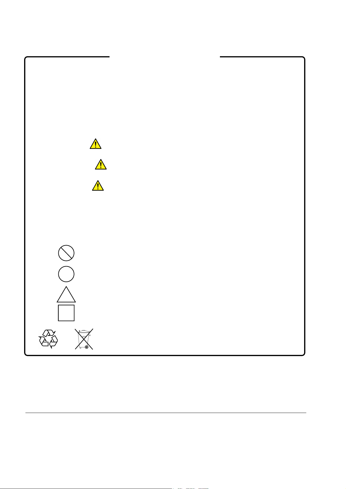
Safety Symbols
To prevent the risk of personal injury or loss related to equipment malfunction, Anritsu Corporation uses the following
safety symbols to indicate safety-related information. Ensure that you clearly understand the meanings of the
symbols BEFORE using the equipment. Some or all of the following symbols may be used on all Anritsu
equipment. In addition, there may be other labels attached to products that are not shown in the diagrams in this
manual.
Symbols used in manual
DANGER
WARNING
CAUTION
This indicates a very dangerous procedure that could result in serious injury or
death if not performed properly.
This indicates a hazardous procedure that could result in serious injury or death if
not performed properly.
This indicates a hazardous procedure or danger that could result in light-to-severe
injury, or loss related to equipment malfunction, if proper precautions are not taken.
Safety Symbols Used on Equipment and in Manual
The following safety symbols are used inside or on the equipment near operation locations to provide information
about safety items and operation precautions. Ensure that you clearly understand the meanings of the symbols
and take the necessary precautions BEFORE using the equipment.
This indicates a prohibited operation. The prohibited operation is indicated
symbolically in or near the barred circle.
This indicates an obligatory safety precaution. The obligatory operation is
indicated symbolically in or near the circle.
This indicates a warning or caution. The contents are indicated symbolically in or
near the triangle.
This indicates a note. The contents are described in the box.
These indicate that the marked part should be recycled.
MG3641A/MG3642A
Synthesized Signal Generator
Operation Manual
10 March 1997 (First Edition)
7 December 2007 (13th Edition)
Copyright © 1997-2007, ANRITSU CORPORATION.
All rights reserved. No part of this manual may be reproduced without the prior written permission of the
publisher.
The contents of this manual may be changed without prior notice.
Printed in Japan
ii
For Safety
WARNING
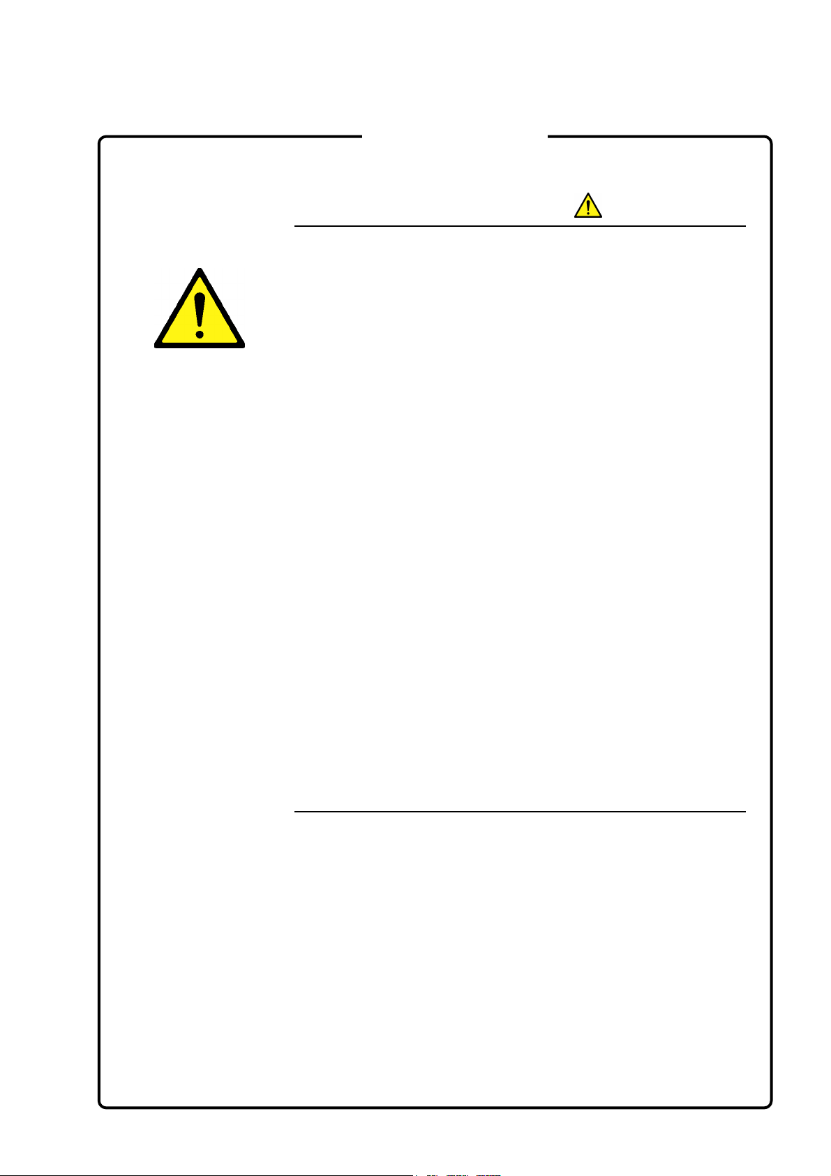
1. ALWAYS refer to the operation manual when working near locations
at which the alert mark shown on the left is attached. If the advice in
the operation manual is not followed there is a risk of personal injury
or reduced equipment performance. The alert mark shown on the
left may also be used with other marks and descriptions to indicate
other dangers.
2. IEC 61010 Standard
The IEC 61010 standard specifies four categories to ensure that an
instrument is used only at locations where it is safe to make
measurements. This instrument is designed for measurement
category I (CAT I). DO NOT use this instrument at locations
specified as category II, III, or IV as defined below.
Measurement category I (CAT I):
Secondary circuits of a device that is not directly connected to a
power outlet.
Measurement category II (CAT II):
Primary circuits of a device that is directly connected to a power outlet,
e.g., portable tools or home appliance.
Measurement category III (CAT III):
Primary circuits of a device (fixed equipment) to which power is
supplied directly from the distribution panel, and circuits running from
the distribution panel to power outlet.
Measurement category IV (CAT IV):
Building service-line entrance circuits, and circuits running from the
service-line entrance to the meter or primary circuit breaker
(distribution panel).
iii
For Safety
WARNING
Electric Shock
Repair
Calibration
3. To ensure that the instrument is earthed, always use the supplied 3-
pin power cord, and insert the plug into an outlet with an earth
terminal. If power is supplied without earthing the equipment, there
is a risk of receiving a severe or fatal electric shock or causing
damage to the internal components.
4. This equipment cannot be repaired by the operator. DO NOT attempt
to remove the equipment covers or unit covers or to disassemble
internal components. Only qualified service personnel with a
knowledge of electrical fire and shock hazards should service this
equipment. There are high-voltage parts in this equipment presenting
a risk of severe injury or fatal electric shock to untrained personnel. In
addition, there is a risk of damage to precision components.
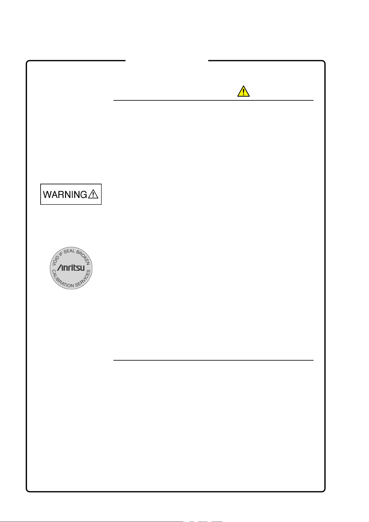
5. The performance-guarantee seal verifies the integrity of the equipment.
To ensure the continued integrity of the equipment, only Anritsu service
personnel, or service personnel of an Anritsu sales representative,
should break this seal to repair or calibrate the equipment. If the
performance-guarantee seal is broken by you or a third party, the
performance of the equipment cannot be guaranteed.
Falling Over
6. This equipment should always be positioned in the correct manner.
If the cabinet is turned on its side, etc., it will be unstable and may be
damaged if it falls over as a result of receiving a slight mechanical
shock.
Always set up the equipment in a position where the power switch
can be reached without difficulty.
iv
Fuse Replacement
Cleaning
For Safety
CAUTION
1. Always remove the mains power cable from the power outlet before
replacing blown fuses. There is a risk of electric shock if fuses are
replaced with the power cable connected. Always use new fuses of
the type and rating specified on the rear panel of the instrument.
There is a risk of fire if a fuse of a different rating is used.
T5A indicates a time-lag fuse.
2. Keep the power supply and cooling fan free of dust.
Clean the power inlet regularly. If dust accumulates around the
•
power pins, there is a risk of fire.
Keep the cooling fan clean so that the ventilation holes are not
•
obstructed. If the ventilation is obstructed, the cabinet may
overheat and catch fire.
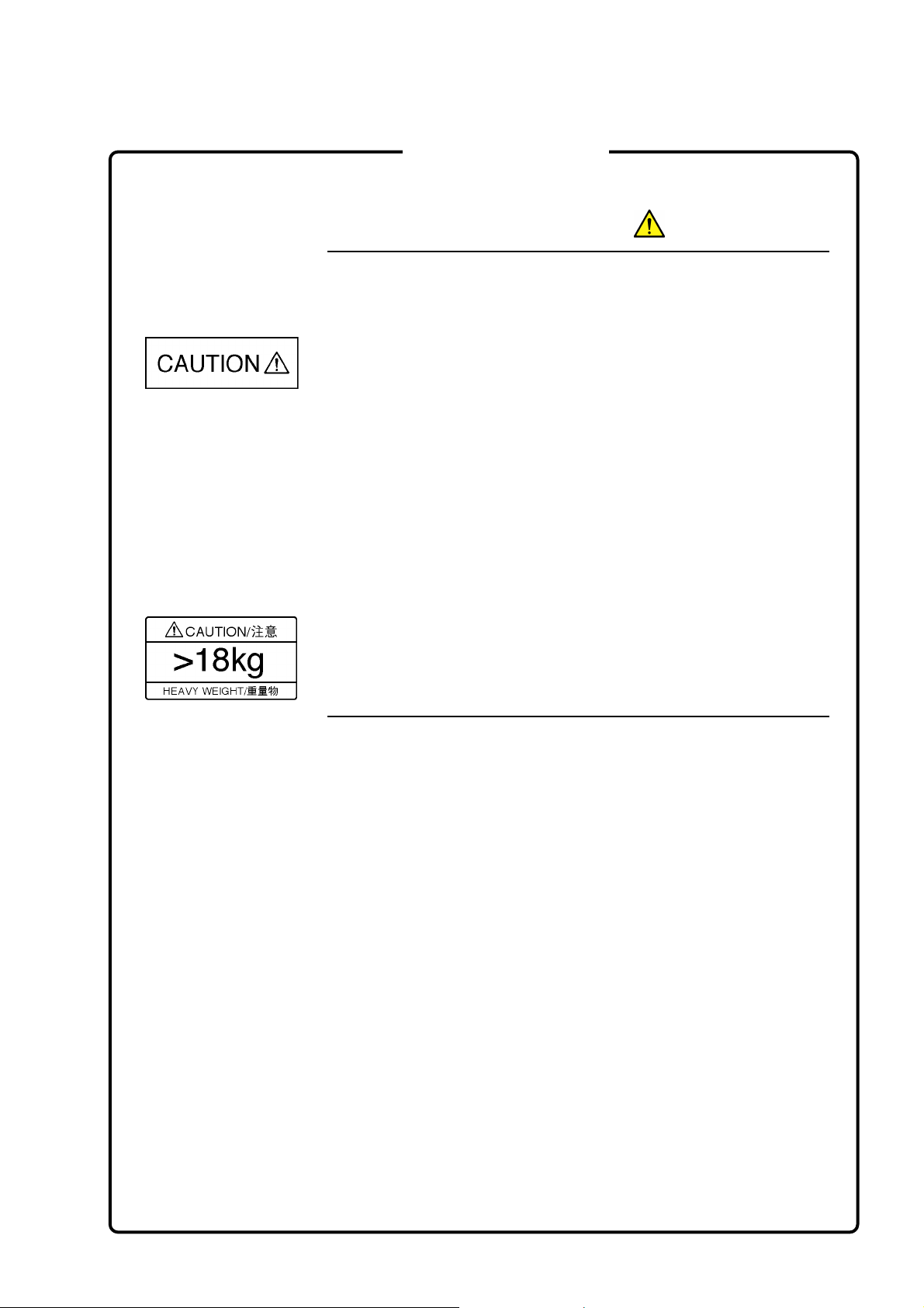
3. Use two or more people to lift and move this equipment, or use a
trolley. There is a risk of back injury, if this equipment is lifted by one
person.
v

For Safety
CAUTION
Replacing Memory
Back-up Battery
Use in a residential
environment
This equipment uses a Poly-carbomonofluoride lithium battery to backup
the memory. This battery must be replaced by service personnel when
it has reached the end of its useful life; contact the Anritsu sales section
or your nearest representative.
Note: The battery used in this equipment has a maximum useful life of
7 years. It should be replaced before this period has elapsed.
This instrument is designed for an industrial environment.
In a residential environment this instrument may cause radio interference
in which case the user may be required to take adequate measures.
vi

Equipment Certificate
Anritsu Corporation certifies that this equipment was tested before
shipment using calibrated measuring instruments with direct traceability
to public testing organizations recognized by national research
laboratories, including the National Institute of Advanced Industrial
Science and Technology, and the National Institute of Information and
Communications Technology, and was found to meet the published
specifications.
Anritsu Warranty
Anritsu Corporation will repair this equipment free-of-charge if a
malfunction occurs within one year after shipment due to a manufacturing
fault, under the condition that this warranty is void when:
The fault is outside the scope of the warranty conditions described in
•
the operation manual.
The fault is due to mishandling, misuse, or unauthorized modification
•
or repair of the equipment by the customer.
The fault is due to severe usage clearly exceeding normal usage.
•
The fault is due to improper or insufficient maintenance by the
•
customer.
The fault is due to natural disaster including fire, flooding, earthquake,
•
etc.
The fault is due to use of non-specified peripheral equipment,
•
peripheral parts, consumables, etc.
The fault is due to use of a non-specified power supply or in a non-
•
specified installation location.
In addition, this warranty is valid only for the original equipment
purchaser. It is not transferable if the equipment is resold.
Anritsu Corporation shall assume no liability for injury or financial loss of
the customer due to the use of or a failure to be able to use this equipment.
Anritsu Corporation Contact
In the event that this equipment malfunctions, contact an Anritsu Service
and Sales office. Contact information can be found on the last page of
the printed version of this manual, and is available in a separate file on
the CD version.
vii

Notes On Export Management
r
This product and its manuals may require an Export License/Approval by
the Government of the product's country of origin for re-export from you
country.
Before re-exporting the product or manuals, please contact us to confirm
whether they are export-controlled items or not.
When you dispose of export-controlled items, the products/manuals need
to be broken/shredded so as not to be unlawfully used for military purpose.
viii
Crossed-out Wheeled Bin Symbol
Equipment marked with the Crossed-out Wheeled Bin Symbol complies
with council directive 2002/96/EC (the “WEEE Directive”) in European
Union.
For Products placed on the EU market after August 13, 2005, please
contact your local Anritsu representative at the end of the product's
useful life to arrange disposal in accordance with your initial contract and
the local law.
ix
CE Conformity Marking
Anritsu affixes the CE conformity marking on the following product(s) in
accordance with the Council Directive 93/68/EEC to indicate that they
conform to the EMC and LVD directive of the European Union (EU).
CE marking
1. Product Model
Model: MG3641A/MG3642A Synthesezed Signal
Generator
2. Applied Directive
EMC: Directive 2004/108/EC
LVD: Directive 2006/95/EC
3. Applied Standards
EMC:Emission: EN 61326-1: 2006 (Class A)
•
Immunity:EN 61326-1: 2006 (Table 2)
IEC 61000-4-2 (ESD) B
IEC 61000-4-3 (EMF) A
IEC 61000-4-4 (Burst) B
IEC 61000-4-5 (Surge) B
IEC 61000-4-6 (CRF) A
IEC 61000-4-8 (RPFMF) A
IEC 61000-4-11 (V dip/short) B, C
*: Performance Criteria
A: During testing, normal performance within the
specification limits.
B: During testing, temporary degradation, or loss of
function or performance which is self-recovering.
C: During testing, temporary degradation, or loss of
function or performance which requires operator
intervention or system reset occurs.
Performance Criteria*
x

Harmonic current emissions:
EN 61000-3-2: 2006 (Class A equipment)
LVD: EN 61010-1: 2001 (Pollution Degree 2)
•
4. Authorized representative
Name: Loic Metais
European Quality Manager
ANRITSU S.A. France
Address, city: 16/18 Avenue du Québec SILIC 720 Zone de
Courtaboeuf
91951 Les Ulis Cedex
Country: France
xi

C-tick Conformity Marking
Anritsu affixes the C-tick mark on the following product(s) in accordance
with the regulation to indicate that they conform to the EMC framework
of Australia/New Zealand.
C-tick marking
1. Product Model
Model: MG3641A/MG3642A Synthesezed Signal
Generator
2. Applied Standards
EMC:Emission: EN 61326-1: 2006 (Class A equipment)
xii

Power Line Fuse Protection
For safety, Anritsu products have either one or two fuses in the AC power
lines as requested by the customer when ordering.
Single fuse:
Double fuse:
Example 1: An example of the single fuse is shown below:
Example 2: An example of the double fuse is shown below:
A fuse is inserted in one of the AC power lines.
A fuse is inserted in each of the AC power lines.
Fuse Holder
Fuse Holders
xiii

xiv

TABLE OF CONTENTS
For Safety ................................................................................................................. iii
SECTION 1 GENERAL ............................................................................................. 1-1
1.1 Brief Description .............................................................................................................. 1-1
1.2 Operation Manual ............................................................................................................. 1-2
1.3 Composition of Devices ................................................................................................... 1-3
1.3.1 Standard Composition ...................................................................................... 1-3
1.3.2 Options ............................................................................................................. 1-4
1.4 Application Parts .............................................................................................................. 1-5
1.5 Specifications ................................................................................................................... 1-6
SECTION 2 PRECAUTION ....................................................................................... 2-1
2.1 Installation Precautions .................................................................................................... 2-1
2.1.1 Installation site environmental conditions ....................................................... 2-1
2.2 Safety Measures ................................................................................................................ 2-2
2.2.1 General power supply safety measures ............................................................ 2-2
2.2.2 Reverse power input to RF output connector ................................................... 2-2
2.3 Mounting the MG3641A/MG3642A in the Frame .......................................................... 2-3
2.4 Preparation Before Power-On .......................................................................................... 2-4
2.4.1 Connecting the Power Cord ............................................................................. 2-5
2.4.2 Fuse Replacement ............................................................................................ 2-6
SECTION 3 PANEL LAYOUT ................................................................................... 3-1
3.1 Panel Layout ..................................................................................................................... 3-1
3.1.1 Front panel layout ............................................................................................ 3-1
3.1.2 Rear panel layout ............................................................................................. 3-3
3.1.3 Panel layout diagram ........................................................................................ 3-4
SECTION 4 OPERATING INSTRUCTIONS ............................................................. 4-1
4.1 Turning Power On/Off ..................................................................................................... 4-1
4.1.1 Turning Power On ............................................................................................ 4-3
4.1.2 Turning Power Off ........................................................................................... 4-4
4.2 Explanation of Screens ..................................................................................................... 4-5
4.3 Initial Settings ................................................................................................................... 4-6
4.4 Setting the Frequency ....................................................................................................... 4-8
4.4.1 Setting the Frequency ....................................................................................... 4-8
4.4.2 Displaying the Frequency Relative Value ....................................................... 4-9
4.4.3 Frequency Offset ............................................................................................ 4-10
4.5 Setting the Output Level ................................................................................................. 4-11
4.5.1 Setting the Output Level ................................................................................ 4-11
4.5.2 Displaying the Output Level Relative Value ................................................. 4-12
4.5.3 Output Level Offset ....................................................................................... 4-13
I

4.5.4 Level Continuous Mode ................................................................................. 4-14
4.5.5 Switching the Output Signal On/Off .............................................................. 4-15
4.5.6 Special Functions Related to Level ................................................................ 4-16
4.6 Setting the Modulation ................................................................................................... 4-18
4.6.1 Outline of Modulation .................................................................................... 4-18
4.6.2 Setting the Modulation Function .................................................................... 4-19
4.6.3 Setting the Modulation Factor and Frequency Deviation .............................. 4-20
4.6.4 Setting Range of FM Frequency Deviation ................................................... 4-21
4.6.5 Polarity of Modulation Signal ........................................................................ 4-21
4.6.6 Pulse Modulation ........................................................................................... 4-22
4.7 Setting the Modulation Signal Source ............................................................................ 4-24
4.7.1 Internal Modulation Signal (Int1) .................................................................. 4-24
4.7.2 Internal Modulation Signals (Int2, Int3) ........................................................ 4-25
4.7.3 External Modulation Signals (Ext1, Ext2) ..................................................... 4-26
4.8 Setting the AF Output ..................................................................................................... 4-28
4.9 Memory Functions .......................................................................................................... 4-30
4.9.1 Outline of Memory Functions ........................................................................ 4-30
4.9.2 Storing in the Memory ................................................................................... 4-30
4.9.3 Recalling Memory Contents .......................................................................... 4-31
4.9.4 Clearing the Memory ..................................................................................... 4-33
4.9.5 Selecting the Memory Recall Mode ............................................................... 4-34
4.10 Sweep Functions ............................................................................................................. 4-35
4.10.1 Outline of Sweep Functions ........................................................................... 4-35
4.10.2 Setting and Executing the Sweep ................................................................... 4-36
4.10.3 Sweep Auxiliary Outputs ............................................................................... 4-39
4.11 Trigger Functions ........................................................................................................... 4-41
4.11.1 Outline of trigger function ............................................................................. 4-41
4.11.2 Registering the trigger program ..................................................................... 4-42
4.11.3 Executing the trigger program ....................................................................... 4-43
4.11.4 Checking the contents of the trigger program ................................................ 4-44
4.12 Miscellaneous Functions ................................................................................................ 4-45
4.12.1 Setting Display On/Off .................................................................................. 4-45
4.12.2 Setting Bell • Alarm On/Off ........................................................................... 4-46
4.12.3 Setting address and only mode of GPIB ........................................................ 4-47
4.12.4 Panel Lock ...................................................................................................... 4-48
4.13 Removing Reverse Power Protection (RPP) Circuit Operation ..................................... 4-49
4.14 Error Messages ............................................................................................................... 4-50
SECTION 5 MEASUREMENT .................................................................................. 5-1
5.1 Measurement of Sensitivity .............................................................................................. 5-1
5.1.1 Measuring 20 dB NQ sensitivity ...................................................................... 5-2
5.1.2 Measuring 12 dB SINAD sensitivity ............................................................... 5-3
II

5.2 Measuring the 1-signal Selectivity ................................................................................... 5-4
5.2.1 Measuring selectivity characteristics of the FM receiver in 20 dB
NQ method ....................................................................................................... 5-4
5.2.2 Measuring spurious response ........................................................................... 5-7
5.3 Measuring the 2-signal Sensitivity ................................................................................... 5-9
5.3.1 Measuring the sensitivity blocking of the FM receiver ................................... 5-9
5.3.2 Measuring the cross-modulation characteristics ............................................ 5-12
SECTION 6 GPIB...................................................................................................... 6-1
6.1 Outline of GPIB ................................................................................................................ 6-1
6.1.1 Overview .......................................................................................................... 6-1
6.1.2 GPIB functions ................................................................................................. 6-1
6.1.3 Setup example .................................................................................................. 6-2
6.1.4 Standard ........................................................................................................... 6-3
6.2 Device Message List ......................................................................................................... 6-4
6.2.1 Outline .............................................................................................................. 6-4
6.2.2 General Information On SCPI .......................................................................... 6-4
6.2.3 Command Structure ......................................................................................... 6-4
6.2.4 Writing Commands .......................................................................................... 6-5
6.2.5 Compounding Commands ................................................................................ 6-6
6.2.6 Parameter ......................................................................................................... 6-7
6.2.7 Unit ................................................................................................................... 6-7
6.2.8 Command Tree ................................................................................................. 6-8
6.3 Connecting the GPIB Cable ........................................................................................... 6-14
6.4 Device Message Format ................................................................................................. 6-15
6.4.1 Program message format ................................................................................ 6-15
6.4.2 Response message format .............................................................................. 6-18
6.5 Status Message ............................................................................................................... 6-20
6.5.1 Status register configuration .......................................................................... 6-20
6.5.2 IEEE488.2-based status register .................................................................... 6-21
6.5.3 SCPI standard status register .......................................................................... 6-22
6.5.4 Reading, writing, clearing, and resetting the status register .......................... 6-23
6.5.5 SCPI error messages ...................................................................................... 6-25
6.6 Initializing Device .......................................................................................................... 6-27
6.6.1 Bus initialization ............................................................................................ 6-27
6.6.2 Message initialization .................................................................................... 6-27
6.6.3 Device initialization ....................................................................................... 6-27
6.6.4 Device state at power-on ................................................................................ 6-27
6.7 Detailed Description of Commands ............................................................................... 6-28
6.7.1 Frequency subsystem ..................................................................................... 6-28
6.7.2 Output level subsystem .................................................................................. 6-32
6.7.3 AM subsystem ................................................................................................ 6-38
6.7.4 FM subsystem ................................................................................................ 6-39
6.7.5 PM subsystem ................................................................................................ 6-41
III

6.7.6 Modulation source subsystem ........................................................................ 6-42
6.7.7 MEMORY subsystem .................................................................................... 6-45
6.7.8 Display subsystem .......................................................................................... 6-47
6.7.9 System subsystem .......................................................................................... 6-48
6.7.10 Status subsystem ............................................................................................ 6-49
6.8 IEEE488.2 Common Command ..................................................................................... 6-51
6.9 Sample Program ............................................................................................................. 6-53
6.10 GPIB Command Interchange Function .......................................................................... 6-56
6.10.1 Outline ............................................................................................................ 6-56
6.10.2 Restrictions in MG3633Acommand interchange mode ................................. 6-57
6.10.3 Restrictions in MG3631A/32A command interchange mode ........................ 6-60
SECTION 7 PERFORMANCE TEST ........................................................................ 7-1
7.1 Performance Test Required .............................................................................................. 7-1
7.2 Performance Test Device List .......................................................................................... 7-2
7.3 Performance Test .............................................................................................................. 7-3
7.3.1 Output frequency .............................................................................................. 7-4
7.3.2 Output level frequency characteristics ............................................................. 7-5
7.3.3 Output level accuracy ....................................................................................... 7-6
7.3.4 FM deviation and FM distortion ...................................................................... 7-8
7.3.5 AM modulation factor and AM distortion ..................................................... 7-10
SECTION 8 CALIBRATION ...................................................................................... 8-1
8.1 Calibration Required ........................................................................................................ 8-1
8.2 Calibration Device List ..................................................................................................... 8-1
8.3 Calibration ........................................................................................................................ 8-2
SECTION 9 STORAGE AND TRANSPORTATION .................................................. 9-1
9.1 Daily Servicing and Preventive Maintenance .................................................................. 9-1
9.2 Storage Precautions .......................................................................................................... 9-1
9.2.1 Precautions before storage ............................................................................... 9-1
9.2.2 Recommended storage conditions ................................................................... 9-2
9.3 Repacking and Transportation .......................................................................................... 9-2
9.3.1 Repacking ......................................................................................................... 9-2
9.3.2 Transportation .................................................................................................. 9-2
APPENDIX A INITIAL FACTORY SETTINGS ............................................................. A-1
APPENDIX B FUNCTION-KEY TRANSITION ............................................................ B-1
APPENDIX C FRONT AND REAR PANEL LAYOUT ..................................................C-1
APPENDIX D INDEX ................................................................................................... D-1
APPENDIX E PERFORMANCE TEST RESULT SHEET ............................................ E-1
IV
.

SECTION 1 GENERAL
SECTION 1
GENERAL
1.1 Brief Description
The MG3641A/MG3642A is a synthesized signal generator capable of outputing highly accurate, highly pure signals
over a broad frequency range.
The extremely excellent spurious characteristics and leakage characteristics offer to make the signal generator most
suitable to evaluate sensitivity characteristics and interference characteristics, which comprise the basic performance
of radio equipment.
Meanwhile, the signal generator can also be used to test communication systems operating with a variety of modulation
methods, such as a pager system, since it provides diverse modulation functions and frequency modulation with good
carrier frequency stability.
Its output level can be corrected over the entire frequency range. Because the signal generator allows to select high
level outputs and high resolutions, it can also serve to test various high frequency components.
The generator displays its basic functions, such as frequency, output level, and memory addresses, on a 7-segment
display unit. For those functions which require to have many parameters set, such as modulation, sweep function,
etc., it adopts the multimenu display. Moreover, the generator boasts of an outstanding operability, since it comes
equipped with a dedicated rotary knob and step keys for setting output levels.
1-1

SECTION 1 GENERAL
1.2 Operation Manual
This operation manual contains 9 sections and 5 appendixes. The format and outline of each section is described
below.
Table 1-1
Section Title Contents
1 GENERAL
2 PRECAUTION
3 PANEL LAYOUT
4 OPERATING
INSTRUCTIONS
5 MEASUREMENT
6 GPIB
7 PERFORMANCE TEST
8 CALIBRATION
9 STORAGE AND
TRANSPORTATION
APPENDIX A INITIALSETTINGS
B FUNCTION KEY
TRANSITION
DIAGRAM
C FRONT AND REAR
PANEL LAYOUT
D INDEX
E PERFORMANCE
TEST RESULT
SHEET
Description of the MG3641A/MG3642A (standard configuration,
specifications), optional accessories and peripheral equipment, and outline of
operation manual.
Operations to be performed before powering-up the MG3641A/MG3642A
Layout, function and method of preparative operation of components such as
keys, connectors, knobs, and indicators on both the front and rear panels.
Details of manual operation (local operation) of the front and rear panels. (Except
for remote control by GPIB)
Explains how to measure the sensitivity and selectivity, giving typical
examples using the signal generator
Remote-control operational procedure and description of device messages
Description of the measuring unit and performance test required to test the
performance of this device
Description of the calibration as the preventive maintenance to prevent the
performance from reducing.
Daily maintenance, long period storage, re-packing and transportation
1-2

1.3 Composition of Devices
The composition of standard accessories to the MG3641A/MG3642A will be explained in this section.
1.3.1 Standard Composition
The table below shows the standard composition of devices for the MG3641A/MG3642A.
Table 1-2. Standard Composition of Devices
Item Model/Symbol Product Name Q'ty Remarks
Main unit MG3641A/
MG3642A
Accessories Power cord 1 Length: approx. 2.6 m
B0325 GPIB shield cap 1
F0013 Fuse 1
or
F0012
W1137AE Operation manual 1 English version
W1137BE Service manual 1 English version
Synthesized signal generator 1
Two of 5 A (T5 A 250 V) for 100 VAC system
or
Two of 3.15 A (T3.15 A 250 V), for 200 VAC
system
SECTION 1 GENERAL
1-3

SECTION 1 GENERAL
1.3.2 Options
The table below lists options for the MG3641A/MG3642A.
Table 1-3. Options
Option
No.
01 MG3641A/ Reference Crystal Oscillator
Model number/
Order number
MG3642A-01
Name
Frequency: 10 MHz
Aging rate: 5×10
Temperature caracteristics: ±5×10⁻⁹ (at 0 to 50°C)
11 MG3641A/ Pulse ON/OFF ratio: >80 dB
MG3642A-11
modulator
Rise time/fall time: <100 ns
Minimum pulse width: <500 ns
Pulse repetition frequency: DC to 1 MHz
Maximum delay time: <100 ns
Overshoot/ringing: <20 %
Video feed through: <20 %
Pulse modulation signal: External, BNC connector on
21 MG3641A/
MG3642A-21
AF synthesizer
Frequency : 0.01 Hz to 400 kHz (sine wave)
: 0.01 Hz to 50 kHz
Resolution : 0.01 Hz
Wave form: sine wave, triangular wave, square wave,
sawtooth wave
Frequency accuracy: Equal to the accuracy of the refere-
22
MG3641A/
FSK encoder
2-level FSK, 4-level FSK
MG3642A-22
–10
/day
the rear panel, 50 Ω/600 Ω,
TTL(Positive logic)
(triangular, square, sawtooth wave)
nce oscillator.
1-4
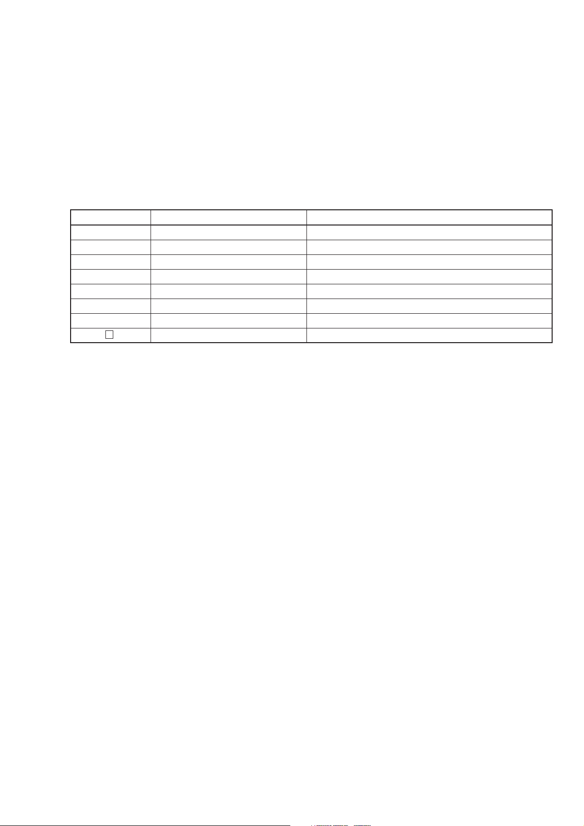
SECTION 1 GENERAL
1.4 Application Parts
The table below lists application parts for the MG3641A/MG3642A, which are all optional purchase items.
Table 1-4. Application Parts
Model/Symbol Product Name Remarks
J0576B Coaxial cord N-P•5D-2W•N-P, 1 m
J1027A Coaxial cord BNC-P•RG58A/U•BNC-P, 1 m
J0007 GPIB cable 408JE-101, 1 m
J0008 GPIB cable 408JE-102, 2 m
MP51A Pad Conversion from 75 Ω system to 50 Ω system
MP52A Pad Conversion from 50 Ω system to 75 Ω system
MA1612A Four-port junction pad 5 to 3000 MHz, 50 Ω
MP721 Fixed attenuator DC to 12.4 GHz, 3, 6, 10, 20, 30, 40, 50, 60 dB
1-5

SECTION 1 GENERAL
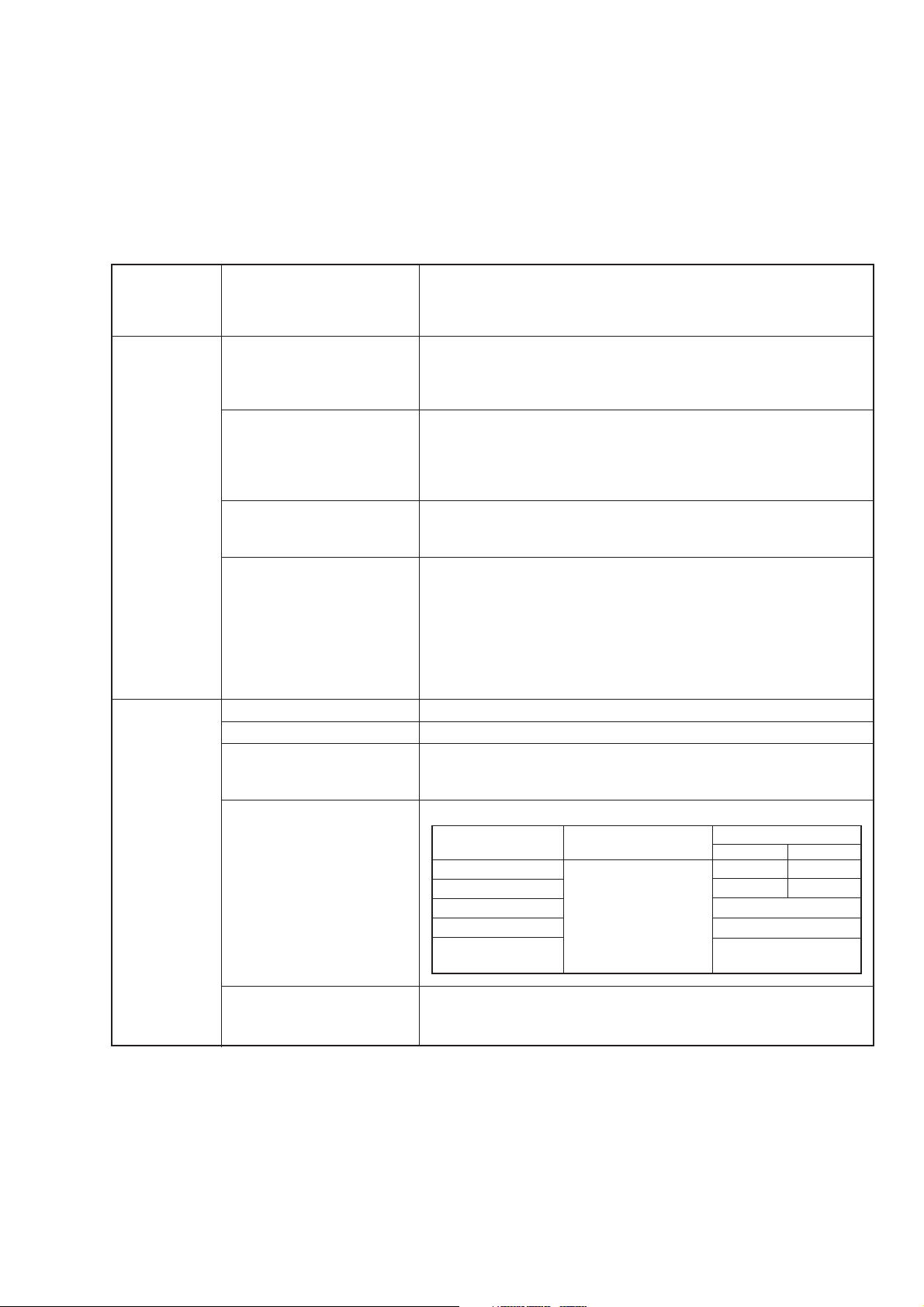
1.5 Specifications
Carrier Range 125 kHz to 1040 MHz: MG3641A
Frequency
Resolution 0.01 Hz
Accuracy Dependent on the accuracy of the reference oscillator.
Internal reference Frequency 10 MHz
oscillator
*1
External reference input 5/10 MHz, ±10 ppm, ≥0.7 Vp–p/50 Ω (AC coupling)
Buffer output 10 MHz, TTL level (DC coupling)
Switching time Response time from last command, till the preset frequency ±0.1 ppm
Output level Range –143 to +17 dBm (Permissible setting range: –143 to +23 dBm)
Unit dBm, dBµ, V, mV, µV
Resolution 0.01dB
Frequency response With reference to 0 dBm
Accuracy With pulse modulation off
Impedance 50 Ω, type N connector
Switching time Response time from last command, till the final level ±0.5 dB is
Special setting mode Level continuous mode:
*1 Available up to 5×10
*2 Only with Pulse Modulator(Opt. 11) installed
125 kHz to 2080 MHz: MG3642A
In the FM modulation,
Accuracy of reference frequency ±(0.3 % of FM deviation setting +5 Hz)
Aging rate ±5×10⁻⁹/day
Startup characteristics 1×10⁻⁷/10 min. (reference after 24-hour
operation)
Temperature stability ±3×10⁻⁸ (0 to 50°C)
BNC connector on the rear panel
BNC connector on the rear panel
is obtained, under external control:
<40 ms
(Switching between terminated-voltage display and open-voltage
display is possible for dBµ, V, mV and µV)
±0.5 dB
±1.0 dB (With pulse modulation on)
*2
±1 dB (≤+17 dBm, ≥–127 dBm)
±3 dB (<–127 dBm)
With pulse modulation on
*2
±1 dB (≤+12 dBm, ≥–127 dBm)
±3 dB (<–127 dBm)
VSWR: <1.5 (≤–3 dBm)
<2.5 (>–3 dBm)
obtained, under external control:
<50 ms (Normal mode)
<100 ms (Level safety mode)
<10 ms (continuous mode)
Level can be varied over a range of the set value ±10 dB, without
interruptions of the output
Level safety mode:
Level is narrowed to prevent spike-like signals from appearing when
the mechanical attenuator is working.
-10
/day with Reference Crystal Oscillator(Opt.01)
1-6
Specifications (continued)
SECTION 1 GENERAL
Output level
Interference radiation When measured with 50 Ω-terminated voltage using a two-loop
distortion
antenna of 25 mm in diameter at 25 mm away from the case:
<0.1 µV (At the output frequency)
<1 µV (Over the frequency range, at multimenu display OFF)
Signal Purity Spurious In CW mode and with reference to ≤+7 dBm:
Harmonics: <–30 dBc
Non-harmonics: <–100 dBc (≥15 kHz offset)
Those related to power: <–40 dBc (<15 kHz offset)
SSB phase noise In CW mode and with reference to 20 kHz offset:
<–140 dBc/Hz (≥10 MHz, <256 MHz)
<–136 dBc/Hz (≥256 MHz, <512 MHz)
<–130 dBc/Hz (≥512 MHz, ≤1040 MHz)
<–124 dBc/Hz (>1040 MHz, MG3642A)
Residual AM With reference to ≥500 kHz, CW mode, +7 dBm and in a 50 Hz to 15
kHz demodulation band:
<–80 dBc
Residual FM In CW mode and in a 300 Hz to 3 kHz demodulation band:
<4 Hzrms (≥10 MHz, <512 MHz)
<8 Hzrms (≥512 MHz, ≤1040 MHz)
<16 Hzrms (>1040 MHz, MG3642A)
In CW mode and in a 50 Hz to 15 kHz demodulation band:
<5 Hzrms (≥10 MHz, <512 MHz)
<10 Hzrms (≥512 MHz, ≤1040 MHz)
<20 Hzrms (>1040 MHz, MG3642A)
Amplitude Range 0 to 100 %
modulation
Resolution 0.1 %
Accuracy With reference to ≥0.4 MHz, ≤+7 dBm, AM≤90 %, Source=Int1 1
kHz, and in a 300 Hz to 3 kHz demodulation band:
±(5 % of set value +2 %)
Modulation frequency In ≤+7 dBm and ±1 dB Bandwidth:
response
Carrier frequency Lower limit frequency Upper limit frequency
≥
0.4 MHz, <0.5 MHz 2 kHz 1 kHz
≥
0.5 MHz, <2 MHz DC (Ext DC couple) 10 kHz 5 kHz
≥
2 MHz, <32 MHz 20 Hz (Ext AC couple) 20 kHz
≥
32 MHz, <64 MHz 50 kHz
≥
64 MHz 50 kHz
100 kHz (3 dB Bandwith)
AM = 30 % AM = 90 %
Distortion
With reference to ≥0.4 MHz, ≤+7 dBm, Source = Int1 1 kHz:
<–40 dB (AM = 30 %)
<–30 dB (AM = 90 %)
1-7

SECTION 1 GENERAL
Specifications (continued)
Amplitude Incidental FM With reference to ≥0.4 MHz, ≤+7 dBm, AM≤30 %, Source=Int1 1 kHz,
modulation
Modulation signal source Any one out of the internal modulation signal sources (Int1, Int2,
Modulation signal polarity Can be switched between positive and negative.
Frequency Range 0 to 125 Hz (≥125 kHz, <250 kHz)
modulation 0 to 250 Hz (≥250 kHz, <500 kHz)
Resolution 1 Hz (0 to 4.000 kHz deviation)
Accuracy With reference to ≥0.4 MHz, Source=Int1 1 kHz, and in a 300 Hz to
Modulation frequency In a ±1 dB bandwidth
response DC (Ext DC couple) or 20 Hz (Ext AC couple) to 20 kHz (≥0.4 MHz, <10 MHz)
Distortion With reference to ≥16 MHz:
Incidental AM With reference to ≥64 MHz, ≤+7 dBm, FM 100 kHz deviation,
External modulation group With reference to ≥10 MHz, Source=Ext DC coupling, and modulation
delay rate ≤100 kHz:
Modulation signal source Any one out of the internal modulation signal sources (Int1, Int2,
Modulation signal polarity Can be switched between positive and negative independently for
and in a 300 Hz to 3 kHz demodulation band:
<200 Hzpeak
Int3) and external modulation inputs (Ext1, Ext2) can be selected.
0 to 500 Hz (≥500 kHz, <1 MHz)
0 to 1 kHz (≥1 MHz, <2 MHz)
0 to 2 kHz (≥2 MHz, <4 MHz)
0 to 4 kHz (≥4 MHz, <8 MHz)
0 to 10 kHz (≥8 MHz, <16 MHz)
0 to 25.6 kHz (≥16 MHz, <32 MHz)
0 to 51.2 kHz (≥32 MHz, <64 MHz)
0 to 102 kHz (≥64 MHz, <128 MHz)
0 to 256 kHz (≥128 MHz, <256 MHz)
0 to 512 kHz (≥256 MHz, <512 MHz)
0 to 1024 kHz (≥512 MHz, ≤1040 MHz)
0 to 2048 kHz (>1040 MHz, MG3642A)
10 Hz (4.010 to 10.000 kHz deviation)
25 Hz (10.025 to 25.600 kHz deviation)
50 Hz (25.65 to 51.20 kHz deviation)
100 Hz (51.30 to 102.00 kHz deviation)
250 Hz (102.25 to 256.00 kHz deviation)
500 Hz (256.5 to 512.0 kHz deviation)
1 kHz (513 to 1024 kHz deviation)
1 kHz (1025 to 2048 kHz deviation, MG3642A)
3 kHz demodulation band:
±(5 % of set value +10 Hz) (≥0.4 MHz, <512 MHz)
±(5 % of set value +20 Hz) (≥512 MHz, ≤1040 MHz)
±(5 % of set value +40 Hz) (>1040 MHz, MG3642A)
DC (Ext DC couple) or 20 Hz (Ext AC couple) to 100 kHz (≥10 MHz)
–40 dB (FM=3.5 kHz deviation, and Source=Int1 1 kHz),
–45 dB (FM=22.5 kHz deviation, and Source=Int1 1 kHz)
Source=Int1 1 kHz, and in a 300 Hz to 3 kHz demodulation band:
<1 %peak
<30 µs
Int3) and external modulation inputs (Ext1, Ext2) can be selected for
each of FM1 and FM2.
FM1 and FM2.
1-8

SECTION 1 GENERAL
Specifications (continued)
Pulse See specifications of options.
modulation
Modulation Internal modulation (Int1) Frequency: 400 Hz/1 kHz (Switched over)
signal source
Internal modulation See specifications of options.
(Int2, Int3)
External modulation Optimum input level: Approx. 2 Vp–p
(Ext1, Ext2) Input impedance: 600 Ω, BNC connector on the front panel
AF Output Output signal source Any one out of the internal modulation signal sources (Int1, Int2,
Output level 0 to 4 Vp–p
Output level resolution 1 mVp–p
Output level accuracy In Source=Int1 1 kHz:
Impedance 600 Ω, BNC connector on the front panel
Simultaneous Simultaneous modulation, AM depth and FM deviation can be set
modulation independently for all combinations, except for a combination of AM
Sweep function Sweep parameter Frequency, Output level, and Memory
Sweep pattern Frequency sweep (Start/Stop): Liner (Stepsize specified, number
Sweep mode Auto, Single, Manual
Sweep time Setting range 1 ms to 600 s/point, Resolution 10 µs/point
Auxiliary outputs X-Output : BNC connector on the rear panel
Frequency accuracy: Equal to the accuracy of the reference oscillator.
Coupling: Switchable between AC/DC
Int3) and external modulation inputs (Ext1, Ext2) can be selected.
±(5% of set value + 2 mVp-p)
and pulse modulation.
of points specified)
Log (1 % specified)
Frequency sweep (Center/Span): Liner (Stepsize specified, number
of points specified)
Level sweep (Start/Stop): dB (Stepsize specified, number of points
specified)
Sweep in continuous mode (max. 20 dB width)
Level sweep (Center/Span): dB (Stepsize specified, number of points
specified)
Sweep in continuous mode (max. 20 dB width)
Memory sweep (Start/Stop)
(Actual sweep time depends on the sweep parameter switching times,
frequency, and output level.)
Staircase sawtooth wave worm
Start point of sweep: 0 V
Stop point of sweep: +10 V
Z-Output : BNC connector on the rear panel
TTL level
When sweeping: H-level
Blanking-Output : BNC connector on the rear panel
TTL level
When switched: L-level
Marker-Output : BNC connector on the rear panel
TTL level
When marker matches: H-level
1-9

SECTION 1 GENERAL
Specifications (continued)
Other functions Relative value display Carrier frequency and output level
Offset display Carrier frequency and output level
Memory 1000 panel setting conditions can be stored and recalled.
Recall mode: All panel settings, Frequency only, Frequency and Level.
Trigger function An external trigger signal (input from the BNC connector on the rear
panel, TTL level) can be used to execute a pre-programmed operation
sequence (except for operation of the power switch, Preset key, Local
key, and rotary knob).
Max. number of sequence steps of trigger program: 20 steps
Backup When switched on, the generator restores the same setting conditions
that existed immediately before it was last powered off.
However, the following are not restored:
• Data which was in the middle of entry
• Remote status
• Data which was in the middle of GPIB transfer
• Operating status of RPP
GPIB Can control all functions, except for pre-programmed operations
controlled by the trigger function, and operation of the power switch,
Local key, rotary knob, and knob resolution set keys.
Interface: SH1, AH1, T5, L3, TE0, SR1, RL1, PP0, DC1, DT1, C0,
E2
Reverse power Maximum reverse input 50 W (≤1040 MHz), 25 W (1040 to 2080 MHz, MG3642A only)
protection power ±50 Vac
General Power Voltage: *Vac (Up to max. 250 V)
Frequency: 47.5 to 63 Hz, 380 to 420 Hz
Capacity: 200 VAmax
Environmental performance Working temperature range: 0 to 50°C
Storage temperature range: –30 to 71°C
Conducted disturbance: EN 61326-1: 2006 (Class A)
Radiated disturbance: EN 61326-1: 2006 (Class A)
Harmonic Current Emission: EN 61000-3-2: 2006 (Class A)
Electrostatic Discharge: EN 61326-1: 2006 (Table 2)
Electromagnetic Field Immunity: EN 61326-1: 2006 (Table 2)
Fast Transient / Burst: EN 61326-1: 2006 (Table 2)
Surge: EN 61326-1: 2006 (Table 2)
Conducted RF: EN 61326-1: 2006 (Table 2)
Power Frequency Magnetic Field: EN 61326-1: 2006 (Table 2)
Voltage Dips / Short Interruptions: EN 61326-1: 2006 (Table 2)
Dimensions and mass 177 H×320 W×451 Dmm, ≤20 kg
* Please specify a nominal voltage in the range from 100 and 240 V when ordering the product.
1-10
1-10

SECTION 1 GENERAL
<Option>
■Option 01 (Reference crystal oscillator)
●Frequency 10MHz
●Aging rate 5×10
●Temperaturecharacteristics ±5×10
-10
/day
-9
(0 to 50°C)
■ Option 11 (Pulse modulator)
●Frequency 0.125 to 2080MHz
●On/Off ratio >80dB
●Rise/Fall time <100ns
●Min. pulse width <500ns
●Pulse repetition frequency DC to 1MHz
●Max. delay time <100ns
●Overshoot/ringing <20%
●Video feed through <20%
●Pulse modulation signal External, rear-panel BNC connector, 50/600 Ω, TTL (positive logic)
■Option 21 (AF synthesizer)
●Frequency 0.01Hz to 400kHz (sine wave)
0.01Hz to 50kHz (triangular wave, square wave, sawtooth wave)
●Resolution 0.01Hz
●Waveform Sine, triangular, square, sawtooth
●Frequency accuracy Same as reference oscillator
■Option 22 (FSK encoder)
●Frequency shift amount: Shifts frequency depending on data state, as below.
(Data21, Data20)=(0, 0): -FM deviation set value
(Data21, Data20)=(0, 1): -FM deviation set value/3
(Data21, Data20)=(1, 0): +FM deviation set value
(Data21, Data20)=(1, 1): +FM deviation set value/3
●Setting frequency: Set frequency for data input in the following timing.
Free: Shift frequency at data input.
Rise Trig: Shift frequency at rising edge of external clock.
Fall Trig: Shift frequency at falling edge of external clock.
●Baseband filter: Following filters can be used to pass signal.
Filter type: 10th-order Besser filter
Cutoff frequency: 100Hz to 30kHz(-3dB)
Set resolution: Upper 2 digits
●FM deviation accuracy: Same as that of MG3641A/MG3642A, with restriction of no baseband filter (by-passed)
●External modulation signal input
Data20: Rear-panel BNC connector (Int Mod Cont 2)
TTL level, pull-down
Data21: Rear-panel BNC connector (Int Mod Cont 1)
TTL level, pull-down
●External clock signal input
Ext Clock: Rear-panel BNC connector (Int Mod Cont 3)
TTL level, pull-up
1-11

SECTION 1 GENERAL
(Blank)
1-12.
 Loading...