Anritsu HFE0702 Brady

22 High Frequency Electronics
High Frequency Design
MICROSTRIP CIRCUITS
The Design, Fabrication and
Measurement of Microstrip
Filter and Coupler Circuits
By Dana Brady
CAP Wireless, Inc.
T
oday’s microwave
designers rely on
many tools to help
create effective circuits
and systems. They use
their libraries of published references, along
with powerful EDA
design tools and electromagnetic (EM) analysis
tools, combined with the lessons of their own
experience. Their work is verified with the
construction and testing of a finished circuit.
This article describes two microstrip designs
that were developed using different methods,
fabricated quickly using a p.c. board milling
machine, then measured to determine the
accuracy of the design methods.
The example designs are a classic hairpin
filter with a bandwidth of 3.7 to 4.2 GHz, and
a 1 to 8 GHz directional coupler using the
Schiffman sawtooth, or zig-zag, technique to
reduce the size. The hairpin filter was
designed and simulated using Agilent ADS 1.3
[1], with planar EM analysis using Sonnet
Lite [2]. The coupler used a design-rule-based
transformation, starting from an existing
stepped-line coupler design. Both circuits
were fabricated on a Protomat C100HF from
LPKF Laser & Electronics [3], with measured
results obtained using an HP (Agilent) 8753E
network analyzer.
Design example #1:
A 3.7 to 4.2 GHz hairpin filter
This filter was designed for a flat response
over the 3.7 to 4.2 GHz band, with low insertion loss and return loss better than 16 dB
across the band. The filter’s application is
image rejection at the input of a synthesized
block downconverter. A classic hairpin design
was chosen, since experience has shown that
it would meet the performance and size
requirements for this design.
The filter was designed using ADS 1.3,
with the resulting layout shown in Figure 1.
This, of course, is the familiar hairpin configuration. The area occupied by the filter is
approximately 500 by 1200 mils (0.5 x 1.2 in.),
plus sufficient area beyond the hairpin loops
to maintain consistent dielectric properties.
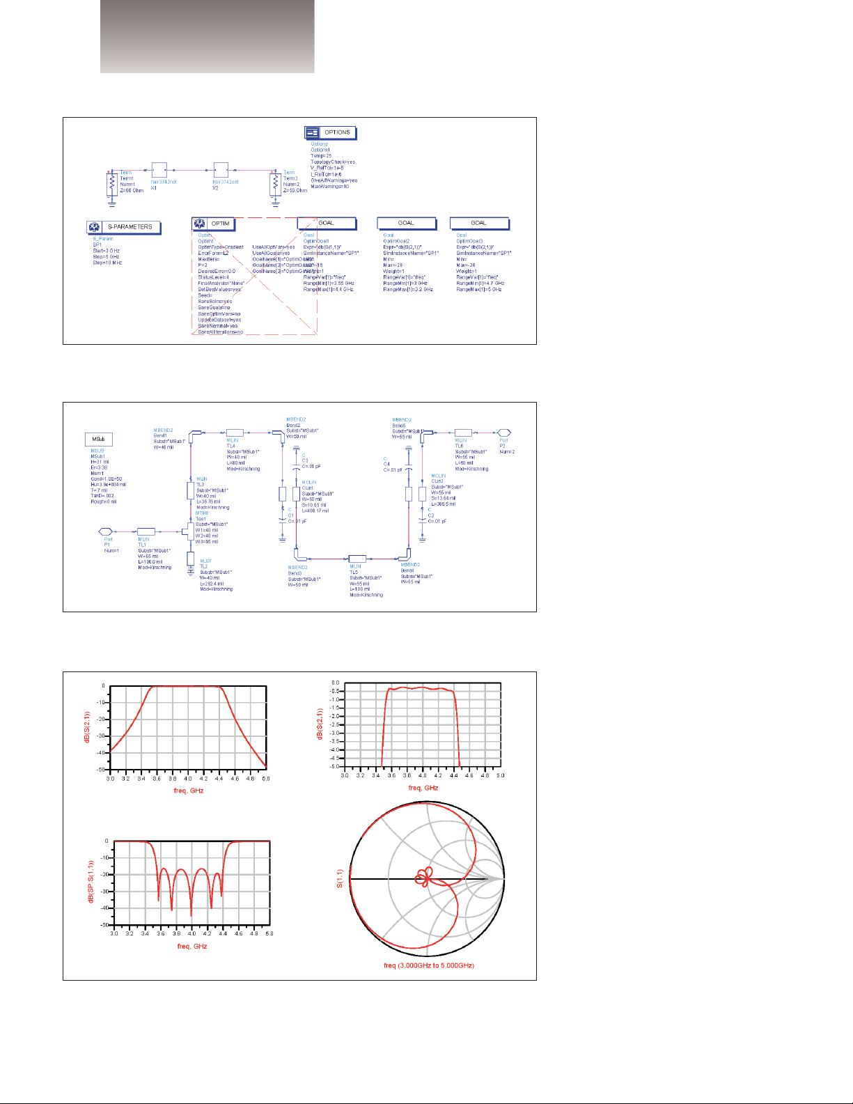
Figure 2 shows the design and optimization setup in ADS. Since this topology has
symmetry around the center, it was designed
as two sections, connected in a “back-to-back:
configuration. With this reduction in the size
of the mathematical problem, calculation time
is significantly reduced.
The optimization was set up to obtain a
minimum 16 dB return loss within a passband
of 3.55 to 4.4 GHz, and a minimum stopband
attenuation of 28 dB below 3.2 GHz and above
4.7 GHz. The optimization was set up for a frequency range of 3.0 to 5.0 GHz. A wider range
is not required to obtain the desired results.
These practical microstrip
examples provide a valu-
able tutorial on the use of
many different engineering
resources: published refer-
ences, comprehensive EDA
tools, EM analysis and rapid
prototyping equipment.
Figure 1 · Layout of the 3.7 to 4.2 GHz hairpin filter, designed with the help of ADS 1.3.
From July 2002 High Frequency Electronics.
Copyright © 2002 Summit Technical Media, LLC

24 High Frequency Electronics
High Frequency Design
MICROSTRIP CIRCUITS
The final ADS design for each
“half filter” is shown in Figure 3,
including the ports, microstrip lines,
tees, bends and stubs. Note the 0.1 pF
capacitances at the end of the stubs
to account for end effect (fringing
capacitance). These are also shown in
the layout diagram of Figure 1.
Modeled performance is shown in
Figure 4. These plots show the passband, stopband, return loss results of
the ADS simulation, along with a
Smith chart plot of input/output
impedance. These plots show that the
ADS model meets the filter’s design
criteria.
EM analysis
A detailed diagram of the filter
dimensions is shown in Figure 5. This
layout data was used to set up an
analysis of the circuit using the free
Sonnet Lite planar electromagnetic
field solver software from Sonnet
Software, Inc.
Figure 6 shows the results of EM
analysis. The passband response is
slightly narrower than predicted by
ADS, but will cover the desired 3.7 to
4.2 GHz band if the performance of
the fabricated circuit matches this
analysis. Passband flatness is very
close to that modeled by ADS. Return
loss response is less symmetrical
across the passband than the ADS
simulation, but it remains at 16 dB or
better.
Fabricating a test filter
To compare the performance of
the modeled hairpin filter design
with its real-world counterpart, a test
filter was fabricated on a typical
microwave laminate, using a p.c.
board milling machine (LPKF
Protomat C100HF—see the sidebar
on page 29).
Layout data from ADS (Figure 1)
was used to create the necessary
driver files for the milling machine.
These dimensions were transferred
directly from ADS into the LPKF
setup software. Figure 7 is the layout
for fabrication of the board.
Figure 2 · Optimization setup in ADS. As noted in the text, the filter was simulated as two “mirror image” sections to exploit the filter’ symmetry.
Figure 3 · The ADS simulation definition of the final design. Simulated performance data and filter layout are derived from this data.
Figure 4 · Simulation results for the filter: (a) overall response, (b) passband
response and insertion loss, (c) return loss, and (d) Smith chart impedance
 Loading...