

Quad 8-Bit Multiplying CMOS
a
FEATURES
Four DACs in a 28 Pin, 0.6 Inch Wide DIP or 28-Pin JEDEC
Plastic Chip Carrier
61/4 LSB Endpoint Linearity
Guaranteed Monotonic
DACs Matched to Within 1%
Microprocessor Compatible
Read/Write Capability (with Memory)
TTL/CMOS Compatible
Four-Quadrant Multiplication
Single-Supply Operation (+5 V)
Low Power Consumption
Latch-Up Resistant
Available In Die Form
APPLICATIONS
Voltage Set Points in Automatic Test Equipment
Systems Requiring Data Access for Self-Diagnostics
Industrial Automation
Multichannel Microprocessor-Controlled Systems
Digitally Controlled Op Amp Offset Adjustment
Process Control
Digital Attenuators
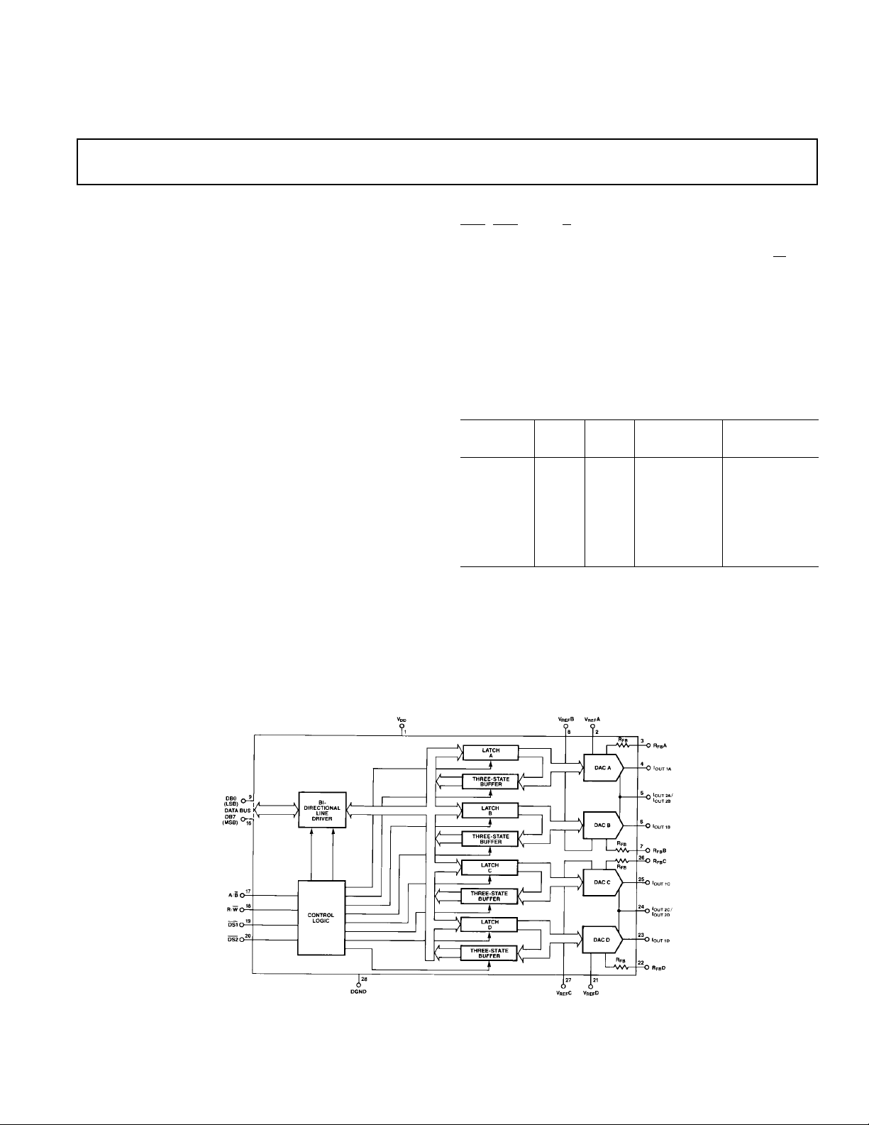
GENERAL DESCRIPTION
The DAC8408 is a monolithic quad 8-bit multiplying digital-toanalog CMOS converter. Each DAC has its own reference input,
feedback resistor, and onboard data latches that feature
read/write capability. The readback function serves as memory
for those systems requiring self-diagnostics.
D/A Converter with Memory
DAC8408
A common 8-bit TTL/CMOS compatible input port is used to
load data into any of the four DAC data-latches. Control lines
DS1, DS2, and A/B determine which DAC will accept data.
Data loading is similar to that of a RAMs write cycle. Data can
be read back onto the same data bus with control line R/
DAC8408 is bus compatible with most 8-bit microprocessors,
including the 6800, 8080, 8085, and Z80. The DAC8408 operates on a single +5 volt supply and dissipates less than 20 mW.
The DAC8408 is manufactured using PMI’s highly stable,
thin-film resistors on an advanced oxide-isolated, silicon-gate,
CMOS process. PMI’s improved latch-up resistant design eliminates the need for external protective Schottky diodes.
ORDERING INFORMATION
Temperature Package
Model INL DNL Range Description
DAC8408GP ±1/4 LSB ±1/2 LSB 0°C to +70°C 28-Pin Plastic DIP
DAC8408ET ±1/4 LSB ±1/2 LSB –40°C to +85°C 28-Pin Cerdip
DAC8408AT2±1/4 LSB ±1/2 LSB –55°C to +125°C 28-Pin Cerdip
DAC8408FT ±1/2 LSB ±1 LSB –40°C to +85°C 28-Pin Cerdip
DAC8408BT2±1/2 LSB ±1 LSB –55°C to +125°C 28-Pin Cerdip
DAC8408FPC3±1/2 LSB ±1 LSB –40°C to +85°C 28-Contact PLCC
DAC8408FS ±1/2 LSB ±1 LSB –40°C to +85°C 28-Pin SOL
DAC8408FP ±1/2 LSB ± 1 LSB –40°C to +85°C 28-Pin Plastic DIP
NOTES
1
Burn-in is available on commercial and industrial temperature range parts
in cerdip, plastic DIP, and TO-can packages. For outline information see Package Information section.
2
For devices processed in total compliance to MIL-STD-883, add /883 after
part number. Consult factory for 883 data sheet.
3
For availability and burn-in information on SO and PLCC packages, contact
your local sales office.
1
W. The
FUNCTIONAL BLOCK DIAGRAM
DAC8408
REV. A
Information furnished by Analog Devices is believed to be accurate and
reliable. However, no responsibility is assumed by Analog Devices for its
use, nor for any infringements of patents or other rights of third parties
which may result from its use. No license is granted by implication or
otherwise under any patent or patent rights of Analog Devices.
One Technology Way, P.O. Box 9106, Norwood, MA 02062-9106, U.S.A.
Tel: 617/329-4700 Fax: 617/326-8703

DAC8408
ELECTRICAL CHARACTERISTICS
(@ VDD = +5 V; V
= 610 V; V
REF
A, B, C, D = 0 V; TA = –558C to +1258C apply for
OUT
DAC8408AT/BT, TA = –408C to +858C apply for DAC8408ET/FT/FP/FPC/FS; TA = 08C to +708C apply for DAC8408GP, unless otherwise noted.
Specifications apply for DAC A, B, C, & D.)
DAC8408
Parameter Symbol Conditions Min Typ Max Units
STATIC ACCURACY
Resolution N 8 Bits
Nonlinearity
1, 2
INL DAC8408A/E/G ±1/4 LSB
DAC8408B/F/H ±1/2 LSB
Differential DNL DAC8408A/E/G ±1/2 LSB
Nonlinearity DAC8408B/F/H ±1 LSB
Gain Error G
Gain Tempco
3, 6
TC
FSE
GFS
(Using Internal RFB) ±1 LSB
±2 ±40 ppm/°C
Power Supply Rejection
(∆V
= ±10%) PSR 0.001 %FSR/%
DD
I
OUT 1A, B, C, D
Leakage Current
13
I
LKG
TA =+25°C ±30 nA
TA = Full Temperature Range ±100 nA
REFERENCE INPUT
Input Voltage Range ±20 V
Input Resistance Match
Input Resistance R
4
IN
R
A, B, C, D
±1%
6 1014kΩ
DIGITAL INPUTS
Digital Input Low V
Digital Input High V
Input Current
Input Capacitance
5
6
IL
IH
2.4 V
TA = +25°C ±0.01 ±1.0 µA
I
IN
C
IN
TA = Full Temperature Range ±10.0 µA
0.8 V
8pF
DATA BUS OUTPUTS
Digital Output Low V
Digital Output High V
Output Leakage Current I
OL
OH
LKG
16 mA Sink 0.4 V
400 µA Source 4 V
TA = +25°C ±0.005 ± 1.0 µA
TA = Full Temperature Range ±0.075 ± 10.0 µA
DAC OUTPUTS
Propagation Delay
Settling Time
Output Capacitance C
6
11,12
7
t
t
PD
S
OUT
150 180 ns
190 250 ns
DAC Latches All “0s” 30 pF
DAC Latches All “1s” 50 pF
AC Feedthrough FT (20 V
SWITCHING CHARACTERISTICS
Write to Data Strobe Time t
Data Valid to Strobe Set-Up Time t
Data Valid to Strobe Hold Time t
DAC Select to Strobe Set-Up Time t
DAC Select to Strobe Hold Time t
Write Select to Strobe Set-Up Time t
Write Select to Strobe Hold Time t
Read to Data Strobe Width t
Data Strobe to Output Valid Time t
Output Data to Deselect Time t
Read Select to Strobe Set-Up Time t
Read Select to Strobe Hold Time t
Specifications subject to change without notice.
6, 10
or TA = +25°C90 ns
DS1
t
DS2
DSU
DH
AS
AH
WSU
WH
RDS
CO
OTD
RSU
RH
TA = Full Temperature Range 145 ns
TA = +25°C 150 ns
T
TA = +25°C 220 ns
T
TA = +25°C 320 ns
T
TA = +25°C 200 ns
T
@ F = 100 kHz) 54 dB
p-p
= Full Temperature Range 175 ns
A
10 ns
0ns
0ns
0ns
0ns
= Full Temperature Range 350 ns
A
= Full Temperature Range 430 ns
A
= Full Temperature Range 270 ns
A
0ns
0ns
–2–
REV. A
DAC8408
ELECTRICAL CHARACTERISTICS
@ VDD = +5 V; V
= 610 V; V
REF
A, B, C, D = 0 V; TA = –558C to +1258C apply for
OUT
DAC8408AT/BT, TA = –408C to +858C apply for DAC8408ET/FT/FP/FPC/FS; TA = 08C to +708C apply for DAC8408GP, unless otherwise noted.
Specifications apply for DAC A, B, C, & D.
Continued
DAC8408
Parameter Symbol Conditions Min Typ Max Units
POWER SUPPLY
Voltage Range V
Supply Current
Supply Current
8
9
DD
I
DD
I
DD
TA = +25°C 1.0 mA
4.5 5.5 V
50 µA
TA = Full Temperature Range 1.5 mA
NOTES
1
This is an end-point linearity specification.
2
Guaranteed to be monotonic over the full operating temperature range.
3
ppm/°C of FSR (FSR = Full Scale Range = V
4
Input Resistance Temperature Coefficient = +300ppm/ °C.
5
Logic Inputs are MOS gates. Typical input current at +25 °C Is less than 10 nA.
6
Guaranteed by design.
-1 LSB.)
REF
7
From Digital Input to 90% of final analog output current.
8
All Digital Inputs “0” or VDD.
9
All Digital Inputs VIH or VIL.
10
See Timing Diagram.
11
Digital Inputs = 0 V to VDD or VDD to 0 V.
12
Extrapolated: tS (1/2 LSB) = tPD + 6.2τ where τ = the measured first time con-
stant of the final RC decay.
13
All Digital Inputs = 0 V; V
Specifications subject to change without notice.
= +10 V.
REF
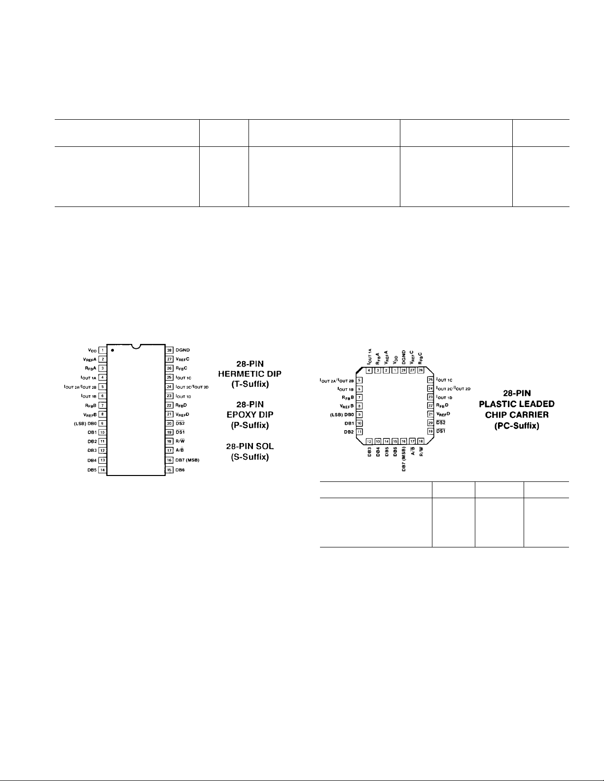
PIN CONNECTIONS
DAC8408
TOP VIEW
(Not to Scale)
ABSOLUTE MAXIMUM RATINGS
(TA = +25°C, unless otherwise noted.)
VDD to I
V
to DGND . . . . . . . . . . . . . . . . . . . . . . . . . . . . . .0 V, +7 V
DD
I
OUT 1A
I
OUT 1C
R
A, RFBB, RFBC, RFBD to I
FB
I
, I
OUT 2A
I
OUT 2C
DB0 through DB7 to DGND . . . . . . . . –0.3 V to V
OUT 2A
, I
OUT 1B
, I
OUT 2B
, I
, I
OUT 2B
, I
OUT 2C
, I
OUT 2D
. . . . . . . . . .0 V, +7 V
,
to DGND . . . . . . . . . –0.3 V to VDD +0.3 V
OUT 1D
. . . . . . . . . . . . . . . . . ±25 V
OUT
,
to DGND . . . . . . . . . –0.3 V to VDD + 0.3 V
OUT 2D
+ 0.3 V
DD
Control Logic
Input Voltage to DGND . . . . . . . . . . –0.3 V + V
V
REF
I
OUT 2A
A, V
REF
, I
B, V
OUT 2B
REF
, I
C, V
OUT 2C
REF
, I
D to
OUT 2D
. . . . . . . . . . . . . . . . ±25 V
+ 0.3 V
DD
Operating Temperature Range
Commercial Grade (GP) . . . . . . . . . . . . . . . . 0°C to +70°C
Industrial Grade (ET, FT, FP, FPC, FS) . –40°C to +85°C
Military Grade (AT, BT) . . . . . . . . . . . . . .–55°C to +125°C
Junction Temperature . . . . . . . . . . . . . . . . . . . . . . . . . +150°C
Storage Temperature . . . . . . . . . . . . . . . . . . .–65°C to +150°C
Lead Temperature (Soldering, 10 sec) . . . . . . . . . . . . . +300°C
Package Type uJA* u
JC
Units
28-Pin Hermetic DIP (T) 55 10 °C/W
28-Pin Plastic DIP (P) 53 27 °C/W
28-Pin SOL (S) 68 23 °C/W
28-Contact PLCC (PC) 66 29 °C/W
*θJA is specified for worst case mounting conditions, i.e., θJA is specified for
device in socket for cerdip and P-DIP packages; θJA is specified for device
soldered to printed circuit board for SOL and PLCC packages.
CAUTION
1. Do not apply voltages higher than V
–0.3 V potential on any terminal except V
+0.3 V or less than
DD
and RFB.
REF
2. The digital control inputs are diode-protected; however,
permanent damage may occur on unconnected inputs from
high energy electrostatic fields. Keep in conductive foam at
all times until ready to use.
3. Use proper antistatic handling procedures.
4. Absolute Maximum Ratings apply to both packaged devices
and DICE. Stresses above those listed under Absolute Maximum Ratings may cause permanent damage to the device.
REV. A
–3–
DAC8408
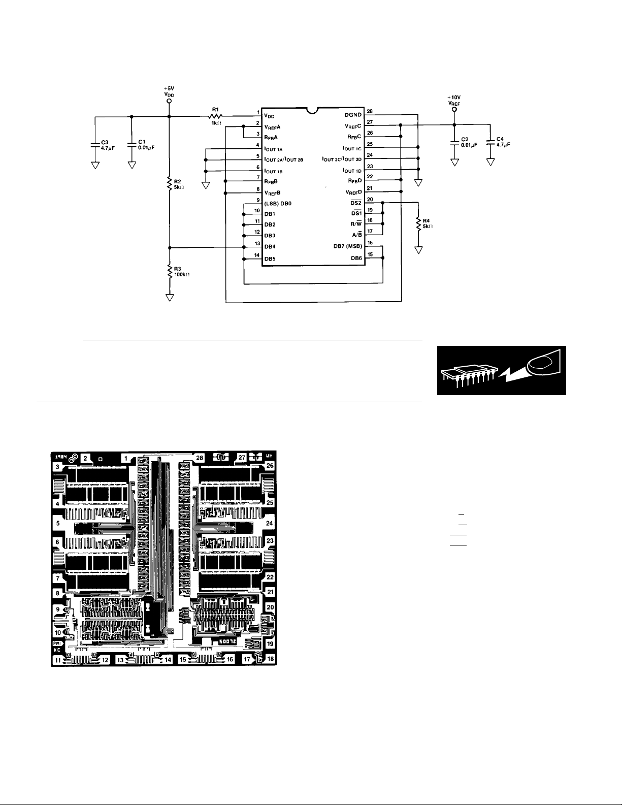
Burn-in Circuit
CAUTION
ESD (electrostatic discharge) sensitive device. Electrostatic charges as high as 4000 V readily
accumulate on the human body and test equipment and can discharge without detection.
Although the DAC8408 features proprietary ESD protection circuitry, permanent damage may
occur on devices subjected to high energy electrostatic discharges. Therefore, proper ESD
precautions are recommended to avoid performance degradation or loss of functionality.
WARNING!
ESD SENSITIVE DEVICE
DICE CHARACTERISTICS
DIE SIZE 0.130 × 0.124 inch, 16,120 sq. mils
(3.30
×
3.15 mm, 10.4 sq. mm)
1. V
2. V
DD
A 16. DB7 (MSB)
REF
15. DB6
3. RFBA 17. A/B
4. I
OUT 1A
5. I
OUT 2A/IOUT 2B
6. I
OUT 1B
B 21. V
7. R
FB
8. V
B 22. RFBD
REF
9. DB0 (LSB) 23. I
10. DB1 24. I
11. DB2 25. I
18. R/W
19. DS1
20. DS2
REF
OUT 1D
OUT 2C/IOUT 2D
OUT 1C
D
12. DB3 26. RFBC
13. DB4 27. V
REF
C
14. DB5 28. DGND
–4–
REV. A

DAC8408
WAFER TEST LIMITS
at VDD = +5 V; V
= 610 V; V
REF
A, B, C, D = 0 V; TA = +258C, unless otherwise noted. Specifications apply for
OUT
DAC A, B, C, & D.
DAC8408G
Parameter Symbol Conditions Limits Units
STATIC ACCURACY
Resolution N 8 Bits min
Nonlinearity
1
INL ±1/2 LSB max
Differential Nonlinearity DNL ±1 LSB max
Gain Error G
Power Supply Rejection PSR Using Internal R
(∆V
= ±10%)
DD
I
OUT 1A, B, C, D
2
Leakage Current I
V
FSE
LKG
REF
= +10 V
Using Internal R
FB
FB
±1 LSB max
0.001 %FSR/% max
All Digital Inputs = 0 V ±30 nA max
REFERENCE INPUT
Reference Input R
Resistance
3
Input Resistance Match R
IN
IN
6/14 kΩ min/max
±1 % max
DIGITAL INPUTS
Digital Input Low V
Digital Input High V
Input Current
4
IL
IH
I
IN
0.8 V max
2.4 V min
±1.0 µA max
DATA BUS OUTPUTS
Digital Output Low V
Digital Output High V
Output Leakage Current I
POWER SUPPLY
Supply Current
Supply Current
NOTES
1
This is an endpoint linearity specification.
2
FSR is Full Scale Range = V
3
Input Resistance Temperature Coefficient approximately equals +300 ppm/ °C.
4
Logic inputs are MOS gates.Typical input current at +25°C is less than 10 nA.
5
All Digital Inputs are either “0” or VDD.
6
All Digital Inputs are either VIH or VIL.
5
6
–1 LSB.
REF
I
I
OL
OH
LKG
DD
DD
1.6 mA Sink 0.4 V max
400 µA Source 4 V min
±1.0 µA max
50 µA max
1.0 mA max
Electrical tests are performed at wafer probe to the limits shown. Due to variations in assembly methods and normal yield loss, yield after packaging is not guaranteed
for standard product dice. Consult factory to negotiate specifications based on dice lot qualification through sample lot assembly and testing.
REV. A
–5–

DAC8408
TYPICAL PERFORMANCE CHARACTERISTICS
Supply Current vs. Logic Level
Analog Crosstalk vs. Frequency
–6–
REV. A

Timing Diagram
DAC8408
PARAMETER DEFINITIONS
RESOLUTION
Resolution is the number of states (2n) that the full-scale range
(FSR) of a DAC is divided (or resolved) into.
NONLINEARITY
Nonlinearity (Relative Accuracy) is a measure of the maximum
deviation from a straight line passing through the end-points of
the DAC transfer function. It is measured after adjusting for
ideal zero and full-scale and is expressed in LSB, %, or ppm of
full-scale range.
DIFFERENTIAL NONLINEARITY
Differential Nonlinearity is the worst case deviation of any adjacent analog outputs from the ideal 1 LSB step size. A specified
differential nonlinearity of ±1 LSB maximum over the operating
temperature range ensures monotonicity.
GAIN ERROR
Gain Error (full-scale error) is a measure of the output error between the ideal and actual DAC output. The ideal full-scale
output is V
OUTPUT CAPACITANCE
Output Capacitance is that capacitance between I
I
, or I
OUT 1C
–1 LSB.
REF
OUT 1D
and AGND.
OUT 1A
, I
OUT 1B
,
AC FEEDTHROUGH ERROR
This is the error caused by capacitance coupling from V
REF
to
the DAC output with all switches off.
SETTLING TIME
Settling Time is the time required for the output function of the
DAC to settle to within 1/2 LSB for a given digital input signal.
PROPAGATION DELAY
This is a measure of the internal delays of the DAC. It is defined
as the time from a digital input change to the analog output current reaching 90% of its final value.
CHANNEL-TO-CHANNEL ISOLATION
This is the portion of input signal that appears at the output of a
DAC from another DAC’s reference input. It is expressed as a
ratio in dB.
DIGITAL CROSSTALK
Digital Crosstalk is the glitch energy transferred to the output of
one DAC due to a change in digital input code from other
DACs. It is specified in nVs.
REV. A
–7–

DAC8408
CIRCUIT INFORMATION
The DAC8408 combines four identical 8-bit CMOS DACs
onto a single monolithic chip. Each DAC has its own reference
input, feedback resistor, and on-board data latches. It also features a read/write function that serves as an accessible memory
location for digital-input data words. The DAC’s three-state
readback drivers place the data word back onto the data bus.
D/A CONVERTER SECTION
Each DAC contains a highly stable, silicon-chromium, thin-film,
R-2R resistor ladder network and eight pairs of current steering
switches. These switches are in series with each ladder resistor
and are single-pole, double-throw NMOS transistors; the gates
of these transistors are controlled by CMOS inverters. Figure 1
shows a simplified circuit of the R-2R resistor ladder section,
and Figure 2 shows an approximate equivalent switch circuit.
The current through each resistor leg is switched between I
and I
gardless of the digital input logic states.
Each transistor switch has a finite “ON” resistance that can introduce errors to the DAC’s specified performance. These resistances must be accounted for by making the voltage drop across
each transistor equal to each other. This is done by binarilyscaling the transistor’s “ON” resistance from the most significant bit (MSB) to the least significant bit (LSB). With 10 volts
applied at the reference input, the current through the MSB
switch is 0.5 mA, the next bit is 0.25 mA, etc.; this maintains a
constant 10 mV drop across each switch and the converter’s accuracy is maintained. It also results in a constant resistance appearing at the DAC’s reference input terminal; this allows the
DAC to be driven by a voltage or current source, ac or dc of
positive or negative polarity.
Shown in Figure 3 is an equivalent output circuit for DAC A.
The circuit is shown with all digital inputs high. The leakage
current source is the combination of surface and junction leakages to the substrate. The 1/256 current source represents the
constant 1-bit current drain through the ladder terminating resistor. The situation is reversed with all digital inputs low, as
shown in Figure 4. The output capacitance is code dependent,
and therefore, is modulated between the low and high values.
. This maintains a constant current in each leg, re-
OUT 2
OUT 1
Figure 1. Simplified D/A Circuit of DAC8408
Figure 2. N-Channel Current Steering Switch
Figure 3. Equivalent DAC Circuit (AII Digital Inputs HIGH)
–8–
REV. A
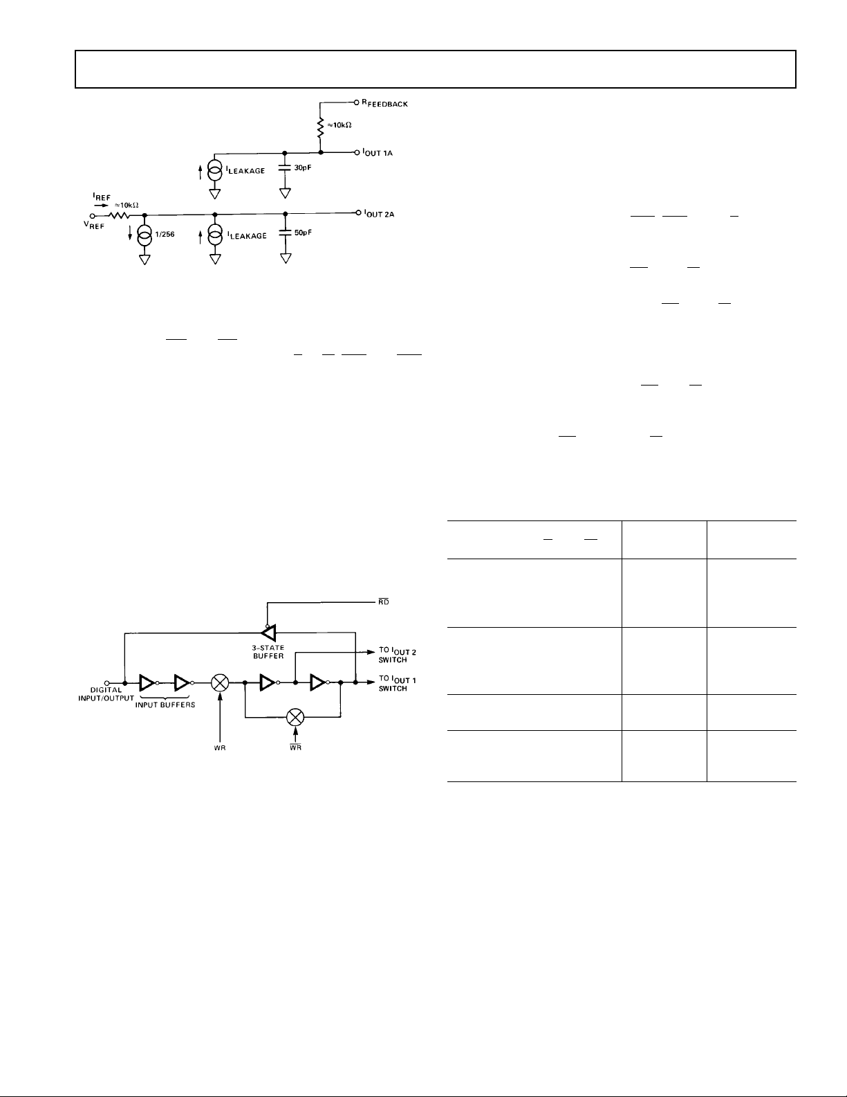
Figure 4. Equivalent DAC Circuit (AII Digital Inputs LOW)
DIGITAL SECTION
Figure 5 shows the digital input/output structure for one bit.
The digital WR,
internally generated from the external A/
signals. The combination of these signals decide which DAC is
selected. The digital inputs are CMOS inverters, designed such
that TTL input levels (2.4 V and 0.8 V) are converted into
CMOS logic levels. When the digital input is in the region of 1.2 V
to 1.8 V, the input stages operate in their linear region and draw
current from the +5 V supply (see Typical Supply Current vs.
Logic Level curve on page 6). It is recommended that the digital
input voltages be as close to V
order to minimize supply currents. This allows maximum savings in power dissipation inherent with CMOS devices. The
three-state readback digital output drivers (in the active mode)
provide TTL-compatible digital outputs with a fan-out of one
TTL load. The three state digital readback leakage-current is
typically 5 nA.
WR, and RD controls shown in the figure are
B, R/W, DS1, and DS2
and DGND as is practical in
DD
Figure 5. Digital Input/Output Structure
DAC8408
INTERFACE LOGIC SECTION
DAC Operating Modes
• All DACs in HOLD MODE.
• DAC A, B, C, or D individually selected (WRITE MODE).
• DAC A, B, C, or D individually selected (READ MODE).
• DACs A and C simultaneously selected (WRITE MODE).
• DACs B and D simultaneously selected (WRITE MODE).
DAC Selection: Control inputs,
which DAC can accept data from the input port (see Mode Selection Table).
Mode Selection: Control inputs
ating mode of the selected DAC.
Write Mode: When the control inputs
low, the selected DAC is in the write mode. The input data
latches of the selected DAC are transparent, and its analog output responds to activity on the data inputs DB0–DB7.
Hold Mode: The selected DAC latch retains the data that was
present on the bus line just prior to
state. All analog outputs remain at the values corresponding to
the data in their respective latches.
Read Mode: When
DAC is in the read mode, and the data held in the appropriate
latch is put back onto the data bus.
Control Logic
DS1 DS2 A/B R/W Mode DAC
L H H L WRITE A
L H L L WRITE B
H L H L WRITE C
H L L L WRITE D
L H H H READ A
L H L H READ B
H L H H READ C
H L L H READ D
L L H L WRITE A&C
L L L L WRITE B&D
H H X X HOLD A/B/C/D
L L H H HOLD A/B/C/D
L L L H HOLD A/B/C/D
L = Low State, H = High State, X = Irrelevant
DS is low and R/W is high, the selected
MODE SELECTION TABLE
DS1, DS2, and A/B select
DS and R/W control the oper-
DS and R/W are both
DS or R/W going to a high
REV. A
–9–

DAC8408
BASIC APPLICATIONS
Some basic circuit configurations are shown in Figures 6 and 7.
Figure 6 shows the DAC8408 connected in a unipolar configuration (2-Quadrant Multiplication), and Table I shows the Code
Table. Resistors R1, R2, R3, and R4 are used to trim full scale
output. Full-scale output voltage = V
or V
× (255/256) with all digital inputs high. Low tempera-
REF
–1 LSB = V
REF
(1–2–8)
REF
ture coefficient (approximately 50 ppm/°C) resistors or trimmers should be selected if used. Full scale can also be adjusted
using V
voltage. This will eliminate resistors R1, R2, R3, and
REF
R4. In many applications, R1 through R4 are not required, and
the maximum gain error will then be that of the DAC.
Each DAC exhibits a variable output resistance that is codedependent. This produces a code-dependent, differential nonlinearity term at the amplifier’s output which can have a maximum value of 0.67 × the amplifier’s offset voltage. This differential nonlinearity term adds to the R-2R resistor ladder differential-nonlinearity; the output may no longer be monotonic. To
maintain monotonicity and minimize gain and linearity errors, it
is recommended that the op amp offset voltage be adjusted to
less than 10% of 1 LSB (1 LSB = 2
–8
× V
REF
or 1/256 × V
REF
),
or less than 3.9 mV over the operating temperature range. Zeroscale output voltage (with all digital inputs low) may be adjusted
using the op amp offset adjustment. Capacitors C1, C2, C3,
and C4 provide phase compensation and help prevent overshoot
and ringing when using high speed op amps.
Figure 7 shows the recommended circuit configuration for the
bipolar operation (4-quadrant multiplication), and Table II shows
the Code Table. Trimmer resistors R17, R18, R19, and R20
are used only if gain error adjustments are required and range
between 50 Ω and 1000 Ω. Resistors R21, R22, R23, and R24
will range betwen 50 Ω and 500 Ω. If these resistors are used, it
is essential that resistor pairs R9–R13, R10–R14, R11–R15,
R12–R16 are matched both in value and tempco. They should
be within 0.01%; wire wound or metal foil types are preferred
for best temperature coefficient matching. The circuits of Figure
6 and 7 can either be used as a fixed reference D/A converter, or
as an attenuator with an ac input voltage.
Table I. Unipolar Binary Code Table (Refer to Figure 6)
DAC Data Input
MSB LSB Analog Output
255
1 1 1 1 1 1 1 1 –V
1 0 0 0 0 0 0 1 –V
1 0 0 0 0 0 0 0 –V
0 1 1 1 1 1 1 1 –V
0 0 0 0 0 0 0 1 –V
0 0 0 0 0 0 0 0 –V
NOTE
1 LSB = (2–8) (V
REF
) =
256
1
(V
)
REF
REF
REF
REF
REF
REF
REF
256
129
256
128
256
127
256
256
256
–VIN
=
2
1
0
= 0
Figure 6. Quad DAC Unipolar Operation (2-Quadrant Multiplication)
–10–
REV. A

DAC8408
Figure 7. Quad DAC Bipolar Operation (4-Quadrant Multiplication)
Table II. Bipolar (Offset Binary) Code Table
(Refer to Figure 7)
DAC Data Input Analog Output
MSB LSB (DAC A OR DAC B)
127
1 1 1 1 1 1 1 1 +V
1 0 0 0 0 0 0 1 +V
REF
REF
128
128
1
1 0 0 0 0 0 0 0 0
1
0 1 1 1 1 1 1 1 –V
0 0 0 0 0 0 0 1 –V
0 0 0 0 0 0 0 0 –V
NOTE
1 LSB = (2–7) (V
REF
) =
128
1
(V
)
REF
REF
REF
REF
128
127
128
128
128
APPLICATION HINTS
General Ground Management: AC or transient voltages be-
tween AGND and DGND can appear as noise at the DAC8408’s
analog output. Note that in Figures 5 and 6, I
I
OUT 2C/IOUT 2D
are connected to AGND. Therefore, it is rec-
OUT2A/IOUT2B
and
ommended that AGND and DGND be tied together at the
DAC8408 socket. In systems where AGND and DGND are tied
together on the backplane, two diodes (1N914 or equivalent)
should be connected in inverse parallel between AGND and
DGND.
Write Enable Timing: During the period when both
R/
W are held low, the DAC latches are transparent and the ana-
DS and
log output responds directly to the digital data input. To prevent unwanted variations of the analog output, the R/
W should
not go low until the data bus is fully settled (DATA VALID).
REV. A
–11–

DAC8408
SINGLE SUPPLY, VOLTAGE OUTPUT OPERATION
The DAC8408 can be connected with a single +5 V supply to
produce DAC output voltages from 0 V to +1.5 V. In Figure 8,
the DAC8408 R-2R ladder is inverted from its normal connection. A +1.500 V reference is connected to the current output pin
4 (I
), and the normal V
OUT 1A
input pin becomes the DAC
REF
output. Instead of a normal current output, the R-2R ladder outputs a voltage. The OP-490, consisting of four precision low
power op amps that can operate its inputs and outputs to zero
volts, buffers the DAC to produce a low impedance output voltage from 0 V to +1.5 V full-scale. Table III shows the code table.
With the supply and reference voltages as shown, better than 1/2
LSB differential and integral nonlinearity can be expected. To
maintain this performance level, the +5 V supply must not drop
below 4.75 V. Similarly, the reference voltage must be no higher
than 1.5 V. This is because the CMOS switches require a minimum level of bias in order to maintain the linearity performance.
Table III. Single Supply Binary Code Table (Refer to Figure 8)
DAC Data Input
MSB LSB Analog Output
255
1 1 1 1 1 1 1 1 V
1 0 0 0 0 0 0 1 V
1 0 0 0 0 0 0 0 V
0 1 1 1 1 1 1 1 V
0 0 0 0 0 0 0 1 V
0 0 0 0 0 0 0 0 V
REF
REF
REF
REF
REF
REF
256
129
256
128
256
127
256
256
256
, +1.4941 V
, +0.7559 V
, +0.7500 V
, +0.7441 V
1
, +0.0059 V
0
, 0.0000 V
Figure 8. Unipolar Supply, Voltage Output DAC Operation
–12–
REV. A

Figure 9. A Digitally Programmable Universal Active Filter
DAC8408
A DIGITALLY PROGRAMMABLE ACTIVE FILTER
A powerful D/A converter application is a programmable active
filter design as shown in Figure 9. The design is based on the
state-variable filter topology which offers stable and repeatable
filter characteristics. DAC B and DAC D can be programmed in
tandem with a single digital byte load which sets the center frequency of the filter. DAC A sets the Q of the filter. DAC C sets
the gain of the filter transfer function. The unique feature of this
design is that varying the gain of filter does not affect the Q of
the filter. Similarly, the reverse is also true. This makes the programmability of the filter extremely reliable and predictable.
Note that low-pass, high-pass, and bandpass outputs are available. This sophisticated function is achieved in only two IC
packages.
The network analyzer photo shown in Figure 10 superimposes
five actual bandpass responses ranging from the lowest frequency of 75 Hz (1 LSB ON) to a full-scale frequency of 19.132
kHz (all bits ON), which is equivalent to a 256 to 1 dynamic
range. The frequency is determined by f
the ladder resistance (R
) of the DAC8408, and C is 1000 pF.
IN
Note that from device to device, the resistance R
= 1/2πRC where R is
C
varies. Thus
IN
some tuning may be necessary.
Figure 10. Programmable Active Filter Band-Pass
Frequency Response
All components used are available off-the-shelf. Using low drift
thin-film resistors, the DAC8408 exhibits very stable performance over temperature. The wide bandwidth of the OP-470
produces excellent high frequency and high Q response. In addition, the OP470’s low input offset voltage assures an unusually
low dc offset at the filter output.
REV. A
–13–

DAC8408
Figure 11. A Digitally Programmable, Low-Distortion Sinewave Oscillator
A LOW-DISTORTION, PROGRAMMABLE
SINEWAVE OSCILLATOR
By varying the previous state-variable filter topology slightly,
one can obtain a very low distortion sinewave oscillator with
programmable frequency feature as shown in Figure 11. Again,
DAC B and DAC D in tandem control the oscillating frequency
based on the relationship f
accomplished via the 82.5 kΩ and the 20 kΩ potentiometer.
The Q of the oscillator is determined by the ratio of 10 kΩ and
= 1/2πRC. Positive feedback is
C
475Ω in series with the FET transistor, which acts as an automatic gain control variable resistor. The AGC action maintains
a very stable sinewave amplitude at any frequency. Again, only
two ICs accomplish a very useful function.
At the highest frequency setting, the harmonic distortion level
measures 0.016%. As the frequencies drop, distortion also drops
to a low of 0.006%. At the lowest frequency setting, distortion
came back up to a worst case of 0.035%.
–14–
REV. A

–15–

000000000
–16–
PRINTED IN U.S.A.
 Loading...