Analog Devices AD6636 Datasheet
150 MSPS Wideband
FEATURES
4/6 independent wideband processing channels
Processes 6 wideband carriers (UMTS, CDMA2000)
4 single-ended or 2 LVDS parallel input ports
(16 linear bit plus 3-bit exponent) running at 150 MHz
Supports 300 MSPS input using external interface logic
3 16-bit parallel output ports operating up to 200 MHz
Real or complex input ports
Quadrature correction and dc correction for complex inputs
Supports output rate up to 34 MSPS per channel
RMS/peak power monitoring of input ports
Programmable attenuator control for external gain ranging
3 programmable coefficient FIR filters per channel
2 decimating half-band filters per channel
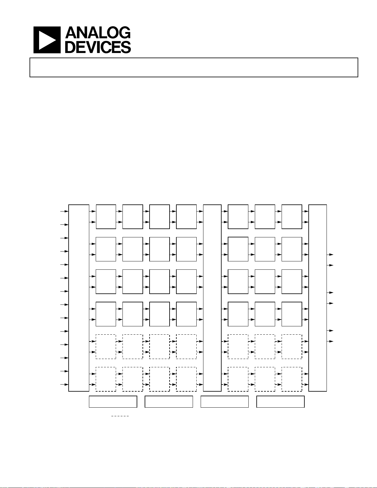
FUNCTIONAL BLOCK DIAGRAM
CLKA
ADC A/AI
NCO
CIC5
M = 1-32
FIR1
HB1
M = Byp, 2
FIR2
HB2
M = Byp, 2
Digital Down-Converter (DDC)
AD6636
6 programmable digital AGC loops with 96 dB range
Synchronous serial I/O operation (SPI®-, SPORT-compatible)
Supports 8-bit or 16-bit microport modes
3.3 V I/O, 1.8 V CMOS core
User-configurable built-in self-test (BIST) capability
JTAG boundary scan
APPLICATIONS
Multicarrier, multimode digital receivers
GSM, EDGE, PHS, UMTS, WCDMA, CDMA2000, TD-SCDMA
Micro and pico cell systems, software radios
Broadband data applications
Instrumentation and test equipment
Wireless local loop
In-building wireless telephony
MRCF
DRCF
M = 1-16
CRCF
M = 1-16
LHB
L = Byp, 2
EXPA [2:0]
CLKB
NCO
CIC5
M = 1-32
FIR1
HB1
M = Byp, 2
M = Byp, 2
INPUT MATRIX
ADC B/AQ
EXPB [2:0]
CMOS
CLKC
REAL
PORTS
CLKD
A, B,
C,D
CMOS
COMPLEX
PORTS
(AI, AQ)
(BI, BQ)
LVDS
PORTS
AB, CD
PEAK/
RMS
MEAS.
I,Q
CORR.
ADC C/CI
EXPC [2:0]
ADC D/CQ
EXPD [2:0]
______
RESET
SYNC [3:0]
NOTE: CHANNELS RENDERED AS
Rev. 0
Information furnished by Analog Devices is believed to be accurate and reliable.
However, no responsibility is assumed by Analog Devices for its use, nor for any
infringements of patents or other rights of third parties that may result from its use.
Specifications subject to change without notice. No license is granted by implication
or otherwise under any patent or patent rights of Analog Devices. Trademarks and
registered trademarks are the property of their respective owners.
NCO
NCO
NCO
NCO
MULTIPLIER
CIC5
M = 1-32
CIC5
M = 1-32
CIC5
M = 1-32
CIC5
M = 1-32
FIR1
HB1
M = Byp, 2
FIR1
HB1
M = Byp, 2
FIR1
HB1
M = Byp, 2
FIR1
HB1
M = Byp, 2
MICROPORT INTERFACE
M = Byp, 2
M = Byp, 2
M = Byp, 2
M = Byp, 2
16-BIT
FIR2
HB2
FIR2
HB2
FIR2
HB2
FIR2
HB2
FIR2
HB2
Figure 1.
MRCF
DRCF
M = 1-16
CRCF
M = 1-16
LHB
L = Byp, 2
DATA ROUTING
MRCF
DRCF
M = 1-16
MRCF
DRCF
M = 1-16
CRCF
M = 1-16
CRCF
M = 1-16
LHB
L = Byp, 2
LHB
L = Byp, 2
AGC
DATA ROUTER MATRIX
MRCF
DRCF
M = 1-16
CRCF
M = 1-16
LHB
L = Byp, 2
PARALLEL PORTS
MRCF
DRCF
M = 1-16
SPORT/SPI INTERFACE JTAGPLL CLOCK
M = DECIMATION L = INTERPOLATIONARE AVAILABLE ONLY IN 6-CHANNEL PART
CRCF
M = 1-16
LHB
L = Byp, 2
One Technology Way, P.O. Box 9106, Norwood, MA 02062-9106, U.S.A.
Tel: 781.329.4700
Fax: 781.326.8703 © 2004 Analog Devices, Inc. All rights reserved.
www.analog.com
PA
PB
PC
04998-0-001

AD6636
TABLE OF CONTENTS
Product Description......................................................................... 3
FIR Half-Band Block.................................................................. 29
Product Highlights....................................................................... 4
Specifications..................................................................................... 5
Electrical Characteristics ............................................................. 5
General Timing Characteristics ................................................. 6
Microport Timing Characteristics ............................................. 7
Serial Port Timing Characteristics............................................. 8
Explanation of Test Levels for Specifications............................ 8
Absolute Maximum Ratings............................................................ 9
Thermal Characteristics .............................................................. 9
ESD Caution.................................................................................. 9
Pin Configuration and Function Descriptions........................... 10
Pin Listing for Power, Ground, Data and Address Buses ......12
Timing Diagrams............................................................................ 13
Theory of Operation ...................................................................... 19
ADC Input Port .......................................................................... 19
Intermediate Data Router ......................................................... 32
Mono-Rate RAM Coefficient Filter (MRCF)......................... 32
Decimating RAM Coefficient Filter (DRCF) ........................ 33
Channel RAM Coefficient Filter (CRCF) ............................... 35
Interpolating Half-Band Filter.................................................. 36
Output Data Router................................................................... 37
Automatic Gain Control............................................................ 39
Parallel Port Output ................................................................... 43
User-Configurable Built-In Self-Test (BIST).......................... 47
Chip Synchronization................................................................ 47
Serial Port Control ..................................................................... 48
Microport .................................................................................... 52
JTAG Boundary Scan................................................................. 53
Memory Map .................................................................................. 54
Reading the Memory Map Table.............................................. 54
PLL Clock Multiplier .................................................................20
ADC Gain Control..................................................................... 21
ADC Input Port Monitor Function.......................................... 22
Quadrature I/Q Correction Block............................................ 24
Input Crossbar Matrix ............................................................... 26
Numerically Controlled Oscillator (NCO) ............................. 26
Fifth-Order CIC Filter ............................................................... 28
REVISION HISTORY
8/04—Revision 0: Initial Version
Global Register Map .................................................................. 56
Input Port Register Map............................................................ 59
Channel Register Map ............................................................... 62
Output Port Register Map......................................................... 67
Design Notes................................................................................... 70
Outline Dimensions....................................................................... 72
Ordering Guide .......................................................................... 72
Rev. 0 | Page 2 of 72

AD6636
PRODUCT DESCRIPTION
The AD6636 is a digital down-converter intended for IF
sampling or oversampled baseband radios requiring widebandwidth input signals. Optimized for the demanding filtering
requirements of wideband standards, such as CDMA2000,
UMTS, and TD-SCDMA, the AD6636 is designed for radio
systems that use either an IF sampling ADC or a baseband
sampling ADC.
The AD6636 channels have the following signal processing
stages: a frequency translator, a fifth-order cascaded integrated
comb filter, two sets of cascaded fixed-coefficient FIR and halfband filters, three cascaded programmable coefficient sum-ofproduct FIR filters, an interpolating half-band filter (IHB), and
a digital automatic gain control (AGC) block. Multiple modes
are supported for clocking data into and out of the chip and
provide flexibility for interfacing to a wide variety of digitizers.
Programming and control are accomplished via serial or
microport interfaces.
Input ports can take input data at up to 150 MSPS. Up to
300 MSPS input data can be supported using two input ports
(some external interface logic is required) and two internal
channels processing in tandem. Biphase filtering in output data
router is selected to complete the combined filtering mode. The
four input ports can operate in CMOS mode, or two ports can
be combined for LVDS input mode. The maximum input data
rate for each input port is 150 MHz.
Frequency translation is accomplished with a 32-bit complex
numerically controlled oscillator (NCO). It has greater than
110 dBc SDFR. This stage translates either a real or complex
input signal from IF (intermediate frequency) to a baseband
complex digital output. Phase and amplitude dither can be
enabled on-chip to improve spurious performance of the NCO.
A 16-bit phase-offset word is available to create a known phase
relationship between multiple AD6636 chips or channels. The
NCO also can be bypassed so that baseband I and Q inputs can
be provided directly from baseband sampling ADC through
input ports.
Following frequency translation is a fifth-order CIC filter with a
programmable decimation between 1 and 32. This filter is used
to lower the sample rate efficiently, while providing sufficient
alias rejection at frequencies with higher frequency offsets from
the signal of interest.
Following the CIC5 are two sets of filters. Each set has a nondecimating FIR filter and a decimate-by-2 half-band filter. The
FIR1 filter provides about 30 dB of rejection, while the HB1
filter provides about 77 dB of rejection. They can be used
together to achieve a 107 dB stopband alias rejection, or they
can be individually bypassed to save power. The FIR2 filter
provides about 30 dB of rejection, while the HB2 filter provides
about 65 dB of rejection. The filters can be used either together
to achieve more than 95 dB stopband alias rejection, or can be
individually bypassed to save power. FIR1 and HB1 filters can
run with a maximum input rate of 150 MSPS. In contrast, FIR2
and HB2 can run with a maximum input rate of 75 MSPS
(input rate to FIR2 and HB2 filters).
The programmable filtering is divided into three cascaded RAM
coefficient filters (RCFs) for flexible and power efficient
filtering. The first filter in the cascade is the MRCF, consisting
of a programmable nondecimating FIR. It is followed by
programmable FIR filters (DRCF) with decimation from 1
to 16. They can be used either together to provide high rejection
filters, or independently to save power. The maximum input rate
to the MRCF is one-fourth of PLL clock rate.
The CRCF (Channel RCF) is the last programmable FIR filter
with programmable decimation from 1 to 16. It typically is used
to meet the spectral mask requirements for the air standard of
interest. This could be an RRC, anti-aliasing filter or any other
real data filter. Decimation in preceding blocks is used to keep
the input rate of this stage as low as possible for the best filter
performance.
The last filter stage in the chain is an interpolate-by-2 half-band
filter, which is used to up-sample the CRCF output to produce
higher output oversampling. Signal rejection requirements for
this stage are relaxed because preceding filters already have
filtered the blockers and adjacent carriers.
Each input port of the AD6636 has its own clock used for
latching onto the input data, but Input Port A clock (CLKA) is
used also as the input for an on-board PLL clock multiplier. The
output of the PLL clock is used for processing all filters and
processing blocks beyond the data router following CIC filter.
The PLL clock can be programmed to have a maximum clock
rate of 200 MHz.
A data routing block (DR) is used to distribute data from the
CICs to the various channel filters. This block allows multiple
back end filter chains to work together to process high
bandwidth signals or to make even sharper filter transitions
than a single channel can perform. It also can allow complex
filtering operations to be achieved in the programmable filters.
The digital AGC provides the user with scaled digital outputs
based on the rms level of the signal present at the output of the
digital filters. The user can set the requested level and time
constant of the AGC loop for optimum performance of the
postprocessor. This is a critical function in the base station for
CDMA applications where the power level must be well
controlled going into the RAKE receivers. It has programmable
clipping and rounding control to provide different output
resolutions.
Rev. 0 | Page 3 of 72

AD6636
The overall filter response for the AD6636 is the composite of
all the combined filter stages. Each successive filter stage is
capable of narrower transition bandwidths, but requires a
greater number of CLK cycles to calculate the output. More
decimation in the first filter stage minimizes overall power
consumption. Data from the device is interfaced to a
DSP/FPGA/baseband processor via either high speed parallel
ports (preferred) or a DSP-compatible microprocessor interface.
The AD6636 is available both in 4-channel and 6-channel
versions. The data sheet primarily discusses the 6-channel part.
The only difference between the 6-channel and 4-channel
devices is that on the 4-channel version, Channels 4 and 5 are
not available (see Figure 1). The 4-channel device still has the
same input ports, output ports, and memory map. The memory
map section for Channels 4 and 5 can be programmed and read
back, but it serves no purpose.
PRODUCT HIGHLIGHTS
• Six independent digital filtering channels
• 101 dB SNR noise performance, 110 dB spurious
performance
• Four input ports capable of 150 MSPS input data rates
• RMS/peak power monitoring of input ports and 96 dB
range AGCs before the output ports
• Three programmable RAM coefficient filters, three half-
band filters, two fixed coefficient filters, and one fifth-order
CIC filter per channel
• Complex filtering and biphase filtering (300 MSPS ADC
input) by combining filtering capability of multiple
channels
• Three 16-bit parallel output ports operating at up to
200 MHz clock
• Blackfin®- and TigerSHARC®-compatible 16-bit
microprocessor port
• Synchronous serial communications port is compatible
with most serial interface standards, SPORT, SPI, and SSR
Rev. 0 | Page 4 of 72

AD6636
SPECIFICATIONS
Table 1. Recommended Operating Conditions
Parameter Temp Test Level Min Typ Max Unit
VDDCORE Full IV 1.7 1.8 1.9 V
VDDIO Full IV 3.0 3.3 3.6 V
T
Full IV −40 +25 +85 °C
AMBIENT
ELECTRICAL CHARACTERISTICS
Table 2. Electrical Characteristics1
Parameter Temp Test Level Min Typ Max Unit
LOGIC INPUTS (NOT 5 V TOLERANT)
Logic Compatibility Full IV 3.3 V CMOS
Logic 1 Voltage Full IV 2.0 3.6 V
Logic 0 Voltage Full IV −0.3 +0.8 V
Logic 1 Current Full IV 1 10 µA
Logic 0 Current Full IV 1 10 µA
Input Capacitance 25°C V 4 pF
LOGIC OUTPUTS
Logic Compatibility Full IV 3.3 V CMOS
Logic 1 Voltage (IOH = 0.25 mA) Full IV 2.0 VDDIO − 0.2 V
Logic 0 Voltage (IOL = 0.25 mA) Full IV 0.2 0.4 V
SUPPLY CURRENTS
WCDMA (61.44 MHz) Example1
I
25°C V 450 mA
VDDCORE
I
25°C V 50 mA
VDDIO
CDMA 2000 (61.44 MHz) Example1 25°C V
I
25°C V 400 mA
VDDCORE
I
25°C V 25 mA
VDDIO
TDS-CDMA (76.8 MHz) Example
I
25°C V 250 mA
VDDCORE
I
25°C V 15 mA
VDDIO
GSM (65 MHz) Example
I
25°C V 175 mA
VDDCORE
I
25°C V 10 mA
VDDIO
1, 2
TOTAL POWER DISSIPATION
WCDMA (61.44 MHz)1 25°C V 975 mW
CDMA 2000 (61.44 MHz)1 25°C V 800 mW
TDS-CDMA, (76.8 MHz)
GSM, (65 MHz)
1, 2
1, 2
25°C V 350 mW
1
One input port, all six channels, and the relevant signal processing blocks are active.
2
PLL is turned off for power savings.
1, 2
25°C V 500 mW
Rev. 0 | Page 5 of 72

AD6636
GENERAL TIMING CHARACTERISTICS
Table 3. General Timing Characteristics
Parameter Temp Test Level Min Typ Max Unit
CLK TIMING REQUIREMENTS
t
CLKx Period (x = A, B, C, D) Full I 6.66 ns
CLK
t
CLKx Width Low (x = A, B, C, D) Full IV 1.71 0.5 × t
CLKL
t
CLKx Width High (x = A, B, C, D) Full IV 1.70 0.5 × t
CLKH
t
CLKA to CLKx Skew (x = B, C, D) Full IV t
CLKSKEW
INPUT WIDEBAND DATA TIMING REQUIREMENTS Full IV
tSI
tHI
t
t
t
SEXP
HEXP
DEXP
INx [15:0] to ↑CLKx Setup Time (x = A, B, C, D)
INx [15:0] to ↑CLKx Hold Time (x = A, B, C, D)
EXPx [2:0] to ↑CLKx Setup Time (x = A, B, C, D)
EXPx [2:0] to ↑CLKx Hold Time (x = A, B, C, D)
↑CLKx to EXPx[2:0] Delay (x = A, B, C, D)
PARALLEL OUTPUT PORT TIMING REQUIREMENTS (MASTER)
t
DPREQ
t
DPP
t
DPIQ
t
DPCH
t
DPGAIN
t
SPA
t
HPA
↑PCLK to ↑Px REQ Delay (x = A, B, C)
↑PCLK to Px [15:0] Delay (x = A, B, C)
↑PCLK to Px IQ Delay (x = A, B, C)
↑PCLK to Px CH[2:0] Delay (x = A, B, C)
↑PCLK to Px Gain Delay (x = A, B, C)
Px ACK to ↑PCLK Setup Time (x = A, B, C)
Px ACK to ↑PCLK Hold Time (x = A, B, C)
PARALLEL OUTPUT PORT TIMING REQUIREMENTS (SLAVE)
t
PCLK Period Full IV 5.0 ns
PCLK
t
PCLK Low Period Full IV 1.7 0.5 × t
PCLKL
t
PCLK High Period Full IV 0.7 0.5 × t
PCLKH
t
DPREQ
t
DPP
t
DPIQ
t
DPCH
t
DPGAIN
t
SPA
t
HPA
↑PCLK to ↑Px REQ Delay (x = A, B, C)
↑PCLK to Px [15:0] Delay (x = A, B, C)
↑PCLK to Px IQ Delay (x = A, B, C)
↑PCLK to Px CH[2:0] Delay (x = A, B, C)
↑PCLK to Px Gain Delay (x = A, B, C)
Px ACK to ↓PCLK Setup Time (x = A, B, C)
Px ACK to ↓PCLK Hold Time (x = A, B, C)
MISC PINS TIMING REQUIREMENTS
t
RESET
t
DIRP
tSS
tHS
RESET Width Low
CPUCLK/SCLK to
IRP Delay
SYNC(0, 1, 2, 3) to ↑CLKA Setup Time
SYNC(0, 1, 2, 3) to ↑CLKA Hold Time
1
All timing specifications are valid over the VDDCORE range of 1.7 V to 1.9 V and the VDDIO range of 3.0 V to 3.6 V.
2
C
= 40 pF on all outputs, unless otherwise noted.
LOAD
1, 2
ns
CLK
ns
CLK
− 1.3 ns
CLK
Full IV 0.75 ns
Full IV 1.13 ns
Full IV 3.37 ns
Full IV 1.11 ns
Full IV 5.98 10.74 ns
Full IV 1.77 3.86 ns
Full IV 2.07 5.29 ns
Full IV 0.48 5.49 ns
Full IV 0.38 5.35 ns
Full IV 0.23 4.95 ns
Full IV 4.59 ns
Full IV 0.90 ns
ns
PCLK
ns
PCLK
Full IV 4.72 8.87 ns
Full IV 4.8 8.48 ns
Full IV 4.83 10.94 ns
Full IV 4.88 10.09 ns
Full IV 5.08 11.49 ns
Full IV 6.09 ns
Full IV 1.0 ns
Full IV 30 ns
Full V 7.5 ns
Full IV 0.87 ns
Full IV 0.67 ns
Rev. 0 | Page 6 of 72

AD6636
MICROPORT TIMING CHARACTERISTICS
Table 4. Microport Timing Characteristics
Parameter Temp Test Level Min Typ Max Unit
MICROPORT CLOCK TIMING REQUIREMENTS
t
CPUCLK Period Full IV 10.0 ns
CPUCLK
t
CPUCLK Low Time Full IV 1.53 0.5 × t
CPUCLKL
t
CPUCLK High Time Full IV 1.70 0.5 × t
CPUCLKH
INM MODE WRITE TIMING (MODE = 0)
tSC
tHC
t
SAM
t
HAM
t
DRDY
t
Write Access Time Full IV 3 × t
ACC
3
Control
Control
to ↑CPUCLK Setup Time
3
to ↑CPUCLK Hold Time
Address/Data to ↑CPUCLK Setup Time
Address/Data to ↑CPUCLK Hold Time
↑CPUCLK to RDY (
DTACK) Delay
INM MODE READ TIMING (MODE = 0)
tSC
tHC
t
SAM
t
HAM
tDD
t
DRDY
t
Read Access Time Full IV 3 × t
ACC
3
Control
Control
to ↑CPUCLK Setup Time
3
to ↑CPUCLK Hold Time
Address to ↑CPUCLK Setup Time
Address to ↑CPUCLK Hold Time
↑CPUCLK to Data Delay
↑CPUCLK to RDY (
DTACK) Delay
MNM MODE WRITE TIMING (MODE = 1)
tSC
tHC
t
SAM
t
HAM
t
DDTACK
t
Write Access Time Full IV 3 × t
ACC
3
Control
Control
to ↑CPUCLK Setup Time
3
to ↑CPUCLK Hold Time
Address/Data to ↑CPUCLK Setup Time
Address/Data to ↑CPUCLK Hold Time
↑CPUCLK to
DTACK (RDY) Delay
MNM MODE READ TIMING (MODE = 1)
tSC
tHC
t
SAM
t
HAM
3
Control
Control
to ↑CPUCLK Setup Time
3
to ↑CPUCLK Hold Time
Address to ↑CPUCLK Setup Time
Address to ↑CPUCLK Hold Time
tDD CPUCLK to Data Delay Full V 5.0 ns
t
DDTACK
t
ACC
↑CPUCLK to
Read Access Time Full IV 3 × t
DTACK (RDY) Delay
1
All timing specifications are valid over the VDDCORE range of 1.7 V to 1.9 V and the VDDIO range of 3.0 V to 3.6 V.
2
C
= 40 pF on all outputs, unless otherwise noted.
LOAD
3
Specification pertains to control signals: R/W (WR), DS (RD), and CS.
1, 2
ns
CPUCLK
ns
CPUCLK
Full IV 0.80 ns
Full IV 0.09 ns
Full IV 0.76 ns
Full IV 0.20 ns
Full IV 3.51 6.72 ns
9 × t
CPUCLK
CPUCLK
ns
Full IV 1.00 ns
Full IV 0.03 ns
Full IV 0.80 ns
Full IV 0.20 ns
Full V 5.0 ns
Full IV 4.50 6.72 ns
9 × t
CPUCLK
CPUCLK
ns
Full IV 1.00 ns
Full IV 0.00 ns
Full IV 0.00 ns
Full IV 0.57 ns
Full IV 4.10 5.72 ns
9 × t
CPUCLK
CPUCLK
ns
Full IV 1.00 ns
Full IV 0.00 ns
Full IV 0.00 ns
Full IV 0.57 ns
Full IV 4.20 6.03 ns
9 × t
CPUCLK
CPUCLK
ns
Rev. 0 | Page 7 of 72

AD6636
SERIAL PORT TIMING CHARACTERISTICS
Table 5. Serial Port Timing Characteristics
Parameter Temp Test Level Min Typ Max Unit
SERIAL PORT CLOCK TIMING REQUIREMENTS
t
SCLK Period Full IV 10.0 ns
SCLK
t
SCLK Low Time Full IV 1.60 0.5 × t
SCLKL
t
SCLK High Time Full IV 1.60 0.5 × t
SCLKH
SPI PORT CONTROL TIMING REQUIREMENTS (MODE = 0)
t
SSI
t
HSI
t
SSCS
t
HSCS
t
DSDO
SDI to ↓SCLK Setup Time
SDI to ↓SCLK Hold Time
SCS to ↑SCLK Setup Time
SCS to ↑SCLK Hold Time
↑SCLK to SDO Delay Time
SPORT MODE CONTROL TIMING REQUIREMENTS (MODE = 1)
t
SSI
t
HSI
t
SSRFS
t
HSRFS
t
SSTFS
t
HSTFS
t
SSCS
t
HSCS
t
DSDO
SDI to ↓SCLK Setup Time
SDI to ↓SCLK Hold Time
SRFS to ↓SCLK Setup Time
SRFS to ↓SCLK Hold Time
STFS to ↑SCLK Setup Time
STFS to ↑SCLK Hold Time
SCS to ↑SCLK Setup Time
SCS to ↑SCLK Hold Time
↑SCLK to SDO Delay Time
1
All timing specifications are valid over the VDDCORE range of 1.7 V to 1.9 V and the VDDIO range of 3.0 V to 3.6 V.
2
C
= 40 pF on all outputs, unless otherwise noted.
LOAD
1, 2
ns
SCLK
ns
SCLK
Full IV 1.30 ns
Full IV 0.40 ns
Full IV 4.12 ns
Full IV −2.78 ns
Full IV 4.28 7.96 ns
Full IV 0.80 ns
Full IV 0.40 ns
Full IV 1.60 ns
Full IV −0.13 ns
Full IV 1.60 ns
Full IV −0.30 ns
Full IV 4.12 ns
Full IV −2.76 ns
Full IV 4.29 7.95 ns
EXPLANATION OF TEST LEVELS FOR SPECIFICATIONS
I 100% production tested.
II 100% production tested at 25°C, and sample tested at specified temperatures.
III Sample tested only.
IV Parameter guaranteed by design and analysis.
V Parameter is typical value only.
VI 100% production tested at 25°C, and sampled tested at temperature extremes.
Rev. 0 | Page 8 of 72

AD6636
ABSOLUTE MAXIMUM RATINGS
Table 6.
Parameter Rating
ELECTRICAL
VDDCORE Supply Voltage
(Core Supply)
VDDIO Supply Voltage
(Ring or IO Supply)
Input Voltage −0.3 to +3.6 V (not 5 V tolerant)
Output Voltage −0.3 to VDDIO + 0.3 V
Load Capacitance 200 pF
ENVIRONMENTAL
Operating Temperature
Range (Ambient)
Maximum Junction
Temperature under Bias
Storage Temperature Range
(Ambient)
2.2 V
4.0 V
−40°C to +85°C
125°C
−65°C to +150°C
Stresses above those listed under the Absolute Maximum
Ratings may cause permanent damage to the device. This is a
stress rating only; functional operation of the device at these or
any other conditions above those indicated in the operational
section of this specification is not implied. Exposure to absolute
maximum rating conditions for extended periods may affect
device reliability.
THERMAL CHARACTERISTICS
256-ball CSP_BGA package:
= 25.4°C /W, no airflow
θ
JA
= 23.3°C /W, 0.5 m/s airflow
θ
JA
= 22.6°C /W, 1.0 m/s airflow
θ
JA
= 21.9°C /W, 2.0 m/s airflow
θ
JA
Thermal measurements made in the horizontal position on a
4-layer board with vias.
ESD CAUTION
ESD (electrostatic discharge) sensitive device. Electrostatic charges as high as 4000 V readily accumulate on
the human body and test equipment and can discharge without detection. Although this product features
proprietary ESD protection circuitry, permanent damage may occur on devices subjected to high energy
electrostatic discharges. Therefore, proper ESD precautions are recommended to avoid performance
degradation or loss of functionality.
Rev. 0 | Page 9 of 72
AD6636
PIN CONFIGURATION AND FUNCTION DESCRIPTIONS
12345678910111213141516
GND INC3 IND4 IND7 CLKD CLKC IND11 GND VDDCORE IND14 IND15 SYNC1 TDO PBGAIN PB11 GND
A
IND0 VDDIO INC2 IND5 IND6 IND8 IND10 IND12 IND13 INC14 SYNC3 SYNC0 TRST PBCH2 VDDIO PB12
B
EXPA1 EXPD1 INC0 INC1 IND3 INC5 IND9 INC10 INC13 SYNC2 TMS TCLK PBCH0 PB8 PB15 PB10
C
EXPB0 EXPC2 EXPC1 EXPD0 IND2 INC4 INC7 INC9 INC12 TDI PBCH1 PBIQ PB14 PB9 PB13 PACH1
D
INA14 INA15 EXPA0 LVDS_RSET GND IND1 INC6 INC8 INC11 INC15 PBREQ PBACK PB4 PB5 PB1 PCLK
E
INA12 INA13 EXPB1 EXPC0 EXPD2 GND VDDIO VDDIO VDDIO VDDIO GND PB6 PB0 PB7 PAREQ PA0
F
A
B
C
D
E
F
INA11 INB13 INB15 EXPB2 EXPA2 VDDCORE GND GND GND GND VDDCORE PB3 PAGAIN PB2 PACH0 PA2
G
VDDCORE INA10 INB12 INB11 INB14 VDDCORE GND GND GND GND VDDCORE PACH2 PAIQ PAACK PA1 GND
H
GND INA9 INB10 INB8 INB9 VDDCORE GND GND GND GND VDDCORE PA3 PA7 PA5 PA4 VDDCORE
J
CLKA INA8 INA7 INB6 INB7 VDDCORE GND GND GND GND VDDCORE PA12 PA15 PA9 PA8 PA6
K
CLKB INA6 INB4 INB1 INB3 GND VDDIO VDDIO VDDIO VDDIO GND PC3 PCACK PCCH1 PA13 PA10
L
INA5 INB5 INB2 INB0 GND D13 D15 D5 A5 PC12 PC7 PC2 PC0 PCCH0 PA11
M
RESET
MSB_
FIRST
R/W (WR,
CS (SCS)
STFS)
DS (RD,
SRFS)
EXT_
CHIPID1 D14 D10 D11 D6 D0 A3 A1 PC9 PC6 VDDIO PCREQ
FILTER
INA4 INA3 INA0 CHIPID2 D12 D2 D1 A4 A0 (SDI) PC15 PC5 PC1 PCCH2 PA14
N
INA2 INA1 SMODE CHIPID3 GND D9 D4 A6 A2 PC11 PC10 PC4 PCIQ PCGAIN
P
R
T
CPUCLK
VDDIO
(SCLK)
GND MODE CHIPID0 D7 D8 D3 VDDCORE GND GND A7 PC14 PC13 PC8 GND GND
IRP
12345678910111213141516
DTACK
(RDY, SDO)
= VDDCORE = VDDIO = GROUND
G
H
J
K
L
M
N
P
R
T
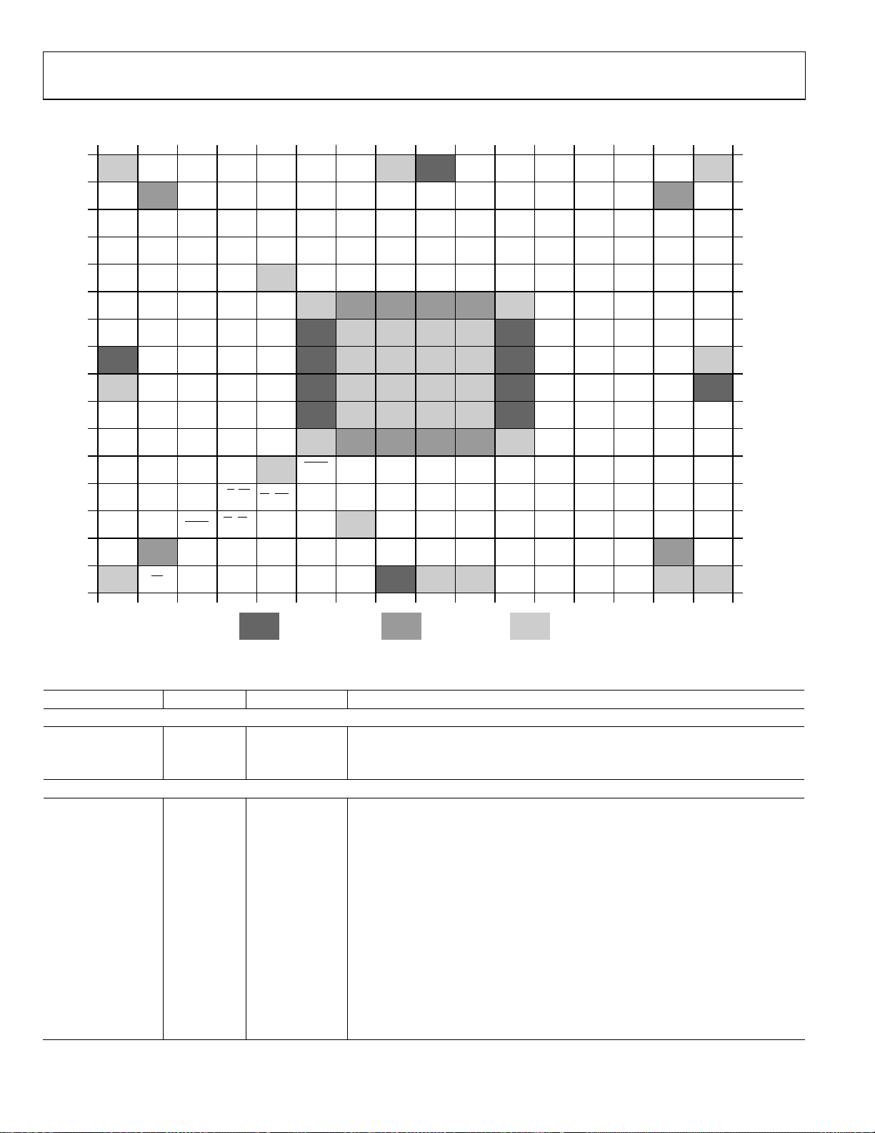
Figure 2. CSP_BGA Pin Configuration
Table 7. Pin Names and Functions
Name Type Pin No. Function
POWER SUPPLY
VDDCORE Power See Table 8 1.8 V Digital Core Supply.
VDDIO Power See Table 8 3.3 V Digital I/O Supply.
GND Ground See Table 8 Digital Core and I/O Ground.
INPUT (ADC) PORTS (CMOS/LVDS)
CLKA Input K1
Clock for Input Port A. Used to clock INA[15:0] and EXPA[2:0] data. Additionally,
this clock is used to drive internal circuitry and PLL clock multiplier.
CLKB Input L1 Clock for Input Port B. Used to clock INB[15:0] and EXPB[2:0] data.
CLKC Input A6 Clock for Input Port C. Used to clock INC[15:0] and EXPC[2:0] data.
CLKD Input A5 Clock for Input Port D. Used to clock IND[15:0] and EXPD[2:0] data.
INA[0:15] Input See Table 8 Input Port A (Parallel).
INB[0:15] Input See Table 8 Input Port B (Parallel).
INC[0:15] Input See Table 8 Input Port C (Parallel).
IND[0:15] Input See Table 8 Input Port D (Parallel).
EXPA[0:2] Bidirectional E3, C1, G5 Exponent Bus Input Port A. Gain control output.
EXPB[0:2] Bidirectional D1, F3, G4 Exponent Bus Input Port B. Gain control output.
EXPC[0:2] Bidirectional F4, D3, D2 Exponent Bus Input Port C. Gain control output.
EXPD[0:2] Bidirectional D4, C2, F5 Exponent Bus Input Port D. Gain control output.
CLKA, CLKB Input K1, L1 LVDS Differential Clock for LVDS_A Input Port (LVDS_CLKA+, LVDS_CLKA−).
04998-0-002
Rev. 0 | Page 10 of 72

AD6636
Name Type Pin No. Function
CLKC, CLKD Input A6, A5 LVDS Differential Clock for LVDS_C Input Port (LVDS_CLKC+, LVDS_CLKC−).
INA[0:15], INB[0:15] LVDS Input See Table 8
INC[0:15], IND[0:15] LVDS Input See Table 8
OUTPUT PORTS
PCLK Bidirectional E16 Parallel Output Port Clock. Master mode output, Slave mode input.
PA[0:15] Output See Table 8 Parallel Output Port A Data Bus.
PACH[0:2] Output G15, D16, H12 Channel Indicator Output Port A.
PAIQ Output H13 Parallel Port A I/Q Data Indicator. Logic 1 indicates I data on data bus.
PAGAIN Output G13
PAACK Input H14 Parallel Port A Acknowledge (Active High).
PAREQ Output F15 Parallel Port A Request (Active High).
PB[0:15] Output See Table 8 Parallel Output Port B Data Bus.
PBCH[0:2] Output C13, D11, B14 Channel Indicator Output Port B.
PBIQ Output D12 Parallel Port B I/Q Data Indicator. Logic 1 indicates I data on data bus.
PBGAIN Output A14
PBACK Input E12 Parallel Port B Acknowledge (Active High).
PBREQ Output E11 Parallel Port B Request (Active High).
PC[0:15] Output See Table 8 Parallel Output Port C Data Bus.
PCCH[0:2] Output M15, L14, N15 Channel Indicator Output Port C.
PCIQ Output P15 Parallel Port C I/Q Data Indicator. Logic 1 indicates I data on data bus.
PCGAIN Output P16
PCACK Input L13 Parallel Port C Acknowledge (Active High).
PCREQ Output R16 Parallel Port C Request (Active High).
MISC PINS
RESET
IRP
SYNC[0:3] Input
LVDS_RSET Input E4 LVDS Resistor Set Pin (Analog Pin). See Design Notes.
EXT_FILTER Input R4 PLL Loop Filter (Analog Pin). See Design Notes.
MICROPORT CONTROL
D[0:15] Bidirectional See Table 8
A[0:7] Input See Table 8 Microport Address Bus.
DS(RD)
DTACK (RDY)1
R/W (WR)
MODE Input T3 Mode Select Pin.
CS
CPUCLK Input R1 Microport CLK Input (Input Only).
CHIPID[0:3] Input T4, R5, N6, P6 Chip ID Input Pins.
Input P3 Master Reset (Active Low).
Output T2 Interrupt Pin.
B12, A12, C10,
B11
Input P4 Active Low Data Strobe when MODE = 1.
Output M6 Active Low Data Acknowledge when MODE = 1.
Input N4 Read/Write Strobe when MODE = 1.
Input N5 Active Low Chip Select. Logic 1 three-states the microport data bus.
In LVDS input mode, INA[0 :15] and INB[0 :15] form a differential pair
LVDS_A+[0:15] (positive node) and LVDS_A–[0:15] (negative node), respectively.
In LVDS input mode, INC[0 :15] and IND[0 :15] form a differential pair
LVDS_C+[0:15] (positive node) and LVDS_C–[0:15] (negative node), respectively.
Parallel Port A Gain Word Output Indicator. Logic 1 indicates gain word on
data bus.
Parallel Port B Gain Word Output Indicator. Logic 1 indicates gain word on
data bus.
Parallel Port C Gain Word Output Indicator. Logic 1 indicates gain word on
data bus.
Synchronization Inputs. SYNC pins are independent of channels or input ports and
independent of each other.
CS
Bidirectional Microport Data. This bus is three-stated when
Active Low Read Strobe when MODE = 0.
Microport Status Pin when MODE = 0.
Active Low Write Strobe when MODE = 0.
When SMODE = 0: Logic 0 = Intel mode; Logic 1 = Motorola mode.
When SMODE = 1: Logic 0 = SPI mode; Logic 1 = SPORT mode.
is high.
Rev. 0 | Page 11 of 72

AD6636
Name Type Pin No. Function
SERIAL PORT CONTROL
SCLK Input R1 Serial Clock.
SDO Output M6 Serial Port Data Output.
SDI2 Input N11 Serial Port Data Input.
STFS Input N4 Serial Transmit Frame Sync.
SRFS Input P4 Serial Receive Frame Sync.
SCS
MSB_FIRST Input R3
SMODE Input P5
JTAG
TRST1
TCLK2 Input C12 Test Clock.
TMS1 Input C11 Test Mode Select.
TDO Output A13 Test Data Output. Three-stated when JTAG is in reset.
TDI1 Input D10 Test Data Input.
1
Pin with a pull-up resistor of nominal 70 kΩ.
2
Pin with a pull-down resistor of nominal 70 kΩ.
Input N5 Serial Chip Select.
Select MSB First into SDI Pin and MSB First Out of SDO Pin. Logic 0 = MSB first;
Logic 1 = LSB first.
Serial Mode Select. Pull high when serial port is used and low when microport is
used.
Input B13 Test Reset Pin. Pull low when JTAG is not used.
PIN LISTING FOR POWER, GROUND, DATA AND ADDRESS BUSES
Table 8.
Name Pin No.
VDDCORE A9, G6, G11, H1, H6, H11, J6, J11, J16, K6, K11, T8
VDDIO B2, B15, F7, F8, F9, F10, L7, L8, L9, L10, R2, R15
GND
INA[0:15] N3, P2, P1, N2, N1, M1, L2, K3, K2, J2, H2, G1, F1, F2, E1, E2
INB[0:15] M4, L4, M3, L5, L3, M2, K4, K5, J4, J5, J3, H4, H3, G2, H5, G3
INC[0:15] C3, C4, B3, A2, D6, C6, E7, D7, E8, D8, C8, E9, D9, C9, B10, E10
IND[0:15] B1, E6, D5, C5, A3, B4, B5, A4, B6, C7, B7, A7, B8, B9, A10, A11
PA[0:15] F16, H15, G16, J12, J15, J14, K16, J13, K15, K14, L16, M16, K12, L15, N16, K13
PB[0:15] F13, E15, G14, G12, E13, E14, F12, F14, C14, D14, C16, A15, B16, D15, D13, C15
PC[0:15] M14, N14, M13, L12, P14, N13, R14, M12, T14, R13, P13, P12, M11, T13, T12, N12
D[0:15] R10, N9, N8, T7, P9, M9, R9, T5, T6, P8, R7, R8, N7, M7, R6, M8
A[0:7] N11, R12, P11, R11, N10, M10, P10, T11
A1, A8, A16, E5, F6, F11, G7, G8, G9, G10, H7, H8, H9, H10, H16, J1, J7, J8, J9, J10, K7, K8, K9, K10, L6, L11, M5,
P7, T1, T9, T10, T15, T16
Rev. 0 | Page 12 of 72
AD6636
CLKx
A
S
TIMING DIAGRAMS
RESET
t
RESL
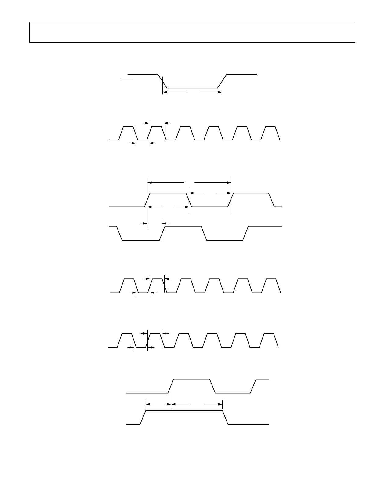
Figure 3. Reset Timing Requirements
t
CLKH
t
CLKL
Figure 4. CLK Switching Characteristics
(x = A, B, C, D for Individual Input Ports)
t
CLK
t
CLKL
CLK
t
CLKH
04998-0-003
04998-0-004
t
CLKSKEW
CLKx
04998-0-005
Figure 5. CLK Skew Characteristics
(x = B, C, D for Individual Input Ports)
t
CPUCLKH
CPUCLK
t
CPUCLKL
04998-0-006
Figure 6. CPUCLK Switching Characteristics
t
SCLKH
SCLK
t
SCLKL
04998-0-007
Figure 7. SCLK Switching Characteristics
CLKA
t
HSYNC
04998-0-008
YNC [3:0]
t
SSYNC
Figure 8. SYNC Tim ing Inputs
Rev. 0 | Page 13 of 72
AD6636
CLKx
EXPx[2:0]
t
CLK
t
CLKL
t
CLKH
t
DEXP
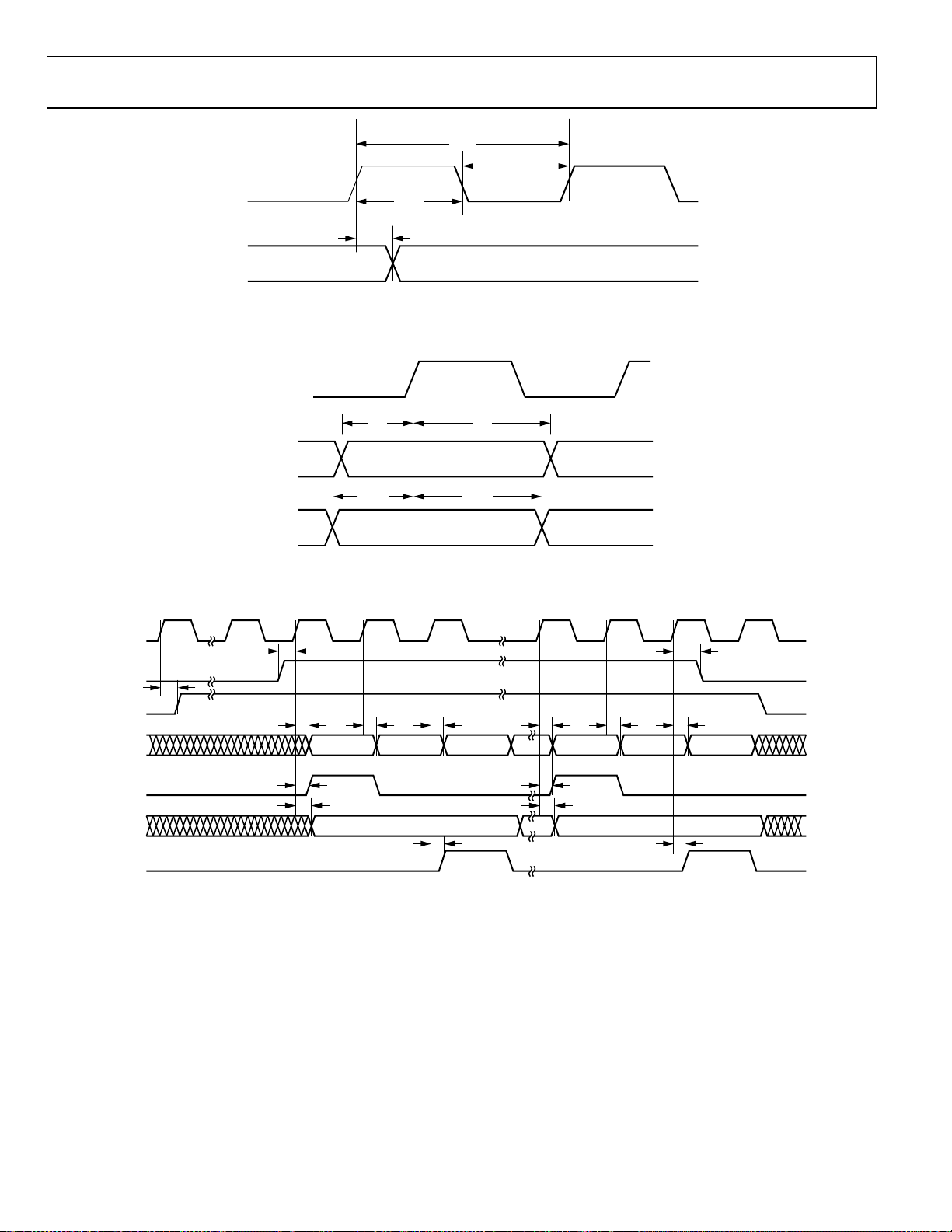
Figure 9. Gain Control Word Output Switching Characteristics
(x = A, B, C, D for Individual Input Ports)
CLKx
04998-0-009
t
HEXP
t
HI
04998-0-010
INx[15:0]
EXPx[15:0]
t
t
SEXP
SI
Figure 10. Input Port Timing for Data
(x = A, B, C, D for Individual Input Ports)
PCLK
PxACK
t
DPREQ
PxREQ
Px [15:0]
PxIQ
PxCH [2:0]
PxGAIN
t
SPA
t
DPP
I [15:0] Q [15:0]
t
DPIQ
t
DPCH
t
DPP
RSSI [11:0]
PxCH [2:0] = CHANNEL #
t
DPGAIN
t
t
DPP
DPP
I [15:0] Q [15:0]
t
DPIQ
t
DPCH
PxCH [2:0] = CHANNEL #
t
DPGAIN
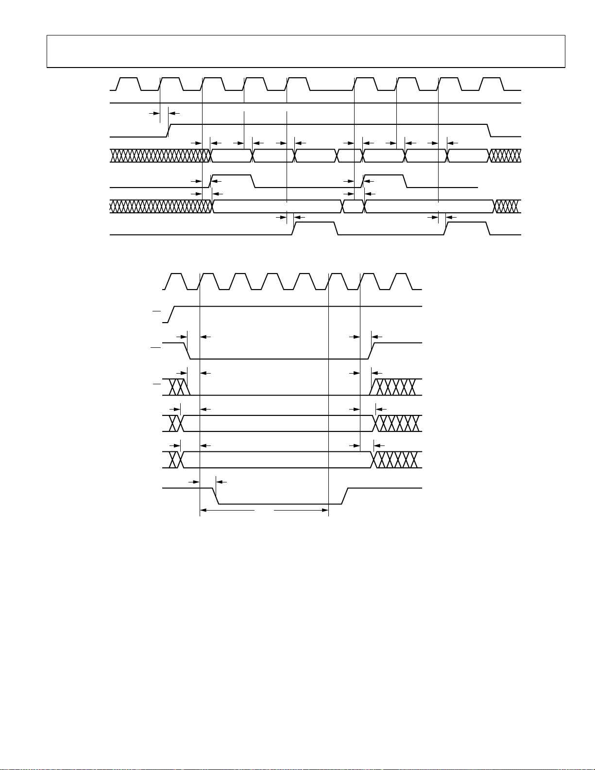
Figure 11. Master Mode PxACK to PCLK Switching Characteristics
(x = A, B, C, D for Individual Output Ports)
t
HPA
t
DPP
t
DPP
RSSI [11:0]
04998-0-011
Rev. 0 | Page 14 of 72
AD6636
PCLK
PxACK
PxREQ
Px [15:0]
PxIQ
PxCH [2:0]
PxGAIN
t
t
DPIQ
DPREQ
TIED LOGIC HIGH ALL THE TIME
t
DPP
I [15:0] Q [15:0]
t
DPCH
t
DPP
PxCH [2:0] = CHANNEL #
t
DPGAIN
t
DPP
RSSI [11:0] RSSI [11:0]
t
DPP
I [15:0] Q [15:0]
t
DPIQ
t
DPCH
t
DPP
PxCH [2:0] = CHANNEL #
t
DPGAIN
t
DPP
04998-0-012
Figure 12. Master Mode PxREQ to PCLK Switching Characteristics
CPUCLK
RD
WR
CS
t
SC
t
SC
t
HC
t
HC
t
SAM
A [7:0]
t
SAM
D [15:0]
RDY
NOTE:
t
ACCESS TIME DEPENDS ON THE ADDRESS ACCESSED. IT CAN VARY FROM 3 TO 9 CPUCLK CYCLES.
ACC
t
DRDY
VALID ADDRESS
VALID DATA
t
ACC
t
HAM
t
HAM
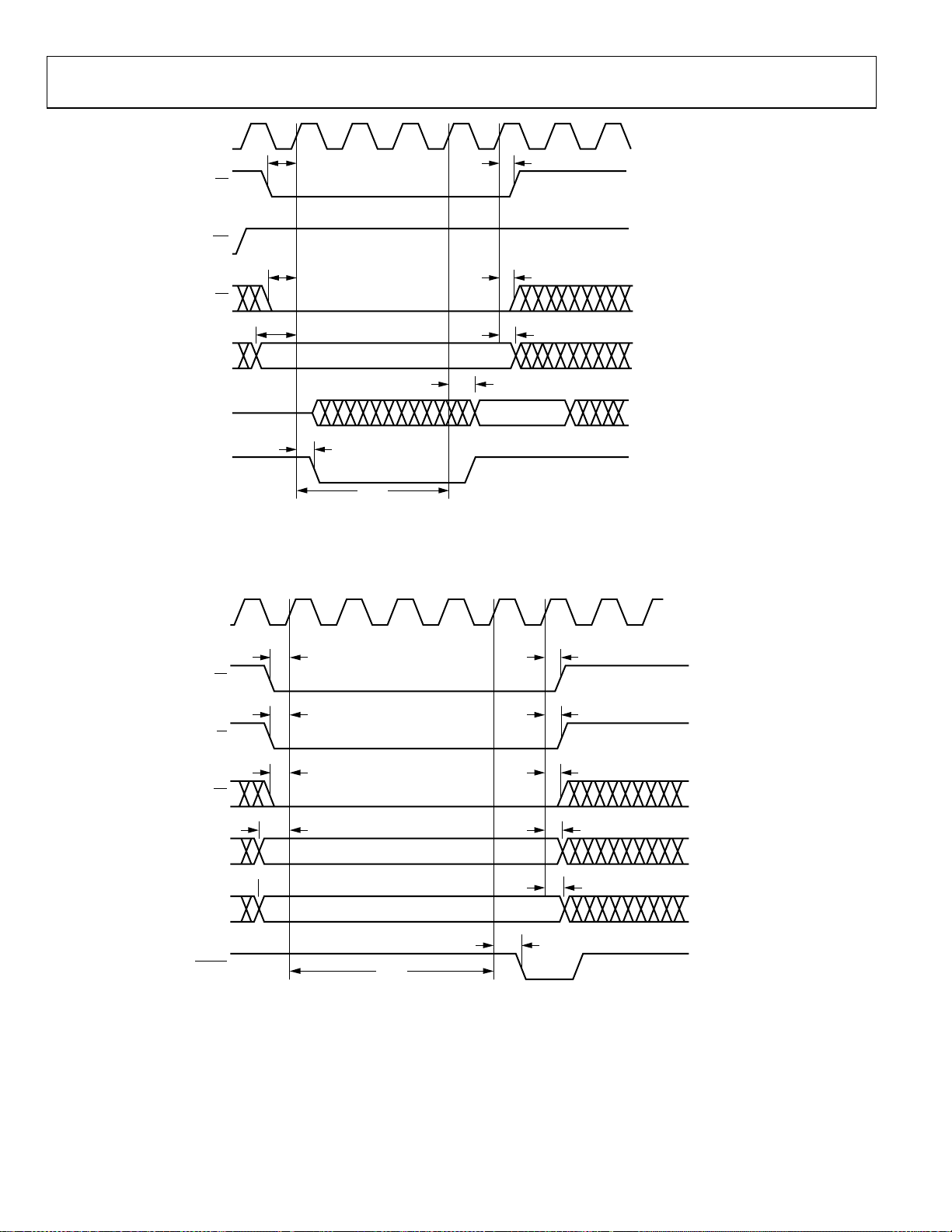
Figure 13. INM Microport Write Timing Requirements
04998-0-013
Rev. 0 | Page 15 of 72
AD6636
K
CPUCLK
RD
WR
CS
A [7:0]
t
SAM
t
t
SC
t
SC
VALID ADDRESS
HC
t
HC
t
HAM
t
DD
D [15:0]
t
DRDY
RDY
t
ACC
NOTE:
t
ACCESS TIME DEPENDS ON THE ADDRESS ACCESSED. IT CAN VARY FROM 3 TO 9 CPUCLK CYCLES.
ACC
VALID DATA
04998-0-014
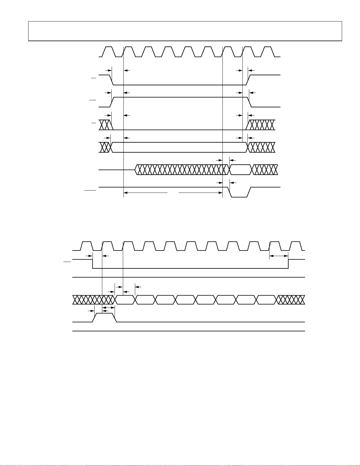
Figure 14. INM Microport Read Timing Requirements
CPUCL
t
t
t
t
HC
HC
HC
HAM
DS
R/W
CS
A [7:0]
t
SAM
t
SC
t
SC
t
SC
VALID ADDRESS
t
SAM
D [15:0]
DTACK
NOTE:
t
ACCESS TIME DEPENDS ON THE ADDRESS ACCESSED. IT CAN VARY FROM 3 TO 9 CPUCLK CYCLES.
ACC
VALID DATA
t
ACC
t
DDTACK
t
HAM
04998-0-015
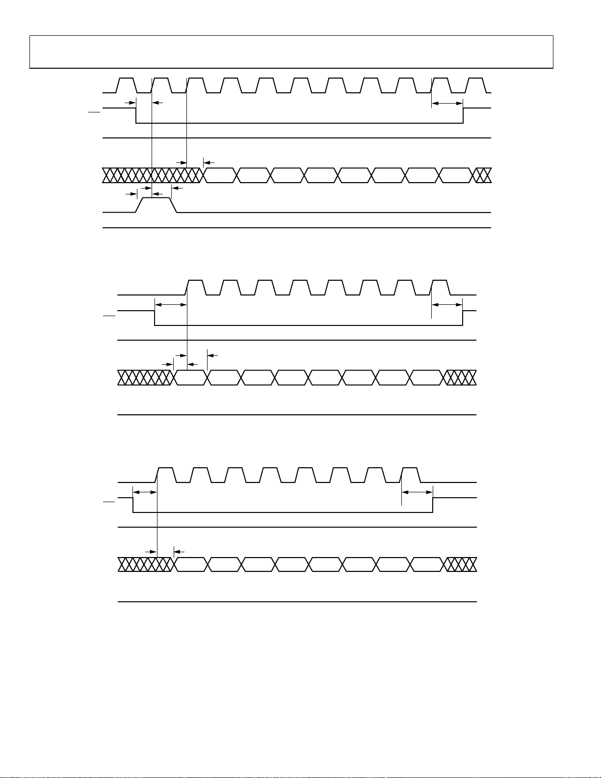
Figure 15. MNM Microport Write Timing Requirements
Rev. 0 | Page 16 of 72
AD6636
t
K
CPUCL
DD
DDTACK
t
t
t
HC
t
HC
HC
HAM
04998-0-016
t
SC
DS
t
SC
R/W
t
SC
CS
t
SAM
A [7:0]
VALID ADDRESS
t
D [15:0]
VALID
DATA
t
DTACK
NOTE:
ACCESS TIME DEPENDS ON THE ADDRESS ACCESSED. IT CAN VARY FROM 3 TO 9 CPUCLK CYCLES.
ACC
t
ACC
Figure 16 MNM Microport Read Timing Requirements
SCLK
t
SCS
SMODE
SDI
SRFS
MODE
t
SSRFS
SSCS
t
HSI
t
SSI
D0 D1 D2 D3 D4 D5 D6 D7
t
HSRFS
LOGIC 1
LOGIC 1
t
HSCS
04998-0-017
Figure 17. SPORT Mode Write Timing Characteristics
Rev. 0 | Page 17 of 72
AD6636
SCLK
SCS
t
SSCS
t
HSCS
SMODE
SDO
STFS
MODE
t
SSTFS
t
HSTFS
t
DSDO
D0 D1 D2 D3 D4 D5 D6 D7
LOGIC 1
LOGIC 1
04998-0-018
Figure 18. SPORT Mode Read Timing Characteristics
SCLK
SCS
SMODE
SDI
MODE
t
SSCS
t
HSI
t
SSI
D0 D1 D2 D3 D4 D5 D6 D7
LOGIC 1
LOGIC 0
Figure 19. SPI Mode Write Timing Characteristics
t
HSCS
04998-0-019
SCLK
SCS
SMODE
SDO
MODE
t
SSCS
LOGIC 0
t
DSDO
D0 D1 D2 D3 D4 D5 D6 D7
LOGIC 0
t
HSCS
04998-0-020
Figure 20. SPI Mode Read Timing Characteristics
Rev. 0 | Page 18 of 72

AD6636
THEORY OF OPERATION
ADC INPUT PORT
The AD6636 features four identical, independent high speed
ADC input ports named A, B, C, and D. These input ports have
the flexibility to allow independent inputs, diversity inputs, or
complex I/Q inputs. Any of the ADC input ports can be routed
to any of the six tuner channels; that is, any of the six AD6636
channels can receive input data from any of the input ports.
Time-multiplexed inputs on a single port are not supported in
the AD6636.
These four input ports can operate at up to 150 MSPS. Each
input port has its own clock (CLKA, CLKB, CLKC, and CLKD)
used for registering input data into the AD6636. To allow slow
input rates while providing fast processing clock rates, the
AD6636 contains an internal PLL clock multiplier that supplies
the internal signal processing clock. CLKA is used as an input to
the PLL clock multiplier. Additional programmability allows the
input data to be clocked into the part either on the rising edge
or the falling edge of the input clock.
The 3-exponent bits are shared with the gain range control bits
in the hardware. When floating-point ADCs are not used, these
three pins on each ADC input port can be used as gain range
control output bits.
Input Timing
The data from each high speed input port is latched either on
the rising edge or the falling edge of the port’s individual CLKx
(where x stands for A, B, C, or D input ports). The ADC clock
invert bit in ADC clock control register selects the edge of the
clock (rising or falling) used to register input data into the
AD6636.
CLKx
t
INx [15:0]
EXPx [2:0]
Figure 21. Input Data Timing Requirements
(Rising Edge of Clock, x = A, B, C, or D for Four Input Ports)
t
SI
HI
DATA n DATA n + 1
04998-0-021
In addition, the front end of the AD6636 contains circuitry that
enables high speed signal-level detection, gain control, and
quadrature I/Q correction. This is accomplished with a unique
high speed level-detection circuit that offers minimal latency
and maximum flexibility to control all four input signals
(typically ADC inputs) individually. The input ports also
provide input power-monitoring functions via various modes,
and magnitude and phase I/Q correction blocks. See the
Quadrature I/Q Correction Block section for details.
Each individual processing channel can receive input data from
any of the four input ports individually. This is controlled using
3-bit crossbar mux-select bit words in ADC input control
register. Each individual channel has a similar 3-bit selection. In
addition to the four input ports, an internal test signal (PN—
pseudorandom noise sequence) can also be selected. This
internal test signal is discussed in the User-Configurable BuiltIn Self-Test (BIST) section.
Input Data Format
Each input port consists of a 16-bit mantissa and a 3-bit
exponent (16 + 3 floating-point input, or up to 16-bit fixedpoint input). When interfacing to standard fixed-point ADCs,
the exponent bit should either be connected to ground or be
programmed as outputs for gain control output. If connected to
a floating-point ADC (also called gain ranging ADC), the
exponent bits from the ADC can be connected to the input
exponent bits of the AD6636. The mantissa data format is twos
complement, and the exponent is unsigned binary.
CLKx
t
INx [15:0]
EXPx [2:0]
Figure 22. Input Data Timing Requirements
(Falling Edge of Clock, x = A, B, C, or D for Four Input Ports)
t
SI
HI
DATA n DATA n + 1
04998-0-022
The clock signals (CLKA, CLKB, CLKC, and CLKD) can
operate at up to 150 MHz. In applications using high speed
ADCs, the ADC sample clock, data valid, or data ready strobe
are typically used to clock the AD6636.
Connection to Fixed-Point ADC
For fixed-point ADCs, the AD6636 exponent inputs, EXP[2:0],
are not typically used and should be tied low. Alternatively,
because these pins are shared with gain range control bits, if the
gain ranging block is used, these pins can be used as outputs of
the gain range control block. The ADC outputs are tied directly
to the AD6636 inputs, MSB-justified. Therefore, for fixed-point
ADCs, the exponents are typically static and no input scaling is
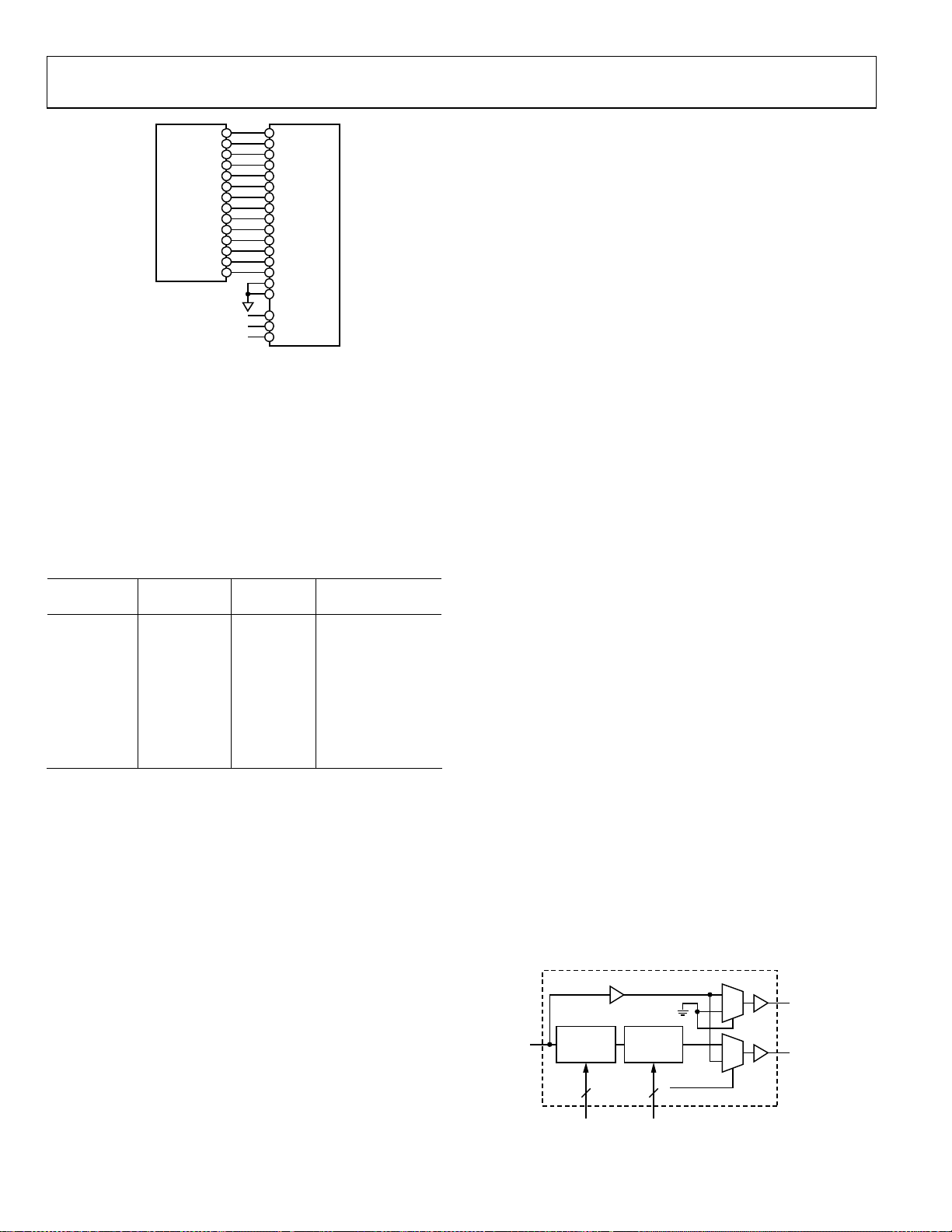
used in the AD6636. Figure 23 shows a typical interconnection.
Rev. 0 | Page 19 of 72
AD6636
A
D13 (MSB)
AD6645
14-BIT ADC
D0 (LSB)
GAIN RANGING CONTROL
BITS OR GROUNDED
EXPONENT BITS
Figure 23. Typical Interconnection of the AD6645 Fixed-Point ADC
and the AD6636
Scaling with Floating-Point ADC
An example of the exponent control feature combines the
AD6600 and the AD6636. The AD6600 is an 11-bit ADC with
three bits of gain ranging. In effect, the 11-bit ADC provides the
mantissa, and the three bits of the relative signal strength
indicator (RSSI) are the exponent. Only five of the eight
available steps are used by the AD6600. See the AD6600 data
sheet for details.
Table 9. Weighting Factors for Different Exp[2:0] Values
ADC Input
Level
AD6636
Exp[2:0]
Largest 000 (0) /1 (>> 0) 0
001 (1) /2 (>>1) 6
010 (2) /4 (>>2) 12
011 (3) /8 (>>3) 18
100 (4) /16 (>> 4) 24
101 (5) /32 (>> 5) 30
110 (6) /64 (>> 6) 36
Smallest 111 (7) /128(>> 7) 42
Complex (I/Q) Input Ports
The four individual ADC input ports of the AD6636 can be
configured to function as two complex input ports. Additionally,
if required, only two input ports can be made to function as a
complex port, while the remaining two input ports function as
real individual input ports.
In complex mode, Input Port A is paired with Input Port B to
receive I and Q data, respectively. Similarly, Input Port C can be
paired with Input Port D to receive I and Q data, respectively.
These two pairings are controlled individually using Bits 24 and
25 of ADC input control register.
As explained previously, each individual channel can receive
input signals from any of the four input ports using the crossbar
mux select bits in the ADC input control register. In addition to
the three bits, a 1-bit selection is provided for choosing the
complex input port option for any individual channel. For
example, if Channel 0 needs to receive complex input from
IN15
AD6636
IN2
IN1
IN0
EXP2
EXP1
EXP0
Data
Divide-By
04998-0-023
Signal
Attenuation (dB)
Input Ports A and B, then the mux select bits should indicate
Input Port A, and the complex input bit should be selected.
When the input ports are paired for complex input operation,
only one set of exponent bits is driven externally with gain
control output. So when Input Ports A and B form a complex
input, then EXPA[2:0] are output and, similarly, for Input Ports
C and D, EXPC[2:0] are output.
LVD S Inp ut P orts
AD6636 input ports can be configured in two different modes:
CMOS or LVDS. In CMOS input mode, the four input ports can
be configured as two complex input ports. In LVDS mode, two
CMOS input ports each are combined to form one LVDS input
port.
CMOS Input Ports INA[15:0] and INB[15:0] form the positive
and negative differential nodes, LVDS_A+[15:0] and
LVDS_A−[15:0], respectively. Similarly, INC[15:0] and
IND[15:0] form the positive and negative differential nodes,
LVDS_C+[15:0] and LVDS_C− [15:0], respectively. CLKA and
CLKB form the differential pair, LVDS_CLKA+ and
LVDS_CLKA− pins. Similarly, CLKC and CLKD form the
differential pair LVDS_CLKC+ and LVDS_CLKC− pins.
By default, the AD6636 powers up in CMOS mode and can be
programmed to CMOS mode by using the CMOS mode bit (Bit
10 of the LVDS control register). Writing Logic 1 to Bit 8 of the
LVDS control register enables an autocalibrate routine that
calibrates the impedance of the LVDS pads to match the output
impedance of the LVDS signal source impedance. The LVDS
pads in the AD6636 have an internal impedance of 100 Ω across
the differential signals; therefore, an external resistor is not
required.
PLL CLOCK MULTIPLIER
In the AD6636, the input clock rate must be the same as the
input data rate. In a typical digital down-converter architecture,
the clock rate is a limitation on the number of filter taps that
can be calculated in the programmable RAM coefficient filters
(MRCF, DRCF, and CRCF). For slower ADC clock rates (or for
any clock rate), this limitation can be overcome by using a PLL
clock multiplier to provide a higher clock rate to the RCF filters.
Using this clock multiplier, the internal signal processing clock
rate can be increased up to 200 MHz. The CLKA signal is used
as an input to the PLL clock multiplier.
PLL CLOCK GENERATION
CLK
DIVIDE BY N
(1, 2, 4 OR 8)
PLL CLOCK
MULITPLIER
(4x TO 20x)
2 5
NM
Figure 24. PLL Clock Generation
1
0
0
1
BYPASS_PLL
1 FOR BYPASS
ADC_CLK
PLL_CLK
04998-0-024
Rev. 0 | Page 20 of 72

AD6636
N
The PLL clock multiplier is programmable and uses input clock
rates between 4 MHz and 150 MHz to give a system clock rate
(output) of as high as 200 MHz.
The output clock rate is given by
MCLKA
CLKPLL
=_
where:
CLKA is the Input Port A clock rate.
M is a 5-bit programmable multiplication factor.
×
Function
The gain-control block features a programmable upper
threshold register and a lower threshold register. The ADC
input data is compared to both these registers. If ADC input
data is larger than the upper threshold register, then the gain
control output is decremented by 1. If ADC input data is smaller
than the lower threshold register, then the gain control output is
incremented by 1. When decrementing the gain control output,
the change is immediate. But when incrementing the output, a
dwell-time register is used to delay the change. If the ADC input
is larger than the upper threshold register value, the gaincontrol output is decremented immediately to prevent overflow.
N is a predivide factor.
M is a 5-bit number between 4 and 20 (both values included). N
(predivide) can be 1, 2, 4, or 8. The multiplication factor
programmed using a 5-bit PLL clock multiplier word in the
ADC clock control register. A value outside the valid range of 4
to 20 bypasses the PLL clock multiplier and, therefore, the PLL
clock is the same as the input clock. The predivide factor
programmed using a 2-bit ADC pre-PLL clock divider word in
the ADC clock control register, as listed in Table 10.
Table 10. PLL Clock Generation Predivider Control
Predivide Word [1:0] Divide-by Value for the Clock
00 Divide-by-1, bypass
01 Divide-by-2
10 Divide-by-4
11 Divide-by-8
For best signal processing advantage, the user should program
the clock multiplier to give a system clock output as close as
possible to, but not exceeding, 200 MHz. The internal blocks of
the AD6636 that run off of the PLL clock are rated to run at a
maximum of 200 MHz. The default power-up state for the PLL
clock multiplier is the bypass state, where CLKA is passed on as
the PLL clock.
M is
N is
ADC GAIN CONTROL
Each ADC input port has individual, high speed gain-control
logic circuitry. Such gain-control circuitry is useful in applications that involve large dynamic-range inputs or in which
gain-ranging ADCs are employed. The AD6636 gain-control
logic allows programmable upper and lower thresholds and a
programmable dwell-time counter for temporal hysteresis.
When the ADC input is lower than the lower threshold register,
a dwell timer is loaded with the value in the programmable
20-bit dwell-time register. The counter decrements once every
input clock cycle, as long as the input signal remains below the
lower threshold register value. If the counter reaches 1, the gain
control output is incremented by 1. If the signal goes above the
lower threshold register value, the gain adjustment is not made,
and the normal comparison to lower and upper threshold
registers is initiated once again. Therefore, the dwell timer
provides temporal hysteresis and prevents the gain from
switching continuously.
In a typical application, if the ADC signal goes below the lower
threshold for a time greater than the dwell time, then the gain
control output is incremented by 1. Gain control bits control the
gain ranging block, which appears before the ADC in the signal
chain. With each increment of the gain control output, gain in
the gain-ranging block is increased by 6.02 dB. This increases
the dynamic range of the input signal into the ADC by 6.02 dB.
This gain is compensated for in the AD6636 by relinearizing, as
explained in the Relinearization section. Therefore, the AD6636
can increase the dynamic range of the ADC by 42 dB, provided
that the gain-ranging block can support it.
Relinearization
The gain in the gain-ranging block (external) is compensated
for by relinearizing, using the exponent bits EXP[2:0] of the
input port. For this purpose, the gain control bits are connected
to the EXP[2:0] bits, providing an attenuation of 6.02 dB for
every increase in the gain control output. After the gain in the
external gain-ranging block and the attenuation in the AD6636
(using EXP bits), the signal gain is essentially unchanged. The
only change is the increase in the dynamic range of the ADC.
Each input port has a 3-bit output from the gain control block.
These three output pins are shared with the 3-bit exponent
input pins for each input port. The operation is controlled by
the gain control enable bit in gain control register of the
individual input ports. A Logic 1 in this bit programs the
EXP[2:0] pins as gain-control outputs, and a Logic 0 configures
the pins as input exponent pins. To avoid bus contention, these
pins are set, by default, as input exponent pins.
Rev. 0 | Page 21 of 72
External gain-ranging blocks or gain-ranging ADCs have a
delay associated with changing the gain of the signal. Typically,
these delays can be up to 14 clock cycles. The gain change in the
AD6636 (via EXP[2:0]) must be synchronized with the gain
change in the gain-ranging block (external). This is allowed in
the AD6636 by providing a flexible delay, programmable 6-bit
word in the gain control register. The value in this 6-bit word
gives the delay in input clock cycles. A programmable pipeline
AD6636
delay given by the 6-bit value (maximum delay of 63 clock
cycles) is placed between the gain control output and the
EXP[2:0] input. Therefore, the external gain-ranging block’s
settling delays are compensated for in the AD6636.
Note that any gain changes that are initiated during the
relinearization period are ignored. For example, if the AD6636
detects that a gain adjustment is required during the relinearization period of a previous gain adjustment, then the new
adjustment is ignored.
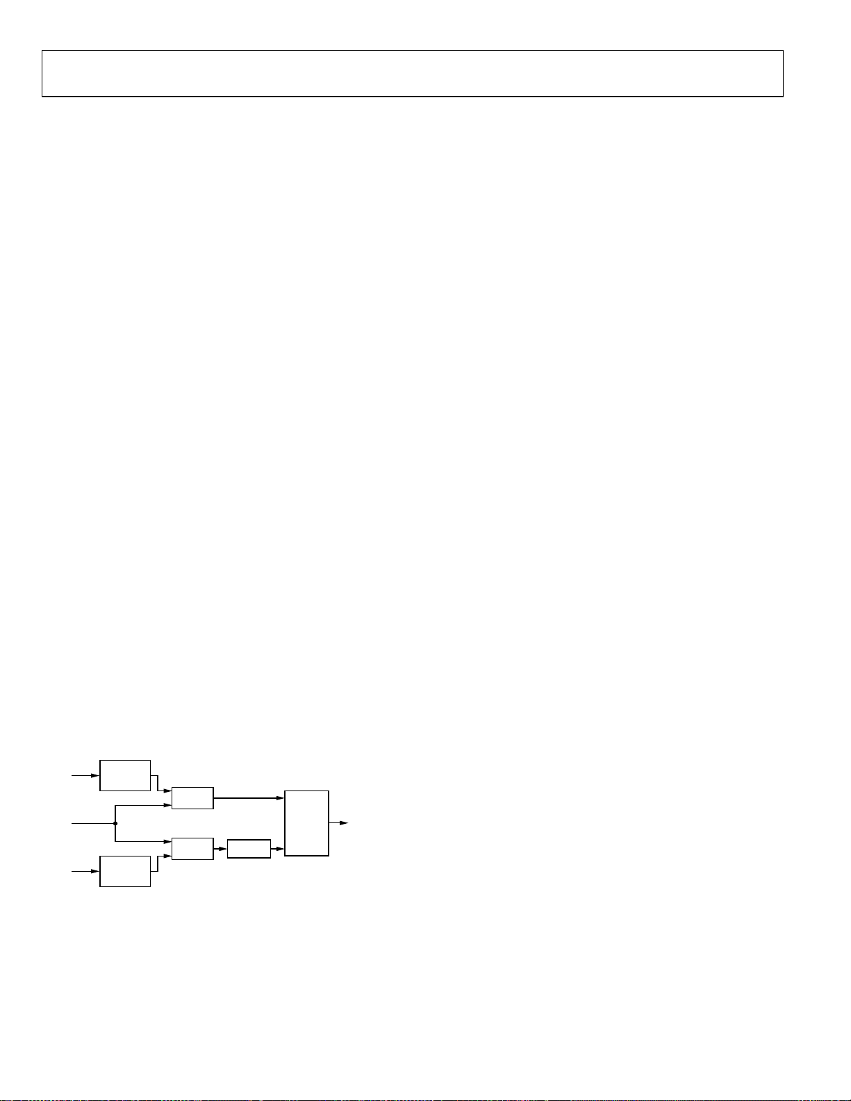
Setting Up the Gain Control Block
To set up the gain control block for individual input ports, the
individual upper threshold registers and lower threshold
registers should be written with appropriate values. The 10-bit
values written into upper and lower threshold registers are
compared to the 10 MSB bits of the absolute magnitude
calculated using the input port data. The 20-bit dwell timer
register should have the appropriate number of clock cycles to
provide temporal hysteresis.
ADC INPUT PORT MONITOR FUNCTION
The AD6636 provides a power-monitor function that can
monitor and gather statistics about the received signal in a
signal chain. Each input port is equipped with an individual
power-monitor function that can operate both in real and in
complex modes of the input port. This function block can
operate in one of three modes, which measure the following
over a programmable period of time:
•
Peak power
Mean power
•
Number of samples crossing a threshold
•
These functions are controlled via the 2-bit power-monitor
function select bits of the power monitor control register for
each individual input port. The input ports can be set for
different modes, but only one function can be active at a time
for any given input port.
A 6-bit relinearization pipeline delay word is set to synchronize
with the settling delay in the external gain ranging circuitry.
Finally, the gain control enable bit is written with Logic 1 to
activate the gain control block. On enabling, the gain control
output bits are made 000 (output on EXP[2:0] pins), which
represent the minimum gain for the external gain-ranging
circuitry and corresponding minimum attenuation during
relinearization. The normal functioning takes over, as explained
previously in this section.
Complex Inputs
For complex inputs (formed by pairing two input ports), only
one set of EXP[2:0] pins should be used as the gain control
output. For the pair of Input Ports A and B, gain control
circuitry for Input Port A is active, and EXPA[2:0] should be
connected externally as the gain control output. The gain
control circuitry for Input Port B is not activated (shut down),
and EXPB[2:0] is forced to be equal to EXP[2:0].
FROM
MEMORY
FROM INPUT
MEMORY
MAP
PORTS
FROM
MAP
LOWER
THRESHOLD
REGISTER
LOWER
THRESHOLD
REGISTER
Figure 25. AD6636 Gain Control Block Diagram
B
A
B
A
COMPARE
A > B
COMPARE
A < B
DECREASE
EXTERNAL GAIN
INCREASE
EXTERNAL GAIN
DWELL
TIMER
INC
EXP GEN
DEC
EXP [2:0]
04998-0-025
The three modes of operation can function continuously over a
programmable time period. This time period is programmed as
the number of input clock cycles in a 24-bit ADC monitor
period register (AMPR). This register is separate for each input
port. An internal magnitude storage register (MSR) is used to
monitor, accumulate, or count, depending on the mode of
operation.
Peak Detector Mode (Control Bits 00)
The magnitude of the input port signal is monitored over a
programmable time period (given by AMPR) to give the peak
value detected. This mode is set by programming Logic 0 in the
power-monitor function select bits of the power-monitor
control register for each individual input port. The 24-bit
AMPR must be programmed before activating this mode.
After enabling this mode, the value in the AMPR is loaded into
a monitor period timer and the countdown is started. The
magnitude of the input signal is compared to the MSR, and the
greater of the two is updated back into the MSR. The initial
value of the MSR is set to the current ADC input signal
magnitude. This comparison continues until the monitor period
timer reaches a count of 1.
When the monitor period timer reaches a count of 1, the value
in the MSR is transferred to the power-monitor holding register,
which can be read through the microport or the serial port. The
monitor period timer is reloaded with the value in the AMPR,
and the countdown is started. Also, the first input sample’s
magnitude is updated in the MSR, and the comparison and
update procedure, as explained above, continues. If the interrupt
is enabled, an interrupt is generated, and the interrupt status
register is updated when the AMPR reaches a count of 1.
Rev. 0 | Page 22 of 72
 Loading...