Quad, 16-/12-Bit nanoDAC+
V
V
Data Sheet
FEATURES
High relative accuracy (INL): ±2 LSB maximum @ 16 bits
Tiny package: 3 mm × 3 mm, 16-lead LFCSP
Total unadjusted error (TUE): ±0.1% of FSR maximum
Offset error: ±1.5 mV maximum
Gain error: ±0.1% of FSR maximum
High drive capability: 20 mA, 0.5 V from supply rails
User selectable gain of 1 or 2 (GAIN pin)
Reset to zero scale or midscale (RSTSEL pin)
1.8 V logic compatibility
50 MHz SPI with readback or daisy chain
Low glitch: 0.5 nV-sec
Robust 4 kV HBM and 1.5 kV FICDM ESD rating
Low power: 1.8 mW at 3 V
2.7 V to 5.5 V power supply
−40°C to +105°C temperature range
APPLICATIONS
Digital gain and offset adjustment
Programmable attenuators
Process control (PLC I/O cards)
Industrial automation
Data acquisition systems
V
LOGIC
SCLK
SYNC
SDIN
SDO
with SPI Interface
AD5686/AD5684
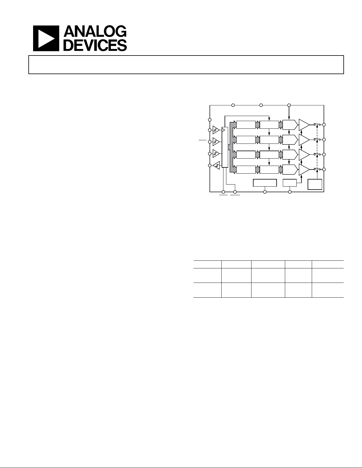
FUNCTIONAL BLOCK DIAGRAM
DD
AD5686/AD5684
INPUT
REGISTER
INPUT
REGISTER
INPUT
REGISTER
INTERF AC E LOGIC
INPUT
REGISTER
GND
DAC
REGISTER
DAC
REGISTER
DAC
REGISTER
DAC
REGISTER
POWER-ON
RESET
RSTSEL GAINLDAC RESET
Figure 1.
REF
STRING
DAC A
STRING
DAC B
STRING
DAC C
STRING
DAC D
GAIN
×1/×2
BUFFER
BUFFER
BUFFER
BUFFER
POWER-
DOWN
LOGIC
V
A
OUT
V
B
OUT
V
C
OUT
V
D
OUT
10797-001
GENERAL DESCRIPTION
The AD5686/AD5684, members of the nanoDAC+™ family, are
low power, quad, 16-/12-bit buffered voltage output DACs.
The devices include a gain select pin giving a full-scale output
of 2.5 V (gain = 1) or 5 V (gain = 2). All devices operate from
a single 2.7 V to 5.5 V supply, are guaranteed monotonic by
design, and exhibit less than 0.1% FSR gain error and 1.5 mV
offset error performance. The devices are available in a 3 mm
× 3 mm LFCSP and a TSSOP package.
The AD5686/AD5684 also incorporate a power-on reset circuit
and a RSTSEL pin that ensures that the DAC outputs power up
to zero scale or midscale and remain at that level until a valid
write takes place. Each part contains a per-channel power-down
feature that reduces the current consumption of the device to
4 μA at 3 V while in power-down mode.
The AD5686/AD5684 employ a versatile SPI interface that
operates at clock rates up to 50 MHz, and all devices contain
a V
pin intended for 1.8 V/3 V/5 V logic.
LOGIC
Rev. 0
Information furnished by Analog Devices is believed to be accurate and reliable. However, no
responsibility is assumed by Analog Devices for its use, nor for any infringements of patents or other
rights of third parties that may result from its use. Specifications subject to change without notice. No
license is granted by implication or otherwise under any patent or patent rights of Analog Devices.
Trademarks and registered trademarks are the property of their respective owners.
Table 1. Quad nanoDAC+ Devices
Interface Reference 16-Bit 14-Bit 12-Bit
SPI Internal AD5686R AD5685R AD5684R
SPI External AD5686 AD5684
I2C Internal AD5696R AD5695R AD5694R
I2C External AD5696 AD5694
PRODUCT HIGHLIGHTS
1. High Relative Accuracy (INL).
AD5686 (16-bit): ±2 LSB maximum
AD5684 (12-bit): ±1 LSB maximum
2. Excellent DC Performance.
Tota l u n adj u ste d e r ror : ±0 . 1% o f FS R ma x imu m
Offset error: ±1.5 mV maximum
Gain error: ±0.1% of FSR maximum
3. Two Pa ckage Options.
3 mm × 3 mm, 16-lead LFCSP
16-lead TSSOP
One Technology Way, P.O. Box 9106, Norwood, MA 02062-9106, U.S.A.
Tel: 781.329.4700 www.analog.com
Fax: 781.461.3113 ©2012 Analog Devices, Inc. All rights reserved.

AD5686/AD5684 Data Sheet
TABLE OF CONTENTS
Features .............................................................................................. 1
Applications ....................................................................................... 1
Functional Block Diagram .............................................................. 1
General Description ......................................................................... 1
Product Highlights ........................................................................... 1
Revision History ............................................................................... 2
Specifications ..................................................................................... 3
AC Characteristics ........................................................................ 5
Timing Characteristics ................................................................ 6
Daisy-Chain and Readback Timing Characteristics................ 7
Absolute Maximum Ratings ............................................................ 9
ESD Caution .................................................................................. 9
Pin Configurations and Function Descriptions ......................... 10
Typical Performance Characteristics ........................................... 11
Terminology .................................................................................... 16
Theory of Operation ...................................................................... 18
Digital-to-Analog Converter .................................................... 18
Transfer Function ....................................................................... 18
DAC Architecture ....................................................................... 18
Serial Interface ............................................................................ 19
Standalone Operation ................................................................ 20
Write and Update Commands .................................................. 20
Daisy-Chain Operation ............................................................. 20
Readback Operation .................................................................. 21
Power-Down Operation ............................................................ 21
Load DAC (Hardware
LDAC
Mask Register ................................................................. 22
Hardware Reset (
Reset Select Pin (RSTSEL) ........................................................ 23
Applications Information .............................................................. 24
Microprocessor Interfacing ....................................................... 24
AD5686/AD5684 to ADSP-BF531 Interface .......................... 24
AD5686/AD5684 to SPORT Interface .................................... 24
Layout Guidelines....................................................................... 24
Galvanically Isolated Interface ................................................. 25
Outline Dimensions ....................................................................... 26
Ordering Guide .......................................................................... 27
LDAC
Pin) ........................................... 22
) .......................................................... 23
RESET
REVISION HISTORY
7/12—Revision 0: Initial Version
Rev. 0 | Page 2 of 28

Data Sheet AD5686/AD5684
1
STATIC PERFORMANCE2
AD5686
Resolution
16
16
Bits
Gain Temperature
REF
REF
REF
REF
OUT
OUT
DD
REF
LOGIC
REF
LOGIC
SPECIFICATIONS
VDD = 2.7 V to 5.5 V; V
= 2.5 V; 1.8 V ≤ V
REF
≤ 5.5 V; all specifications T
LOGIC
MIN
to T
, unless otherwise noted. RL = 2 kΩ; CL = 200 pF.
MAX
Table 2.
A Grade1
B Grade
Parameter Min Typ Max Min Typ Max Unit Test Conditions/Comments
Relative Accuracy ±2 ±8 ±1 ±2 LSB Gain = 2
±2 ±8 ±1 ±3 LSB Gain = 1
Differential Nonlinearity ±1 ±1 LSB Guaranteed monotonic by design
AD5684
Resolution 12 12 Bits
Relative Accuracy ±0.12 ±2 ±0.12 ±1 LSB
Differential Nonlinearity ±1 ±1 LSB Guaranteed monotonic by design
Zero-Code Error 0.4 4 0.4 1.5 mV All 0s loaded to DAC register
Offset Error +0.1 ±4 +0.1 ±1.5 mV
Full-Scale Error +0.01 ±0.2 +0.01 ±0.1
Gain Error ±0.02 ±0.2 ±0.02 ±0.1
Total Unadjusted Error ±0.01 ±0.25 ±0.01 ±0.1
±0.25 ±0.2
Offset Error Drift
±1 ±1 µV/°C
3
±1 ±1 ppm Of FSR/°C
Coefficient3
DC Power Supply Rejection
3
Ratio
DC Crosstalk3
0.15 0.15 mV/V DAC code = midscale; V
±2 ±2 µV
±3 ±3 µV/mA Due to load current change
±2 ±2 µV Due to powering down (per channel)
OUTPUT CHARACTERISTICS3
Output Voltage Range 0 V
0 2 × V
0 V
0 2 × V
Capacitive Load Stability 2 2 nF RL = ∞
10 10 nF RL = 1 kΩ
Resistive Load4 1 1 kΩ
Load Regulation 80 80 µV/mA
80 80 µV/mA
Short-Circuit Current5 40 40 mA
Load Impedance at Rails6 25 25 Ω See Figure 23
Power-Up Time 2.5 2.5 µs
REFERENCE INPUT
Reference Current 90 90 µA V
180 180 µA V
Reference Input Range 1 VDD 1 VDD V Gain = 1
1 VDD/2 1 VDD/2 V Gain = 2
Reference Input Impedance 16 16 kΩ Gain = 2
32 32 kΩ Gain = 1
% of
FSR
% of
FSR
% of
FSR
% of
FSR
V Gain = 1
V Gain = 2, see Figure 23
All 1s loaded to DAC register
Gain = 2
Gain = 1
= 5 V ± 10%
DD
Due to single channel, full-scale
output change
5 V ± 10%, DAC code = midscale;
−30 mA ≤ I
≤ +30 mA
3 V ± 10%, DAC code = midscale;
−20 mA ≤ I
≤ +20 mA
Coming out of power-down mode;
V
= 5 V
= VDD = V
= VDD = V
=5.5 V, gain = 1
=5.5 V, gain = 2
Rev. 0 | Page 3 of 28

AD5686/AD5684 Data Sheet
1
INL
LOGIC
LOGIC
INH
LOGIC
LOGIC
SINK
LOGIC
LOGIC
SOUR CE
POWER REQUIREMENTS
REF
REF
A Grade1
B Grade
Parameter Min Typ Max Min Typ Max Unit Test Conditions/Comments
LOGIC INPUTS3
Input Current ±2 ±2 µA Per pin
Input Low Voltage (V
Input High Voltage (V
) 0.3 × V
) 0.7 × V
0.7 × V
0.3 × V
V
V
Pin Capacitance 2 2 pF
LOGIC OUTPUTS (SDO)3
Output Low Voltage, VOL 0.4 0.4 V I
Output High Voltage, VOH V
Floating State Output
− 0.4 V
− 0.4 V I
4 4 pF
= 200 μA
= 200 μA
Capacitance
V
I
LOGIC
LOGIC
1.8 5.5 1.8 5.5 V
3 3 µA
VDD 2.7 5.5 2.7 5.5 V Gain = 1
V
+ 1.5 5.5 V
+ 1.5 5.5 V Gain = 2
IDD VIH = VDD, VIL = GND, VDD = 2.7 V to 5.5 V
Normal Mode7 0.59 0.7 0.59 0.7 mA
All Power-Down Modes8 1 4 1 4 µA −40°C to +85°C
6 6 µA −40°C to +105°C
1
Temperature range, A and B grade: −40°C to +105°C.
2
DC specifications tested with the outputs unloaded, unless otherwise noted. Upper dead band = 10 mV and exists only when V
with gain = 2. Linearity calculated using a reduced code range of 256 to 65,280 (AD5686) or 12 to 4080 (AD5684).
V
DD
3
Guaranteed by design and characterization; not production tested.
4
Channel A and Channel B can have a combined output current of up to 30 mA. Similarly, Channel C and Channel D can have a combined output current of up to
30 mA up to a junction temperature of 110°C.
5
VDD = 5 V. The device includes current limiting that is intended to protect the device during temporary overload conditions. Junction temperature can be exceeded
during current limit. Operation above the specified maximum operation junction temperature may impair device reliability.
6
When drawing a load current at either rail, the output voltage headroom with respect to that rail is limited by the 25 Ω typical channel resistance of the output
devices. For example, when sinking 1 mA, the minimum output voltage = 25 Ω × 1 mA = 25 mV (see Figure 23).
7
Interface inactive. All DACs active. DAC outputs unloaded.
8
All DACs powered down.
= VDD with gain = 1 or when V
REF
REF
/2 =
Rev. 0 | Page 4 of 28

Data Sheet AD5686/AD5684
Total Harmonic Distortion4
−80 dB
At ambient, BW = 20 kHz, VDD = 5 V, f
OUT
= 1 kHz
OUT
OUT
OUT
AC CHARACTERISTICS
VDD = 2.7 V to 5.5 V; V
otherwise noted.
1
Table 3.
Parameter2 Min Typ Max Unit Test Conditions/Comments3
Output Voltage Settling Time
AD5686 5 8 µs ¼ to ¾ scale settling to ±2 LSB
AD5684 5 7 µs ¼ to ¾ scale settling to ±2 LSB
Slew Rate 0.8 V/µs
Digital-to-Analog Glitch Impulse 0.5 nV-sec 1 LSB change around major carry
Digital Feedthrough 0.13 nV-sec
Multiplying Bandwidth 500 kHz
Digital Crosstalk 0.1 nV-sec
Analog Crosstalk 0.2 nV-sec
DAC-to-DAC Crosstalk 0.3 nV-sec
Output Noise Spectral Density 100 nV/√Hz DAC code = midscale, 10 kHz; gain = 2
Output Noise 6 µV p-p 0.1 Hz to 10 Hz
SNR 90 dB At ambient, BW = 20 kHz, VDD = 5 V, f
SFDR 83 dB At ambient, BW = 20 kHz, VDD = 5 V, f
SINAD 80 dB At ambient, BW = 20 kHz, VDD = 5 V, f
1
Guaranteed by design and characterization; not production tested.
2
See the Terminology section.
3
Temperature range is −40°C to +105°C, typical @ 25°C.
4
Digitally generated sine wave @ 1 kHz.
= 2.5 V; 1.8 V ≤ V
REF
≤ 5.5 V; RL = 2 kΩ to GND; CL = 200 pF to GND; all specifications T
LOGIC
to T
MIN
= 1 kHz
= 1 kHz
= 1 kHz
MAX
, unless
Rev. 0 | Page 5 of 28
AD5686/AD5684 Data Sheet
LOGIC
LOGIC
Data Setup Time
t5 8 5
ns
t
4
t
3
SCLK
SYNC
SDIN
t
1
t
2
t
5
t
6
t
7
t
8
DB23
t
9
t
10
t
11
LDAC
1
LDAC
2
t
12
1
ASYNCHRONOUS LDAC UPDATE MODE .
2
SYNCHRONOUS LDAC UPDATE MODE .
RESET
t
13
t
14
V
OUT
DB0
10797-002
TIMING CHARACTERISTICS
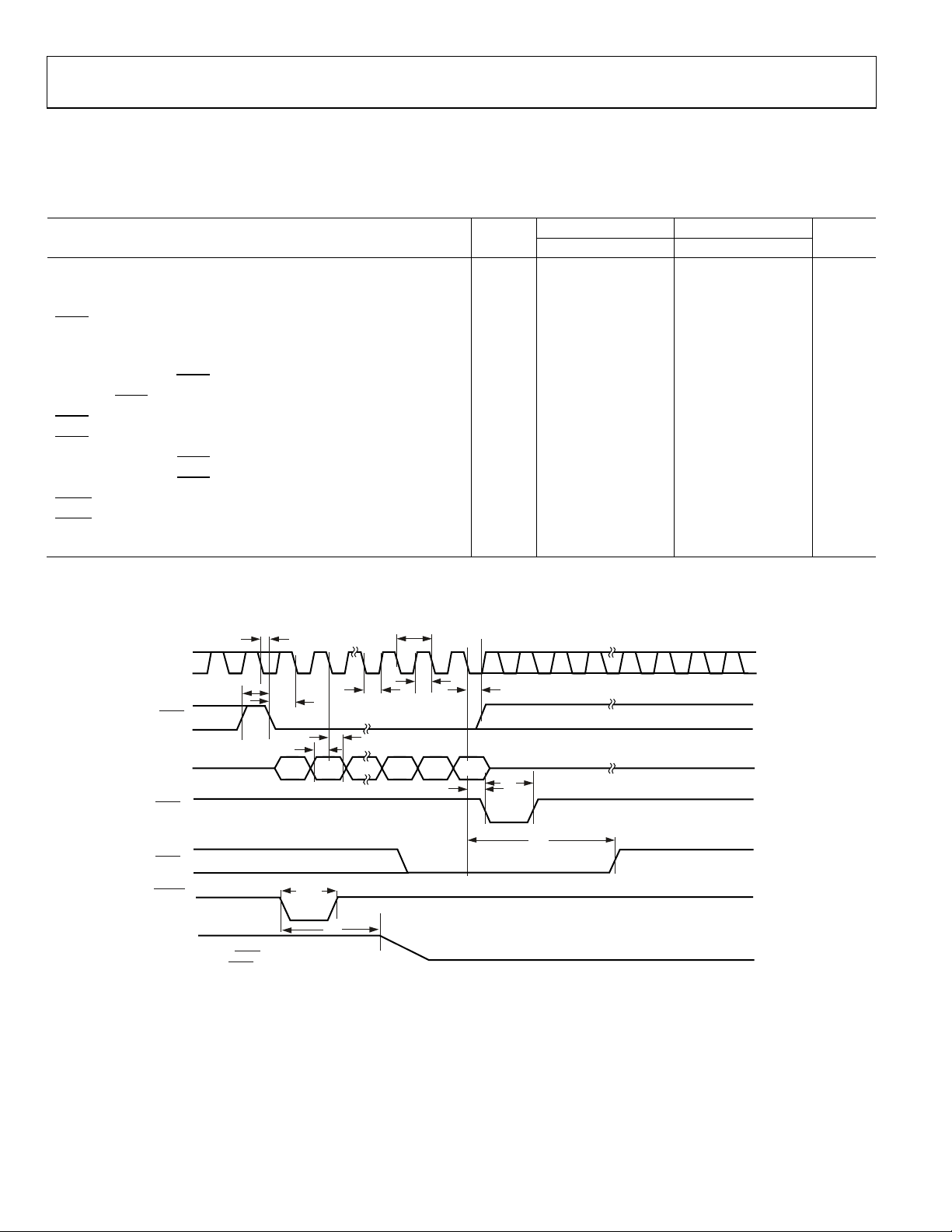
All input signals are specified with tR = tF = 1 ns/V (10% to 90% of VDD) and timed from a voltage level of (VIL + VIH)/2. See Figure 2.
V
= 2.7 V to 5.5 V, 1.8 V ≤ V
DD
Table 4.
1.8 V ≤ V
Parameter1 Symbol Min Max Min Max Unit
SCLK Cycle Time t1 33 20 ns
SCLK High Time t2 16 10 ns
SCLK Low Time t3 16 10 ns
to SCLK Falling Edge Setup Time t4 15 10 ns
SYNC
Data Hold Time t6 8 5 ns
SCLK Falling Edge to
Minimum
Falling Edge to SCLK Fall Ignore t9 16 10 ns
SYNC
Pulse Width Low t10 25 15 ns
LDAC
High Time t8 20 20 ns
SYNC
SCLK Falling Edge to
SCLK Falling Edge to
Minimum Pulse Width Low t13 30 30 ns
RESET
Pulse Activation Time t14 30 30 ns
RESET
Rising Edge t7 15 10 ns
SYNC
Rising Edge t11 30 20 ns
LDAC
Falling Edge t12 20 20 ns
LDAC
Power-Up Time2 4.5 4.5 µs
1
Maximum SCLK frequency is 50 MHz at VDD = 2.7 V to 5.5 V, 1.8 V ≤ V
2
Time to exit power-down to normal mode of AD5686/AD5684 operation, 32nd clock edge to 90% of DAC midscale value, with output unloaded.
LOGIC
≤ 5.5 V; V
= 2.5 V. All specifications T
REF
≤ VDD. Guaranteed by design and characterization; not production tested.
LOGIC
MIN
to T
, unless otherwise noted.
MAX
< 2.7 V 2.7 V ≤ V
≤ 5.5 V
Figure 2. Serial Write Operation
Rev. 0 | Page 6 of 28
Data Sheet AD5686/AD5684
LOGIC
LOGIC
200µA I
OL
200µA I
OH
V
OH
(MIN)
TO OUTPUT
PIN
C
L
20pF
10797-003
t
4
t
5
t
6
t
8
SDO
SDIN
SYNC
SCLK
4824
DB23 DB0 DB23 DB0
DB23
INPUT WORD FOR DAC NUNDEFINED
INPUT WORD FOR DAC N + 1INPUT WORD FOR DAC N
DB0
t
11
t
12
t
10
10797-004
DAISY-CHAIN AND READBACK TIMING CHARACTERISTICS
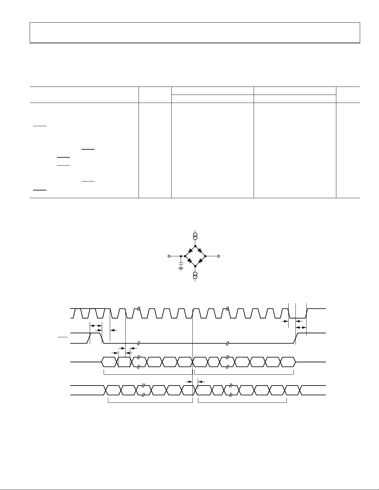
All input signals are specified with tR = tF = 1 ns/V (10% to 90% of VDD) and timed from a voltage level of (VIL + VIH)/2. See Figure 4
and Figure 5. V
Table 5.
1.8 V ≤ V
Parameter1 Symbol Min Max Min Max Unit
SCLK Cycle Time t1 66 40 ns
SCLK High Time t2 33 20 ns
SCLK Low Time t3 33 20 ns
to SCLK Falling Edge t4 33 20 ns
SYNC
Data Setup Time t5 5 5 ns
Data Hold Time t6 5 5 ns
SCLK Falling Edge to
Minimum
Minimum
SDO Data Valid from SCLK Rising Edge t10 36 25 ns
SCLK Falling Edge to
Rising Edge to SCLK Rising Edge t12 15 10 ns
SYNC
1
Maximum SCLK frequency is 25 MHz or 15 MHz at VDD = 2.7 V to 5.5 V, 1.8 V ≤ V
Circuit and Timing Diagrams
= 2.7 V to 5.5 V, 1.8 V ≤ V
DD
Rising Edge t7 15 10 ns
SYNC
High Time t8 60 30 ns
SYNC
High Time t9 60 30 ns
SYNC
Rising Edge t11 15 10 ns
SYNC
LOG IC
≤ 5.5 V; V
= 2.5 V. All specifications T
REF
< 2.7 V 2.7 V ≤ V
≤ VDD. Guaranteed by design and characterization; not production tested.
LOGIC
MIN
to T
, unless otherwise noted.
MAX
≤ 5.5 V
Figure 3. Load Circuit for Digital Output (SDO) Timing Specifications
Figure 4. Daisy-Chain Timing Diagram
Rev. 0 | Page 7 of 28
AD5686/AD5684 Data Sheet
SYNC
t
8
t
6
SCLK
24
1
24
1
t
9
t
4
t
2
t
7
t
3
t
1
DB23 DB0 DB23 DB0
SDIN
NOP CONDITIONINPUT WORD SPECIFIES
REGIST E R TO BE READ
t
5
DB23 DB0 DB23 DB0
SDO
SELECTED REGISTER DATA
CLOCKED OUT
UNDEFINED
t
10
10797-005
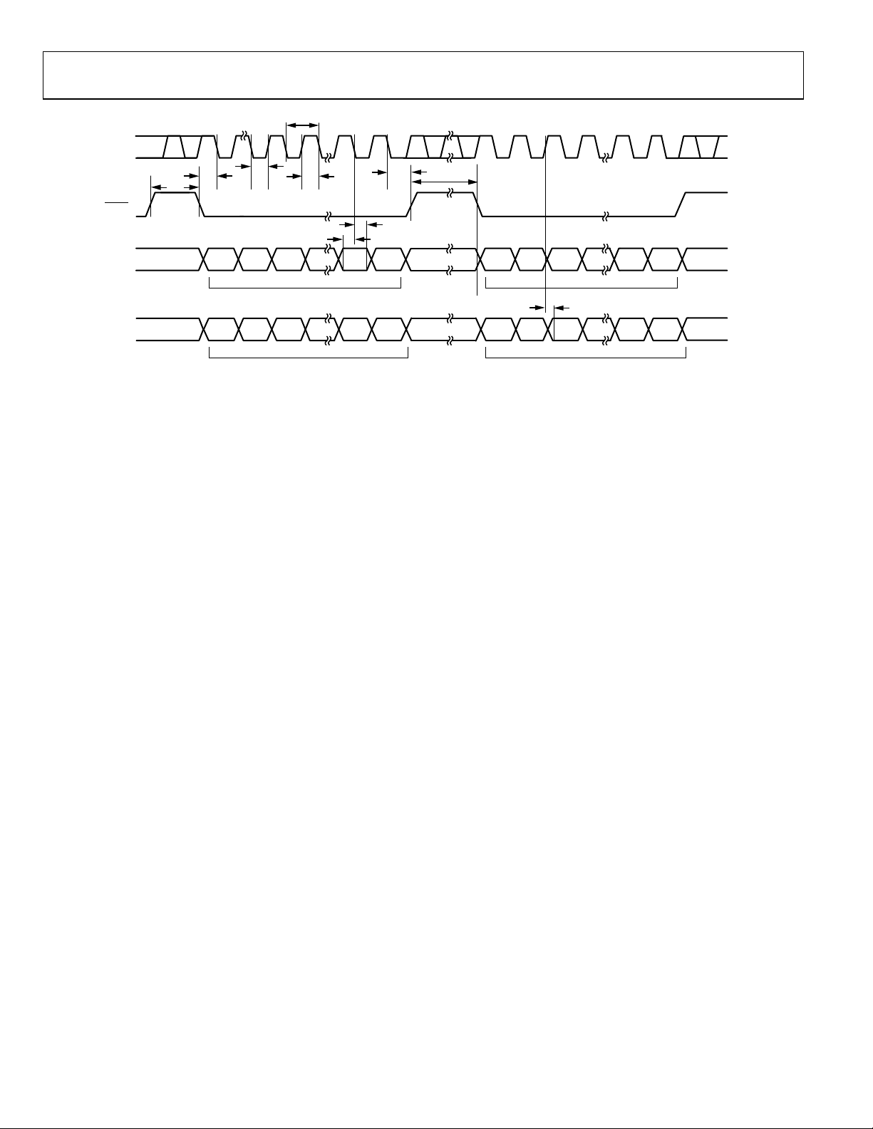
Figure 5. Readback Timing Diagram
Rev. 0 | Page 8 of 28
Data Sheet AD5686/AD5684
ABSOLUTE MAXIMUM RATINGS
TA = 25°C, unless otherwise noted.
Table 6.
Parameter Rating
VDD to GND −0.3 V to +7 V
V
to GND −0.3 V to +7 V
LOGI C
V
to GND −0.3 V to VDD + 0.3 V
OUT
V
to GND −0.3 V to VDD + 0.3 V
REF
Digital Input Voltage to GND −0.3 V to V
Operating Temperature Range −40°C to +105°C
Storage Temperature Range −65°C to +150°C
Junction Temperature 125°C
16-Lead TSSOP, θJA Thermal
Impedance, 0 Airflow (4-Layer Board)
16-Lead LFCSP, θJA Thermal
Impedance, 0 Airflow (4-Layer Board)
Reflow Soldering Peak
Temperature, Pb Free (J-STD-020)
ESD
HBM1 4 kV
FICDM 1.5 kV
1
Human body model (HBM) classification.
112.6°C/W
70°C/W
260°C
LOGI C
+ 0.3 V
Stresses above those listed under Absolute Maximum Ratings
may cause permanent damage to the device. This is a stress
rating only; functional operation of the device at these or any
other conditions above those indicated in the operational
section of this specification is not implied. Exposure to absolute
maximum rating conditions for extended periods may affect
device reliability.
ESD CAUTION
Rev. 0 | Page 9 of 28
 Loading...