ANALOG DEVICES AD5441 Service Manual

12-Bit Serial Input
FEATURES
2.5 V to 5.5 V supply operation
True 12-bit accuracy
5 V operation @ <1 μA
Fast 3-wire serial input
Fast 5 μs settling time
1.9 MHz, 4-quadrant multiply BW
Upgrade for
Standard and rotated pinout
APPLICATIONS
Ideal for PLC applications in industrial control
Programmable amplifiers and attenuators
Digitally controlled calibration and filters
Motion control systems
GENERAL DESCRIPTION
The AD5441 is an improved high accuracy 12-bit multiplying
digital-to-analog converter (DAC) in space-saving 8-lead
packages. Featuring serial input, double buffering, and excellent
analog performance, the AD5441 is ideal for applications where
PC board space is at a premium. Improved linearity and gain
error performance permit reduced part counts through the
elimination of trimming components. Separate input clock and
load DAC control lines allow full user control of data loading
and analog output.
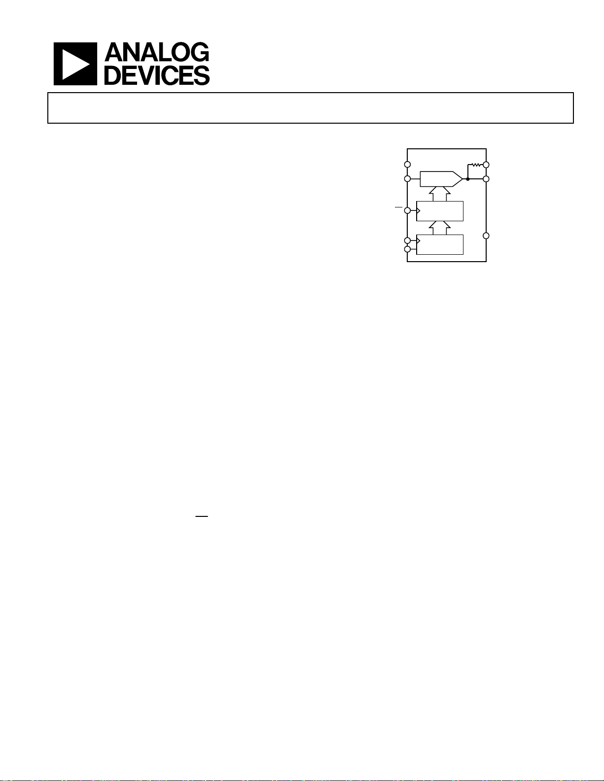
The circuit consists of a 12-bit serial-in/parallel-out shift register, a
12-bit DAC register, a 12-bit CMOS DAC, and control logic.
Serial data is clocked into the input register on the rising edge of
the clock pulse. When the new data-word is clocked in, it is
loaded into the DAC register with the
DAC register is converted to an output current by the DAC.
Consuming only 1 µA from a single 5 V power supply, the
AD5441 is the ideal low power, small size, high performance
solution to many application problems.
The AD5441 is specified over the extended industrial (−40°C to
+125°C) temperature range. It is available in an 8-lead LFCSP
and an 8-lead MSOP.
DAC8043 and DAC8043A
LD
input pin. Data in the
Multiplying DAC
AD5441
FUNCTIONAL BLOCK DIAGRAM
V
DD
V
REF
LD
CLK
SRI
AD5441
DAC
12
DAC REG
12
12-BIT SHIFT
REGISTER
Figure 1.
R
FB
I
OUT
GND
06492-001
Rev. 0
Information furnished by Analog Devices is believed to be accurate and reliable. However, no
responsibility is assumed by Anal og Devices for its use, nor for any infringements of patents or ot her
rights of third parties that may result from its use. Specifications subject to change without notice. No
license is granted by implication or otherwise under any patent or patent rights of Analog Devices.
Trademarks and registered trademarks are the property of their respective owners.
One Technology Way, P.O. Box 9106, Norwood, MA 02062-9106, U.S.A.
Tel: 781.329.4700 www.analog.com
Fax: 781.461.3113 ©2008 Analog Devices, Inc. All rights reserved.

AD5441
TABLE OF CONTENTS
Features .............................................................................................. 1
Applications....................................................................................... 1
Functional Block Diagram .............................................................. 1
General Description......................................................................... 1
Revision History ............................................................................... 2
Specifications..................................................................................... 3
Electrical Characteristics............................................................. 3
Timing Characteristics..................................................................... 4
Absolute Maximum Ratings............................................................ 5
Thermal Resistance ...................................................................... 5
ESD Caution.................................................................................. 5
Pin Configurations and Function Descriptions ...........................6
REVISION HISTORY
1/08—Revision 0: Initial Version
Typical Performance Characteristics ..............................................7
Te r mi n ol o g y .................................................................................... 10
Parameter Definitions.................................................................... 11
General Circuit Information..................................................... 11
Output Impedance ..................................................................... 11
Applications Information.......................................................... 11
Unipolar 2-Quadrant Multiplying ........................................... 11
Bipolar 4-Quadrant Multiplying.............................................. 12
Interface Logic Information...................................................... 12
Digital Section ............................................................................ 12
Outline Dimensions .......................................................................13
Ordering Guide .......................................................................... 13
Rev. 0 | Page 2 of 16

AD5441
SPECIFICATIONS
ELECTRICAL CHARACTERISTICS
VDD = 5 V, V
Table 1.
Parameter Symbol Min Typ Max Unit Condition
STATIC PERFORMANCE
Resolution N 12 Bits
Relative Accuracy INL ±0.5 LSB
Differential Nonlinearity DNL ±0.5 LSB All grades monotonic to 12 bits
Gain Error G
Gain Temperature Coefficient
Output Leakage Current I
±25 nA TA = –40°C, +125°C, data = 000H, I
Zero-Scale Error I
±0.15 LSB TA = −40°C, +125°C, data = 000H
REFERENCE INPUT
Input Resistance R
Input Capacitance
ANALOG OUTPUT
Output Capacitance
4 pF Data = FFFH
DIGITAL INPUTS
Digital Input Low VIL 0.8 V
Digital Input High VIH 2.4 V
Input Leakage Current IIL 1 μA V
Input Capacitance
AC CHARACTERISTICS
Output Current Settling Time tS 5 μs To ±0.01% of full-scale, external op amp OP42
0.5 μs To ±0.01% of full-scale, 100 Ω terminated to ground
DAC Glitch Q 40 nVs Data = 000H to FFFH to 000H, V
1 nVs Data = 000H to FFFH to 000H, V
Digital Feedthrough 5 nV Using external op amp OP42
Feedthrough (V
Total Harmonic Distortion THD −85 dB V
Output Noise Density en 17 nV/√Hz 10 Hz to 100 kHz between RFB and I
Multiplying Bandwidth BW 1.9 MHz −3 dB, V
SUPPLY CHARACTERISTICS
Power Supply Range V
Positive Supply Current IDD 10 μA V
Power Dissipation P
Power Supply Sensitivity PSS 0.002 %/% ΔVDD = ±5%
1
These parameters are guaranteed by design and not subject to production testing.
= 10 V, −40°C < TA < +155°C, unless otherwise noted.
REF
±1 LSB Data = FFFH
FSE
1
TCGFS ±5 ppm/°C I
LKG
±0.03 LSB Data = 000H
ZSE
7 15 kΩ Absolute temperature coefficient < 50 ppm/°C
1
1
1
1
) FT 1.4 mV p-p V
OUT/VREF
1
REF
C
5 pF
REF
C
OUT
CIL 4.0 pF V
DD RANGE
DISS
±5 nA Data = 000H, I
1 pF Data = 000H
2.5 5.5 V
2.5 5.5 μW V
pin measured
OUT
pin measured
OUT
= 0 V to 5 V
LOGI C
= 0 V
LOGI C
REF
REF
= 20 V p-p, data = 000H, f = 10 kHz
REF
= 6 V rms, data = FFFH, f = 1 kHz
REF
, V
= 100 mV rms, data = FFFH
REF
= 0 V or VDD
LOGI C
= 0 V or VDD
LOGI C
OUT/VREF
pin measured
OUT
= 0 V, OP42
= 0 V, 100 Ω
OUT
Rev. 0 | Page 3 of 16

AD5441
TIMING CHARACTERISTICS
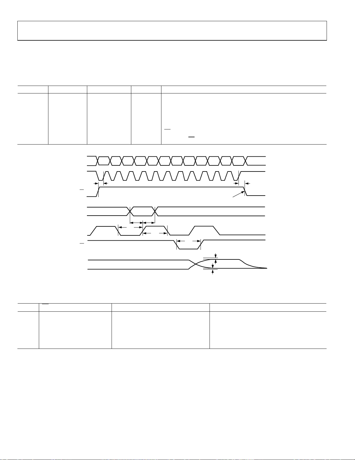
All input control signals are specified with tR = tF = 2 ns (10% to 90% of VDD) and timed from a voltage level of (VIL + VIH)/2; VDD + 2.5 V
to 5.5 V, V
Table 2. Timing Characteristics
Parameter 2.5 V 5.5 V Unit Conditions/Comments
t
DS
t
DH
t
CH
t
CL
t
LD
t
LD1
t
ASB
= 10 V; temperature range = −40°C to +125°C; all specifications T
REF
10 5 ns min Data setup
5 5 ns min Data hold
15 10 ns min Clock width high
15 10 ns min Clock width low
20 10 ns min Load pulse width
0 0 ns min
0 0 ns min
LD DAC high to MSB CLK high
LSB CLK to
to T
MIN
LD DAC
, unless otherwise noted.
MAX
SRI
CLK
LD
SRI
CLK
LD
FS
V
OUT
ZS
D11 D10D9D8 D6D5 D4D3D2D1D0D7
t
LD1
DATA LOADED MSB(D11) FIRST DAC REGISTER L OAD
t
CL
Dxx
tDSt
t
ASB
DH
t
CH
t
LD
±1LSB
ERROR BAND
6492-005
Figure 2. Timing Diagram
Table 3. Control Logic Truth Table
CLK
1
↑
↑
LD
H Shift register data advanced one bit Latched
L Shift register data advanced one bit Transparent
Serial Shift Register Function DAC Register Function
H or L L No effect Updated with current shift register contents
L
1
equals positive logic transition. ↑
1
↑
No effect Latched all 12 bits
Rev. 0 | Page 4 of 16

AD5441
ABSOLUTE MAXIMUM RATINGS
Table 4.
Parameter Rating
VDD to GND −0.3 V, +8 V
V
to GND ±18 V
REF
RFB to GND ±18 V
Logic Inputs to GND −0.3 V, VDD + 0.3 V
I
to GND −0.3 V, VDD + 0.3 V
OUT
I
Short Circuit to GND 50 mA
OUT
Package Power Dissipation (TJ max − TA)/θ
JA
Maximum Junction Temperature (TJ max) 150°C
Operating Temperature Range −40°C to +125°C
Storage Temperature Range −65°C to +150°C
Lead Temperature (Soldering, 10 sec) 300°C
Stresses above those listed under Absolute Maximum Ratings
may cause permanent damage to the device. This is a stress
rating only; functional operation of the device at these or any
other conditions above those indicated in the operational
section of this specification is not implied. Exposure to absolute
maximum rating conditions for extended periods may affect
device reliability.
THERMAL RESISTANCE
θJA is specified for the worst-case conditions, that is, a device
soldered in a circuit board for surface-mount packages.
Table 5.
Package Type θ
JA
θ
JC
Unit
8-Lead MSOP 142 44 °C/W
8-Lead LFCSP
1
Exposed pad soldered to application board.
1
75 18 °C/W
ESD CAUTION
Rev. 0 | Page 5 of 16
 Loading...