


AS7C4096-12TI
Table of contents
 Loading...
Alliance Semiconductor Corporation AS7C4096-12TI, AS7C4096-12TC, AS7C4096, AS7C4096-20TI, AS7C4096-20TC Datasheet
...
March 2001
5V/3.3V 512K × 8 CMOS SRAM
Features
• AS7C4096 (5V version)
• AS7C34096 (3.3V version)
• Industrial and commercial temperature
• Organization: 524,288 words × 8 bits
• Center power and ground pins
• High speed
- 10/12/15/20 ns address access time
- 5/6/7/8 ns output enable access time
• Low power consumption: ACTIVE
- 1375 mW (AS7C4096) / max @ 12 ns
- 468 mW (AS7C34096) / max @ 12 ns
®
• Low power consumption: STANDBY
- 110 mW (AS7C4096) / max CMOS
- 72 mW (AS7C34096) / max CMOS
• 2.0V data retention
• Equal access and cycle times
• Easy memory expansion with CE
, OE inputs
• TTL-compatible, three-state I/O
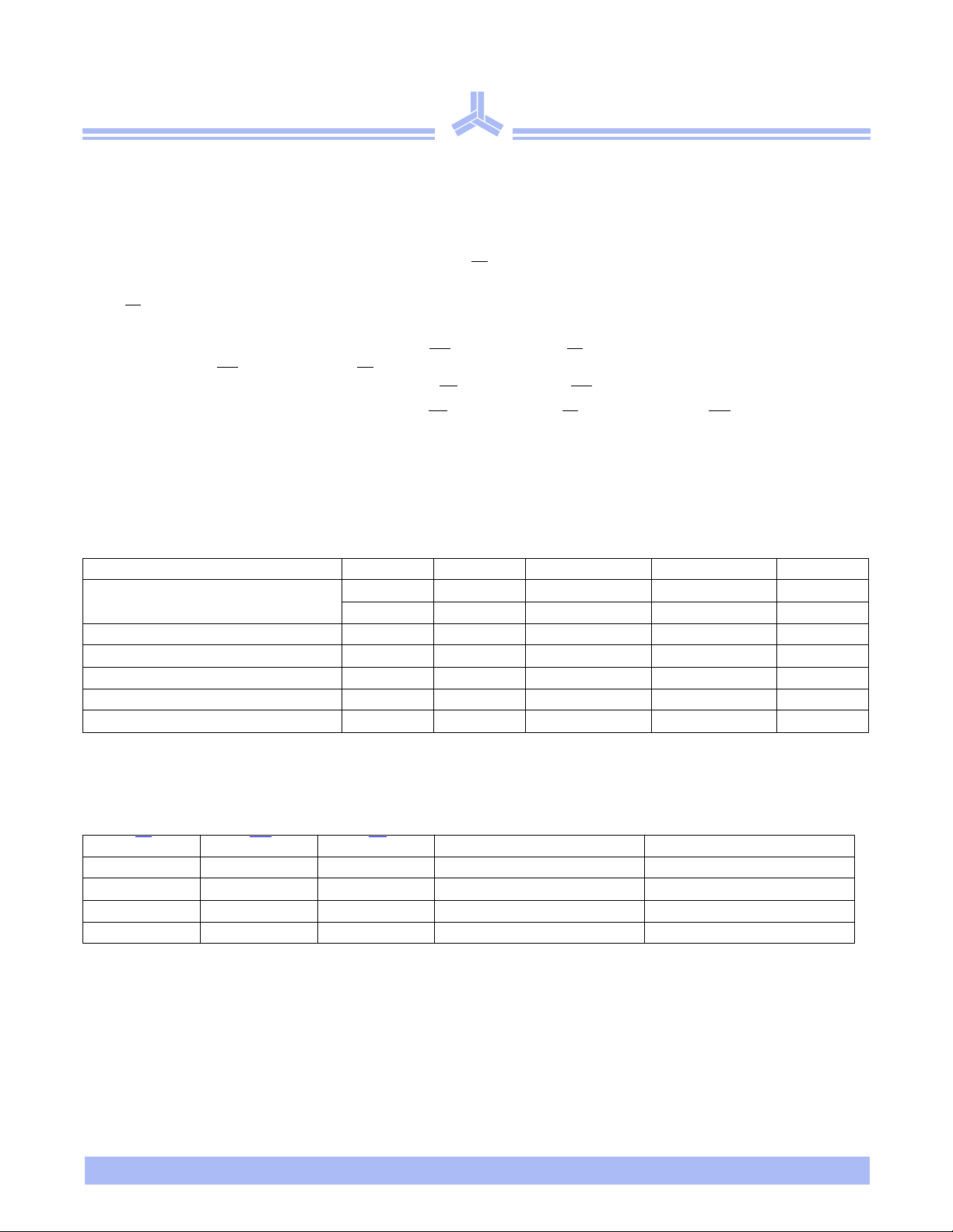
• JEDEC standard packages
- 400 mil 36-pin SOJ
- 400 mil 44-pin TSOP II
• ESD protection ≥ 2000 volts
• Latch-up current ≥ 200 mA
AS7C4096
AS7C34096
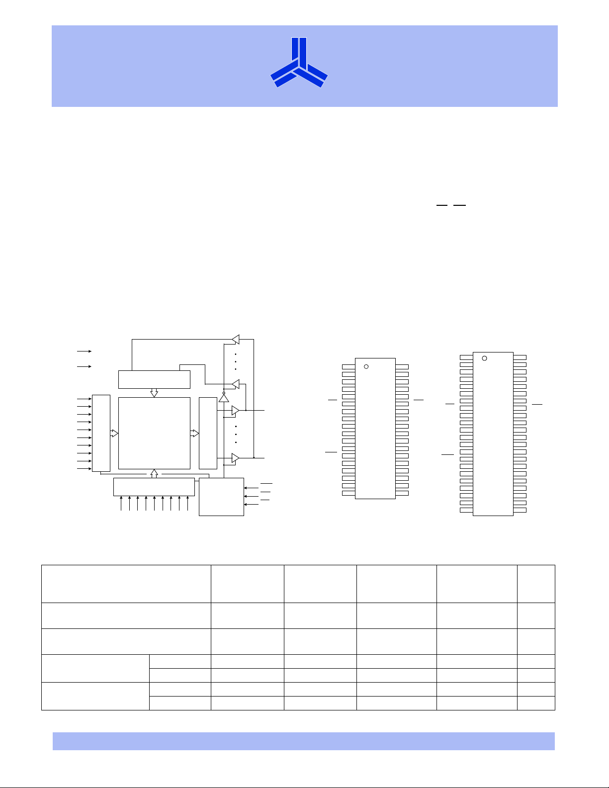
Logic block diagram
V
CC
GND
Input buffer
A0
A1
A2
A3
A4
A5
A6
A7
A8
A9
Row decoder
Column decoder
A10
524,288 × 8
(4,194,304)
A11
Selection guide
Maximum address
access time
Maximum output
enable access time
Maximum operating
current
Maximum CMOS standby
current
Pin arrangement
36-pin SOJ (400 mil) 44-pin TSOPII(400 mil)
NC
1
NC
1
36
35
34
33
32
31
30
29
28
27
26
25
24
23
22
21
20
19
–15
NC
A18
A17
A16
A15
OE
I/O8
I/O7
GND
V
CC
I/O6
I/O5
A14
A13
A12
A11
A10
NC
A0
A1
A2
A3
A4
CE
I/O1
I/O2
V
GND
I/O3
I/O4
WE
A5
A6
A7
A8
A9
Array
A12
A0
A1
A2
A3
A4
I/O1
Sense amp
Control
Circuit
A13
A14
A15
A16
A17
A18
I/O8
WE
OE
CE
CE
/O1
/O2
V
ND
/O3
/O4
WE
A5
A6
A7
A8
A9
AS7C4096
AS7C34096
–10
AS7C34096
–12
2
3
4
5
6
7
8
9
CC
10
11
12
13
14
15
16
17
18
AS7C4096
AS7C34096
10 12 15 20 ns
56 7 9ns
AS7C4096 – 250 220 180 mA
AS7C34096 160 130 110 100 mA
AS7C4096 – 20 20 20 mA
AS7C34096 20 20 20 20 mA
2
3
4
5
6
7
8
9
10
11
CC
12
13
14
15
16
17
18
19
20
NC
21
NC
22
AS7C4096
AS7C34096
–20 Unit
44
43
42
41
40
39
38
37
36
35
34
33
32
31
30
29
28
27
26
25
24
23
NC
NC
NC
A18
A17
A16
A15
OE
I/O8
I/O7
GND
V
CC
I/O6
I/O5
A14
A13
A12
A11
A10
NC
NC
NC
3/23/01; v.1.1 Alliance Semiconductor P. 1 of 10
Copyright © Alliance Semiconductor. All rights reserved.
AS7C4096
AS7C34096
®
Functional description
The AS7C4096 and AS7C34096 are high-performance CMOS 4,194,304-bit Static Random Access Memory (SRAM) devices
organized as 524,288 words × 8 bits. They are designed for memory applications where fast data access, low power, and simple
interfacing are desired.
Equal address access and cycle times (t
ideal for high-performance applications. The chip enable input CE
systems.
When CE
is high the device enters standby mode. The AS7C4096 is guaranteed not to exceed 110 mW power consumption in
CMOS standby mode. Both devices offer 2.0V data retention.
A write cycle is accomplished by asserting write enable (WE
on the rising edge of WE
(write cycle 1) or CE (write cycle 2). To avoid bus contention, external devices should drive I/O pins
only after outputs have been disabled with output enable (OE
A read cycle is accomplished by asserting output enable (OE
I/O pins with the data word referenced by the input address. When either chip enable or output enable is inactive, or write
enable is active, output drivers stay in high-impedance mode.
All chip inputs and outputs are TTL-compatible, and operation is from a single supply voltage. Both devices are available in the
industry standard 400-mil 36-pin SOJ and 44-pin TSOP II packages.
, tRC, tWC) of 10/12/15/20 ns with output enable access times (tOE) of 5/6/7/8 ns are
AA
permits easy memory expansion with multiple-bank memory
) and chip enable (CE). Data on the input pins I/O1–I/O8 is written
) or write enable (WE).
) and chip enable (CE), with write enable (WE) high. The chip drives
Absolute maximum ratings
Parameter Device Symbol Min Max Unit
Vol tag e o n V
relative to GND
CC
AS7C4096 V
AS7C34096 V
Voltage on any pin relative to GND V
Power dissipation P
Storage temperature (plastic) T
Te m p er a t u re w i t h V
applied T
CC
DC current unto output (low) I
NOTE: Stresses greater than those listed under Absolute Maximum Ratings may cause permanent damage to the device. This is a stress rating only and functional oper-
ation of the device at these or any other conditions outside those indicated in the operational sections of this specification is not implied. Exposure to absolute
maximum rating conditions for extended periods may affect reliability.
t1
t1
t2
D
stg
bias
OUT
–1 +7.0 V –0.5 +5.0 V –0.5 VCC +0.5 V
–1.0W
–65 +150 °C –55 +125 °C
–20mA
Truth table
CE
HXX High Z Standby (I
LHH High Z Output disable (I
LHL D
LLX D
Key: X = Don’t care, L = Low, H = High
WE OE Data Mode
OUT
IN
Read (ICC)
Write (ICC)
, I
)
SB
SB1
)
CC
3/23/01; v.1.1 Alliance Semiconductor P. 2 of 10
Recommended operating condition
Parameter Device Symbol Min Nominal Max Unit
Supply voltage
Input voltage
Ambient operating
temperature
†
VIL min = –3.0V for pulse width less than tRC/2.
commercial T
industrial T
AS7C4096 V AS7C34096 V AS7C34096 V
(12/15/20) 4.5 5.0 5.5 V
CC
CC
(12/15/20) 3.0 3.3 3.6 V
CC
AS7C4096 V AS7C34096 V
AS7C4096
AS7C34096
®
(–10) 3.15 3.30 3.6 V
IH
IH
V
IL
A
A
2.2 – VCC + 0.5 V
2.0 – VCC + 0.5 V
†
–0.5
–0.8V
0– 70°C
–40 – 85 °C
DC operating characteristics (over the operating range)
Parameter Symbol Test conditions Device
Input leakage
current
Output
leakage
current
Operating
power supply
current
Standby
power supply
current
Output voltage
Capacitance (f = 1MHz, T
Input capacitance C
I/O capacitance C
|I
|VCC = Max, VIN = GND to V
|I
LI
= Max, CE = V
V
|
LO
I
CC
I
SB
CC
V
= GND to V
OUT
VCC = Max, CE < V
f = f
Max
, I
OUT
= 0mA
VCC = Max, CE = V
f = f
Max
, I
OUT
= 0mA
VCC = Max,
I
CE
≥ V
SB1
V
OL
V
OH
– 0.2V, V
CC
V
CC
IOL = 8 mA, VCC = Min – 0.4 – 0.4 – 0.4 – 0.4 V
IOH = –4 mA, VCC = Min 2.4 – 2.4 – 2.4 – 2.4 – V
= 25° C, V
a
≤ 0.2V or VIN ≥
IN
– 0.2V, f = 0
CC
CC
IH
CC
AS7C4096 – – – 250 – 220 – 180 mA
IL
AS7C34096 – 160 – 130 – 110 – 100
IH
AS7C4096 – – – 60 – 60 – 60
AS7C34096 – 60 – 60 – 60 – 60
AS7C4096 – – – 20 – 20 – 20
AS7C34096 – 20 – 20 – 20 – 20
= NOMINAL)2
Parameter Symbol Signals Test conditions Max Unit
IN
I/O
A, CE, WE, OE VIN = 0V 5 pF
1
–10 –12 –15 –20
–1–1–1–1µA
–1–1–1–1µA
I/O VIN = V
= 0V 7 pF
OUT
UnitMin Max Min Max Min Max Min Max
mA
mA
3/23/01; v.1.1 Alliance Semiconductor P. 3 of 10
Loading...