

Page 1

LCD TV
Service Manual
Page 2

-2-
P
T
S
H
C
7
3
M
M
M
o
o
o
d
d
d
e
e
e
l
l
l
:
:
:
L
L
L
C
C
C
T
T
T
-
-
-
3
3
7
7
C
C
H
H
S
S
T
T
P
P
C
C
C
h
h
a
a
s
s
s
s
i
i
s
s
:
:
:
s
i
s
s
a
h
L
L
L
S
S
S
-
-
-
0
0
0
8
8
8
Model No. LCT-37CHSTP.doc
Version 1.0
Page 3

-3 -
CONTENTS
MAIN FEATURE .........................................................................................................................4
MAIN ICS FUNCTION INTRODUCTION ...................................................................................8
SYMPTOMS AND CORRECTION ...........................................................................................46
LIST OF BREAKABLE AND MAINTENANCE PARTS .............................................................47
FACTORY MODE AND NOTICE..............................................................................................49
CIRCUIT DIAGRAM .................................................................................................................53
WIRING DIAGRAM...................................................................................................................66
EXPLODED VIEW....................................................................................................................67
PART LIST................................................................................................................................68
Model No.: LCT-26CHSTP.doc
Version: 1.0
Page 4

-4 -
MAIN FEATURES
Radio Frequency input; support CATV
Capable to receive the full-append cable programs in 470MHZ
SCART input/output
SCART1can input CVBS/RGB Video format, SCART2 can input CVBS Video format, both can
output TV signal
AV input
Capable to receive PAL, NTSC, SECAM color systems; Very convenient to watch VCR (video
cassette recorder), Pickup Camera, other Disc’s programs
Y/C component signal input (same to S-Video input)
Convenient to receive the Y/C high definition component signal from DVD
HDTV input
Capable to receive the high definition YPbPr signal in 480i, 480p, 576i, 720p, 1080i, and 1080p
formats
VGA input
Convenient to connect with the host computer
Capable to use as the display terminal
Connect the 3.5mm(diameter) audio cord to your computer’s audio main board, you can listening
the beautiful music transmitted from your host computer
DVI input
Convenient to receive DVI signal
Teletext decoder
PIP, POP, PBP function
Turn on with intelligence
Zoom mode
LTI, CTI, and black field
BBE sound technology
TruSurround sound technology
Full-light display
Picture amending display function
Super definition display panel
3:2, 2:2 Pull Down
TV program scan function
Timer function
Automatically on/off in certain preset time, and transmit automatically to the fixed channel
Blue background noise reduction
In TV, AV (S-Video), YCbCr, and YPbPr modes, screen displays soft blue background if there is
no signal input
Model No.: LCT-26CHSTP.doc
Version: 1.0
Page 5

-5 -
Auto Off if no signal input
In TV mode, the LCD TV will automatically power off within 15 minutes and enter into the
Power Energy Saving Mode if there is no signal input.
Chinese/English menu
Ordinary and graphical user interface makes the menu operation more convenient and intuitionist
Power Energy Saving Mode (power management mode)
In PC mode, the LCD TV will automatically power off within 30 seconds and enter into the
Power Energy Saving Mode if there is no VGA signal input. It will automatically exit from the
Power Energy Saving Mode and work again when it received a valid VGA signal or press any
button on the panel/remote control.
Plug and Play
It is no need to equip any installation software when the product is used as computer terminal
display equipment
Legerity, convenience, low power consumption
Model No.: LCT-26CHSTP.doc
Version: 1.0
Page 6
-6 -
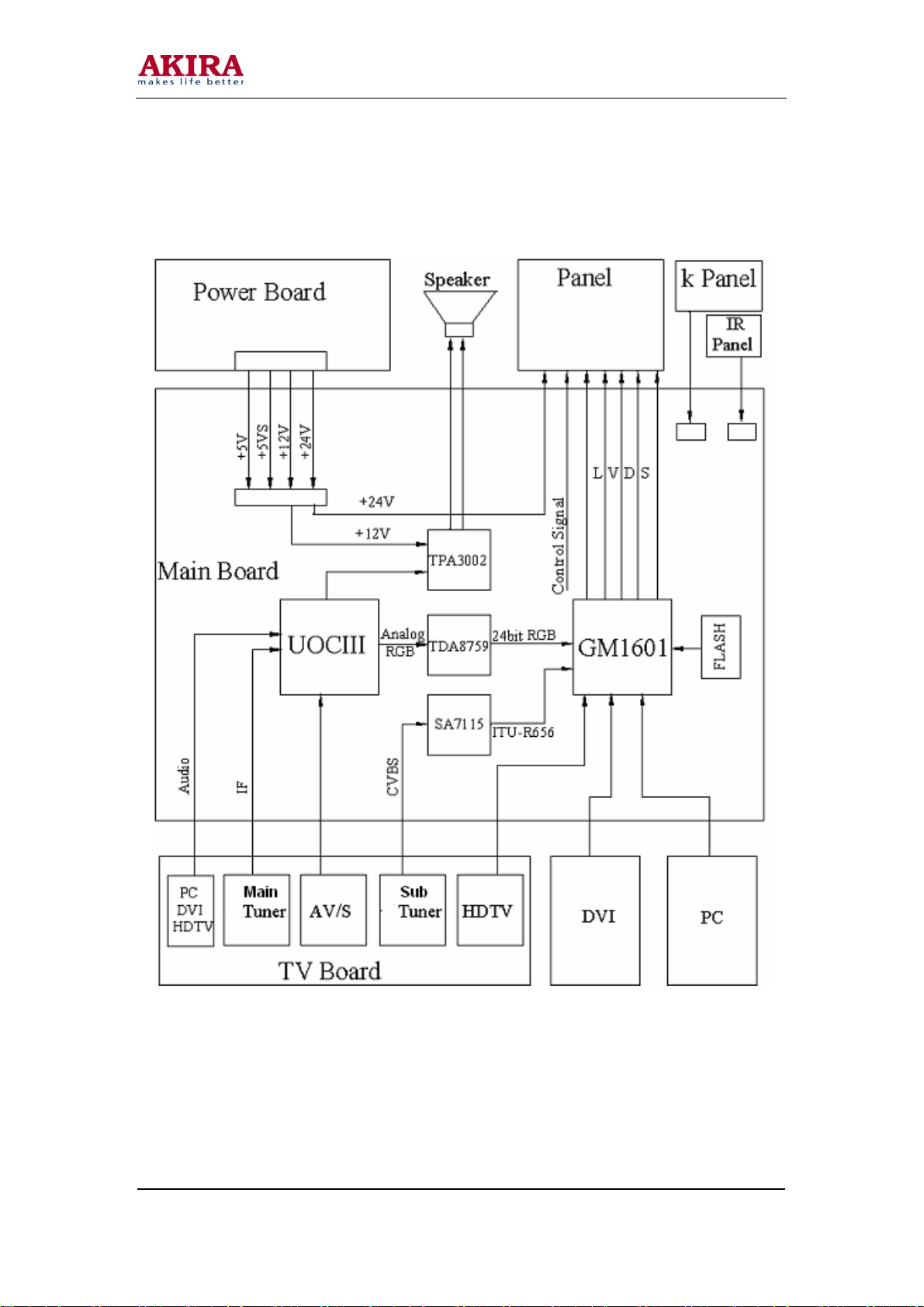
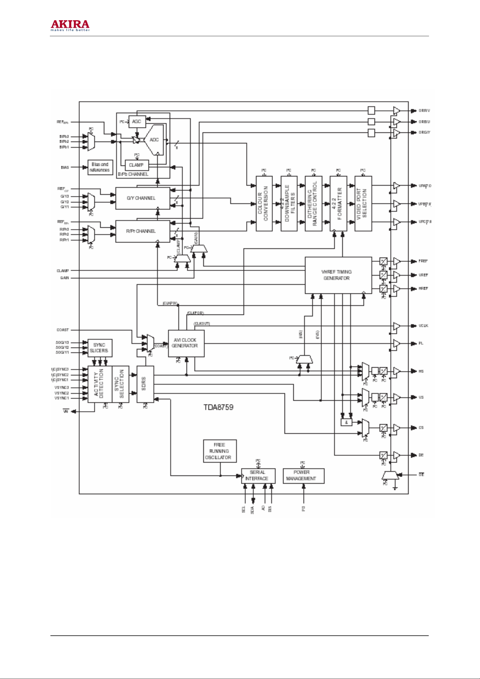
Unit IC Compositions:
LS08 chassis LCD TV is mainly composed of regulator IC, RF IC, video processor IC, Power
Amplify IC, Analog Video IC, System Control IC and Key Control IC, see this IC frame as below:
Model No.: LCT-26CHSTP.doc
Version: 1.0
Page 7
-7 -
PCB Assembly:
It is mainly composed of TV Board、Remote Control Receiver (Signal Receiver), K Board and Main
Board. Hereunder function introduction to every PCB Assembly:
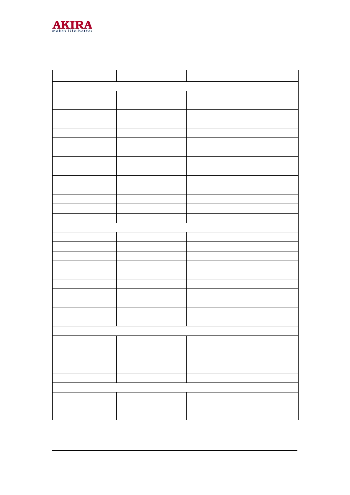
No. Parts Description
1 Main Board
Assembly
2 TV Board
Assembly
3 Remote Control
Receiver
Assembly
4 Built-in Power
Board Assembly
5 K Board
Assembly
6 Screen Assembly Screens for LS08 have built-in adverse transformer, which change DC to
It is the core of signal processing for LCD TV, which takes responsibility
of transforming outer signal into the uniform digital signal identified by
LCD display with use of System Control IC TV and AV signals input from
TV Board are decoded by UOCIII to transport RGB signal which is to be
transformed by TDA8759 modulus to transport 24bit RGB digital signal,
then it is to be transformed by GM1601/GM1501 to produce LVDS signal
displayed on the screen, in addition, signals input from VGA, DVI
would directly enter into GM1501 procedure, format transformation and
on screen display.
It is mainly composed of two tuners (main and sub tuners), AV/S, HD
signal terminals and some peripheral processing IC. The main tuner
demodulates RF signal to IF signal, and the sub tuner produces CVBS
signal, all signals are sent to the main board after transfer.
It is composed of one indicator light and one remote control receiver,
which enable Users operate the TV conveniently and know its current
working status simply with a remote control.
It can transform AC 220V into DC for ICs, including +24V, +12V, +5V
and +5VS power supply in standby mode.
It consists of 7 function buttons by which users can operate the TV freely.
high voltage AC signal lightening the back light; The LCD screen is used
to display the image after the image signal has been processed by the
main board.
Model No.: LCT-26CHSTP.doc
Version: 1.0
Page 8
-8 -
MAIN ICS FUNCTION INTRODUCTION
GENERAL INTRODUCTION
TV Board
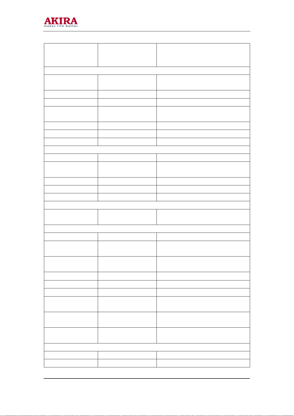
Number Location Type Main Function
1 UT1 TAD5-E2I22RW2 Audio and image intermediate
frequency signal output
2 UT2 TMD2-E49IPWA Sub picture CVBS signal output
Main Board
3 U302, U303 24LC21A T/SN EEPROM
4 U701 24LC32A T/SN Buffer
5 U306, U307,
UA3
6 K201 K3953M Audio surface filter
7 K202 K9656M Audio surface filter
8 U6 TPA3002D2PHPR Audio amplifier
9 U801 AM29LV800DT-70EC
10 U700 GM1501-BD Video processor
11 U201 TDA15021H/N1B07 AV decoder
12 U402 SAA7115HL/V1 Sub channel video decoder
13 U305 SM5302AS-G-ET High definition signal filter
14 U400 TDA8759HV/8/C1 Video signal modulus transformer
15 U5 TDA9178T/N1 Video signal picture amendment
16 U600 MT46V2M32LG-4 Frame buffer
FSAV330QSCX Switch selection
Flash,control program inside
Model No.: LCT-26CHSTP.doc
Version: 1.0
Page 9
-9 -
ICs FUNCTION INTRODUCTION IN DETAILS
Main Tuner (TAD5-E2122RW2)
Pin Definition Description
1 AGC Auto gain control
2 UT NC
3 ADD Ground
4 SCL IIC bus (Clock)
5 SDA IIC bus (Data)
6 NC NC
7 +5V Power supply
8 NC NC
9 30V To produce 0~30V tune voltage
10 NC NC
11 IF Intermediate frequency TV signal
Intermediate frequency TV signal
Sub Tuner (TMD2-E49IPIWA):
Pin Definition Description
1 AGC Auto gain control
2 NC NC
3 ADD Ground
4 SCL IIC bus (Clock)
5 SDA IIC bus (Data)
6 NC NC
7 +5V Power supply
8 NC NC
9 33V To produce 0~30V tune voltage to 0~30V
10 NC NC
11 IF Intermediate frequency output (NC)
12 IF Intermediate frequency output (NC)
13 SW0 Band control
14 SW1 Band control
15 NC NC
16 SIF NC
17 AGC Auto gain control
18 VEDIO CVBS signal output
19 +5V Power supply
20 AUDIO NC
Model No.: LCT-26CHSTP.doc
Version: 1.0
Page 10

-10 -
GM1501
GM1501is a kind of processing chassis for dual channels image and video, which is mainly
used for LCD displays and integrative TV products. With the resolution of WUXGA, it not only
supports PIP technique, but possesses some IC functions applied to image catch, process
and clock display. It integrates high velocity AD converter, PLL, high reliability DVI receiver,
X86 series mic control and LCDS inverter. See the features as below:
Features
High quality image zoom function
Analog RGB signal input interface
Intelligent output signal auto identification
Integrated high-power PLL output
High-reliable self-adaptive DVI input interface
4:4:4/4:2:2/CCR656/601 8/16/24bit digital video interface
Embedded IC for adjustments of gain, contrast, brightness, color saturation, hue and
flesh tone.
Efficiency in reducing EMI electromagnetism inference power consumption
Inclined grain processing with small angle
High quality video processing
Programmable output format
Embedded LVDS transport
Advanced OSD
Embedded micro controller
Model No.: LCT-26CHSTP.doc
Version: 1.0
Page 11
-11 -
Pin Description:
Pin Name Description
Analog signal input port
L3 AVSYNC ADC vertical synchronization signal
input
L4 AHSYNC ADC horizontal synchronization signal
input
N2 VGA-SCL VGA lock input
N1 VGA-SDA VGA digital input
D1, D2 RED+, RED- Red analog signal input
C3 SOG Green synchronization signal
C1, C2 GREEN+, - Green analog signal input
B1, B2 BLUE+, BLUE- Blue analog signal input
A2, B3, E3, D3 ADC3.3 ADC3.3Vpower supply
A3, A4 ADC1.8 ADC1.8Vpower supply
A5, B4 ADC-DGND ADC digital ground
C4, D4, E1, E2, E4 ADC-AGND ADC analog ground
DVI input port
N4 DVI-SCL DDC interface , serial clock signal
N3 DVI-SDA
A6, B6
A8~A10
B8~B10
B11 REXT Exterior cut-off resistance
C6~C11
D6, D8~D10
A7, A11, B5, B7, C7,
D7, D11
Low bandwidth ADC port
C13 LBADC-33 ADC3.3Vpower supply
A12, B12, C12
D12 LBADC_RETURN Channel analog ground
D13 LBADC-GND Power supply voltage analog ground
OCM bus port
AA1~AA3, Y1~Y3,
W1~W3, V1~V4,
U1~U4, T1~T3
RXC+,RXC-
RX0+~RX2+
RX0-~RX2-
DVI-3.3 DVI 3.3V power supply
DVI-1.8 DVI 1.8V power supply
DVI-GND DVI ground
LBADC_IN1~
LBADC_IN3
OCMADDR0~
OCMADDR19
DDC interface ,serial data signal
DVI clock input signal
DVI input port
ADC analog input channel
Address input output port
Model No.: LCT-26CHSTP.doc
Version: 1.0
Page 12
-12 -
AB1~AB3, AC1~AC3,
AD1~AD4, AE1~AE3,
AF1~AF3
OCM port control signal
R1, T4, P1, P2 ROM_CSn~
R2 OCM_REn Read enable signal
R3 OCM_WEn Write enable signal
L1
L2
M1 OCM_UDO OCM data output
M2 OCM_UDI OCM data input
D25 OCM_TIMER1 OCM timer input
Standard definition video control port
D16 SVCLK SV pels clock input
C14 SVHSYNC SV horizontal synchronization signal
B14 SVVSYNC SV vertical synchronization signal input
A14 SVODD Scan status input
A17 SVDV SV data input
Standard definition video data port
D14, D15, A15, A16,
B15, B16, C15, C16
Video Control Port
A20 VCLK Video pels clock signal
D19 VHS_CSYNC Video horizontal synchronization signal
C20 VVS Video vertical synchronization signal
B20 VODD Scan status input
OCMDATA0~
OCMDATA15
ROM_CS2n
OCM_INT2
OCM_INT1
SVDATA7~
SVDATA0
Data input output port
Part selection signal
Interrupt
input
SV ITU656 data input
input
input
D20 VDV (VSOG) Video data input
B17 VCLAMP Video clamp enable output
A21, A22, A23, B21,
B22, C21, C22, D21
C17, C18, C19, A18
A19, B18, B19, D18
B23, B24, B25, A24
A25, C23, C24, D24
Screen Control Port
A26 PPWR Screen power control
B26 PBIAS Screen bias control
Model No.: LCT-26CHSTP.doc
Version: 1.0
VGRN7~ VGRN0 Green signal or Y signal input
VRED7~ VRED0
VBLU7~ VBLU0
Red signal or V/Cr/Pr signal input
Blue signal or U/Cb/Pb signal input
Page 13
-13 -
D26, C25, C26 PWM2 ~PWM0 Pulse width modulation output
AC7 DCLK Pels clock output
AC16 OEXTR Connect external LVDS bias
resistance
LVDS Po rt
AE14~AE16, AE19~
AE23, AF13~AF16
AF19~AF23, AF11
AD14, AD11, AE13
AE11, AC11, AF10
AE12, AF12,
AF20, AE20
Screen Port Power Supply
AD12, AD13, AC12 LVDSB_3.3 LVDS B channel power supply
AC13, AC14, AC15 LVDSB_GND B channel ground
AC20, AC21, AC22 LVDSA_3.3 LVDS A channel power supply
AD19, AC19, AC20 LVDSA_GND A channel ground
AE17 VDDD33_LVDS Analog power supply
AD17 VSSD33_LVDS Analog ground
A0-~A3-, A0+~A3+
B0-~B3-, B0+~B3+
LVDS_SHIELD [5] ~
LVDS_SHIELD [0]
AC+,AC-,BC+,BC- Low voltage difference protect input
Low voltage difference data input
Low voltage difference protect
output
Clock Composite and Power Supply
G4 XTAL Crystal oscillator interface
F2
H1 VDDD33_SDDS
J1 VDDD33_DDDS
G2 VSSD33_PLL
J4 VSSD33_SDDS
K4 VSSD33_DDDS
F4 VDDA33_RPLL
G1 VDDA33_FPLL
H3 VDDA33_SDDS
J3 VDDA33_DDDS
F3 VSSA33_RPLL
H4 VSSA33_FPLL
H2 VSSA33_DDDS
J2 VSSA33_DDDS
G3 TCLK Reference clock signal input
K2 ACS_RSET_HD External resistance port
Model No.: LCT-26CHSTP.doc
Version: 1.0
VDDD33_PLL,
Digital power supply
Digital ground
Analog power supply
Analog ground
Page 14
-14 -
System Signal
K1 RESETn Reset signal
M3, M4
P4 MSTR_SCL Main clock output signal
P3 MSTR_SDA Main data output/input signal
R4 EXTCLK External clock input
Frame Memorizer Interface
U24, U23 FSCLKp, FSCLKn Fine storage clock output
V24, V25 FSRAS, FSCAS Address output
V26 FSWE Write enable port
W26 FSCKE Read enable port
J24 FSVREF Reference voltage input
K26 FSVREFVSS Reference voltage ground
W25 FSVREF Reference voltage input
W24 FSVREFVSS Reference voltage ground
L26 FSDQS Data filter
F24~F26, G23~G26
H24~H26, J25, J26,
R24~R26, P24~P26
N23~N26,
T24, T25, U25, U26 FSDQM3~ FSDQM0 Data output mark
Y26
Y25
AA24~AA26
AB24~AB26,
AC24~AC26
AD24~AD26
E23, F23, H23, J23,
L23, M23, P23, R23,
T23, V23, W23, Y23,
AA23, AB23, AC23
K23 VDDA18_DLL 1.8V power supply
K25 VSSA18_DLL Power supply ground
Digital power supply
K10, K11, K16, K17,
L11, L16, T11, T16,
T17, U10, U11, U16,
U17
IR0,IR1
FSDATA31~ FSDATA0 Data input output port
FSBKSEL1,FSBKSEL0
FSADDR11~
FSADDR0
FS_2.5
CORE_1.8 1.8V power supply
Layer address
Range address output
2.5V power supply
Model No.: LCT-26CHSTP.doc
Version: 1.0
Page 15

-15 -
D23, W4, Y4, AA4,
AB4, AC4, AC6, D17,
D22, AC8, AC10
K12, K13, K14, K15,
L10, L12, L13, L14,
L15, L17, M10, M11,
M12, M13
A1, AC, D5, AC17,
K3, F1
IO_3.3
D_GND
NO_CONNECT
3.3V power supply
Power ground
NC
Model No.: LCT-26CHSTP.doc
Version: 1.0
Page 16

-16 -
GM1501Internal Block Diagram:
Model No.: LCT-26CHSTP.doc
Version: 1.0
Page 17

-17 -
TDA8759:
TDA8759 is a triple 8-bit video converter interface. The IC converts a RGB analog signal into
a 24bit RGB or YUV or YCbCr digital signal or converts a YUV or YCbCr analog signal into a
YUV or RGB digital signal with a sampling rate up to 81 Msps. The IC supports resolutions
from 480i and VGA to HDTV and XGA.
Features
Triple 8-bit Analog-to-Digital Converter (ADC)
Three independent analog video sources up to 81 Msps selectable by I2C-bus
Auto check on interval scan video signal
1.8Vand 3.3Vsupplies
Low gain variation with temperature
Output format RGB 4:4:4, YUV 4:4:4, YUV 4:2:2, CCIR 656 or YUV 4:2:2 semi-planar
standard on output bus
I²C bus control
Programmable clock phase adjustment cells
Amplifier bandwidth of 100 MHz
Integrated PLL divider
Power-Down mode
Model No.: LCT-26CHSTP.doc
Version: 1.0
Page 18
-18 -
TDA8759 Block Diagram
Model No.: LCT-26CHSTP.doc
Version: 1.0
Page 19
-19 -
Pin Description:
Pin Name Description
1 HREF Horizontal reference output
2 VCLK Video clock output
3, 13, 21, 29,
37, 45, 164
4, 14, 22, 30
38, 46, 165
7, 8, 9, 10, 15,
16, 17, 18
11, 116, 130, 132 VDDC Power supply port
12, 117, 159 CGND Ground
23~28, 31, 32 VPB0~VPB7 Video port B
35, 36, 39~44 VPC0~VPC7 Video port C
47, 53, 57, 58, 55
60, 66, 70, 71, 75
81, 83, 85, 86,
48, 54, 59, 61, 67
69, 76, 82, 85,
87, 88
49 REFB/Pb Blue/blue-chrominance channel reference
52, 51, 50 B/Pb1~ B/Pb3 Blue/blue-chrominance channel analog input
56 BIAS Bias input
62 REFG/Y Green/green-chrominance channel reference
65,64,63 G/Y1~G/Y3 Green/green-chrominance channel analog
74,73,72 SOG/Y1~SOG/Y3 Sync on green//brightness channel input
77 REFR/Pr Red/red-chrominance channel reference input
80,79,78 R/Pr1~ R/Pr3 Red/red-chrominance channel analog input
89~92,97~101
112,121,122,
124,125,160~163
93 PD Power-down control input
94 OE Output enable input
96 A0 I²C bus address control input
102 COAST PLL control input
103 GAIN Gain input
104 CLAMP Clamp input
VDDO Video port output supply voltage
OGND Video port output
ground
VPA0~VPA7 Video port A
AGND Analog ground
VDDA Power supply port
input
input
input
TST0~TST17 Reserved for test
Model No.: LCT-26CHSTP.doc
Version: 1.0
Page 20
-20 -
105~107 VSYNC1~VSYNC3 Vertical synchronization input
108~110 H(C)SYNC1~
H(C)SYNC3
111 CKEXT External clock input
113 TCLK Reserved for test
114 DIS I²C bus disable control input
118 SDA I²C bus data input/output
119 SCL I²C bus clock input
120, 126, 127,
131
133, 142, 148,
123, 138, 139,
145
151, 157
166 PL PLL disable output
167 DE Data enable output
168 HS Horizontal synchronization input
169 VS Vertical synchronization input
170 CS Color synchronization output
171 ORR/V Red / chrominance ADCoutput
172 ORB/U Blue /chrominance ADCoutput
173 ORG/Y Green / chrominance ADCoutput
174 VAI Video dynamic indication output
175 FREF Scan output
17 VREF Vertical channel reference input
TPA3002D2:
The TPA3002D2 is a 9-W (per channel) efficient, Class-D audio amplifier for driving bridged-tied
stereo speakers. The TPA3002D2 can drive stereo speakers as low as 8. The high efficiency of the
TPA3002D2 eliminates the need for external heat sinks when playing music.
Features:
9W /Ch into an 8Ω load from 12Vsupply;
Efficient, class D operation eliminates heat sinks and reduces power supply requirements;
32-step DC volume control from -40db~36db;
Line outputs for external headphone;
Thermal and short-circuit protection
IGND Input digital ground
VDDI Input digital supply voltage
Horizontal (composite) synchronization input
Model No.: LCT-26CHSTP.doc
Version: 1.0
Page 21
-21 -
Pins Functions:
Pin Name Description
26, 30 AGND Analog ground for digital/analog cells in core
33 AVCC
29 AVDD 5V regulated output capable of 100mA output
7 AVDDREF Reference 5V output
13 BSLN
24 BSLP
48 BSRN
37 BSRP
28 COSC I/O for charge/discharge currents onto capacitor for ramp
6 LINN
5 LINP
16,17
20,21
34 MODE Input for MODE control. A logic high on this pin places the
35 MODE_OUT Output for control of the variable output amplifiers. When the
18,19,42
,43
14,15,22
,23
38,39,46
,47
LOUTN
LOUTP
PGNDR, PGNDL Power ground for left channel H-bridge Power ground for
PVCCL
PVCCR
High-voltage analog power supply(8~14V)
Bootstrap I/O left channel
Bootstrap I/O right channel
generator triangle
Negative differential audio input for left channel
Positive differential audio input for left channel
Class-D 1/2-H-bridge negative output for left channel
Class-D 1/2-H-bridge positive output for left channel
amplifier in the variable output mode and the Class-D
outputs are disabled. A logic low on this pin places the
amplifier in the Class-D mode and Class-D stereo outputs
are enabled. Variable outputs (VAROUTL and VAROUTR)
are still enabled in Class-D mode to be used as line-level
outputs for external amplifiers.
MODE pin (34) is a logic high, the MODE_OUT pin is driven
low. When the MODE pin (34) is a logic low, the MODE_OUT
pin is driven high. This pin is intended for MUTE control of an
external headphone amplifier. Leave unconnected when not
used for headphone amplifier control.
right channel H-bridge
Power supply for left channel H-bridge (tied to pins 22 and
23 internally), not connected to PVCCR or AVCC.
PVCCL 22, 23 – Power supply for left channel H-bridge (tied
to pins 14 and 15 internally), not connected to PVCCR or
AVCC.
PVCCR 38,39 – Power supply for right channel H-bridge
(tied to pins 46 and 47 internally), not connected to PVCCL
or AVCC.
PVCCR 46, 47 – Power supply for right channel H-bridge
(tied to pins 38 and 39 internally), not connected to PVCCL
or AVCC.
Model No.: LCT-26CHSTP.doc
Version: 1.0
Page 22

-22 -
12 REFGND Ground for gain control circuitry. Connect to AGND. If using
a DAC to control the volume, connect the DAC ground to this
terminal.
32 RINP
2 RINN
27 ROSC Current setting resistor for ramp generator. Nominally equal
44, 45,
40, 41
1 SD Shutdown signal for IC (low = shutdown, high = operational).
9 VARDIFF DC voltage to set the difference in gain between the Class-D
10 VARMAX DC voltage that sets the maximum gain for the VAROUT
31 VAROUTL Variable output for left channel audio. Line level output for
32 VAROUTR VAROUTR 32 O Variable output for right channel audio. Line
25 VCLAMPL VCLAMPL 25 – Internally generated voltage supply for left
36 VCLAMPR Internally generated voltage supply for right channel
11 VOLUME DC voltage that sets the gain of the Class-D and VAROUT
8 VREF Analog reference for gain control section.
4 V2P5 2.5-V Reference for analog cells, as well as reference for
ROUTN, ROUTP Class-D 1/2-H-bridge negative output for right channel
Positive differential audio input for right channel
Negative differential audio input for right channel
to 1/8*
ROUTP 40, 41 O Class-D 1/2-H-bridge positive output for
right channel
TTL logic levels with compliance to VCC.
and VAROUT outputs. Connect to GND or AVDDREF if
VAROUT outputs are unconnected.
outputs. Connect to GND or AVDDREF if VAROUT outputs
are unconnected.
driving external HP amplifier.
level output for driving external HP amplifier.
channel bootstrap capacitors.
bootstrap capacitors.
outputs.
unused audio input when using single-ended inputs.
Model No.: LCT-26CHSTP.doc
Version: 1.0
Page 23

-23 -
TPA3002D2 External Block Diagram:
Model No.: LCT-26CHSTP.doc
Version: 1.0
Page 24

-24 -
SM5301AS:
Order Butterworth low pass filter configuration. The filter characteristics have been optimized for
minimal overshoot and flat group delay, it has a variable cutoff frequency and guaranteed driver-stage
channel gain difference and phase difference values.
Features:
Supply voltage:5V±10%;
DC voltage level restore sync clamp function
Output buffer gain switching function: 0, 6dB (input-to-output AC signal gain)
Channel-to-channel gain difference: 0.5dB(±5% supply voltage variation)
Channel-to-channel phase difference: 3.5 degree
Output signal harmonic distortion (all channels): 1.5%
Cutoff frequency: 5.8 to 37MHz variable
SM5301AS Internal Block Diagram:
Model No.: LCT-26CHSTP.doc
Version: 1.0
Page 25

-25 -
Pin Description:
Pin Name Description
2 GSG1 GOUT/UOUT output buffer gain set input
1 GINA/UINA
3 GINB/UINB
5 BINA/VINA
7 BINB/VINB
6 GSB1 BOUT/VOUT output buffer gain set input
9 DISABLE Power save function. Built-in pull-down resistor.
10, 13, 16,
19
11 BOUT/VOUT B/V signal output
14 GOUT/UOUT Analog 5V supply
17 ROUT/YINB R/Y signal output
12, 15, 18,
24
20 RFC LPF (low pass filter) cutoff frequency setting resistor
21 VFC LPF (low pass filter) cutoff frequency setting voltage input
22 MUXSEL Input select signal
23 SYNCIN Filter channel external H-Sync signal input.
26 GSR1 ROUT/YOUT output buffer gain set input
25 RINA/YINA
27 RINB/YINB
4, 8, 28 NC No connection (leave open or connect to ground)
Model No.: LCT-26CHSTP.doc
Version: 1.0
GND Ground
VCC Analog 5V supply
Analog GINA or UINA signal input. Sync signal is input on
SYNCIN pin.
Analog GINB or UINB signal input. Sync signal is input on
SYNCIN pin.
Analog BINA or VINA signal input. Sync signal is input on
SYNCIN pin.
Analog BINB or VINB signal input. Sync signal is input on
SYNCIN pin
connection
Analog RINA or YINA signal input. Sync signal is input on
SYNCIN pin.
Analog RINB or YINB signal input. Sync signal is input on
SYNCIN pin.
Page 26

-26 -
SAA7115:
The SAA7115 is a video capture device for various applications ranging from small screen
products like e.g. digital set top boxes, personal video recording applications to big screen
devices like e.g. LCD projectors due to it’s improved comb filter performance and 10 bit video
output capabilities.
Features
Six analog inputs, internal analog source selectors;
Two improved 9 Bit CMOS analog-to-digital converter in differential CMOS style;
Automatic Clamp Control (ACC) for CVBS, Y and C;
Enhanced Horizontal and vertical Sync Detection;
PAL delay line for correcting PAL phase errors;
Automatic TV/VCR detection; TV/VCR
Model No.: LCT-26CHSTP.doc
Version: 1.0
Page 27

SAA7115 Internal Diagram:
-27 -
Model No.: LCT-26CHSTP.doc
Version: 1.0
Page 28

-28 -
Pin Function:
Pin Name Description
1,8,11,17,23,25,33
43,51,58,68,75,83
93
2 TDO Test Data Output for Boundary Scan Test (2)
3 TDI Test Data Input for Boundary Scan Test (with internal
4 XTOUT Crystal oscillator output signal, auxiliary signal
VDD Supply voltage port
pull-up)(2)
6 XTALO
7 XTALI
6 VXDD Crystal oscillator power supply
10,12,14,16 AI21~AI24 Analog signal input
13 AI2D
19 AI1D
20 AI11
18 AI12
5,9,15,21,24,26,38
50,63,76,88,100
22 AOUT Analog test output (do not connect)
27 CE Chip Enable or RESET input (with internal pull up)
28 LLC
29 LLC2
30 RESON RESet Output Not signal
31 SCL IIC serial clock line (with inactive output path)
32 SDA IIC serial data line
34 RTS0
35 RTS1
36 RTCO Real time control output
AGND
VSS
24.576 (32.11) MHz crystal oscillator output; not
connected if XTALI is driven by an external single-ended
oscillator.
Input terminal for 24.576 (32.11) MHz crystal oscillator or
connection of external oscillator with TTL compatible
square wave clock signal.
Differential input for ADC channel 2 (pins AI24, AI23,
AI22, AI21) differential input for ADC channel 1 (pins
AI12, AI11)
Analog input 11
Analog input 12
Ground
Line-locked system clock output (27 MHz nominal), for
backward compatibility, do not use for new applications
line locked clock/2 output (13.5 MHz nominal) for
backward compatibility, do not use for new applications
Real time status or sync information, controlled by
subaddr. “11h and 12h” RTS1 35 O real time status or
sync information, controlled by subaddr. “11h and 12h”
37 AMCLK Audio master clock output
39 ASCLK Audio serial clock output
Model No.: LCT-26CHSTP.doc
Version: 1.0
Page 29

-29 -
40 ALRCLK Audio lift/right clock output
41 AMXCLK Audio master external clock input
42 ITRDY Target ready input, image port (with internal pull up)
45 ICLK Clock output signal for image-port, LCLK of LPB image port
mode, or optional asynchrony backend clock input
46 IDQ Output data qualifier for image port (optional: gated clock
output)
47 ITRI Image-port output control signal, effects all I-port pins incl.
ICLK, enable and active polarity is under software control
(bits IPE in subaddr. “87”) output path used for Testing:
scan output
48 IGP0
49 IGP1
52 IGPV Multi purpose vertical reference output signal; image-port
53 IGPH Multi purpose horizontal reference output signal;
54~57,59~62 IPD0~IPD7 Image port data output
General purpose output signal 0; image-port (controlled by
subaddr. “84”,”85”)
General purpose output signal 1; image-port (controlled by
subaddr. “84”,”85”),
same functions as IGP0
(controlled by subaddr. “84”,”85”)
image-port
(controlled by subaddr. “84”,”85”)
64~67,69~72 HPD0~HPD7 Host port data I/O, carries UV chrominance information in
16 bit video I/O modes
80 XTRI X-port output control signal, effects all X-port pins
(XPD[7:0], XRH, XRV, XDQ and XCLK) enable and active
polarity is under software control (bits XPE in subaddr.
“83”)
81,82,84,85,
89,90,86,87
91 XRV vertical reference I/O expansion-port:
92 XRH horizontal reference I/O expansion-port:
94 XCLK clock I/O expansion port
95 XDQ data qualifier I/O expansion port
96 XRDY task flag or read signal from scaler, controlled by XRQT
XPD0~XPD7 expansion-port data
expansion-port data
In ten bit video output mode: this signal represents the
video bit 0.
In ten bit video output mode: this signal represents the
video bit 1.
(subaddr. 83H)
Model No.: LCT-26CHSTP.doc
Version: 1.0
Page 30

-30 -
97 TRSTN Test ReSeT Not for Boundary Scan Test (with internal
pull-up); for board design without Boundary Scan connect
TRSTN to ‘ground’ (1)
98 TCK Test Clock for Boundary Scan Test (with internal pull-up)
(2)
99 TMS Test Mode Select for Boundary Scan Test or Scan Test
(with internal pull-up) (2)
UOC (TDA15021h):
The UOCIII series combines the functions of a Video Signal Processor (VSP) together with a
FLASH embedded TEXT/Control/Graphics -Controller (TCG -Controller) and US Closed
Caption decoder.
Features
DVB/VSB IF circuit for preprocessing of digital TV signals;
Video switch with 3 external CVBS inputs and a CVBS output;
Automatic Y/C signal detector;
Adaptive digital (4H/2H) PAL/NTSC comb filter for optimum separation of the luminance
and the chrominance signal;
Picture improvement features with peaking (with switchable center frequency, depeaking,
variable positive/negative peak ratio, variable pre-/overshoot ratio and video dependent
coring), dynamic skin tone control, gamma control and blue and black stretching. All
features are available for CVBS, Y/C and RGB/YPBPR signals.
The mono intercarrier sound circuit has a selective FM-PLL demodulator which can be
switched to the different FM sound frequencies (4.5/5.5/6.0/6.5 MHz). The quality of this
system is such that the external band-pass filters can be omitted. In the stereo versions of
UOCIII the use of this demodulator is optional for special applications.
Normally the FM demodulators of the stereo demodulator/decoder part are used (see
below).
The FM-PLL demodulator can be set to centre frequencies of 4.72/5.74 MHz so that a
second sound channel can be demodulated. In such an application it is necessary that an
external band pass filter is inserted.
The vision IF and mono intercarrier sound circuit can be used for the demodulation of FM
radio signals. With an external FM tuner also signals with an IF frequency of 10.7 MHz can
be demodulated. For the QIP90 versions this is valid only for the “stereo” versions
Built-in adaptable brightness delay circuit
Switch able brightness signal transmission rate
Model No.: LCT-26CHSTP.doc
Version: 1.0
Page 31

-31 -
Pin Description:
Pin Name Description
1,2,12,18,28,40
68,81,89,92,95,1
01
121,125
3,4,45,69,82,88,
90,
91,93,94,96,100,
110,117,118,124
5 VREF_POS_LSL
6 VREF_NEG_LSL+HPL
7 VREF_POS_LSR+HP
8 VREF_NEG_HPL+HP
9 VREF_POS_HPR
10 XTALIN Crystal oscillator input
VSS, GND Ground
VDD Power supply
SDAC input signal
R
R
11 XTALOUT Crystal oscillator output
13 VGUARD/SWIO V-guard input / I/O switch
14 DECDIG decoupling digital supply
15 VP1 decoupling digital supply
16 PH2LF
17 PH1LF
19 SECPLL
20 DECBG
21 EWD/AVL East-West drive output or AVL capacitor
22 VDRB
23 VDRA
24 VIFIN1
25 VIFIN2
27 IREF reference current input
29 SIFIN1/DVBIN1
30 SIFIN2/DVBIN2
31 AGCOUT tuner AGC output
32 EHTO EHT / overvoltage protection input
33 AVL/SWO/SSIF/REFO
/REFIN
34 AUDIOIN5L
35 AUDIOIN5R
phase-2 filter
phase-1 filter
SECAM PLL decoupling
bandgap decoupling
vertical drive B output
vertical drive A output
IF input 1
IF input 2
SIF input 1 / DVB input 1
Automatic Volume Levelling / switch output
reference output / external reference signal
DVB operation
audio-5 input (left signal)
audio-5 input (right signal)
Model No.: LCT-26CHSTP.doc
Version: 1.0
Page 32

-32 -
Pin Name Description
36 AUDOUTSL
37 AUDOUTSR
38 DECSDEM decoupling sound demodulator
39 QSSO/AMOUT/AUDEEM QSS intercarrier output / AM output / deemphasis
41 PLLIF PLL filter
42 SIFAGC/DVBAGC AGC sound IF / internal-external AGC for DVB
43 DVBO/IFVO/FMRO
44 DVBO/FMRO
46 AGC2SIF AGC capacitor second sound IF
47 VP2 2nd supply voltage TV processor (+5 V)
48 IFVO/SVO/CVBSI video output / selected CVBS output / CVBS
49 AUDIOIN4L
50 AUDIOIN4R
audio output for SCART/CINCH (left signal)
audio output for SCART/CINCH (right signal)
SCART
QSS
applications
Digital Video Broadcast output / IF video output
audio-4 input (left signal)
audio-4 input (right signal)
51 CVBS4/Y4 CVBS/Y input
52 C4 chroma-4 input
53 AUDIOIN2L/SSIF
54 AUDIOIN2R
56 AUDIOIN3L
57 AUDIOIN3R
30 AUDOUTLSL
61 AUDOUTLSR
62 AUDOUTHPL
63 AUDOUTHPR
58 CVBS3/Y3 CVBS/Y input
59 C2/C3 chroma-2/3 input
55 CVBS2/Y2 CVBS/Y input
64 CVBSO/PIP CVBS/PIP signal output
65 SVM scan velocity modulation output
66 FBISO/CSY flyback input/sandcastle output or composite H/V
67 HOUT horizontal output
70 VIN (R/PRIN2/CX) V-input for YUV interface
71 UIN (B/PBIN2) U-input for YUV interface
Audio input
Model No.: LCT-26CHSTP.doc
Version: 1.0
Page 33

-33 -
Pin Name Description
72 YIN
(G/YIN2/CVBS-YX)
73 YSYNC Y-input for sync separator
74 YOUT Y-output (for YUV interface)
75 UOUT (INSSW2) U-output for YUV interface
76 VOUT (SWO1) V-output for YUV interface
77 INSSW3 3rd RGB / YPBPR insertion input
78 R/PRIN3 3rd R input / PR input
79 G/YIN3 G input / Y input
80 B/PBIN3 3rd B input / PB input
83 BCLIN Beam current limiter input
85 RO Red output
86 GO Green output
Y-input for YUV interface
87 BO Blue output
97 INT0/P0.5 External interrupt 0 or port 0.5 (4 mA current
sinking direct drive of LEDs)
98,99,102~109
111~116,119,120
122,123,126~ 128
P0.0~ P0.4
P1.0~P1.7,P2.0~P2.5,
P3.0~P3.3
Data port
Model No.: LCT-26CHSTP.doc
Version: 1.0
Page 34

-34 -
UOC Block Diagram:
CHAPTER THREE
SIGNAL FLOW ANALYSIS AND KEY POINT MEASURE DATA
Model No.: LCT-26CHSTP.doc
Version: 1.0
Page 35

-35 -
The chapter mainly introduces the receipt and dispose of the AV signal, the power supply
system and system control process of this TV.
Video Signal Flow:
The IF signal which is demodulated from RF signal by main demodulator is sent through TV
board into video decode chassis UOC for decoding, together with the input signals via AV
port and two-way SCART ports, then the output analog video signal is sent into
analog-to-digital converter TDA8759HV/8/C1 for A/D transform to produce R, G, B digital
signals which are transformed in format by GM1601/GM1501, then, it transformed the
different input formats into the uniform up-screen signal format. In addition, that TV signal is
processed by UOC would produce two-way CVBS signal respectively used for video output
of two-way SCART and AV ports.
The signal demodulated from RF signal by sub demodulator is directly sent into submenu
video decoder SAA7115HL/V1 for video decoding and A/D conversion, together with the
input signals via AV port and two-way SCART ports, then again sent into GM1601/GM1501 to
do format transform, the output up-screen is used for submenu display.
The alternative PC, HDTV (YPBPR) and DVI signals are sent directly into GM1601/GM1501
for processing to form uniform up-screen signal.
Accompanying Sound Flow:
What input sound signal would be sent into UOC for demodulation and sound disposal after
selection and simple processing then, the output audio signal is zoomed in by D class
TPA3002D2PHPR and is sent into the speaker at last. The other is used for SCART and AV
sound output.
TV Power Supply System:
4 channels voltage is transported from the power supply board, they are +24V, +12V, +5V
and +5VS. +24V is provided for inverter of LCD panel, +12V is provided for PA, +5V is
transformed by the DO (for example: LM1117, LM1084) into 3.3V, 2.5V and 1.8V for IC, it
may be turned down under standby mode, while +5VS is provided for MCU, infrared receiver,
EEPROM.
5V is divided into two ways, one way is provided for other IC and apparatus, the 5V will be
turned down under standby mode, but can not be cut off. The other 5V is provided for MCU,
infrared receiver, EEPROM and so on, it would not be cut off under standby mode.
Model No.: LCT-26CHSTP.doc
Version: 1.0
Page 36

-36 -
p
p
p
,
JP1 9,
1C PIN
12 V
JP11 9,
2 PIN
U3 MC78M08
U501 LM2596-5.0
UP3 IRF7134
UP7
LM1117-1.8
UP6
LM2596-5.0
JP3 the 9th PIN
arent/sub TUNER
JP11 7,
8 PIN
24V
UA3 the 16th PIN
th
UA1 the 14
PIN
U503
LM1084IS-3.3
U502
LM2596-5.0
U504
LM1117-1.8
JP1 the
th
PIN
6
MCU5
U505
LM1117-2.5
U506
LM1117-3.3
Model No.: LCT-26CHSTP.doc
Version: 1.0
U5 TDA9178
th
The 20
The 26-30
U6 TPA3002
14, 15, 22, 23, 33,
38, 39, 46, 47 pin
in
JP701
th
in
U201 UOCIII 100, 11,
7, 124, 15, 3, 118, 96,
93
U400 TDA8759 13, 64,
21, 29, 37, 43, 138, 3, 139,
145, 151, 157, 123 PIN
U402 SAA7115 1, 25, 51,
75, 33, 43, 58, 68, 93, 8, 83
U700 GM1601
U305 the 2nd PIN
CN70 the 4
CN70 the 3
47, 82 PIN
PIN
th
PIN
rd
PIN
Page 37

-37 -
N
Manostat Pin Voltage in Main Board Schedule
JP1 4, 5
PI
U508 IRF7134
U403
LM1117-1.8
U405
LM1117-3.3
Name Type PIN1(V) PIN2(V) PIN3(V) PIN4(V) PIN5(V)
UP7 LM1117-1.8V 0 1.8 5 1.8
UP1 LM1117-3.3V 0 3.3 5 3.3
UP6 LM2596-5.0 24 5 0 5 0
U405 LM1117-3.3 0 3.3 5 3.3
U3 78M08 12 0 8
U403 LM1117-1.8V 0 1.8 5 1.8
U503 LM1806-3.3 0 3.3 5 3.3
U505 LM1117-2.5 0 2.5 5 2.5
U506 LM1117-3.3 0 3.3 5 3.3
U501 LM2596-5.0 12 5 0 5
U502 LM2596-5.0 24 5 0 5 0
U504 LM1117-1.8V 0 1.8 5 1.8
U309
NLAS4052 the
th
PIN
16
U305 SM5301
18, 22, 26 PIN
U400 TDA8759 11,
87, 16, 30, 32, 58 PIN
U400 TDA8759 88, 48,
54, 61, 67, 69, 76, 82,
59 PIN
Model No.: LCT-26CHSTP.doc
Version: 1.0
Page 38

-38 -
Main Components and Socket Locations and Definitions:
Model No.: LCT-26CHSTP.doc
Version: 1.0
Page 39

-39 -
Outlet Definition:
Number Name Connected Object Function Description
1 JP400
JP401
2 JP2 Side AV
3 JP6 DVD AV output
4 JP7 Speaker
5 JP8 Speaker
6 JP4 DVD decode board
7 JP3 Outside AV input
8 JP9 Up screen (screen
9 JP10 Up screen (screen
10 JP12 Power supply board GND, GND, GND, +12V, +12V, +12V
11 J171 Prepare to use
13 JP11 Power supply board +12V, +12V, GND, GND, GND, GND, 24V,
14 JP1 Power supply board SB, GND, GND, 5V, 5V, 5V, GND, GND,
15 J700 Prepare to use
16 CN702 Prepare to use
17 CN700 Remote control
18 CN701 K board
19 CN304 Prepare to use
20 CN303 Prepare to use
21 JP701 Display
22 CN306 Prepare to use
23 AVP303 DVI audio input
24 CN300 DVI port
TV board
inverter input)
inverter input)
24V
12V, 12V
25 AVP300 VG audio input
26 CN301 VGA port
27 JPY400
JPY401
JPY402
28 JPA400 SCART (1) interface
29 JPA401 SCART (2) interface
Model No.: LCT-26CHSTP.doc
Version: 1.0
HDTV AV input
Page 40

-40 -
Main Components Description:
Number Name Components Function Description
A U201 TDA15021H/N1B07 AV decoder
B U400 TDA8759HV/8/C1 Video signal AD converter
C U402 SAA7115HL/V1 Sub channel video decoder
D U600 MT46V2M32LG-4 Frame buffer memorizer
E U700 GM1601/GM1501-BD Video processor
F U305 SM5302AS-G-ET HD signal filter
G U801 AM29LV800DT-70EC
H U6 TPA3002D2PHPR Audio PA
I U5 TDA9178T/N1 Video signal image improve
J K202 K9656M Sound surface filter
K K201 K3953M Sound surface filter
L UA3 FSAV330QSCX Select switch
M U701 24LC32A T/SN Buffer
N U307 FSAV330QSCX Select switch
O U306 FSAV330QSCX Select switch
P U302 24LC21A T/SN EEPROM
Q U303 24LC21A T/SN EEPROM
Flash,the TV control procedure put in it
Model No.: LCT-26CHSTP.doc
Version: 1.0
Page 41

-41 -
Main Points Undulance Illustrations:
RF input color stripe signal, TV signal undulance in the 19
th
of SAA7115 also like this:
the 10
th
pin of sub tuner UT1,The undulance of
RF input color stripe signal, the Pin85, Pin86, Pin87 of U201 output R,G,B signal undulance, the E
pole undulance of Q171,Q172,Q173:
Model No.: LCT-26CHSTP.doc
Version: 1.0
Page 42

-42 -
RF input color stripe signal, I²C bus clock signal UOCIII_SCL, the undulance of the 98
th
pin of U5, the 4th pin of parent/sub RF tuner:
the 11
th
pin of U201,
RF input color stripe signal, UOC vertical sync signal, the undulance of the 22th pin of U201, the
th
pin of U400:
105
Model No.: LCT-26CHSTP.doc
Version: 1.0
Page 43

-43 -
RF input color stripe signal
th
pin of U400:
105
,UOC vertical sync signal , the undulance of the 22th pin of U201,the
Model No.: LCT-26CHSTP.doc
Version: 1.0
Page 44

-44 -
RF input gray ladder signal, the TV signal undulance in the 19
th
pin of SAA7115:
The 1KHz sound signal input, the undulance of the 60th, 61th pin of U201, the undulance of the 2th,
th
pin of U6 also like this:
6
Model No.: LCT-26CHSTP.doc
Version: 1.0
Page 45

-45 -
th
The 1KHz sound signal input, the undulance of 16
pins:
Location
No.
UP7 LM1117-1.8V 0 1.8 5 1.8
UP1 LM1117-3.3V 0 3.3 5 3.3
UP6 LM2596-5.0 24 5 0 5 0
U405 LM1117-3.3 0 3.3 5 3.3
U3 78M08 12 0 8
U403 LM1117-1.8V 0 1.8 5 1.8
U503 LM1806-3.3 0 3.3 5 3.3
U505 LM1117-2.5 0 2.5 5 2.5
U506 LM1117-3.3 0 3.3 5 3.3
U501 LM2596-5.0 12 5 0 5
U502 LM2596-5.0 24 5 0 5 0
U504 LM1117-1.8V 0 1.8 5 1.8
Type PIN1(V) PIN2(V) PIN3(V) PIN4(V) PIN5(V)
, 17th, 20th , 2140th , 41th, 44th, 45th pin of U6 and
Model No.: LCT-26CHSTP.doc
Version: 1.0
Page 46

-46 -
SYMPTOMS AND CORRECTION
Symptom Reason and resolve
The display board of PC no
image in DVI.
No picture but sound, on
LOGO when turning on the
TV, poor light is bright.
No picture, no sound, no
snowflake in TV condition,
but AV is normal.
LCD TV can not be
controlled (inc red lamp is
no but the TV is off, remote
control and key press in TV
can not control the TV, etc.)
If some display board of DVI can not receive the data when turning
on the TV, there is no output; if pull out the DVI line abruptly, there
is also no DVI output; Before starting PC, connect the DVI line with
LCD TV steadily. So DVI can receive the correct date from DDC
(Display Data Channel) when turning on the TV, DDC is in chassis
24LC21.
Check the connect line in up screen, and connect the line.
Check the outside of RF (also bus and power supply), there is no
problem but no output from RF, so the RF is disabled.
The LCD TV can not work abruptly, power off and turning it on
again.
Model No.: LCT-26CHSTP.doc
Version: 1.0
Page 47

-47 -
LISTS OF BREAKABLE AND MAINTENANCE PARTS
This list is provided for reference, if change the parameters of those maintain parts of an apparatus, we do
not notice in the future. The newest data regard as the correct type or specification.
27″series:
Breakable
No Name Code Number PCB Number
1. Frame 8807400310J JUJ8.074.031 0.1
2. Suspend screen 8864000190J JUJ8.640.019 0.1
3. Back cover 8807400341J JUJ8.074.034-1 0.1
4. Base decorate board 8735600050J JUJ7.356.005 0.1
5. Base 8807000130J JUJ8.070.013 0.1
6.
Main board assembly 8669000353J JUJ6.690.035-3
7.
AV board assembly 8669300150J JUJ6.693.015
8.
TV board assembly 8669700040J JUJ6.697.004
Remote receive
9.
board assembly 8669400180J JUJ6.694.018
Key press board
10.
assembly 8669400190J JUJ6.694.019
Inside power supply
11.
module 67128017905 FSP179-4F01 5
12. LCD display screen 68219602735 V270W1-L04 0.1
13. Electron tuner 8289100063E TMI4-C22P2RW 1
14. Electron tuner 8289100454E TAD5-C2IP1RW 1
15. Electric speaker 56224605080 Y2929-01-5W-8Ω 2
16.
Electric speaker 562D6608082
17. Remote controller 8201803760L KLC5A 1
Y50138-01-8W-8
Ω 2
PCB
JUJ7.820.088 1
PCB
JUJ7.820.103 0.5
PCB
JUJ7.820.128 1
PCB
JUJ7.820.104 0.5
PCB
JUJ7.820.091 0.5
Proportion
(%)
Model No.: LCT-26CHSTP.doc
Version: 1.0
Page 48

-48 -
37″series:
Breakable
No Name Code Number PCB Number
1
Frame
2
Back cover
3
Base
4
Main board assembly
5
AV board assembly
6
TV board assembly
Remote receive
7
board assembly
Key press board
8
assembly
Inside power supply
15
module
16
LCD display screen
17
Electron tuner
18
Electron tuner
19
Electric speaker
20
Electric speaker
21
Remote controller
22
Remote emitter
8807400430
J JUJ8.074.043
8807400442
J JUJ8.074.044-2
8807000160
J JUJ8.070.016
8669000354
J JUJ6.690.035-9
8669300150
J JUJ6.693.015
8669700040
J JUJ6.697.004
8669400200
J JUJ6.694.020
8669400240
J JUJ6.694.024
6821370010
5 LC370W01 0.1
8864000150
J JUJ8.640.015 0.1
8289100063
E TMI4-C22P2RW 1
8289100454
E TAD5-C2IP1RW 1
5623297108
1 Y3297-L-10W-8Ω 1
5623297108
2 Y3297-R-10W-8Ω 1
5623939058
0 Y3939-01-5W-8Ω 2
8201803510
L KLC5B 1
JUJ7.820.088 1
JUJ7.820.103 0.5
JUJ7.820.128 1
JUJ7.820.104 0.5
JUJ7.820.091 0.5
0.1
0.1
0.1
PCB
PCB
PCB
PCB
PCB
Model No.: LCT-26CHSTP.doc
Version: 1.0
Proportio
n (%)
Page 49

-49 -
FACTORY MODE AND NOTICE
Enter into factory menu
Enter into child lock of main menu in TV mode, press “OK”, the password input box will
appear;
USE remote control to input the follows in order: 7, red key, 9, blue key, then you can enter
into factory mode menu. After entering into factory mode menu, sign of the factory menu M
will appear.
Factory menu and setup
Factory menu display is below:
M
Index: 1
HWUC_BRI 0x1F
The M denotes entering into factory mode now, the figures of index denotes the index
number now, the HWUC_BRI denotes the name of adjusting item now, the 0X1F denotes the
numerical value.
Each adjusting item have only one index number, the operator press the numeric key or
press P+/P- directly.
Model No.: LCT-26CHSTP.doc
Version: 1.0
Page 50

-50 -
Optional and adjustable items, the corresponding relation of index number and adjusting item is
below:
(Index
)
1 HWUC_BRI UOCIII subsidiary
2 HWUC_SAT UOCIII saturation
3 HWUC_CON UOCIII contrast V+/V- Tune subsidiary contrast
4 HWUC_AGC UOCIII AGC V+/V- Tune AGC
5 PIP Brightness 7115 subsidiary
6 PIP VGA Contrast 7115 contrast
7 Balance Sound balance
8 Volume Sound Volume V+/V- Step is 10
9 Sound System Sound System V+/V- DK/I/BG/M
10 Auto Search Auto searching V+/ok Source of Signal is TV
11 White Balance White balance V+/ok
12 Auto Color Auto color revise
13 DVD DVD preset V+/V- 1 represent preset
14 BBE BBE preset V+/V- 1 represent preset
15 TruSurround TruSurround preset V+/V- 1 represent preset
16 SALESFOR SALESFOR V+/V- Set sell country
17 Factory Out initialization V+/ok Leave factory set
18 ClearEEProm initialize EEPRom
19 D Mode Enter into design
20 DPF DPF preset V+/V- 1represent preset
21 BBE_CONT BBE plus set V+/V- Tune BBE plus
22 BBE_PROC BBE plus set V+/V- Tune BBE plus
23 Newcom Newcom set V+/V- 1represent preset
Notice:
1. If no especial demand, please do not enter into the 20
2. When tuning the 16
necessary, please do not adjust it, the items of index number 1, 2, 3, 4, 5, 6 are not
necessary to adjust.
Name Definition
brightness
brightness
mode
th
item, the storage data will be cleaned off. Therefore, if not
Operating
key
V+/V-
V+/V-
V+/V-
V+/V-
V+/V-
V+/ok
V+/ok
V+/ok
th
item (design mode).
Tune subsidiary
brightness
Tune subsidiary
saturation
Open sub picture When
tuning it
Open sub picture When
tuning it
The tuning value is 50,
-50, 0
Source of Signal VGA
/YPbPr /TV
Initialize the storage
date
Adjustable design mode
Remark
all the parameter
Model No.: LCT-26CHSTP.doc
Version: 1.0
Page 51

-51 -
Methods of adjustment for factory menu
1. Select the adjusting item operator can skip to the adjusting items by pressing the number
key, also can select the adjusting item in the order of P+/P-.when pressing the number
key. If the adjusting item is 1~9,input the corresponding number keys and press down
“OK”. If the adjusting items tens digit, input a tens digit for example, press number key 8
when adjusting the volume, you can see the color which become green, then press down
“OK”. The color of index number turns red, so you already selected corresponding
volume adjusting item.
2. Adjusting methods adjust it according to the operating key in above list. For one acting
operation. Press OK/V+ example AutoColor. For some variable add/reduce, example
Volume, press V+/V-.
All menu functions are on in factory mode, if necessary you can use menu to check the
items and effect test.
Factory debug item
1. Auto color revise (AutoColor)
You should finish auto color revise first before factory debug. Revise in TV, YPBPR and
PC respectively.
Requisite Meters
PC one
HD signal source one
Debug (Revise in TV, YPBPR and PC respectively)
Park the channel in C-3 under TV mode, then do AutoColor.
Input color stripe signal in YPbPr and do AutoColor.
Input window signal in PC, the window is white with black signal around.
The result will appear on screen after AutoColor adjustment. As for TV, you should
make the adjustment results of Rgain, Ggain and Bgain close to 0×80; If the
difference is too great, adjust the value of HWUC_CON(auxiliary saturation),and
readjust the AutoColor.
2. White balance, color temperature adjustment
Requisite Meters
CHROMA 7120 color analyze instrument (or same function instrument, contain color
coordinate – chroma diversion card) one
White balance adjusting frock(request the video output range 0-1V is adjustable,
750hm load) one
Preparation
a. Connect all equipment, switch the condition of LCD TV to AV.
b. Set the picture of LCD TV for standard condition
Set the distance of light receiver of white balance from center place of LCD display
screen for 15cm±3cm.
Make sure that the environmental brightness is below 2cd/m2.
Model No.: LCT-26CHSTP.doc
Version: 1.0
Page 52

-52 -
White balance, color temperature adjustment
Before adjusting it, put the first LCD TV in AV condition, and the image in standard
condition, white balance adjust frock send the white vertical signal output from video
into AV, adjust output range of balance adjust frock, make the brightness of the LCD
TV 200±20cd/m2 (use CHROMA 7120 color analyze instrument to obtain the
brightness), then fix the video output range of white balance adjust frock (until all the
LCD TV are adjusted).
Enter into white balance adjusting item of factory mode, change R, G, B value (try
best to adjust this 3 value to maximum).
Make color temperature coordinates value same to this table below: (Error limitation
± 4%):
X Y
K12000 0.270 0.277
Note:
After color temperature and color coordinates meet the above requirements, you should
judge whether is any abnormal color or not, that is to say, is the value of Δuv 0, if not, it
means abnormal color, then you should adjust values of R, G, B to 0, meanwhile, meet the
color coordinates requirements.
Model No.: LCT-26CHSTP.doc
Version: 1.0
Page 53

CIRCUIT DIAGRAM
SC1_RIN
SC1_GIN
SC1_BIN
FBLIN1
C_3D
Y_3D
AV_R
AV_L
AVS2
UOCIII_SCL
SC1_Laudio
SC1_Raudio
MUX_L
MUX_R
PH-SW
Scart2_Cin
Scart2_VideoIn
Video1_C_IN
Video1_Y_IN
Scart1VideoIN
AVS1
SC2_LIN
SC2_RIN
Tuner_IF
MM_SCL
MM_SDA
MUTE
FSDQS
Ls08-Frame Memory-02
Ls08-Frame Memory-02
FSDATA[0..31]
FSDATA[0..31]
FSDQS
23SDD[31..0]
ls08-Memory I_F-05
ls08-Memory I_F-05
LS08-Power_Display-06
LS08-Power_Display-06
NEW1-ls08-12029
NEW1-ls08-12029
SC1_RIN
SC1_GIN
SC1_BIN
FBLIN1
C-3D
Y-3D
AV-R
AV-L
AVS2
UOCIII_SCL
SC1_Laudio
SC1_Raudio
MUX_L
MUX_R
PH-SW
Scart2_CIn
Scart2_VideoIn
Video1_C_IN
Video1_Y_IN
Scart1VideoIN
AVS1
SC2_LIN
SC2_RIN
Tuner_IF
MM_SCL
MM_SDA
MUTE
UOCIII_SDA
FSDQM[0..3]
FSCKE
FSBKSEL1
/FSCAS
/FSRAS
/FSWE
FSBKSEL0
FSCLK-
FSCLK+
23SDA[10..0]
23SDDQM
23SDBA0
23SDBA1
23SDWE#
23SDCAS#
23SDRAS#
23SDCS#
23SDCLK
FSADDR[0..11]
/ROM_CS
/OCM_RE
/OCM_WE
OCMADDR[0..19]
OCMDATA[0..7]
PBIAS
PPWR
POWER_OFF
SC_AVOUT
TV_Rout
TV_Gout
TV_Bout
TV_Csync
Communication
UOC_SW1
UOC_SW2
DVD_id
3D_reset
AGC
SCOL
SCOR
MOL
MOR
3D_IN
FSDQM[0..3]
FSCKE
FSBKSEL1
/FSCAS
/FSRAS
/FSWE
FSBKSEL0
FSCLKFSCLK+
23SDA[10..0]
23SDDQM
23SDBA0
23SDBA1
23SDWE#
23SDCAS#
23SDRAS#
23SDCS#
23SDCLK
FSADDR[0..11]
/ROM_CS
/OCM_RE
/OCM_WE
OCMADDR[0..19]
OCMDATA[0..7]
PBIAS
PPWR
POWER_OFF
SC_AVOUT
TV_Csync
AGC
MOL
MOR
3D_IN
Communication
UOC_SW1
UOC_SW2
DVD_id
3D_reset
Ls08-AD convert-01
MSTR_SDA MSTR_SCL
VGRN[7..0]
23SDD[31..0]
23SDCLK
23SDDQM
23SDCS#
23SDBA0
23SDBA1
23SDCAS#
23SDCAS#
23SDWE#
23SDA[10..0]
VVS
VCLK
VHS
VBLU[7..0]
VRED[7..0]
Scart2_CIn
Scart2_VideoIn
Video1_C_IN
Video1_Y_IN
SubchannelTV
ITRU[0..7]
7115_RSON
SVCLK
SAA7115_EN
Tv_BOUT
Tv_GOUT
Tv_ROUT
TV_Csync
Scart1VideoIN
Yout
PRout
PBout
8759PowerDown
AVS
SVCLK
AHS
SAA7115_EN
Ls08-AD convert-01
MSTR_SDA MSTR_SCL
VGRN[7..0]
23SDD[31..0]
23SDCLK
23SDDQM
23SDCS#
23SDBA0
23SDBA1
23SDCAS#
23SDRAS#
23SDWE#
23SDA[10..0]
VVS
VCLK
VHS
VBLU[7..0]
VRED[7..0]
Scart2_CIn
Scart2_VideoIn
Video1_C_IN
Video1_Y_IN
SubchannelTV
ITRU[0..7]
7115_RSON
SVCLK
SAA7115_EN
Tv_BOUT
Tv_GOUT
Tv_ROUT
TV_Csync
Scart1VideoIN
Yout
PRout
PBout
8759PowerDown
AVS
SVCLK
AHS
SAA7115_EN
SC_AVOUT
UOC_SW1
UOC_SW2
AGC
UOCIII_SDA
UOCIII_SCL
SubchannelTV
MM_SCL
MM_SDA
NEW2-ls08-INPUT PORT
NEW2-ls08-INPUT PORT
SCOL
SCOR
SC_AVOUT
UOC_SW1
UOC_SW2
AGC
UOCIII_SDA
UOCIII_SCL
SubchannelTV
MM_SCL
MM_SDA
SC1_Laudio
SC1_Raudio
Scart2__CIn
Scart2_VideoIn
Video1_Y_IN
Video1_C_IN
Scart1VideoIN
AV-R
AV-L
FBLIN1
AVS1
AVS2
Scart1_R
Scart1_G
Scart1_B
SC2_LIN
SC2_RIN
SC1_RIN
SC1_GIN
SC1_BIN
DVD_id
Tuner_IF
R_YPBPR
Y_YPBPR
B_YPBPR
YPBPR_R
YPBPR_L
/OCM_WE
/FSRAS
OCMADDR[0..19]
MSTR_SCL
FSCLK+
/FSCAS
OCMDATA[0..7]
MSTR_SDA
/ROM_CS
PBIAS
/FSWE
DVI_SDA
FSCKE
VGA_SDA
FSDQS
FSBKSEL1
FSCLKFSBKSEL0
FSDATA[0..31]
PPWR
/OCM_RE
FSADDR[0..11]
PWM3
SEC_SDA
RGB/YPbPr_SEL
POWER_OFF
Set_tristate2
Set_tristate2
ChannelSel2
ChannelSel1
Sel_HsVs
Teltext_MUTE
Communication
AudioSelADDB
AudioSelADDA
SAA7115_EN
8759PowerDown
7115_RSON
IRDATA
M_SCL
M_SDA
AV_R
AV_L
FBLIN1
AVS1
SC1_Laudio
SC1_Raudio
AVS2
Scart2_Cin
Scart2_VideoIn
Video1_Y_IN
Video1_C_IN
Scart1VideoIN
SC2_LIN
SC2_RIN
SC1_RIN
SC1_GIN
SC1_BIN
Tuner_IF
R_YPBPR
Y_YPBPR
B_YPBPR
YPBPR_R
YPBPR_LUOCIII_SDA
LS08-Gm1601-03
LS08-Gm1601-03
/FSRAS RXCMSTR_SCL
FSCLK+
/FSCAS
MSTR_SDA
/ROM_CS
PBIAS
/FSWE
DVI_SDA
FSCKE
VGA_SDA
FSDQS
FSCLK- RX2FSBKSEL0
FSDATA[0..31] RX0PPWR
/OCM_RE
FSADDR[0..11]
PWM3
SEC_SDA
RGB/YPbPr_SEL
POWER_OFF
Set_tristate2
Set_tristate1
ChannelSel2
ChannelSel1
Sel_HsVs
Teltext_MUTE
Communication
AudioSelADDB
AudioSelADDA
SAA7115_EN
8759PowerDown
7115_RSON
IRDATA
M_SCL
M_SDA
GREEN+/OCM_WE
AHSOCMADDR[0..19]
VGA_SCL
SVCLK
RXC+OCMDATA[0..7]
GREEN-
ITRU[7..0]
RED+
BLUE-
BLUE+
RX1-
DVI_SCL
RX1+
RX2+FSBKSEL1
AVS
RX0+
RED-
SOG
FSDQM[0..3]
VGA_CAB
DVI_CAB
VCLK
VVS
VHS
SCRT2-FSEL
CC_INT1
VRED[7..0]
VGRN[7..0]
VBLU[7..0]
ITRU[7..0]
SVCLK
Ypbpr/RGB_EN
HV_SEL
-53 -
ls08-Graphics_Components In-04
GREEN+
RXCAHS
VGA_SCL
SVCLK
RXC+
GREENITRU[7..0]
RED+
BLUEBLUE+
RX1DVI_SCL
RX1+
RX2+
RX2-
RX0AVS
RX0+
REDSOG
FSDQM[0..3]
VGA_CAB
DVI_CAB
VCLK
VVS
VHS
VRED[7..0]
VGRN[7..0]
VBLU[7..0]
ITRU[7..0]
SVCLK
Ypbpr/RGB_EN
HV_SEL
MOL
MOR
MUTE
Power_off
Backlight_on_off
DVD_On/Off
IRDATA/SCL
State/SDA
BLUEVGA_SDA
BLUE+
REDGREEN+
DVI_CAB
RX1+
GREENRX1RX0RED+
RXCRX2RX2+
RXC+
RX0+
DVI_SCL
VGA_CAB
DVI_SDA
VGA_SCL
SOG
AVS
AHS
Scart2_CIn
Scart2_VideoIn
Video1_C_IN
Video1_Y_IN
SubchannelTV
Scart1VideoIN
Set_tristate2
Set_tristate1
ChannelSel2
ChannelSel1
Sel_HsVs
Yout
PRout
PBout
AudioSelADDA
AudioSelADDB
Teltext_MUTE
IRDATA
Communication
NEW5-ls08-Sound Amplifier
NEW5-ls08-Sound Amplifier.Sch
MOL
MOR
MUTE
txt
txt.Sch
Teltext_MUTE
IRDATA
NEW3-ls08-POWER
NEW3-ls08-POWER.SCH
Power_off
Backlight_on_off
DVD_On/Off
IRDATA/SCL
State/SDA
ls08-Graphics_Components In-04
BLUE-
RGB/YPbPr_SEL
VGA_SDA
BLUE+
REDGREEN+
DVI_CAB
RX1+
GREENRX1RX0RED+
RXCRX2RX2+
RXC+
RX0+
DVI_SCL
VGA_CAB
DVI_SDA
VGA_SCL
SOG
AVS
AHS
Scart2_CIn
Scart2_VideoIn
Video1_C_IN
Video1_Y_IN
SubchannelTV
Scart1VideoIN
Set_tristate2
Set_tristate1
ChannelSel2
ChannelSel1
Sel_HsVs
Yout
PRout
PBout
AudioSelADDA
AudioSelADDB
Teltext_MUTE
IRDATA
Communication
Ypbpr/RGB_EN
LS08-TV-scart
LS08-TV-scart
SC2_OR
SC2_OL
UOC_SW1
UOC_SW2
SCOL
SCOR
SC_AVOUT
Tuner_IF
AGC
UOCIII_SDA
UOCIII_SCL
PWM3
HV_SEL
RGB/YPbPr_SEL
FBLIN1
AVS1
SC1_LIN
SC1_RIN
AVS2
SC2_CIn
SC2_YIN
SC1_VIN
SC2_LIN
SC2_RIN
SC1_RED
SC1_GREEN
SC1_BLUE
SC1_OR
SC1_OL
PWM3
Ypbpr/RGB_EN
HV_SEL
Model No.: LCT-32CHSTP
Version: 1.0
Page 54

-54 -
+2.5V_DDR
C603
C600
47uF/6.3V
C602
0.1uF
0.1uF
C604
0.1uF
C605
0.1uF
C606
0.1uF
C607
0.1uF
C608
0.1uF
C609
0.1uF
C610
0.1uF
C611
0.1uF
C612
0.1uF
C613
0.1uF
C614
0.1uF
C615
0.1uF
GND
GND
38
49
VDDQ55VDDQ75VDDQ
VSSQ
VSSQ52VSSQ78VSSQ
46
GND
L600
5.6uH/5%
C616
47uF/6.3V
3.3VSDRAM1
81
84
C618
0.1uF
C626
0.1uF
DQ0
DQ1
DQ2
DQ3
DQ4
DQ5
DQ6
DQ7
DQ8
DQ9
DQ10
DQ11
DQ12
DQ13
DQ14
DQ15
DQ16
DQ17
DQ18
DQ19
DQ20
DQ21
DQ22
DQ23
DQ24
DQ25
DQ26
DQ27
DQ28
DQ29
DQ30
DQ31
MT48LC2M32B2TG-5
C619
0.1uF
C627
0.1uF
GND
+3.3V_SW
C620
0.1uF
C628
0.1uF
23SDD0
2
23SDD1
4
23SDD2
5
23SDD3
7
23SDD4
8
23SDD5
10
23SDD6
11
23SDD7
13
23SDD8
74
23SDD9
76
23SDD10
77
23SDD11
79
23SDD12
80
23SDD13
82
23SDD14
83
23SDD15
85
23SDD16
31
23SDD17
33
23SDD18
34
23SDD19
36
23SDD20
37
23SDD21
39
23SDD22
40
23SDD23
42
23SDD24
45
23SDD25
47
23SDD26
48
23SDD27
50
23SDD28
51
23SDD29
53
23SDD30
54
23SDD31
56
C621
0.1uF
C629
0.1uF
C622
0.1uF
C623
0.1uF
C624
0.1uF
C625
0.1uF
FSDATA[0..31]
FSADDR[0..11]
FSBKSEL0
FSBKSEL1
FSDQM[0..3]
FSDQM[0..3]
FSDQS
FSADDR[0..11]
FSCLK-
FSCLK+
FSCKE
/FSRAS
/FSCAS
/FSWE
FSDATA[0..31]
FSADDR0
FSADDR1
FSADDR2
FSADDR3
FSADDR4
FSADDR5
FSADDR6
FSADDR7
FSADDR8
FSADDR9
FSADDR10
FSADDR11
FSBKSEL0
FSBKSEL1
FSCLKFSCLK+
FSCKE
/FSRAS
/FSCAS
/FSWE
FSDQS
GND
31
32
33
34
47
48
49
50
51
45
36
37
29
30
54
55
53
28
27
26
25
94
FSDQM0
23
FSDQM1
56
FSDQM2
24
FSDQM3
57
38
39
40
41
42
43
44
87
88
89
90
91
93
MT46V2M32LG-4
TQFP-100
+2.5V_DDR
A0
VDDQ2VDDQ8VDDQ14VDDQ22VDDQ59VDDQ67VDDQ
A1
A2
A3
A4
A5
A6
A7
A8/AP
A9
A10
A11
BA0
BA1
CLK
CLK
CKE
CS
RAS
CAS
WE
DQS
DM0
DM1
DM2
DM3
NC
NC
NC
NC
NC
NC
NC
NC
NC
NC
NC
DNC
NC
VSSQ5VSSQ11VSSQ
+2.5V_DDR
73
79
86
VDDQ
VSSQ70VSSQ76VSS16VSS46VSS
VSSQ99VSSQ92VSSQ
62
82
GND
19
VSSQ
R600
10K
R602
10K
VDDQ95VDDQ
VDD15VDD35VDD
FSVREF
FSVREF
65
96
66
85
FSVREF
58
VDD
VSS
VREF
52
MCL
DQ0
DQ1
DQ2
DQ3
DQ4
DQ5
DQ6
DQ7
DQ8
DQ9
DQ10
DQ11
DQ12
DQ13
DQ14
DQ15
DQ16
DQ17
DQ18
DQ19
DQ20
DQ21
DQ22
DQ23
DQ24
DQ25
DQ26
DQ27
DQ28
DQ29
DQ30
DQ31
U600
FSVREF
C617
0.1uF
GND
97
98
100
1
3
4
6
7
60
61
63
64
68
69
71
72
9
10
12
13
17
18
20
21
74
75
77
78
80
81
83
84
FSDATA0
FSDATA1
FSDATA2
FSDATA3
FSDATA4
FSDATA5
FSDATA6
FSDATA7
FSDATA8
FSDATA9
FSDATA10
FSDATA11
FSDATA12
FSDATA13
FSDATA14
FSDATA15
FSDATA16
FSDATA17
FSDATA18
FSDATA19
FSDATA20
FSDATA21
FSDATA22
FSDATA23
FSDATA24
FSDATA25
FSDATA26
FSDATA27
FSDATA28
FSDATA29
FSDATA30
FSDATA31
23SDA[10..0]
23SDCAS#
23SDRAS#
+3.3V_SW
23SDD[31..0]
23SDDQM
23SDBA0
23SDBA1
23SDWE#
23SDCS#
23SDCLK
23SDA[10..0]
23SDA0
23SDA1
23SDA2
23SDA3
23SDA4
23SDA5
23SDA6
23SDA7
23SDA8
23SDA9
23SDA10
23SDDQM
23SDBA0
23SDBA1
23SDWE#
23SDCAS#
23SDRAS#
23SDCS#
23SDCLK
R6011K
25
26
27
60
61
62
63
64
65
66
24
14
21
30
57
69
70
73
16
71
28
59
22
23
17
18
19
20
68
67
23SDD[31..0]
3.3VSDRAM2
U601
A0
A1
A2
A3
A4
A5
A6
A7
A8
A9
A10
NC
NC
NC
NC
NC
NC
NC
DQM0
DQM1
DQM2
DQM3
BA0
BA1
WE
CAS
RAS
CS
CLK
CKE
FB600
1
29
VDD
VDD15VDD
SDRAM-64MBX32
86 PIN TSOP
VSS86VSS72VSS
58
12
43
44
VDD
VSS
12
FB601
VDDQ3VDDQ9VDDQ35VDDQ41VDDQ
VSSQ6VSSQ32VSSQ12VSSQ
GND
3.3VSDRAM1
FSCLK+
FSCLK-
GND
3ODFHWKLVSDUDOOHOWHUPLQDWLRQFORVHWR
3.3VSDRAM2
R603
150(140)
FRUUHVSRQGLQJPHPRU\,&3LQV
Model No.: LCT-32CHSTP
Version: 1.0
Page 55

-55 -
OCMDATA[0..7]
OCMADDR[0..19]
OCMADDR[0..19]
+3.3V_DIG
/OCM_WE
/OCM_RE
/ROM_CS
/OCM_WE
/OCM_RE
/ROM_CS
678
4 5
123
678
RN800A
10KX4
4 5
RN800
10k
123
/RESET3.3V
/ROM_CS
OCMADDR10
OCMADDR11
OCMADDR9
OCMADDR8
OCMADDR13
OCMADDR14
OCMADDR12
OCMADDR15
OCMADDR16
OCMADDR18
RN801
RN801A
10K
1
2
3
4 5
1
2
3
4 5
10K
8
7
6
8
7
6
INT_OSC
8-BIT_FLASH2
Custom1
Custom2
Serial Interface Debug1
Serial Interface Debug2
Serial Interface Debug3
OCMADDR17
OCMADDR19
R800 10K
R801 10K
8-bit_flash1
8-bit_flash3
GND
GND
OCMDATA[0..7]
R802
4.7K
BOOTSTRAP HEADER
OPEN=1
SHUNTED=0
U801
29LV800BT
OCMADDR19
OCMADDR18
OCMADDR17
OCMADDR16
OCMADDR15
OCMADDR14
OCMADDR13
OCMADDR12
OCMADDR11
OCMADDR10
OCMADDR9
OCMADDR8
OCMADDR7
OCMADDR6
OCMADDR5
OCMADDR4
OCMADDR3
OCMADDR2
OCMADDR1
/OCM_RE
/OCM_WE
R803
10K
GND
16
17
48
1
2
3
4
5
6
7
8
18
19
20
21
22
23
24
25
28
11
12
26
R804 0
R805 0
R806 0
R807 NC
+3.3V_DIG
A18
A17
A16
A15
A14
A13
A12
A11
A10
A9
A8
A7
A6
A5
A4
A3
A2
A1
A0
OE#
WE#
RST#
CE#
37
VCC
13
14
VPP
WP#
BYTE#
A-DQ15
DQ14
DQ13
DQ12
DQ11
DQ10
A20/NC
A19/NC
RY/BY#
47
45
OCMADDR0
43
41
39
36
34
32
DQ9
30
DQ8
44
DQ7
DQ6
DQ5
DQ4
DQ3
DQ2
DQ1
DQ0
VSS
VSS
10: LOW (Use TCLK)
11: LOW (set all display output to '0')
12: LOW
13: LOW(disable serial interface debug)
14: LOW
15: LOW
16: HIGH (use crystal)
17: LOW (8bit bus with OCM access external ROM)
18: HIGH
19: LOW
OCMDATA7
42
OCMDATA6
40
OCMDATA5
38
OCMDATA4
35
OCMDATA3
33
OCMDATA2
31
OCMDATA1
29
OCMDATA0
10
9
15
27
46
C800
47uF/6.3V
+3.3V_DIG
GND
C801
0.1uF
Model No.: LCT-32CHSTP
Version: 1.0
Page 56

NC
R502
47K
R519
NC
R521A
NC
R521
U501
LM2596-5.0
1
Vin
ON/OFF
5
3
1
2
GND
Feedback
output
GND
3
Q500
2SC2712Y
4
33uH
2
+
C502A
1
GND
0.1uF
4
2
D500
1N5824
+5V
C506
47uF/10V
C504
470uF
U503
LM1086CS-3.3
VIN3TAB
TO-263
Panel_Power
GNDL
+3.3V
C509
47uF/6.3V
TP504L500
C505
0.1uF
R503
GNDL
+12V_3A
C500
470uF
C502
0.1uF
PPWR
R501 10K
+5V
Leave 1sq inch- exposed copper area attached to Tab of U902
Leave room for heat sink
D504
SOD4001
C507
47uF/10V
C508
0.1uF
U504
LM1117DTX-1.8
VIN3TAB
TO-252
GND
1
GND
+1.8V
4
2
1 2
C510
47uF/6.3V
+1.8V_CORE
FB500
GND
Leave 1sq inch- exposed copper area attached to Tab of U903
+3.3V_ADC +3.3V_DVI
L505
2.2uH/0.5A/<1R
+1.8V
+1.8V_DVI
L504
2.2uH/0.5A/<1R
+3.3V_ADC
L507
2.2uH/0.5A/<1R
+3.3V_PLL
+3.3V_I/O_BGA+3.3V_ADC
L510
2.2uH/0.5A/<1R
+3.3V_ADC +3.3V_ADC +3.3V_ADC
L506
2.2uH/0.5A/<1R
+1.8V
L503
2.2uH/0.5A/<1R
+1.8V_ADC
L508
2.2uH/0.5A/<1R
+3.3V_LVDSB
+3.3V_LVDS+3.3V_LVDSA
L509
2.2uH/0.5A/<1R
Leave 1sq inch- exposed copper area attached to Tab of U907
U506
C514
0.1uF
LM1117DTX-3.3
TO-252
VIN3TAB
GND
1
4
2
+5V
C512
47uF/10V
+3.3V_ADC
C516
47uF/6.3V
Model No.: LCT-32CHSTP
Version: 1.0
GND
0
GND GNDL
+3.3V_ADC +3.3V_LBADC
L512
2.2uH/0.5A/<1R
+3.3V_ADC
L511
2.2uH/0.5A/<1R
R504
0
+5V
C511
47uF/10V
Leave 1sq inch- exposed copper area attached to Tab of U905
+3.3V_DIG
GND
+24V_1A
C513
0.1uF
POWER_OFF
C501A
0.1uF
D502
SMB05
C501
0.1uF
PBIAS
U505
LM1117DTX-2.5
TO-252
VIN3TAB
GND
1
C503
100uF/35V
PBIAS
4
2
R513
47K
POWER_OFF
-56 -
12
12
+32V
GND
3
3
D1
D1
D2
D2
D1
D1
D2
D2
12
12
+32V
CP31
0.1uF
+2.5V_DDR
8
7
6
5
+5V_ANG
8
7
6
5
DP3A
BAS62-A13
DP4A
BAS62-A13
RP4
2.2k/0.5W
DP2
UPC574
GND
+3.3V_SW
+5V_SW
+1.8V
3
CP9
1u
CP10
1u
+50V
+3.3V_ADC
D506
BAV99
1 2
32V-EN
+5V_MCU
R507
47K
1
+5V
GND
R505
1.2/0.5W
C517
0.1uF
2SC2712Y
+5V
3
2
GND
Q503
2SC2712Y
Q504
2SC2712Y
+5V
R510
22K
Q502
2SC2712Y
Q505
R512
47K
Backlight_on_off
+3.3V
R511
47K
GND
+5V_4A
GND
U502
LM2596-5.0
R506
10K
Vin
GND
R516
100K
Feedback
ON/OFF
5
R508A
NC
output
GND
3
+5V
1
GND
GND
R514
47K
R515
47K
1
4
2
D501
1N5824
R508
47K
3
Q501
2
2SC2712Y
C515
47uF/6.3V
GND
GND
R517
100K
R518
100K
GND
L501
33uH
R507A
0
C519
470uF
R509
10K
CP7
1u
DP3
BAS62-A13
CP8
1u
DP4
BAS62-A13
1
2
3
4
1
2
3
4
3
3
CP21
50V100uF
U507
S1
G1
S2
G2
IRF7314
SO-8
IRF7314
SO-8
U508
S1
G1
S2
G2
Page 57

TV_Rout
TV_Bout
TV_Gout
+3.3V_DEC
+3.3V_SW
TV_Rout
L401
10uH
L400
10uH
TV_Bout
TV_Gout
SubchannelTV
Scart1VideoIN
Scart2_CIn
Video1_C_IN
Scart2_VideoIn
Video1_Y_IN
VCC5A
3.3Vcca
3.3Vcore
R182
100
+3.3V_SW
C422
0.1uF
-57 -
RN401
RN401A
+5V_SW
GND
22X4
22X4
RN411 22X4
R446
VBLU0
VBLU1
6
VBLU2
7
VBLU3
8
VBLU4
VBLU5
6
VBLU6
7
VBLU7
8
VRED0
VRED1
6
VRED2
7
VRED3
8
VRED4
VRED5
6
VRED6
7
VRED7
8
VGRN0
VGRN1
6
VGRN2
7
VGRN3
8
VGRN4
VGRN5
6
VGRN6
7
VGRN7
8
8
VHS
RESET_2310
R447
10K/5%
2300OE#
DEVADDR1
DEVADDR0
VHS
VVS
VVS
VCLK
VCLK
TP402
DEVADDR1
DEVADDR0
SCL_V
SDA_V
+3.3V_SW
+1.8V_SW
7
6
22X4
RN400
22X4
RESET_2310
R445
10K/5%
4 5
3
2
1
4 5
3
2
1
22X4
RN410
4 5
3
2
1
4 5
3
2
1
22X4
4 5
3
2
1
4 5
3
2
1
3
4 5
+3.3V_SW
10K/5%
DECOUPLING FOR FLI2310
C407
47uF/10V
C408
0.1uF
TO-252
Leave 1sq inch- exposed copper area attached to Tab of U408
ADHS
ADVS
ADCLK
ADUB00
ADUB11
ADUB22
ADUB33
ADUB44
ADUB55
ADUB66
ADUB77
ADVR00
ADVR11
ADVR22
ADVR33
ADVR44
ADVR55
ADVR66
ADVR77
ADYG00
ADYG11
ADYG22
ADYG33
ADYG44
ADYG55
ADYG66
ADYG77
R437 100R/5%
R438 100R/5%
R439 100R/5%
R442 100R/5%
1 2
GND
1 2
GND
+3.3V_SW
GND
U405
LM1117DTX-3.3
VIN3TAB
GND
1
FB411
FB412
C471
0.1uF
C495
0.1uF
L412
5.6uH/5%
C4111
0.1uF
23SDD0
23SDD1
23SDD2
22R/5%
0.1uF
0.1uF
X400
13.5MHz
1 2
C400
22pF
GND
R401
470K/1%
3.3VS23
R449
GND
GND
208
207
206
205
204
203
202
201
200
199
198
197
196
195
194
D1_IN_4
D1_IN_3
23SDD10
D1_IN_2
23SDD11
D1_IN_1
VSScore
D1_IN_0
VDDcore8(1.8)
23SDD12
23SDD13
23SDD14
193
VSSio
IN_CLK_PORT2
23SDD15
U401
D1_IN_7
D1_IN_6
D1_IN_5
HS_PORT2
VS_PORT2
1
2
3
4
5
6
7
8
9
10
11
12
13
14
15
16
17
18
19
20
21
22
23
24
25
26
27
28
29
30
31
32
33
34
35
36
37
38
39
40
41
42
43
44
45
46
47
48
49
50
51
52
GND
FID_PORT2
HSYNC1_PORT1
VSYNC1_PORT1
FIELD ID1_PORT1
IN_CLK1_PORT1
HSYNC2_PORT1
VSYNC2_PORT1
FIELD ID2_PORT1
VDD1(3.3)
VSSio
IN_CLK2_PORT1
B/Cb/D1_0
B/Cb/D1_1
B/Cb/D1_2
B/Cb/D1_3
B/Cb/D1_4
VDDcore1(1.8)
VSScore
B/Cb/D1_5
B/Cb/D1_6
B/Cb/D1_7
R/Cr/CbCr_0
R/Cr/CbCr_1
R/Cr/CbCr_2
R/Cr/CbCr_3
R/Cr/CbCr_4
R/Cr/CbCr_5
R/Cr/CbCr_6
R/Cr/CbCr_7
G/Y/Y_0
VDD2(3.3)
VSSio
G/Y/Y_1
G/Y/Y_2
G/Y/Y_3
G/Y/Y_4
VDDcore2(1.8)
VSScore
G/Y/Y_5
G/Y/Y_6
G/Y/Y_7
IN_SEL
TEST
DEV_ADDR1
DEV_ADDR0
SCLK
SDATA
RESET_N
VDD3(3.3)
VSSio
SDRAM D0
SDRAM D1
SDRAM D2
SDRAM D353SDRAM D454SDRAM D555SDRAM D656SDRAM D757SDRAM D858SDRAM D959SDRAM D1060SDRAM D1161VDD4(3.3)62VSSio63SDRAM D1264SDRAM D1365SDRAM D1466SDRAM D1567VDDcore3(1.8)68VSScore69SDRAM D1670SDRAM D1771SDRAM D1872SDRAM D1973SDRAM D2074SDRAM D2175SDRAM D2276SDRAM D2377SDRAM D2478SDRAM D2579VDDcore4(1.8)80VSScore81SDRAM D2682SDRAM D2783SDRAM D2884SDRAM D2985SDRAM D3086SDRAM D3187VDD5(3.3)88VSSio89TEST IN90SDRAM ADDR10
23SDD3
23SDD8
23SDD7
23SDD6
23SDD4
23SDD5
23SDD9
192
VDD9(3.3)
XTAL OUT
3
R409 22R/5%
191
XTAL IN
23SDD16
190
TEST2
23SDD17
R410 22R/5%
189
23SDD18
R411 22R/5%
188
TEST1
23SDD19
187
TEST0
23SDD20
186
DAC_PVDD(3.3)
23SDD21
C401
22pF
0.1uF
C402
+ +
185
184
183
182
181
180
DAC_AVSS
DAC_VREFIN
DAC_GR_AVSS
DAC_AVDD(3.3)
DAC_VREFOUT
DAC_GR_AVDD(3.3)
FLI2310
23SDD25
23SDD23
23SDD24
23SDD22
GND
179
178
DAC_RSET
DAC_COMP
DAC_AVSSR
23SDD27
23SDD26
C405
22uF/6.3V
177
176
175
174
DAC_ROUT
DAC_AVSSG
DAC_AVDDR(3.3)
DAC_AVDDG(3.3)
23SDD30
23SDD29
23SDD28
23SDD31
0.1uF
C403
173
172
171
170
169
168
167
166
DAC_VSS
DAC_PVSS
DAC_GOUT
DAC_BOUT
DAC_AVSSB
DAC_VDD(1.8)
AVSS_PLL_FE
DAC_AVDDB(3.3)
SDRAM ADDR992SDRAM ADDR893SDRAM ADDR794SDRAM ADDR695VDDcore5(1.8)96VSScore97SDRAM ADDR598SDRAM ADDR499SDRAM ADDR3
91
23SDA9
23SDA10
23SDA7
23SDA8
23SDA6
C406
22uF/6.3V
DACRST#
165
164
163
162
161
AVSS_PLL_SDI
AVSS_PLL_BE2
AVDD_PLL_FE(1.8)
AVDD_PLL_SDI(1.8)
AVDD_PLL_BE2(1.8)
100
23SDA3
23SDA4
23SDA5
187R/1%
C411 0.1uF
160
159
158
157
PLL_PVSS
PLL_PVDD(1.8)
AVSS_PLL_BE1
G/Y/Y_OUT_7
AVDD_PLL_BE1(1.8)
G/Y/Y_OUT_6
G/Y/Y_OUT_5
G/Y/Y_OUT_4
G/Y/Y_OUT_3
G/Y/Y_OUT_2
G/Y/Y_OUT_1
G/Y/Y_OUT_0
VDD8(3.3)
R/Y/Pr_OUT_7
R/Y/Pr_OUT_6
R/Y/Pr_OUT_5
R/Y/Pr_OUT_4
R/Y/Pr_OUT_3
R/Y/Pr_OUT_2
VDDcore7(1.8)
R/Y/Pr_OUT_1
R/Y/Pr_OUT_0
B/U/Pb_OUT_7
B/U/Pb_OUT_6
B/U/Pb_OUT_5
B/U/Pb_OUT_4
B/U/Pb_OUT_3
B/U/Pb_OUT_2
VDD7(3.3)
B/U/Pb_OUT_1
B/U/Pb_OUT_0
CLKOUT
VDDcore6(1.8)
CTLOUT4
CTLOUT3
CTLOUT2
CTLOUT1
CTLOUT0
TEST OUT1
TEST OUT0
SDRAM CLKIN
VDD6(3.3)
SDRAM CLKOUT
SDRAM DQM
SDRAM CSN
SDRAM BA0
SDRAM BA1
SDRAM CASN
SDRAM RASN
SDRAM ADDR2
SDRAM ADDR1
SDRAM ADDR0
SDRAM WEN
101
102
103
104
23SDA0
23SDA2
23SDA1
23SDA[10..0]
23SDD[31..0]
VSScore
VSScore
VSSio
VSSio
TEST3
VSSio
R404
DAC1.8V
DAC3.3V
PLL1.8V
OE
RDACOUT
GND
GDACOUT
BDACOUT
R41775R/1%
R41675R/1%
R418
1.8VS23
2300OE#
156
FLIGRN7
155
FLIGRN6
154
FLIGRN5
153
FLIGRN4
152
FLIGRN3
151
FLIGRN2
150
FLIGRN1
149
FLIGRN0
148
147
146
145
144
143
142
141
140
139
138
137
136
135
134
133
132
131
130
129
128
127
126
125
124
123
122
121
120
119
118
117
116
115
114
113
112
SDCKO
111
110
109
108
107
106
105
75R/1%
GND
VGRN[7..0]
C4125
NC
VRED7..0]
23SDCLK
23SDDQM
23SDCS#
23SDBA0
23SDBA1
23SDCAS#
23SDRAS#
23SDWE#
23SDA[10..0]
23SDD[31..0]
VCLK
VHS
VVS
VBLU[7..0]
VGRN[7..0]
VRED[7..0]
VBLU[7..0]
RN403A
22X4
VGRN7
45
VGRN6
3
6
7
8
6
7
8
RN403
FLIRED7
FLIRED6
FLIRED5
FLIRED4
FLIRED3
FLIRED2
FLIRED1
FLIRED0
FLIHS
FLICLK
FLIHREF
FLIVS
FLICLK
FLIHREF
FLIHS
FLIVS
FLIBLU7
FLIBLU6
FLIBLU5
FLIBLU4
FLIBLU3
FLIBLU2
FLIBLU1
FLIBLU0
6
7
8
6
7
8
R434
22R/5%
22X4
R432
22R/5%
1 TP4031
R440100R/5%
RN409
1
2
3
4 5
2
1
45
3
2
1
RN405
45
3
2
1
45
3
2
1
RN405A
RN407
6
7
8
6
7
8
1 TP400
23SDCLK
23SDDQM
23SDCS#
23SDBA0
23SDBA1
23SDCAS#
23SDRAS#
23SDWE#
23SDA[10..0]
23SDD[31..0]
22
RN407A
8
7
6
VGRN5
VGRN4
VGRN3
VGRN2
VGRN1
VGRN0
22X4
VRED7
VRED6
VRED5
VRED4
VRED3
VRED2
VRED1
VRED0
22X4
22X4
VBLU7
45
VBLU6
3
VBLU5
2
VBLU4
1
VBLU3
45
VBLU2
3
VBLU1
2
VBLU0
1
22X4
1 TP401
1 TP404
GND
VCLK
VHS
VVS
NOTE: FLI2300 could be used in place of FLI2310
3.3VS23
+
C480
C474
C472
C473
0.1uF
C496
C497
0.1uF
C4112
0.1uF
4
2
C4113
0.1uF
C476
C4115
0.1uF
C409
47uF/6.3V
C478
C477
0.1uF
0.1uF
0.1uF
C4100
C4102
C4101
0.1uF
0.1uF
0.1uF
C4117
C4116
0.1uF
0.1uF
+5V_SW
GND
C475
0.1uF
0.1uF
C498
C499
0.1uF
0.1uF
C4114
0.1uF
+3.3V_DEC
22uF/6.3V
C479
0.1uF
1.8VS23
+
C4104
22uF/6.3V
C4103
0.1uF
DAC3.3V
+
C4118
22uF/6.3V
C491
C492
47uF/10V
0.1uF
Leave 1sq inch- exposed copper area attached to Tab of U408
DAC1.8V
PLL1.8V
TO-252
C486
22uF/6.3V
GND
C4105
22uF/6.3V
GND
U403
LM1117DTX-1.8
VIN3TAB
GND
1
+1.8V_SW
L409
5.6uH/5%
+ +
C487
0.1uF
L410
5.6uH/5%
C4106
0.1uF
+1.8V_SW
4
2
C490
47uF/6.3V
WHEN FLI2310 IS PRESENT
WHEN FLI2310 IS NOT PRESENT
ASSEMBLE RN700 TO RN707.
DO NOT ASSEMBLE RN710, RN711,RN712,RN713
ASSEMBLE RN710, RN711,RN712,RN713
DO NOT ASSEMBLE TO RN700 TO RN707.
R406A
75
C420
R406
c4119
10n
PBout
R400
R400A
75
Yout
R403A
75
c4122
10n
Yout
GND
uoc_vs
TV_Csync
uoc_hs
SDA_V
R412
SCL_V
100
+C446
C445
22u/10V
0.1u
+3.3V_DEC
1.8Vcore
C448
0.1uF
0.1uF
L171
MSTR_SDA
MSTR_SCL
L402
10uH
C423
0.1u
C424
0.1uF
R179
470
Q171
2SC1815Y
R171
470
3.3V_out
C425
0.1uF
C426
0.1uF
2N7002E
Q172
2SC1815Y
R173
470
Q173
2SC1815Y
U404 2N7002E
U406
C427
0.1u
L174
R174
2.2uH
75
C179
330pF
L175
R180
2.2uH
75
C182
330pF
C172
10V22uF
L172
2.2uH
R172
75
C171
C173
330pF
330pF
R454
1K
R444
1
4.7K
2
3
SDA_V
R455
1k
R453
1
4.7k
2
3
SCL_V
C430
C433
0.1u
0.1u
C428
C431
C434
0.1uF
0.1uF
0.1uF
C429
C432
0.1uF
0.1uF C447
GND
TV_BBout
C180
330pF
TV_GGout
C183
330pF
R181A
R181
NC
C174
0.1uF
TV_RRout
R176
R176A
NC
75
3.3V_out
3.3V_out
C436
C438
C440
0.1u
0.1u
0.1u
C437
C439
0.1uF
0.1uF
GND
+1.8V_SW
+ C435
22u/10V + C456
R175
R175A
NC
75
75
TV_Csync
C443
0.1u
GND
+C444
22u/10V
L403
10uH
+
C442
470u/10V
R183
100
R184
100
10n
75
c4120
10n
c415
10n
R402
12K
75
c416
10n
c4121
10n
c417
10n
c410
10n
c418
10n
c412
10n
C419A
10n
c419
R403
10n
75
c413
10n
c414 10n
1K
R405
R452
47
R413
NC
R451
22
R414
100
GND
L404
10uH+1.8V_SW
C450
0.1uF
L405
10uH
C451
0.1uF
C449
C452
C453
0.1uF
0.1uF
0.1uF
GND
TDA8759 AD Power Supply.
SubchannelTV
Scart1VideoIN
Scart2_CIn
Video1_C_IN
Scart2_VideoIn
Video1_Y_IN
+3.3V_SW
L406
10uH
+3.3V_DEC
L407
10uH
99
GND
R420
18R
R419
0
R424
0
R422
0
R423
0
R421
0
R429
NC R430NCR431
R428
56R
3V3D
C468
+ C467
100n
10u
C459
47nF
10
AI24
C460
47nF
C461
47nF
C462
47nF
C463
47nF
C464
47nF
C465
47nF
C466
47nF
R433
NC
R435
NC
NC
C481
C470
C469
100n
100n
100n
TCK98TMS
12
AI23
14
AI22
16
AI21
13
AI2D
18
AI12
20
AI11
19
AI1D
CE27VSSA024VSSA29VSSA115AGND21VXSS5VSSE26VSSI38VSSE50VSSI63VSSE76VSSI88VSSE
R436
4.7K
3V3D
C483
C482
100n
100n
3
97
2
TDI
TDO
TRSN
C484
100n
3V3D
3V3A
11
75
VDDE1VDDE25VDDE51VDDE
VDDA023VDDA117VDDA2
100
GND
'Strapping' I2C Slave Address
C488
C485
100n
100n
VDDI33VDDI43VDDI58VDDI68VDDI83VDDI
SAA7115HL
LLC28LLC229RESON30RTS034RTS135RTCO36TEST044TEST173TEST2
C489
100n
GND GND
U400A
TDA8759
49
REF_B/Pb
50
B/Pb3
51
B/Pb2
52
B/Pb1
56
BIAS
62
REF_G/Y
63
G/Y3
TDA8795
64
G/Y2
65
G/Y1
72
SOG/Y3
73
SOG/Y2
74
SOG/Y1
77
REF_R/Pr
78
R/Pr3
79
R/Pr2
80
R/Pr1
95
HE
102
COAST
103
GAIN
104
CLAMP
105
VSYNC1
106
VSYNC2
107
VSYNC3
108
HSYNC1
109
HSYNC2
110
HSYNC3
111
CKEXT
113
TCLK
118
SDA
119
SCL
114
DIS
96
A0
ORR/V
ORB/U
ORG/Y
44
ADUB7
VP27
43
ADUB6
VP26
42
ADUB5
VP25
41
ADUB4
VP24
40
ADUB3
VP23
39
ADUB2
VP22
36
ADUB1
VP21
35
ADUB0
VP20
32
ADYG7
VP17
31
ADYG6
VP16
28
ADYG5
VP15
27
ADYG4
VP14
26
ADYG3
VP13
25
ADYG2
VP12
24
ADYG1
VP11
23
ADYG0
VP10
18
ADVR7
VP07
17
ADVR6
VP06
16
ADVR5
VP05
15
ADVR4
VP04
10
ADVR3
VP03
9
ADVR2
VP02
8
ADVR1
VP01
7
ADVR0
VP00
1
HREF
168
HS
VS
CKP
OE
PL
DE
CS
VAI
FREF
VREF
4 5
169
3
2
1
2
RN402
47X4
94
MA1PPMA2PPMA3
166
GND
167
170
171
172
173
R415
174
175
4.7K
176
8759PowerDownHIGH:
8759PowerDown
1.8Vpll
+ C457
22u/10V
GND
3.3Vpll
+ C458
22u/10V
GND
22u/10V
93
8
VXDD
R441
Open
C493
R443
4.7K
100n
HPD072HPD171HPD270HPD369HPD467HPD566HPD665HPD7
74
81
ITRU4
ITRU5
ITRU6
ITRU7
C494A
100n
ITRU3
64
ITRU2
ITRU1
C494
100n
ITRU0
79
TEST377TEST478TEST5
XPD090XPD189XPD287XPD386XPD485XPD584XPD682XPD7
8759Powerdown
32
22
SCL31SDA
AOUT
AMXCLK
XRI192XRV91XCLK94XDQ95XRDY96XTRI80XTOUT
4
R450
C4003
C4001
100n
100n
RN404A
1
2
3
4 5
1
2
3
4 5
RN408A
1
2
3
4 5
1
2
3
4 5
RN406A
1
22X4
2
3
4 5
1
2
3
4 5
RN406
22X4
6
7
8
PP
3.3Vcore
R408
100
1.8Vpll
3.3Vpll
C454
0.1uF
R425 100R/5%
R426 100R/5%
U402
54
IPD7
55
IPD6
56
IPD5
57
IPD4
59
IPD3
60
IPD2
61
IPD1
62
IPD0
42
ITRDY
45
ICLK
46
IDQ
47
ITR1
48
IGP0
49
IGP1
52
IGPV
53
IGPH
37
AMCLK
39
ASCLK
40
ALRCLK
41
6
XTAL
7
XTAL1
SAA7115HL
TP406TP405
22
3V3A
+ C4002
10u
22X4
8
ADUB77
7
ADUB66
6
ADUB55
ADUB44
8
ADUB33
C4123
NC
1.8Vcore
3.3Vcore
3.3Vcca
3.3Vcore
3.3Vcca
C455
0.1uF
ADUB22
ADUB11
ADUB00
ADYG77
ADYG66
ADYG55
ADYG44
ADYG33
ADYG22
ADYG11
ADYG00
ADVR77
ADVR66
ADVR55
ADVR44
ADVR33
ADVR22
ADVR11
ADVR00
R456
NC
C4004
3.3V_out
22P
SVCLK
164
116
130
132
158
138
139
145
151
157
123
156
155
153
152
150
149
147
146
144
143
141
140
137
136
135
134
129
128
115
SCL_V
SDA_V
RN404
22X4
RN408
22X4
VHS
Vp
3
Vp
13
Vp
21
Vp
29
Vp
37
Vp
45
Vp
11
Vcore
Vcore
Vcore
Vcore
Vcore
Vcore
Vcore
Vcore
Vcore
Vcore
48
Vcca
54
VccA
61
Vcca
67
Vcca
69
Vcca
76
Vcca
82
Vcca
59
Vbias
Vi2c
93
PD
85
Vfro
87
Vpll_1.8v
88
Vpll_3.3v
NC
NC
NC
NC
NC
NC
NC
NC
NC
NC
NC
NC
NC
NC
NC
NC
NC
NC
NC
34
NC
33
NC
20
NC
19
NC
6
NC
5
NC
24.576MHz
Y400
GND C404
ITRU[0..7]
U400B
TDA8759
TDA8759
22P
7
6
22X4
8
7
6
8
7
6
8
7
6
8
7
6
ADHS
ADVS
ADCLK
GND
ALRCLK is used to seleted to 24.576MHZ crystal.
AGND_pll
AGND_pll
DGNDi2c
DGNDi2c
Strapping' Clock
OGND
OGND
OGND
OGND
OGND
OGND
OGND
DGND
DGND
DGND
DGND
DGND
DGND
DGND
DGND
DGND
AGND
AGND
AGND
AGND
AGND
AGND
AGND
AGND
AGND
AGND
AGND
AGND
AGND
TST17
TST16
TST15
TST14
TST13
TST12
TST11
TST10
ITRU[0..7]
When FLI2300 is not installed,where should SHREF be connected?
165
4
14
22
30
38
46
12
117
127
131
159
133
142
148
154
47
GND
53
55
57
58
60
66
68
70
71
75
81
83
84
86
120
126
GND
163
162
161
160
125
124
122
121
112
TST9
101
TST8
100
TST7
99
TST6
98
TST5
97
TST4
92
TST3
91
TST2
90
TST1
89
TST0
GND
GND
C4124
NC
SVCLK
ADUB00
ADUB11
ADUB22
ADUB33
ADUB44
ADUB55
ADUB66
ADUB77
ADVR00
ADVR11
ADVR22
ADVR33
ADVR44
ADVR55
ADVR66
ADVR77
RN410A
ADYG00
ADYG11
ADYG22
ADYG33
ADYG44
ADYG55
ADYG66
ADYG77
RN400A
ADHS
ADVS12
ADCLK
Reset SAA7115 on the same time.
Model No.: LCT-32CHSTP
Version: 1.0
Page 58

-58 -
C701
47uF/6.3V
GND
GND
C716
47uF/6.3V
C700
47uF/6.3V
C703
C702
0.1uF
0.1uF
C705
C704
0.1uF
0.1uF
C718
C719
0.1uF
0.1uF
C721
C720
0.1uF
0.1uF
+1.8V_DVI
C738
C737
0.1uF
0.1uF
+3.3V_DVI
C754
C755
0.1uF
0.1uF
C736
C733
47uF/6.3V
GND
C746
0.1uF
GND
C750
47uF/6.3V
GND
2SWLRQDO)LOWHU&DSVLQEHWZHHQDSDLURQ/%$'&GLIIHUHQWLDOWUDFNVFORVHWRWKH0DOLEXFKLS
C735
0.1uF
0.1uF
C748
C747
0.1uF
C749
0.1uF
0.1uF
C753
C752
0.1uF
0.1uF
Set VOL- VOL+ CH- CH+ AV/TV MENU and POWER totally 7keys on Keyboard.、 、 、 、 、
CN700
CN-5
CN701
CN-4
To KeyControlBoard.
C760
47uF/6.3V
+3.3V_DIG
GND
IRDATA
C799
C798
0.1uF
0.1uF
1
GND
GND
LED1_KEYPAD
2
LED2_KEYPAD
3
IRDATA
4
5
GND
1
2
3
4
GND
C795
0.1uF
GND
U702
VCC
RSTN
GND
MAX809LEN
SOT23
+5V
R746
0
C732
0.1uF
GND
3
2
1
GND
FSVREF
C767
C768
0.1uF
0.1uF
C796
470pF
/RESET3.3V
CN702
CON3
ADC_IN2
ADC_IN1
R739
NC
Q700
2SC1815Y
R706
220
R707
220
C797
470pF
GNDGND
+3.3V_DIG
C760A
100pF
GND
GND
+3.3V_DIG
C717A
1000pF
1
2
GND
3
GND
C774
0.1uF
C779
0.1uF
+3.3V_LVDSA
C789
0.1uF
+3.3V_LVDSB
C793
0.1uF
C775
0.1uF
C780
0.1uF
C790
0.1uF
C794
0.1uF
+3.3V_ADC
C772
47uF/6.3V
C777
47uF/6.3V
C787
47uF/6.3V
C791
47uF/6.3V
C773
0.1uF
GND
C778
0.1uF
GND
C788
0.1uF
GND
C792
0.1uF
GND
Model No.: LCT-32CHSTP
Version: 1.0
C706
0.1uF
C722
0.1uF
C739
0.1uF
R738
NC
GND
C776
0.1uF
C781
0.1uF
+3.3V_LVDS
Q701
2SC1815Y
C717
1000pF
GND
R717A
100K
GNDGND
C786
0.1uF
C707
0.1uF
C723
0.1uF
C740
0.1uF
+3.3V_DIG
CN703
1
2
3
4
HEADER 4
GPROBE
C769
0.1uF
C782
0.1uF
C741
0.1uF
+3.3V_PLL
R717
10K/5%
+1.8V_ADC
+3.3V_DIG
GND
C708
0.1uF
C724
0.1uF
C756
22pF
14.318MHz
GND
TP710TP709
C770
0.1uF
C771
0.1uF
C783
0.1uF
X700
+3.3V_DIG
+5V
+3.3V_PLL
RN700
22X4
FSDATAU0
FSDATAU1
FSDATAU2
FSDATAU3
FSDATAU4
FSDATAU5
FSDATAU6
FSDATAU7
RN700A
22X4
FSDATAU8
FSDATAU9
FSDATAU10
FSDATAU11
FSDATAU12
FSDATAU13
FSDATAU14
FSDATAU15
FSDATAU16
FSDATAU17
FSDATAU18
FSDATAU19
FSDATAU20
FSDATAU21
FSDATAU22
FSDATAU23
FSDATAU24
FSDATAU25
FSDATAU26
FSDATAU27
FSDATAU28
FSDATAU29
FSDATAU30
FSDATAU31
Place Series termination resistors on bidirectional lines-DATA and DQS midway between gm1601 BGA and memory
Max trace length on this interfce is 2.5 inches
0LQLPL]HWUDFHOHQJWKGLIIHUHQFHEHWZHHQ'46DQGGDWDDQG
FSCLK+, FSCLK- should be routed like a differentail pair
PanelP
+
C730
C731
GNDL
R720
22K
M_SCL
M_SDA
+3.3V_I/O_BGA
R745
R744
10K
10K
MUTE
Panel_Power
0.1uF
GNDL
GND
For LG LC300W01 panel.
M_SCL
M_SDA
8759PowerDown
AudioSelADDA
AudioSelADDB
Communication
HIGH:
8759PowerDown
Reserved The Route.
TP705 TP706 TP707
DCLK
RESET_2310
DVS
Standby
R727A
10K
IRDATA/SCL
State/SDA
+5V
HV_SEL
VGA_CAB
DVI_CAB
PPWR
PBIAS
R714
3.3K
GND
0.1uF
+3.3V_DIG
8759PowerDown
SCART_TXT_SEL
AudioSelADDA
AudioSelADDB
Communication
+5V
VRED[7..0]
VGRN[7..0]
VBLU[7..0]
VVS
VHS
C713
0.1uF
C729
0.1uF
ITRU[7..0]
SVCLK
/OCM_WE
/OCM_RE
/ROM_CS
+1.8V_CORE
C714
0.1uF
R700
270
BLUE-
BLUE+
GREEN-
GREEN+
VGA_SCL
VGA_SDA
VCLK
VVS
VHS
CHKARM
ENBARM
DVDKEY
OCMADDR[0..19]
POWER_OFF
RGB/YPbPr_SEL
Set_tristate1
Set_tristate2
ChannelSel1
ChannelSel2
Sel_HsVs
TXT_or_Video1_SEL
OCMDATA[0..7]
REDRED+
SOG
AHS
AVS
C715
0.1uF
DVI_SCL
DVI_SDA
BLUEBLUE+
GREENGREEN+
REDRED+
SOG
VGA_SCL
VGA_SDA
AHS
AVS
ACS_RSET_HD
VRED0
VRED1
VRED2
VRED3
VRED4
VRED5
VRED6
VRED7
VGRN0
VGRN1
VGRN2
VGRN3
VGRN4
VGRN5
VGRN6
VGRN7
VBLU0
VBLU1
VBLU2
VBLU3
VBLU4
VBLU5
VBLU6
VBLU7
SVCLK
RX0+
RX0-
RX1+
RX1-
RX2+
RX2RXC+
RXC-
PWM1
PWM2
PWM3
ITRU0
ITRU1
ITRU2
ITRU3
ITRU4
ITRU5
ITRU6
ITRU7
MSTR_SCL
MSTR_SDA
/OCM_WE
/OCM_RE
/ROM_CS
/OCM_CS2
/OCM_CS1
/OCM_CS0
OCMADDR19
OCMADDR18
OCMADDR17
OCMADDR16
OCMADDR15
OCMADDR14
OCMADDR13
OCMADDR12
OCMADDR11
OCMADDR10
OCMADDR9
OCMADDR8
OCMADDR7
OCMADDR6
OCMADDR5
OCMADDR4
OCMADDR3
OCMADDR2
OCMADDR1
OCMADDR0
OCMDATA7
OCMDATA6
OCMDATA5
OCMDATA4
OCMDATA3
OCMDATA2
OCMDATA1
OCMDATA0
N4
N3
A8
B8
A9
B9
A10
B10
A6
B6
D5
C5
B11
B1
B2
C1
C2
D1
D2
C3
A1
N2
N1
R4
G4
G3
K3
K2
C19
B19
A19
D18
C18
B18
A18
C17
A23
C22
B22
A22
D21
C21
B21
A21
B25
A25
D24
C24
B24
A24
C23
B23
A20
B20
C20
D19
D20
B17
C26
C25
D26
D25
A12
B12
C12
D12
C16
B16
A16
D15
C15
B15
A15
D14
A17
A14
B14
C14
D16
M1
M2
K1
M4
M3
R3
R2
R1
U4
U3
U2
U1
V4
V3
V2
V1
W3
W2
W1
Y3
Y2
Y1
AA3
AA2
AA1
AB3
AB2
AB1
AC3
AC2
AC1
AD1
AE1
AF1
AD2
AE2
AF2
AD3
AE3
AF3
AD4
L4
L3
F1
P4
P3
L1
L2
P2
P1
T4
T3
T2
T1
+1.8V_CORE
DVI_SCL
DVI_SDA
RX0+
RX0RX1+
RX1RX2+
RX2RXC+
RXCNO_CONNECT
NO_CONNECT
REXT
BLUEBLUE+
GREENGREEN+
REDRED+
SOG
NO_CONNECT
VGA_SCL
VGA_SDA
AHSYNC
AVSYNC
EXTCLK
XTAL
TCLK
NO_CONNECT
NO_CONNECT
ACS_RSET_HD
VRED0
VRED1
VRED2
VRED3
VRED4
VRED5
VRED6
VRED7
VGRN0
VGRN1
VGRN2
VGRN3
VGRN4
VGRN5
VGRN6
VGRN7
VBLU0
VBLU1
VBLU2
VBLU3
VBLU4
VBLU5
VBLU6
VBLU7
VCLK
VODD
VVS
VHS_CSYNC
VDV
VCLAMP
PWM0
PWM1
PWM2
OCM_TIMER1
LBADC_IN3
LBADC_IN2
LBADC_IN1
LBADC_RETURN
SVDATA0
SVDATA1
SVDATA2
SVDATA3
SVDATA4
SVDATA5
SVDATA6
SVDATA7
SVDV
SVODD
SVVSYNC
SVHSYNC
SVCLK
OCM_UDO
OCM_UDI
/RESET
IR1
IR0
MSTR_SCL
MSTR_SDA
/OCM_WE
/OCM_RE
/ROM_CS
/OCM_INT2
/OCM_INT1
/OCM_CS2
/OCM_CS1
/OCM_CS0
OCMADDR19
OCMADDR18
OCMADDR17
OCMADDR16
OCMADDR15
OCMADDR14
OCMADDR13
OCMADDR12
OCMADDR11
OCMADDR10
OCMADDR9
OCMADDR8
OCMADDR7
OCMADDR6
OCMADDR5
OCMADDR4
OCMADDR3
OCMADDR2
OCMADDR1
OCMADDR0
OCMDATA15
OCMDATA14
OCMDATA13
OCMDATA12
OCMDATA11
OCMDATA10
OCMDATA9
OCMDATA8
OCMDATA7
OCMDATA6
OCMDATA5
OCMDATA4
OCMDATA3
OCMDATA2
OCMDATA1
OCMDATA0
A13
K17
D_GND
U14
U17
U11
CORE_1.8
CORE_1.8
D_GND
D_GND
L15
M15
L16
T16
CORE_1.8
CORE_1.8
D_GND
D_GND
P15
R15
T17
L11
CORE_1.8
CORE_1.8
D_GND
D_GND
U15
M11
K10
K16
CORE_1.8
CORE_1.8
D_GND
D_GND
N11
R11
T11
U16
CORE_1.8
CORE_1.8
D_GND
D_GND
P16
N17
U10
CORE_1.8
CORE_1.8
D_GND
D_GND
N10
K11
AC4
K23
D17
D23
IO_3.3
IO_3.3
IO_3.3
CORE_1.8
VDDA18_DLL
LCD TV / MONITOR CONTROLLER
D_GND
D_GND
D_GND
D_GND
D_GND
D_GND
D_GND
P12
R10
K12
L12
N12
M13
M12
AC6
T12
AC8
IO_3.3
D_GND
U12
AC10
IO_3.3
D_GND
L13
D22
IO_3.3
D_GND
N13
AA4
IO_3.3
D_GND
R13
IO_3.3
D_GND
+3.3V_LBADC
AB4
Y4
IO_3.3W4IO_3.3
IO_3.3
D_GND
D_GND
D_GND
L10
T13
T10
+2.5V_DDR+3.3V_I/O_BGA
C13
LBACD-33
D_GND
D_GND
K14
L14
H23
N14
J23
FS_2.5
D_GND
P14
M23
FS_2.5
D_GND
B13
P23
L23
FS_2.5
FS_2.5
Gm1601
VSSA18_DLL
D_GND
K25
FS_2.5
FSDATAU[0..31]
U700
GM1601
BGA416
E24
FSDATAU0
E25
FSDATAU1
FSDATAU2
E26
FSDATAU3
G26
G24
FSDATAU4
H26
FSDATAU5
FSDATAU6
H24
FSDATAU7
J25
T26
FSDATAU8
FSDATAU9
R25
FSDATAU10
P24
P26
FSDATAU11
N24
FSDATAU12
FSDATAU13
N26
FSDATAU14
M25
L24
FSDATAU15
L25
FSDATAU16
FSDATAU17
M26
FSDATAU18
M24
N25
FSDATAU19
FSDATAU20
N23
FSDATAU21
P25
R26
FSDATAU22
R24
FSDATAU23
FSDATAU24
K24
FSDATAU25
J26
H25
FSDATAU26
G23
FSDATAU27
FSDATAU28
G25
FSDATAU29
F24
F25
FSDATAU30
FSDATAU31
F26
FSADDRU0
AD25
FSADDRU1
AD26
AC24
FSADDRU2
AC25
FSADDRU3
FSADDRU4
AB26
FSADDRU5
AA24
AA25
FSADDRU6
FSADDRU7
AA26
FSADDRU8
Y24
AB25
FSADDRU9
AC26
FSADDRU10
FSADDRU11
AB24
U24
U23
FSDQSU
L26
FSDQMU0
T25
FSDQMU1
U25
U26
FSDQMU2
T24
FSDQMU3
/FSWEU
V26
/FSCASU
V25
V24
/FSRASU
W26
FSCKEU
FSBKSELU0
Y25
FSBKSELU1
Y26
AC18
AD18
AE18
AF18
AE19
AF19
AE20
AF20
AD21
AD22
AE21
AF21
AE22
AF22
AE23
AF23
AD23
AD24
AE24
AF24
AF25
AF26
AE25
R726
4.7k
AE26
R715
AE8
22
AF8
R716
AC9
AD9
22
AE9
AF9
AD10
AE10
AF10
AC11
AD11
AE11
AF11
/9'63DQHOFRQQHFWRU,QWHUIDFHVGLUHFWO\
AF12
AE12
AF13
AE13
AD14
AF14
AE14
AF15
AE15
AF16
AE16
R710
R742
AC7
NC
100
AF17
DHS
AD16
AD7
DEN
R743
100
AD8
AF7
AE7
AF6
AE6
R723
AD6
AF5
100
AE5
R724
AD5
AC5
100
AF4
AE4
R725
100
A26
B26
AC17
AC16
AD15
GND
TXA3+
TXA3TXAC+
TXAC-
TXA2+
TXA2TXA1+
TXA1TXA0+
TXA0-
R702
22k
R727
100
PPWR
PBIAS
OEXTR
AC22
AC21
LVDSA_3.3
LVDSA_3.3
LVDSA_3.3
D_GND
D_GND
D_GND
P17
R17
+3.3V_LVDS
AE17
D_GND
D_GND
P10
L17
FSVREF
J24
FSVREF
VDDD33_LVDS
LVDSB_GND
LVDSB_GND
LVDSB_GND
AC13
AC14
AC15
W25
FSVREF
VSSA33A_LVDS
VSSA33A_LVDS
AC19
AC20
+3.3V_LVDSB
+3.3V_LVDSA
V23
T14
R23
FS_2.5
D_GND
K15
Y23
FS_2.5
D_GND
N15
AA23
FS_2.5
D_GND
T15
AB23
FS_2.5
D_GND
M16
AC23
FS_2.5
D_GND
N16
W23
FS_2.5
D_GND
R16
F23
FS_2.5
D_GND
R12
FS_2.5
D_GND
GND
E23
K13
FS_2.5
D_GND
P13
D_GND
U13
AC12
LVDSB_3.3
D_GND
D_GND
M14
AD12
AD13
LVDSB_3.3
D_GND
P11
R14
AD20
LVDSB_3.3
D_GND
D_GND
M10
M17
T23
FS_2.5
+1.8V_DVI
D6
D10
DVI_1.8
DVI_1.8D8DVI_1.8D9DVI_1.8
VSSA33A_LVDS
VSSD33_LVDS
AD19
AD17
C11
FSVREFVSS
FSVREFVSS
K26
W24
C10
DVI_3.3
ADC_DGND
D4
B4
+3.3V_DVI
+1.8V_ADC
A4
DVI_3.3C6DVI_3.3C8DVI_3.3C9DVI_3.3
ADC_1.8A3ADC_1.8
ADC_3.3A2ADC_3.3B3ADC_3.3D3ADC_3.3
ADC_DGNDA5DVI_GNDA7DVI_GNDB7DVI_GNDC7DVI_GNDD7DVI_GND
ADC_AGND
ADC_AGNDE2ADC_AGNDC4ADC_AGND
ADC_AGND
E1
E4
+3.3V_ADC +3.3V_PLL
E3
F4
F2
VDDA33_PLL
VDDA33_RPLL
VDDA33_FPLLG1VDDA33_SDDSH3VDDA33_SDDSH1VDDA33_DDDSJ3VDDA33_DDDS
LVDS_SHIELD[0]
LVDS_SHIELD[1]
LVDS_SHIELD[2]
LVDS_SHIELD[3]
LVDS_SHIELD[4]
LVDS_SHIELD[5]
GPIO_G08_B5/JTAG_RESET
GPIO_G08_B4/JTAG_TDO
GPIO_G08_B2/JTAG_TDI
GPIO_G08_B1/JTAG_MODE
GPIO_G08_B0/JTAG_CLK
LBADC_GND
VSSA33_RPLLF3VSSD33_PLLG2VSSA33_FPLLH4VSSA33_SDDSH2VSSD33_SDDSJ4VSSA33_DDDSJ2VSSD33_DDDS
DVI_GNDB5DVI_GND
A11
D13
D11
J1
FSDATA0
FSDATA1
FSDATA2
FSDATA3
FSDATA4
FSDATA5
FSDATA6
FSDATA7
FSDATA8
FSDATA9
FSDATA10
FSDATA11
FSDATA12
FSDATA13
FSDATA14
FSDATA15
FSDATA16
FSDATA17
FSDATA18
FSDATA19
FSDATA20
FSDATA21
FSDATA22
FSDATA23
FSDATA24
FSDATA25
FSDATA26
FSDATA27
FSDATA28
FSDATA29
FSDATA30
FSDATA31
FSADDR0
FSADDR1
FSADDR2
FSADDR3
FSADDR4
FSADDR5
FSADDR6
FSADDR7
FSADDR8
FSADDR9
FSADDR10
FSADDR11
FSCLKp
FSCLKn
FSDQS
FSDQM0
FSDQM1
FSDQM2
FSDQM3
FSWE
FSCAS
FSRAS
FSCKE
FSBKSEL0
FSBKSEL1
GPIO_G06_B0
GPIO_G06_B1
GPIO_G06_B2
GPIO_G06_B3
GPIO_G05_B0
GPIO_G05_B3
GPIO_G04_B0
GPIO_G04_B1
GPIO_G04_B2
GPIO_G04_B3
GPIO_G04_B4
GPIO_G04_B5
GPIO_G04_B6
GPIO_G04_B7
GPIO_G07_B0
GPIO_G07_B1
GPIO_G07_B2
GPIO_G07_B3
GPIO_G07_B4
GPIO_G07_B5
GPIO_G07_B6
GPIO_G07_B7
DCLK
GPIO_14
GPIO_15
GPIO_16
GPIO_G08_B3
GPIO_G09_B5
GPIO_G09_B4
GPIO_G09_B3
GPIO_G09_B2
GPIO_G09_B1
GPIO_G09_B0
PPWR
PBIAS
NO_CONNECT
OEXTR
D_GND
GND
A3+
A3-
AC+
AC-
A2+
A2-
A1+
A1-
A0+
A0-
B3+
B3-
BC+
BC-
B2+
B2-
B1+
B1-
B0+
B0-
K4
C710
C709
0.1uF
0.1uF
C726
C725
0.1uF
0.1uF
+3.3V_I/O_BGA
C742
C743
0.1uF
0.1uF
+3.3V_PLL
GND
C757
3
22pF
12
R703
3.3K
GND
TP700
R719
R711
R718
10K/5%
TP701
RXD
TXD
R738A
100
R738B
100
CC_INT1
CC_INT
TP702
TP703
C784
0.1uF
C711
0.1uF
C727
0.1uF
+3.3V_DVI
GND
VRED[7..0]
VGRN[7..0]
VBLU[7..0]
TP712TP711
1K
1K
To programable filter.
GND
MSTR_SCL
MSTR_SDA
TP704
TP758
C712
0.1uF
+2.5V_DDR
C728
0.1uF
R701
10K/5%
XTAL
TCLK
ITRU[7..0]
OCMADDR[0..19]
POWER_OFF
Set_tristate1
Set_tristate2
ChannelSel1
ChannelSel2
Sel_HsVs
VCLK
OCMDATA[0..7]
45
FSDATA0
FSDATA1
3
RN702A
22X4
RN704
FSCLK+
FSCLK-
6
7
8
6
7
8
6
7
8
6
7
8
6
7
8
6
7
8
6
7
8
6
7
8
RN706A
22X4
FSDATA2
2
1
FSDATA3
45
FSDATA4 FSDQM1
FSDATA5
3
FSDATA6
2
1
FSDATA7
RN702
22X4
FSDATA8
45
FSDATA9
3
2
FSDATA10
1
FSDATA11
FSDATA12
45
FSDATA13
3
2
FSDATA14
FSDATA15
1
22X4
RN704A
FSDATA16
45
FSDATA17
3
2
FSDATA18
FSDATA19
1
FSDATA20
45
3
FSDATA21
2
FSDATA22
FSDATA23
1
22X4
22X4
RN706
FSDATA24
45
3
FSDATA25
FSDATA26
2
FSDATA27
1
45
FSDATA28
3
FSDATA29
FSDATA30
2
FSDATA31
1
R705
33
+5V
R704
NC
JP700
20PIN
1
2
3
R708
4
NC
5
6
7
8
9
10
11
12
13
14
15
16
17
18
19
20
TP777
WR6;*$DQG8;*$/9'63DQHOV
TP708
TP714
JTAG_TRST
HV_SEL
VGA_CAB
DVI_CAB
R721
4.7K
+3.3V_DIG
DPRQJWKHGDWDOLQHV
FSDQS
R71
GND
R728
NC
R733
0
2.7K
NC
R709
NC
R734
0
+3.3V_DIG
R722
4.7k
FSCLK+
FSCLK-
FSDQS
R72
R730NCR729
0
NC
NC
FSADDRU[0..11]
GND
R7360R735
LCD-ON
R732
NCR731
PanelP
R737
0
RN701
22X4
FSCKEU
/FSCASU
FSDQMU1
/FSWEU
FSDQMU2
FSDQMU3
FSDQMU0
TXA3+
TXA3TXAC+
TXAC-
TXA2+
TXA2TXA1+
TXA1TXA0+
TXA0-
MA30
PP
MA34PPMA35PPMA36PPMA37
MA38PPMA39PPMA40PPMA41
+3.3V_DIG
R712
2.7K
6
7
8
6
7
8
RN701A
22X4
FSDATA[0..31]
FSADDRU9
FSADDRU4
FSADDRU5
FSADDRU6
FSADDRU7
FSADDRU8
FSBKSELU1
FSBKSELU0
FSADDRU0
FSADDRU1
FSADDRU2
FSADDRU3
FSADDRU10
FSADDRU11
3ODFH6HULHVWHUPLQDWLRQUHVLVWRUVRQDOODGGUHVVDQG FRQWUROOLQHVYHU\FORVHWRJP%*$
Unloaded trace impedance on this interface is 90 Ohm
Loaded trace impedace with DRAM load is 65 Ohm (for 2.5 inch total trace
length)
RN703A
JP701
1
2
3
4
5
6
7
8
9
10
11
12
13
14
15
16
17
18
19
20
21
22
23
24
25
26
27
28
29
30
FLATCABLE30
GNDL
+3.3V
R1
1K
MA31PPMA32PPMA33
R713
2.7K
MSTR_SCL
MSTR_SDA
GND
6
7
8
6
7
8
6
7
8
6
7
8
RN705A
22X4
45
3
2
1
45
3
2
1
RN703
22X4
45
3
2
1
45
3
2
1
22X4
RN705
22X4
45
3
2
1
45
3
2
1
I2C address: A2H and A3H
U701
8
VCC
7
WP
6
SCK
5
SI
24LC32A-I/SN
SOIC8 (150mil BODY)
FSCKE
/FSRAS/FSRASU
/FSCAS
/FSWE
FSDQM2
FSDQM3
FSDQM0
FSADDR9
FSADDR4
FSADDR5
FSADDR6
FSADDR7
FSADDR8
FSBKSEL1
FSBKSEL0
FSADDR0
FSADDR1
FSADDR2
FSADDR3
FSADDR10
FSADDR11
MSTR_SCL
MSTR_SDA
0.1
R2
3.3K
M1PPM2PPM3PPM4PPM5PPM6PPM7PPM8PPM9PPM10PPM11PPM12PPM13PPM14PPM15PPM16
PP
PP
PP
1
A0
2
A1
3
A2
4
VSS
GND
FSCKE
/FSRAS
/FSCAS
/FSWE
FSDATA[0..31]
FSADDR[0..11]
+3.3V_SW
+5V_SW
100
R740
100
R741
Panel_Power
R3
3.3KC1
Q1
2SC1815Y
GNDL
MA4PPMA5
PP
MEC1PPMEC2PPMEC3PPMEC4PPMEC5PPMEC6PPMEC7
C785
0.1uF
C290
0.1uF
C291
0.1uF
GND GND
U1
IRF7314
S1D
S2D
S3D
G4D
FSDQM[0..3]
FSBKSEL1
FSBKSEL0
FSADDR[0..11]
GND
H1
PPP10
123456789
PP
FSDQM[0..3]
J700
1
2
3
4
5
6
CON6
PanelP
8
7
6
5
PP
10
Page 59

GND
GND
MSTR_SDA
MSTR_SCL
Component Video Inputs
Y_YPBPR
B_YPBPR
R_YPBPR
CN306
1
2
3
4
5
6
7
8
9
10
11
12
13
CON-13
GND
25
RXC+
26
DVI-I
U302
1
2
A1
3
A2
4
GND
24LC21
ANALOG DDC
3
U312 2N7002E
3
U313
2N7002E
Y_YPBPR
B_YPBPR
R_YPBPR
DPF_H
DPF_V
DPF_Raudio
DPF_Laudio
R355A
0
GNDGND
DVI CONNECTOR
1
RX2-
2
RX2+
3
GND
4
RX4-
5
RX4+
6
SCL
7
SDA
8
VS
9
RX1-
10
RX1+
11
GND
12
RX3-
13
RX3+
14
5V
15
GND
16
HP
17
RX0-
18
RX0+
19
GND
20
RX5-
21
RX5+
22
GND
23
24
RXC-
C1
RED
C2
GRN
C3
BLU
C4
HS
C5
GND
VCC8A0
7
WP
6
SCL
5
SDA
R306
10K
1
2
R307
10K
1
2
C359
2.2uF/6.3V
C360
2.2uF/6.3V
C313
0.1uF
C361
2.2uF/6.3V
DPFR
DPFG
DPFB
R324
47K
R361A
0
2
GNDGND
CN300
3
R396
10K
R398
10k
GND
+5V
1
C300
0.1uF
+3.3V_SW
+3.3V_SW
C312
C336
0.1uF
C362
2.2uF/6.3V
C345
0.1uF
R329
47K
-59 -
GND
GND
GND
GND
GND
GND
GND
GND
W
R345
R346
SN74LVC14AD
U310A
3 4
+5V_MUX
R4
4.7K
100
100
R347
100
100
R348
U310B
SN74LVC14AD
R364
100
TP308
TP309
TP310
TP311
TP312
TP313
TP314
TP315
3
R337
NC
C344
0.01uF
+5V_AUD
R392
620
1 2
D310
BAV99L
GND
R338
NC
3
C308
0.1uF
GND
DPF_V
TP300
TP301
TP302
TP303
TP304
GND
TP305
TP306
TP307
100K
C309
0.1uF
R318 470
R319 20
R339 20
R340 20
R341
NC
R348A
100
C353
470pF
R394
47K
GND
RX2RX2+
RX1RX1+
RX0RX0+
RXC+
RXC-
DVI_SCL
DVI_SCL
DVI_SDA
DVI_SDA
VGA_SCL
VGA_SDA
VGA_CAB
R320
GND
R34256
GND
GND
This pin set H indicate output is set to tristate.
U308
1
NO0B
2
NO1B
3
COMB
4
NO3B
5
NO2B
6
Inhibit
7
VEE
8
GND
NLAS4052
GND
U301
EL1883L
C351
1
0.1uF
CYSNCout
2
Video-in
3
VSYNCout
GND4Burst/Porchout
GND
R34356
GND
C347
10uF/16V
VCC
NO1A
NO2A
COMA
NO0A
NO3A
ADDB
ADDA
HSYNCout
RESET
Static Protection.
GND
R34456
+5V_MUX
VDD
R304
1K
R305
100K
GND
16
15
14
13
12
11
10
9
Teltext_HSTeltext_VS
DPF_H
Schmitt Triggers
Low:Select VGA HS/VS.
High:Select TeltextHSVS.
8
7
6
5
R395
47K
GND
DVI_CAB
C310 0.01uF
C311 0.01uF
C328 0.01uF
C329 0.01uF
C330 0.01uF
C331 0.01uF
C332 0.01uF
+5V_MUX
R393
680K
C4
0.1uF
GND
R348B
100
1 2
C352
0.1uF
GND
RX2RX2+
DVISCL
DVISDA
RX1RX1+
R300
GND
R397
R360
GND
10K/5%
R311
22K
+5V_ANG
L301
22uH/0.5A/<1R
+5V_FIL
GND
C363
2.2uF/6.3V
R378
75
+3.3V_SW
C314
0.1uF
C365
10uF/6.3V
GND GND GND
1
REF1
2
VDD
100
3
SDA
100
4
SCL
5
VSS
6
MUXSEL
7
ADS
8
IN1A
9
IN1B
10
ISET
11
IN2A
12
IN2B
13
IN3A
14
IN3B
SM5301AS
GND
DPF_R
C349
DPF_G
0.1uF
R379
75
C364
2.2uF/6.3V
DPF_B
C350
0.1uF
GND
D300
2
BASY3
CN301
DB15 HD
C301
0.1uF
5
10
4
9
3
8
2
7
1
6
+5V_MUX
GND
D312A
BAV99L
R325
5K
1%
R326
5K
1%
1%
1%
DVI_5V
1
D313A
BAV99L
3
1 2
GND
R354
47K
GND
GND
A-BLUE
A-GREEN
A-RED
GND
R327
5K
R328
5K
GND
A-HS
A-VS
R321
47K
C339
0.1uF
C338
100uF/6.3V
Teltext_HS
Teltext_VS
3
R302
R303
10K/5%
U303
A1
A2
GND
24LC21
DIGITAL DDC
VCC
C1
C4
B4
A4
B3
R313
47
VGA_SDA2
C318
47uF/6.3V
C367
10uF/6.3V
Y_OUT
PB_OUT
PR_out
10K
VCC8A0
7
WP
6
SCL
5
SDA
GND
+5V
14
13
12
11
10
9
8
VGA_SCL1
R312
47
VGA_SCL2
A-VS
A-HS
GND
C323
0.1uF
C319
100uF/6.3V
GND
VGA_5V
Graphic Inputs
15
14
13
12
11
GND
C320
330nF
C321
100uF/6.3V
C358
0.1uF
S1 S2
DVISCL
R301 100
DVISDA
R314 100
VGA_SCL
VGA_SDA
1
2
3
4
GND
U311
1
VGA_SDA1
A1
2
B1
3
A2
4
B2
5
C2
6
C3
GND7A3
MC14016BDR2
GND
GND
UOCIII_write_ctrl
+5V
RA12
10K
3
R399
1k
1
Q309
2
2SC1815Y
GND
+5V_FIL
C315
0.1uF
GND
C366
10uF/6.3V
U305
REF2
REF3
VCC1
OUT1A
OUT1B
GND1
VCC2
OUT2A
OUT2B
GND2
VCC3
OUT3A
OUT3B
GND3
TAB129TAB2
30
GND
TP328
TP329
+5V
C316
0.1uF
28
27
26
25
24
23
22
21
20
19
18
17
16
15
GND
D301
BAV99L
1 2
+5V
GND
3
D312
BAV99L
1 2
VGA_SDA2 VGA_SCL2
R315
10K
R331
75
R330
75
GND
GND
GND
R323
47K
GNDGND
R355
47K
GND GND
3
D302
BAV99L
+5V_MUX
GND
R332
75
3
3
D303
D304
BAV99L
D313
3
22uF/6.3V
C302
0.1uF
C303
C324
22uF/6.3V
C325
22uF/6.3V
1 2
0.1uF
C326
0.1uF
C327
+5V_MUX
GND
BAV99L
1 2
1 2
+5V_AUD
D314
D315
BAV99L
BAV99L
3
3
1 2
A-REDA-GREENA-BLUE
R317
5K
1%
R316
5K
1%
GND
R333
5K
1%
R334
5K
1%
GND
R335
5K
1%
R336
5K
1%
GND
R362
5K
1%
R363
5K
1%
+5V_ANG
1 2
BAV99L
1 2
R361
47K
HOT_PLUG
RX0RX0+
RXC+
RXC-
D311
BASY3
R310
22K
GND
C317
0.1uF
0.1uF
DPF_G
R359
1.8k
GND
DPF_B
DPF_R
R377
75
GND
DVI Test Points are just SMTobservation points on the traces with no stub
3
3
3
3
D305
D306
BAV99L
BAV99L
1 2
1 2
BAV99L
3
3
D316
BAV99L
1 2
1 2
+5V_MUX
C305
C304
0.1uF
GND
22uH/0.5A/<1R +5V_MUX
RED_GR
Pr_FIL
GRN_GR
Y_FIL
Scart1_R
Scart1_G
L302
C340
10uF/16V
0.1uF
GND
+3.3V_DIG
GND
C306
10uF/16V
1
3
4
5
6
7
8
GND
C346
0.1uF
D307
BAV99L
1 2
Static protection.+5V can be changed to +5V_ANG according to PCB layer.
D317
1 2
U306
FSAV330M
SEL
1B12/OE
1B2
1A
2B1
2B2
2A
GND
U307 FSAV330M
1
SEL
1B12/OE
3
1B2
4
1A
5
2B1
6
2B2
7
2A
8
GND
C341
0.1uF
GND
D308
BAV99L
1 2
3
D318
BAV99L
1 2
A-VS A-HS
16
VCC
15
14
4B1
13
4B2
12
4A
11
3B1
10
3B2
9
3A
VCC
4B1
4B2
4A
3B1
3B2
3A
FSAV330M Truth Table
S /OE FUNCTION
X H DISCONNECT
L L A=B1
L H A=B2
C342
0.1uF
3
+5V_MUX
BLU_GR
Pb_FIL
16
15
14
13
12
11
10
9
3
BAV99L
D309
+5V_ANG
C307
10uF/16V
+5V_MUX
Scart1_B
C343
0.01uF
Scart1VideoIN
1 2
GND
GND
GND
GND
GND
GND
GND
GND
TP327
GND
GND
SN74LVC14AD
U310C
5 6
Sel_HsVs
TP316
TP317
TP318
TP319
TP320
TP321
TP322
TP323
TP1
GND
TP324
SOG
BLUE+
BLUE-
TP325
GREEN+
GREEN-
TP326
RED+
RED-
Set_tristate1
ChannelSel1
ChannelSel2
Set_tristate2
U310D
9 8
SN74LVC14AD
TP2
GND
+5V_AUD
Q300
YPbPr_LL
Q302
2SC1815Y
2SC1815Y
2SC1815Y
DVI_R
Q306
2SC1815Y
2SC1815Y
DVI_L
+5V_AUD
R368
2.2K
R349
2.2K
Q301
DPF_Laudio
R381
2.2K
Q307
3
2
GND
GND
GND
VGA_L
VGA_R
GND
GND
3
R350
47K
1
YPBPR_L
+5V_AUD
1
+5V_AUD
1
YPBPR_R
R384
47K
R385
47K
+
C354
47uF/16V
R386
47k
+
C355
47uF/16V
R391
47K
R372
22K
R376
22K
AudioSelADDB
AudioSelADDA
GND
GND
YPBPR_L
YPBPR_R
R356
22K
R375
22K
GND
R358
10K
GND
R373
10k
R374
10K
AudioSelADDB
AudioSelADDA
R357
10K
1
2
3
GND
VGA Audio Input
1
2
3
GND
DVI Audio Input
AVP300
AV-1
AVP303
AV-1
+
C333
2
47uF/16V
R351
47K
+5V_AUD
3
C348
R366
47uF/16V
47k
1
+
2
R367
47K
R365
2.2K
3
Q304
2SC1815Y
2
R380
2.2K
GND
3
Q305
2SC1815Y
2
R383
+5V_AUD
2.2K
R387
3
47K
GND
1
+
C356
2
47uF/16V
R388
47K
+5V_AUD
3
R389
C357
47k
47uF/16V
1
+
2
R390
R382
47K
2.2K
3
Q303
2SC2712Y
1
R371
10K
2
GND
R370
1
10K
SOG
BLUE+
BLUEGREEN+
GREEN-
RED+
RED-
%V
MUX_R
MUX_L
DELETE BUFFER
HV_SEL
NLAS4052 Truth Table
B A FUNCTION
0 0 COMA=NO0A; COMB=NO0B
0 1 COMA=NO1A; COMB=NO1B
1 0 COMA=NO2A; COMB=NO2B
1 1 COMA=NO3A; COMB=NO3B
Inhabit=1:All output is open.
Set_tristate1
ChannelSel1
ChannelSel2
Set_tristate2
HV_SEL
+5V_MUX
R5
4.7K
MUX_R
MUX_L
AHS
AVS
+5V_ANG
22uH/0.5A/<1R
DPF_Raudio
L300
GND
C334
10uF/16V
1
2
3
4
5
6
7
8
YPbPr_RR
U309
NO0B
NO1B
COMB
NO3B
NO2B
Inhibit
VEE
GND
NLAS4052
+5V_AUD
C335
0.1uF
GND
16
VCC
15
NO1A
14
NO2A
13
COMA
12
NO0A
11
NO3A
10
ADDB
9
ADDA
+5V_AUD
R369
2.2K
Model No.: LCT-32CHSTP
Version: 1.0
Page 60

-60 -
SCART1 RGB INPUT
SCART1 RGB CONTROL
upc64084 OUTPUT
SCART1 VIDEO INPUT
VIDEO1/Y INPUT
SCART2 VIDEO/Y INPUT
S-VIDEO1 C INPUT
SCART2-C INPUT
SCART OUTPUT
VCC5A
L214
10uH
Scart2_VideoIn
Video1_C_IN
Scart2_Cin
SC_AVOUT
C232
10V10uF
C268
1uF
Tuner_IF
R_IN
G_IN
B_IN
FB_IN
C-3D
Y-3D
AV-L
AV-R
MUX_L
MUX_R
SC2_LIN
SC2_RIN
SC1_Laudio
SC1_Raudio
R228
12K
C270
10V100uF
R229
3216M800MT
C269
10V100uF
Tuner_IF
R_IN1
G_IN1
B_IN1
R202
FB_IN1
10K
C-3D
Y-3D
Video1_Y_IN
SC_AVOUT
C234 2.2uF
C235 2.2uF
R213 47K
C236 2.2uF
C237 2.2uF
C233
0.1uF
C271
6.8nF
C272
0.1uF
R201 100
C201
0.1uF
C202
0.1uF
R203 1K
VIFIN1
VIFIN2
SIF1
SIF2
R214 4.7K
C273 50V220nF
C275
0.01uF
R245
100
C283
0.01uF
YY_out
SCARTVideo1&TXT_Video
Scart2_VideoIn
Scart2_Cin
VDD5A_1
+12V_DC
C204
0.1uF
C203
0.1uF
C238 2.2uF
C239 2.2uF
C240 50V220nF
C241 2.2uF
C242 2.2uF
R216 39K
C276
10V4.7uF
C274
0.1uF
C211
0.1uF
CT1 0.1uF
CT2 0.1uFU_IN
CT3 0.1uF
C207 0.1uF
C208 0.1uF
C209 0.1uF
C210 0.1uF
uoc_vs
R231 100K
R232 1K
C277
3900pF
C286
R247
4.7K
R246
3.3K
R248
4.7K
R249
2.2K
nc
R250
nc
R233
180
C285
NC
U201B
78
R3/Pr
79
G3/Y
80
B3/Pb
77
FBLIN
70
V/R2/Pr
71
U/B2/Pb
72
Y/G2/Y
73
YSYNC
55
CVBS2/Y2
58
CVBS3/Y3
51
CVBS4/Y4
59
C2/C3
52
C4
48
SVO/CVBSI
24
VIFIN1
25
VIFIN2
29
SIF1
30
SIF2
53
AUDIO2_INL
54
AUDIO2_INR
56
AUDIO3_INL
57
AUDIO3_INR
21
EWD/AVI
19
SECPLL
49
AUDIO4_INL
50
AUDIO4_INR
34
AUDIO5_INL
35
AUDIO5_INR
33
SSIF
23
VDRA
22
VDRB
20
DECBG
27
IREF
26
VSC
32
EHT
28
GNDIF
17
PH1LF
16
PH2LF
38
DECSDEM
39
QSSO
91
REFAD
13
VGUARD
TDA15063H-N1B06557
L215
1uH
C287
4700
Q201
2SC388
R252
27
R251
2.2K
UOUT/INSSW2
VOUT/SWO1
CVBSO/PIP
AGC2SIF
AUDOUTSL
AUDOUTSR
AUDIO_OUT_LSL
AUDIO_OUT_LSR
AUDIO_OUT_HPL
AUDIO_OUT_HPR
P00/I2SDI1/0
P01/I2SDO1
P02/I2SDO2
P03/I2SCLK
P04/I2SWS
P10/INT1
P12/INT2
P20/TPWM
P21/PWM0
P22/PWM1
P23/PWM2
P24/PWM3
P25/PWM4
P30/ADC0
P31/ADC1
P32/ADC2
P33/ADC3
K201
K3953M(K7262D CHINA)
21345
R263
R263A
0
NC
SW
21345
R264
NC
D205
2CK75D
Q202
2SC1815Y
YOUT
ROUT
GOUT
BOUT
BCLIN
BLKIN
SVM
FBISO
HOUT
AGC
IFVO
FMRO
PLLIF
SIFAGC
INT0
P11/T0
P13/T1
P14/RX
P15/TX
P16/SCL
P17/SDA
R264A
0
74
RT11
75
RT12
76
RT13
64
R265
85
86
87
83
84
A1
65
66
67
uoc_hs
31
43
44
41
42
46
36
37
60
61
62
63
97
106
105
104
103
102
98
99
126
107
127
128
108
109
111
112
113
114
122
123
115
116
119
120
VIFIN2
VIFIN1
SIF filter
K202
K9656M(K9352M/D CHINA))
R254
22K
To TDA9178
100
YY_out
100
U_out
100
V_out
1K
3D_IN
R205 100
R206 100
R207 100
C212 10V47uF
C213
1000pF
VCC5A
R266
4.7K
R209
680
R221
390
C243 1uF
C244 1uF
R217 1K
R218 1K C265
R219 100
R220 100
R227
100
R224 47
R237 47
R222 100
R235 100
R236 100
R262
R261
100
100
R260
100
R270
100
R259
100
R258A
100
R258
RT15
100
R239
10K
VCC5A
CHINA:R263 0; R264 NC
CHINA:R263 NC; R264 0
SAW_SW
H: L' L:BG/DK/I (EUROPE)
H: BG/DK/I L:M/N (CHINA)
R204
27K
R210
10K R211
C247
0.1uF
R234
100
100
SAW_SW
R243
10K
R240
10K
R208
100
VCC5A
SCOL
SCOR
MOL
MOR
D3.3V
R225
10K
R253
10K
UOC_SW2
UOC_SW1
TV_Csync
68K
R212
C214
10nF
VCC5A
R238
10K
+5VB
UOC_SW2
UOC_SW1
SUB-TUNER SWITCH
AVS1
MUTE
AVS2
5VSW
VCC5A
R271
10K
VCC5A
TV_Csync
D201
2CK75D
10k
SCOL
SCOR
MOL
MOR
IRDATA/SCL
DVD_On/Off
UOCIII_SCL
UOCIII_SDA
DVD_id
MM_SCL
MM_SDA
AVS1
MUTE
AVS2
R223
22K
MM_SDA
MM_SCL
R256
10
TV_Rout
TV_Gout
TV_Bout
Sound Amplifier
Communication
V3_3A
R226
22K
MM_SCL
AGC
C248
16V22uF
IRDATA/SCL
UOCIII_SCL
UOCIII_SDA
DVD_id
MM_SCL
MM_SDA
VCC5A
R241
4.7K
MM_SDA
AGC
To DVD IR
CT11
1000pF
R242
4.7K
UOCIII_SCL
UOCIII_SDA
CT6
100pF
JP201
CON-4
4
3
2
1
V3_3A
V3_3A
Communication
+12V_3A
CT4A
0.1uF
CT10
100pF
C215
0.1uF
C216
0.1uF
C217
0.1uF
C249
0.1uF
C250
0.1uF
C251
0.1uF
VCC5A
C278
0.1uF
V1_8V1_A
L216
10uH
LT1 10uH
CT8
100uF16V
L201
10uH
L202
10uH
C219
10V47uF
L203
10uH
L207
10uH
C253
10V47uF
L208
10uH
L209
10uH
L210
10uH
10V10uF
VCC5A
RT21
NC(15K)
C218
10V47uF
10V47uF
C255
10V47uF
C279
RT20
NC
C222A
2.2uF
C220
C252
2.2uF
C280
0.1uF
CT4
0.1uF
VDD5A_1
C221
0.1uF
VDD5A_2
VDD3A
C257
0.1uF
C258
0.1uF
C259
0.1uF
C260
0.1uF
C222
0.1uF
C223
0.1uF
U201A
15
VDD5A_1
18
GNDA1
47
VDD5A_2
40
GNDA2
82
VDD5A_3
81
GNDA3
1
GNDA
4
VDD3A
12
GNDA
88
VDD3
110
VDDP
118
VDD18
5
VREF_SDAC1
6
GREF_SDAC1
7
VREF_SDAC2
8
GREF_SDAC2
9
VREF_SDAC3
U3
4
MC78M08CDT
4
IN1GND2OUT
3
VDDC
VDDC
VDDC
VSSC
VSSC
VSSC
VREF
VSS_REF
VCOMB
VSSCOMB
VADC
VSSADC
VDDA
GNDAUD
VDDC
VDD3A
VSSC
V8SWTCH
DECDIG
XIN
XOUT
C281
TDA12029_2
Select Y2 -- Saronix 9922 520 20264
CT9
100uF16V
22pF
CT5
0.1uF
UOCIII_SDA RT3 100
UOCIII_SCL
124
100
117
101
121
125
90
89
69
68
96
95
93
92
3
94
C263A
0.1uF
2
45
C288
0.22uF
14
10
11
C226
0.1uF
C224
0.1uF
VCOMB
C225
0.1uF
C261
0.1uF
C262
0.1uF
L211 10uH
VDD3A_94
C263
0.22uF
DECDIG
TV_Csync
RT4 100
V1_8V1_A
L204
10uH
L205
10uH
C230
10V47uF
L212
10uH
C264
0.1uF
L213
10uH
Y201
24.576MHz
C282
22pF
YY_out
U_out
V_out
RT5 100
RT6 100
RT7 100
U5
TDA9178T
C227
0.1uF
10V100uF
14
11
L218
10uH
C266
VDD5A_2
RT202
47K
6
8
9
1
3
4
5
C228
0.1uF
VCC5A
0.1uF
V3_3A
QT201
2SC1815Y
YIN
UIN
VIN
SC
SDA
SCL
ADCEXT1
ADCEXT2
ADCEXT3
L1
10uH
V3_3A
V1_8ANA
V1_8V1
C263B
0.1uF
+5VB
RT201
10K
VCC
YOU
UOUT
VOUT
DECDIG
ADR
TP
VEE
NC
NC
NC
UOCIII TAD12019H
UOCIII TAD12019H
V1_8V1
C231
10V47uF
V1.8CONTROL
C256
0.1uF
20
19
Y-3D
17
U_IN
16
C-3D
CT7
0.1uF
15
7
10
18
2
23
24
Model No.: LCT-32CHSTP
Version: 1.0
Page 61

VCC5A
JP3
CON-9
9
8
7
6
5
4
3
2
1
VCC5A
Video1Y_IN
Video1C_IN
AVR
AVL
VCC5A
RA16
10k
RA20
10k
CA1 0.1uF
VCC5A
RA21
10k
RA17
10k
RA18
10k
RA19
10k
CON-12
JP4
1
DVD_C
2
3
DVD_Y
4
5
DVD-L
6
7
DVD-R
8
9
DVD_Video
10
11
SPDIF
12
RA9
75
RA13
75
1
SEL
2
1B1
3
1B2
4
1A
5
2B1
6
2B2
7
2A
8
GND
VCC
/OE
4B1
4B2
3B1
3B2
16
15
14
13
12
4A
11
10
9
3A
Video1_C_IN
Video1_Y_IN
DVD_id
DVD-L
AVL
AV-L
DVD-R
AVR
AV-R
JP6
CON-7
7
6
5
4
3
2
1
UOCIII_write_ctrl= +5V, UOC CONNECT WITH 1601
UOCIII_write_ctrl= 0V, UOC CONNECT WITH VGA
MM_SDA
UOCIII_write_ctrl
R352
47K
M_SDA
VGA_SDA1
MM_SDA
VCC5A
1
3
2
GND
GND
R322
10K
Q308
2SC1815Y
UA1
MC14016BDR2
1
A1
2
B1
3
A2
4
B2
5
C2
6
C3
GND7A3
UA3
FSAV330M
VCC
C1
C4
B4
A4
B3
VCC5A
14
13
12
11
10
9
8
MM_SCL
CA8
0.1u
GND
VGA_SCL1
M_SCL
MM_SCL
Model No.: LCT-32CHSTP
Version: 1.0
The DVD Player Must Output With DC-LEVEL Signal.
VCC5A
CA4
0.1uF
Video1_C_IN
Video1_Y_IN
DVD_id
RA34A
0
AV-L
AV-R
RA47
22
CA7
0.1uF
VCC5A
SC_AVOUT
+5VOUT
SC1_GIN
SC1_BIN
SC1_RIN
SC_AVOUT
CA31
10V220uF
QA12
2SC1015Y
SC1_GIN
SC1_BIN
SC1_RIN
CA9
0.1uF
CA19
10uF
+5VOUT
+
RA10
470
RA33
4.7k
RA34
4.7k
CA20
+
10uF
RA35
RA49
220
-61 -
+5VOUT
4.7k
RA36
4.7k RA45
+5VOUT
AVS1
Scart1VideoIN
SC2_RIN
SC2_LIN
AVS2
Scart2_CIn
Scart2_VideoIn
UOCIII_SDA
UOCIII_SCL
FBLIN1
QA5
2SC1815Y
RA44
330
AVOUT
330
UOCIII_SDA
UOCIII_SCL
CA6
0.1uF
QA6
2SC1815Y
RA37
4.7k
CA21
+
10uF
RA38
4.7k
CA5
0.1uF
SC2_RIN
SC2_LIN
AVS2
Scart2_CIn
Scart2_VideoIn
+5VOUT
To Board Side.
SC1_BIN
AVS1
SC1_GIN
SC1_RIN
FBLIN1
Scart1VideoIN
+12V_dc
+5VB
QA7
2SC1815Y
RA46
330
JP5
1
26
2
27
3
28
4
29
5
30
6
31
7
32
8
33
9
34
10
35
11
36
12
37
13
38
14
39
15
40
16
41
17
42
18
43
19
44
20
45
21
46
22
47
23
48
24
49
25
50
SDA-7166102050
Scart1_G
Scart1_B
Scart1_R
Y_YPBPR
B_YPBPR
R_YPBPR
SC1_Laudio
SC1_Raudio
YPBPR_L
YPBPR_R
SCOL
SCOR
+32V
SubchannelTV
Scart1_G
Scart1_B
Scart1_R
UOC_SW1
UOC_SW2
Tuner_IF
AGC
Y_YPBPR
B_YPBPR
R_YPBPR
SC1_Laudio
SC1_Raudio
YPBPR_L
YPBPR_R
SCOL
SCOR
SubchannelTV
UOC_SW1
UOC_SW2
Tuner_IF
AGC
Page 62

RA1
10
DA1
NC
RA15
470K
CA53
47uF/16V
+24V_4A
+12V_3A
+
DA3
W05Z6.8B
MUTE
MOL
MOR
DA2
2CK75D
RA50
100K
CA2
100uF/16V
RA11
470K
MOL
MOR
15K
15k
10k
+12V_DC
CA44 1u
CA45
1u
RA4
RA5
RA6
+
GND
QA1
2SA1015Y
CA46 1u
CA47 1u
CA48 1u
CA3
0.1u
RA2
10K
MUTE
GND
RA3
150K
+12Vaudio_ctrl
+12V_AUDIO
CA55
0.1u
CA37
220uF/16V
Low is mute/shutdown.
1
2
3
4
5
6
7
8
9
10
11
12
RA55
4.7k
RA7
RA8
RA0
10k
15k
JUMP
CA38
10n
+
CA39
10n
37
38
39
40
41
42
43
44
45
46
47
48
BSRN
PVCCR
PVCCR
ROUTN
SD
RINN
RINP
V2P5
LINP
LINN
AVDDREF
VREF
VARDIFF
VARMAX
VOLUME
REFGND
+12V_AUDIO +12V_AUDIO
CA35
0.1u
CA40
10n
TPA3002D2
BSLN13PVCCL14PVCCL15LOUTN
16
PGNDR
PGNDR
ROUTN
LOUTN17PGNDL
PGNDL
18
19
PVCCR
ROUTP
ROUTP
LOUTP20LOUTP21PVCCL22PVCCL23BSRP
CA41
10n
TPA3002D2
BSRP
PVCCR
VCLAMPR
MODE_OUT
VAROUTR
VAROUTL
VCLAMPL
24
LA3
33uH
LA4
33uH
MODE
AVCC
AGND
AVDD
COSC
ROSC
AGND
LA1
33uH
U6
LA2
33uH
CA36
0.1u
+5VE
SPDIF_SW
CA24
0.1uF
CA25
0.1uF
+12V_AUDIO
CA34
0.1u
CA51 100n
CA42
0.47uF
+12V_AUDIO
36
35
34
33
32
31
30
29
28
27
26
25
CA50
1u
CA33
0.1u
CA49
1u
Mode_in
RA54
120K
High is shut down the erphone
CA43
0.47uF
-62 -
JP7
1
2
CON2
CA10 10u
CA52 220P
CA26
0.1uF
CA28
0.1uF
CE1
1u
RE1
10K
+
CE3
1
0.47u
2
3
JP8
1
2
CON2
RE2
10K
CE2
RE4
1u
10K
RE3
10K
BYP
GND
SD
AVDD
IN24VO2
UE1
TPA6110A2
IN1
VO1
When mode_in is Low,AMP is in class_D.
And the Mode_out is output High.
RE5
10K
8
7
+5VE
6
5
CA27
0.1uF
RE6
10K
CE4
100u
RE7
1K
+
CE5
100u
+
SPDIF/L
RA14
120K
RE8
1k
Mode_in
4
3
2
1
JP2
CON-4
Model No.: LCT-32CHSTP
Version: 1.0
Page 63

JP1
CON-10
JP11
CON-8
JP12
CN-6
10
9
8
7
6
5
4
3
2
1
8
7
6
5
4
3
2
1
6
5
4
3
2
1
+12V_3A
+12V_3A
+5V_MCU
+24V_1A
+12V_3A
+24V_4A
RA53
0.27/0.5W
+12Vaudio_ctrl
For GM1601 Board supply.
+5V_4A
StandBy_power
+24V_4A
JP9
CON-14 1
+5VB
RP6
nc
RP5
nc
RP11 RP10
CHIMEI: 0 NC
LG 30: NC OK
LG 26: 2.2k 1k
AU 26: 1K 3.3k
1
2
3
4
14
13
12
11
10
9
8
7
6
5
4
3
2
1
+5VB
CP34A
0.1uF
RP11
0
UP3
IRF7134
S1
G1
S2
G2
For panel supply.
JP10
CON-14
RP10
NC
CP32
0.1uF
D1
D1
D2
D2
Backlight_on_off
Brightness
+12V_AUDIO
8
7
6
5
CP24
0.1uF
GND
+24V_4A
14
13
12
11
10
9
8
7
6
5
4
3
2
CP26
0.1uF
CP34
0.1uF
+5V
+5VB
RP2
22k
Backlight_on_off
Low is Normal on mode.
High is standby mode.
QP2
2SC1815Y
Standby
RP8
10k
DP6
SOD4001
+24V_1A
CP35
0.1uF
Backlight_on_off
UP7
LM1117-1.8V
3
GND
VIN
CP23
0.1uF
CP13
470uF
CP36
100uF/35V
4
4
OUT
1
2
GND
+5V_4A
+
1
DVD_On/Off
UP4
Si2311DS
GND
GND
CP20
0.1uF
LM2596-5.0
Vin
V1_8V1
GND
CP2
0.1uF
UP6
ON/OFF
5
DVD_On/Off
2
1
CP22
47uF
Feedback
output
GND
3
V1.8CONTROL
-63 -
+5V_4A
LP3
R6
0
3
P_CHANNEL
CP15
0.1uF
4
2
DP1
1N5824
V1_8ANA
32V-EN
1
2
3
4
+5VB
LP1
33uH
UP2
IRF7314+5VB
S
S
S
G
VIN
3
470uF
D
D
D
D
LM1117-3.3V
4
4
OUT
2
CP11
0.1uF
UP1
1
GND
+CP3
8
7
6
5
GND
22uH+5VB
CP4
0.1uF
CP37
0.1uF
CP1
0.1uF
D3.3V
CP14
10V100uF
CP16
0.1uF
VCC5A
CP5
0.1uF
J171
NC
1
2
3
4
5
6
7
8
IRDATA/SCL
State/SDA
LP5
10uH
CP17
10V100uF
+
CP6
470uF
IRDATA/SCL
State/SDA
V3_3A
CP18
0.1uF
Model No.: LCT-32CHSTP
Version: 1.0
Page 64

+5V_MUX
RA29
4.7k
SCART_TXT_SEL
Scart1_R
Teltext_R
R_IN1
Scart1_G
Teltext_G
G_IN1
TXT_Video
Scart1VideoIN
SCARTVideo1&TXT_Video
B A FUNCTION
0 0 COMA=NO0A; COMB=NO0B
0 1 COMA=NO1A; COMB=NO1B
1 0 COMA=NO2A; COMB=NO2B
1 1 COMA=NO3A; COMB=NO3B
Inhabit=1:All output is open.
U2 FSAV330M
1
SEL
2
1B1
3
1B2
4
1A
5
2B1
6
2B2
7
2A
8
GND
U4
1
NO0B
2
NO1B
3
COMB
4
NO3B
5
NO2B
6
Inhibit
7
VEE
8
GND
NLAS4052
NLAS4052 Truth Table
VCC
/OE
4B1
4B2
3B1
3B2
VCC
NO1A
NO2A
COMA
NO0A
NO3A
ADDB
ADDA
-64 -
+5V_ANG
Tel_SCL
Tel_SDA
Teltext_R
TXT_Video
Teltext_G
Teltext_B
FB_TXT
uoc_hs
uoc_vs
RA28
68
R308 20
R309 20
TXT_Video
RA30
75
UOCIII_SCL
UOCIII_SDA
VCC5A
RA25
10uF/16V
10uF/16V
0
C2
+12V_DC
RA22
10K
3D_IN
C3
+5V_MUX
RA23
4.7k
RA27
22
TXT_or_Video1_SEL
H Video1 Y
L TXT Video
QA2
2SC1162Y
RA24
180
QA3
2SC2712C
RA26
180
CA11
0.1uF
CA12
16V470uF
16
15
14
FBLIN1
13
FB_TXT
12
4A
11
10
9
3A
16
15
14
13
12
11
10
9
FB_IN1
Scart1_B
Teltext_B
B_IN1
VCC5A
GND
GND
1
2
3
4
5
6
7
8
1
2
3
4
5
6
7
8
CN303
CON8
CN304
CON8
Model No.: LCT-32CHSTP
Version: 1.0
Page 65

Component Video Inputs
Y
1
YPbPr
JPY400
AV-1-3PR
2
3
4
5
6
GND
Y_YPBPR
RY401
75
Pr
R_YPBPR
RY402
75
Pb
B_YPBPR
RY400
75
3
YPbPr Left Audio
YPbPr Right Audio
JPY401
AV-1-1PW-1
JPY402
AV-1-1PR-1
2
RY403
22K
1
3
2
1
RY404
22K
RY405
10k
RY406
10k
YPbPr_L
YPbPr_R
+5VB
SubchannelTV
+32V
UOC_SW2
UOC_SW1
JP400
1
2
3
4
5
6
7
8
9
CON-9
AGC
JP401
1
2
3
4
5
6
7
CON-7
+12V_dc
+12V_dc
Tuner_IF
UOCIII_SDA
UOCIII_SCL
Model No.: LCT-32CHSTP
Version: 1.0
CA404
SC1_OR
SC1_OR
SC1_OL
SC1_OL
SC1_BIN
SC1_GIN
SC1_RIN
CA402
CA401
100pF
100pF
SC2_CIn
CA418
+
10uF
CA419
10uF
+
+12V_PORT
RA439
12k
RA443
6.8k
SC2_OR
SC2_OL
SC2_OR
SC2_OL
RA427
100
SCOL
SCOL
SCOR SCOR
SCOR
SC1_BIN
SC1_GIN
SC1_RIN
CA403
100pF
Scart2_CIn
RA432 330
RA428 10
RA429 10
RA430 10
RA434 330
CA411
100pF
QA402
2SC2712C
CA420
10uF
RA447
1k
Y_YPBPR
B_YPBPR
R_YPBPR
SC1_Laudio
SC1_Raudio
YPbPr_L
YPbPr_R
SCOL
SCOR
SubchannelTV
UOC_SW1
UOC_SW2
Tuner_IF
AGC
100pF RA407 47K
RA411
75
CA412
100pF RA409 47K
RA405
0
RA416
75
RA440
12k
+
+32V
RA412
75
RA444
6.8k
RA413
75
CA405
100pF
CA413
100pF
QA403
2SC2712C
RA448
1k
26
27
28
29
30
31
32
33
34
35
36
37
38
39
40
41
42
43
44
45
46
47
48
49
50
1 2
3 4
5 6
7 8
9 10
11 12
13 14
15 16
17 18
19 20
21 22
RC-2114
CA429
RA418
75
16V470uF
1 2
3 4
5 6
7 8
9 10
11 12
13 14
15 16
17 18
19 20
21 22
RC-2114
CA430
RA417
75
16V470uF
+
CA431
470uF
CA421
+
10uF
J400B
50PIN_12
CA428
0.1uF
SC1_OR SC2_OL SC2_OR
SC1_OL
SC1_BIN
AVS1
SC1_GIN
SC1_RIN
FBLIN1
Scart1VideoIN
AVOUT
SC2_RIN
SC2_LIN
AVS2
Scart2_CIn
Scart2_VideoIn
UOCIII_SDA
UOCIII_SCL
-65 -
RA408
47K
CA406 100pF
CA407 100pF
JPA400
SCART
SC1_AVOUT
JPA401
SCART
SC2_AVOUT
+12V_dc
+5VB
SCOL
RA422 1KRA431 330
RA423 1K
RA402 10K
75
75
RA414
CA414 100pF
CA415 100pF
RA424 1KRA433 330
RA410 47K
RA425 1K
RA403 10K
RA419
75
CA422
10uF
10
11
12
13
14
15
16
17
18
19
20
21
22
23
24
25
RA426
RA415
+12V_PORT
RA441
12k
RA445
6.8k
CA423
10uF
1
2
3
4
5
6
7
8
9
+
+
J400A
RA404
RA406 0
50PIN_12
CA408
100pF
CA416
100pF
100
0
QA404
2SC2712C
RA449
1k
SC1_Raudio
SC1_Laudio
AVS1
Scart1VideoIN
CA409
100pF
SC2_RIN
SC2_LIN
AVS2
Scart2_VideoIn
CA424
+
10uF
RA421
3.3K
FBLIN1
RA420
3.3K
SC1_Raudio
SC1_Laudio
AVS1
FBLIN1
Scart1VideoIN
CA410
100pF
SC2_RIN
SC2_LIN
AVS2
SC2_YIN
CA417
100pF
RA442
12k
RA446
6.8k
AVOUT
QA405
2SC2712C
CA425
10uF
RA450
1k
+12V_PORT
RA400
10K
RA435
180
QA406
2SC1162Y
+12V_PORT
RA401
10K
RA436
180
QA407
2SC1162Y
CA400
0.1uF
+
QA400
2SC2712C
RA437
180
QA401
2SC2712C
RA438
180
CA426
0.1uF
SC1_AVOUT
CA427
0.1uF
SC2_AVOUT
Page 66

66
Control Board Module
Power Supply Module
Main Board Module
TV Board Module
Remote Control
Power Switch
Power Line Filter
Side AV Board Module
Model No. LCT-37CHSTP.doc
Version 1.0
Page 67

EXPLODED VIEW
-67 -
1. Connect each line bouquet and plug with line according to final wiring connection diagram.
2. Routing of the bouguet and plug with line is confirmed by professional technologist and paste adhensive
tape at suitable position to fix them and require routing not dispersedness.
3. Conductive sponge is posted at back of TFT panel first. Then fasten it using chassis module.
4. Check each key flexible or not, switch reliable or not, not permit block phenomenon to appear. If has no
problem, assemble back cover module.
5. After finish unit assembly, fix protect corner cushion on the four corner of front frame using blue
adhensive tape.
6. After unit is passed examination, paste certification, DVD label and fragile label on the surface of back
cover. Require position of pasting should be consistent.
Model No.: LCT-32CHSTP
Version: 1.0
Page 68

-68 -
PART LIST
NO PART NAME
1 Chassis module
2 Front frame module
3 Back cover module
4 Pedestal module
5 Plug with line
6 Power bracket
11 Power filter
12 Screw M3x6
13 Screw M3x8
14 Screw M3x8
15 Screw M4x8
16 Screw M4x20
17 Screw M3x10
18 Screw M3x12
19 Screw 6x16
Model No.: LCT-26CHSTP.doc
Version: 1.0
Page 69

 Loading...