

Page 1

DVD/CD/TUNER/AMPLIFIER
PLAYER
Model:
DVR4035VSMC
SERVICE MANUAL
www.akai.ru
Page 2

DVD/CD/TUNER/AMPLIFIER PLAYER
DV-R4035VSMC
SERVICE MANUAL
Page 3

Table of contents
Safety information----------------------------3
1. General guide---------------------------3
2. Low zeta potential leaking inspection------3
3. High zeta potential leaking inspection------3
▲ Device avoiding ES (Electric susceptible)
Influence of ESD (Electric Susceptible
Discharge)----3
▲ Electric specification-------------------4
▲ Mechanical diagram---------------- -------8
Mechanical parts list-------------------- 9
Packing and accessories--------------10
▲
Disassemble and assemble-----------11
▲
1. Take out disc from trouble player-------11
2. PCB position------------------------11
▲ Disassemble and assemble parts of the unit----12
8.Control board silk screen diagrqm--- -----------------------33
▲ Attachment 3------------------------------34
▲ Component list
1. Decoder board component list------------------35
2. Amplifier board component list----------------38
3. Control board component list-------------------41
1. Can open the tray by electricity---------12
2. Can not open the tray by electricity-----12
3. Assemble the case-------------------------12
▲ Attachment 1------------------------- 13
▲ Block diagram/Circuit diagram--------13
1. Block diagram--------------------------------14
2. Connecting diagram-------------------------15
3. Decoder board diagram---------------------16
4. Amplifier board diagram-------------------21
5. Control Board diagram---------------------24
▲ Attachment 2-------------------------25
▲ PCB diagram
1. Upper decoder board PCB diagram----26
2. Upper decoder board silk screen diagram-------27
3. Lower decoder board PCB diagram-------------28
4. Amplifier board PCB diagram-------------------29
5. Amplifier board silk screen diagram------------30
6. Upper control board PCB diagram -------------31
7. Lower control board PCB diagram------------32
2
Page 4
Safety information
General guide
1.Observe the original circuit during maintenance. If short
circuit occurs, change the over-hot or damaged components.
2.Observe all the protective device after maintenance, such
as whether the shielding cover or paper is assembled well.
3.To avoid electric shock, please inspect electricity leakage
after maintenance
Low zeta potential leaking inspection
1.Take out AC cord and connect a piece of wire between two
legs of the outlet.
2.Use Gear R x 10K of the voltmeter to measure the spares
on AC outlet and exposed metallic part with short circuit.
The resistance between screw cap, control shaft should be
unlimited.
of discharge of distortion(ESD)exceeded the
restrained figure, electric shock should be
possibly suffered. Do maintain the unit and
inspect once more before return to the user.
Device avoiding ES influence of ESD.
Some solid semi-conductor devices are easy to be
damaged by static electricity. These devices are generally
called ES device. The typical devices are IC, field effect
component and semi-conductor laser diode.
The following technology helps to abate the danger of
ESD on body before handle any semi-conductor or
semi-conductor component. Or wear the ESD bangle availed
from the market to eliminate the threate n of static electricity
on human body.
2.Put the electronic parts with ES device on the surface of
conductor such as aluminium foil after take them out in order
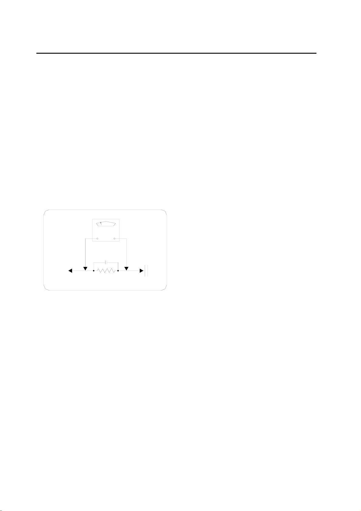
Electric leakage inspection
To device with
exposed metal parts
AC voltmeter
0.15
uF
1.5KΩ 10W
Cold water pipe
(connecting to
ground)
to protect static electricity from accumulation and explosion.
3.Solder or disassemble ES device through iron connecting
the earth.
4. Utilize device only anti-static electricity to disassemble
soldering tin. Non-anti static electricity device (ESC
protection) will release ES that damage ES device.
5.Do not use chemical volatile releasing static electricity
that leads to damage ES device
Picture1
High zeta potential leakage inspection
.As illustrated 1, Connect Resistor with 1.5K, 10W and
capacitor 0.15 between exposed metallic part and device of
fine connection to the earth (water pipe etc.).
2.Plug-in AC cord directly to AC outlet. Do not inspect with
shield adaptor.
3.Utilize 1000 or more sensitive voltmeter to measure
alternating voltage.
4.Turn back the AC plug-in from AC outlet then iterate the
inspection as above.
5.Inspect the voltage of the resistor between other exposed
metallic parts and the earth with the same way.
6. The voltage must not be over than 0.75Vrms at any points
on the resistor. Electric leakage should not be over 0.5mA
when processing high voltage leakage testing through
prevent ed static of keenness(ES)setting is exposedto static
6. Unless preparation for pre-assembling has been made,do
not take out the ES device to be changed from the protective
packings( most of the changed ES devices are packed
together with anti-static electrical foam or similar electric
material, besides, countermeasures for down-lead short
circuit are taken.).
7. Protective material should connect the model or the circuit
component to be assembled in it before taking out the
protective material from the ES device.
Note: do not bear electricity to the model or the circuit, and
pay attention to all the other safety information.
8. When disassembling and replacing the ES device, try to
reduce body movement (Or, the movement of legs, the
friction of fibrous of clothes, or elevating the legs from the
floor will generate static electricity ESD, causing damage to
the ES device.)
3
Page 5

Electric Specification
MW electric index Model No.: DVP-0601-1
Test condition:
1. Supply voltage: AC230V 50Hz 2. Standard power output: 1W
3.Speaker impedance: 4Ω(FL、FR、SL、SR),8Ω(C),6Ω(SW)
4.Standard modulating: 400Hz 30%
No.
1 Intermediate frequency KHz 450 +/-3
2 Cover with area KHz 522-1620 +/-5
4 Utility delicacy
5 S/N ratio(999 KHz,input 5mV/M) dB 40 30
6 Intermediate Frequency restrain rate(612KHz) dB 45 35
7 Mirror restrain rate(1404KHz) dB 35 30
8 Auto plus control(input 100mV/M) dB 30 20
Distortion
9
degree
10 -6dB bandwidth(20dB S/N) KHz 8 5-10
11 zip (input 5mV/M,IFx1 IFx2) % 3 10
Output
12
power
13 +/-10KHz selectivity (1000KHz 20dB S/N) dB 14 8
14 Frequency respond (-6 dB,input 5mV/M) Hz 40~4K 100~3.15K
15 Modulating AC volume (input 100mV/M) dB 40 35
16 The least noise mV 1 3
17 Sensitivity of station locking dB ≤90
5mV/M input,30% % 1 3
100mV/M input,80% % 3 5
Vol ume max W
Distortion degree: 10%,60% modulation
degree,input 5mV/M
Test items
S/N 20dB,612KHz uV/M 600 3000
S/N 20dB,999KHz uV/M 600 3000
S/N 20dB,1395KHz uV/M 600 3000
4
Unit Standard Limit error
W 4.5 3
Page 6

FM electric index Model No.: DVP-0601-1
Test condition:
1. Supply voltage: AC230V 50Hz 2. Standard output power: 1W
3. Antenna impedance: 75Ω 4. Standard modulating: 1KHz 22.5KHz
5. Speaker impedance: 4Ω(FL、FR、SL、SR),8Ω(C),6Ω(SW)
No.
1 Intermediate frequency MHz 10.7 +/-0.1
2 Cover with area MHz 87.5-108 +/-0.1
3 Utility delicacy
4 S/N ratio (98MHz,input 1mV) dB 50 34
5 -3dB limit delicacy uV 10 20
6 Intermediate Frequency Restrain Rate(90MHz) dB 50 45
7 Mirror Restrain Rate(106MHz) dB 28 22
8 Distortion degree (1mV input) % 0.6 1.5
9 Modulating AC volume(input 5mV) dB 50 40
10 Auto frequency control range(1mV input,-3dB) KHz
11 AM restrain(1mv input,modulate degree 30%) dB 32 26
Power output(distortion degree 10%,60KHz,1mv input)
12
13 Frequency response(-3dB) Hz 40~12.5K 100~8K
14 Noise of minimum volume mV 1 3
15 Sensitivity of station locking dB ≤35
16 Passage separating dB 25 ≥20
Test items Unit Standard Limit Error
S/N 30dB,90MHz dB 22 26
S/N 30dB,98MHz dB 22 26
S/N 30dB,106MHz dB 22 26
W 10
5
Page 7

DVD electric index Model No.: DVP-0601-1
1:Video section
No. Test item Test point Performance require Unit Remark
1
outp
2 S-Video
3
4
5
ut
rang
e
Y、Cr、Cb/Y、Pr、Pb
R、G、B
Horizontal distinguish
Video
Y
Chroma
C
Color
synchronization
6 Bandwidth (+3/-6dB)
7 Differential phase DP
Lum Non-Linear Distortion
8
≤5 %
9 Differential Gain DG
10
11
C
SNR
Y ≥56
U passage ≥50
V passage ≥50
R R passage ≥50
12
G G passage ≥50
B B passage ≥50
2:Audio section (testing signals:TCD-784)
No. Test item
Audio output level
1
Amplitude/Frequency response
2
Test point Performance require
1.8+0.2/-0.8 Vrms DVD(LPCM)、CD
3 S/N ratio
4
Distortion THD
5 Dynamic range
0.02 %
6 Separate degree
Passage imbalance
7
Coaxial output range
8
Optical output wavelength (λp)
9
0.5±20%
660±30
3:Other characteristics
No. Test it em Test point
Performance require
1 Disc reading time
Remote control distance
2
Supply voltage input
3
Consume power
4
Storing temperature -20℃~+55℃
5
Image signal system NTSC/PAL
6
7
Free falling
Disc format
8
230V(-10%/+10%)
Suitable for request of GB/T2423.8-1995
1)DVD Player: 12cm single face,single layer;12cm single face,double layer;8cm single face ,single
layer;8cm single face,double layer;(2)CD disc:12cm disc,8cm disc.
1.0±0.2
0.7±0.14
0.88±0.176
0.3±0.06
0.7+/-0.14
0.7+/-0.14
≥500 Line
≥5.5
≤2
≤2
±2
≥85
90
65
≤1.5
10~20
≥5
110
Vp-p
Vp-p
Vp-p
Vp-p
Vp-p
Vp-p
MHz
degree
100KHz 0dB
75Ω load
75Ω load
%
dB
dB
dB
dB
dB
dB
75Ω load
75Ω load
75Ω load
75Ω load
75Ω load
75Ω load
75Ω load
Unit Remark
dB
dB
DVD(LPCM)20Hz~20KHz
JIS-A (20KHz LPF)
1KHz JIS-A
dB
dB
dB
Vp-p
nm
1KHz JIS-A
1KHz JIS-A
DVD(LPCM)、CD
75Ω±1% load
Unit Remark
S
m
W
Normal working
50Hz
4:Test condition
1. Environment condition: normal temperature, normal voltage.
2. Supply voltage:AC230V 50Hz。
6
Page 8

Amplifier board electric index Model No.:DVP-0601-1
No. Test item Unit Typical Limit Test condition
Power supply
1 Voltage input VAC 230±10%
2 Rated output voltage & current +5V 1.3A +5V 1.5A
+12V 150mA +12V 200mA
-12V 50mA -12V 100mA
+22V 3.5A +25V 3.5A
~3.7V 100mA ~3.7V 120mA
-24V 50mA -24V 50mA
3 Output power W 110 Voltage input AC230±10%V
4 +5 wavelength output mV <50
4 Power modulating (+5V point) % 5 Voltage input AC230±10%V
6 Load modulating (+5V point) % 5 Current 10mA-1.5A
7 Standby power W ≤10
Amplifier section
1 Working voltage V +22 +26 Rated load
2 Static current mA 180 300
3 Rated load (FR/FL/SR/SL)
4 Rated load (C/SW)
Rated output power (FR/FL/SR/SL)
5
Maximum output power
6
(FR/FL/SR/SL)
7 Rated output power (C) W 15
8 Maximum output power (C) W ≧20 ≧25
9 Rated output power (SW) W 25
10 Maximum output power (SW) W ≧30 ≧35
Band distortion (FR/FL/SR/SL/C)
11
12 Band distortion (SW) % 0.25 Rated load; PO=1W;f=100Hz
13 Channel output mix dB 55
14 Channel output mix dB 55
15 S/N dB >75 JIS-A
Amplitude/Frequency response L/R/C/SL/SR
16
Amplitude/Frequency response SW
17
1 Circuit level output V
2 Circuit S/N rate output dB 90 85
3 Circuit level input V
4 Circuit impedance input Ω 10K±10%
Ω
Ω
W 12.5
W ≧16 ≧18
% 0.25 Rated load; PO=1W;f=1KHz
dB +/-2 +/-3 50Hz~20KHz
dB +/-2 +/-3 20Hz~200Hz
Audio input, output
1.5±20%
RMS
1.5±0.5
RMS
4
8
THD=10% RL=4Ω
Maximum volume RL=4Ω
THD=10% RL=8Ω
Maximum volume RL=8Ω
THD=10% RL=6Ω
Maximum volume RL=6Ω
f=1KHz
f=10KHz
Test condition
1. Test condition:Normal temperature,Normal voltage
2. Supply voltage:AC230V 50Hz。
7
Page 9

Mechanical diagram
44
44
36
44
38
37
19
45
44
24
22
48
32
48
28
42
3
8
7
9
10
13
11
15
16
4
23
22
25
3
4
31
42
5
14
6
17
45
43
20
43
47
35
43
42
1
42
12
39
41
34
40
26
45
23
25
2
18
47
44
44
46
45
24
30
44
29
21
46
21
45
43
43
43
47
46
21
46
27
45
47
21
45
47
33
8
Page 10

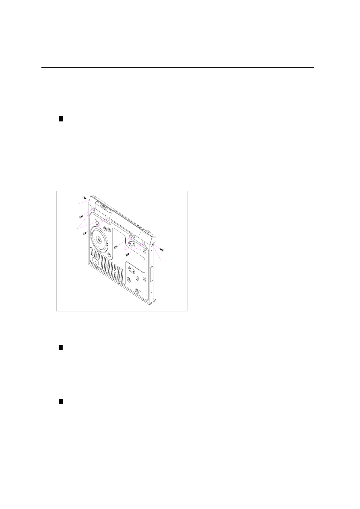
Mechanical
parts list
Material No.
No.
Name
Panel(with card reader)
decoration board
Power button
Volume button
Function button(up)
Function button(down)
Lens
Lens-A
Lens-B
Lens-C
Lens-D
Lens-E
Lens-F
Lens-G
Lens-H
Lens-I
Mother board
Back board
Top cover
Top cover holder
PCB holder(hight 7.0mm)
PCB holder(height 11.0mm)
Front feet
Rear feet
Front feet mat
Rear feet mat
Pick up CMS-S71SG6
Power switch PS4E-A-040
Decoder board
Amplifier board
Control board
Card reader board
ALPS tuner TFCF1E800A
Transformer 230V/110W/VDE
bolt H6.0×38.0mm
nut M6×4.8mm
mat φ6.0×13×1.0mm
Spring mat φ6.0×2.0mm
Fix piece for transformer φ65×6.5×1.2mm
rubber mat φ65× 7.0×1.3mm
rubber mat φ80× 7.0×1.3mm
Screw ST3X6KTT
Screw ST3X8PA
Screw ST3×6PWTT
Screw ST3×8PWTT
Screw ST3×12PWTT
Screw ST3×6PTT
Screw ST3×16PTT
Nickel
Nickel
Nickel
Nickel
Nickel
Nickel
Nickel
QTY
Remark
2
Pannel/Mother board
unit feet、loader/mother board
Amplifier board, decoder board/mother board
Mother board/rear board,tuner
Card reader board/mother board
9
Page 11

Packing and accessories
1.Disassemble
1
2
6
2.Material list
No.
1
2
3
4
5
6
Material No.
A1-060120-11
O7-060120-L0
O7-060120-R1
O7-060160-S2
A3-060120-01
O6-060127-12
4
4
Name
Remote control
Poly foam(left)
Poly foam(right)
Speaker poly foam
SPP-0301-0 type speaker
Gift box (unit+speaker)
QTY
1
1
1
2
1
1
3
5
10
Page 12
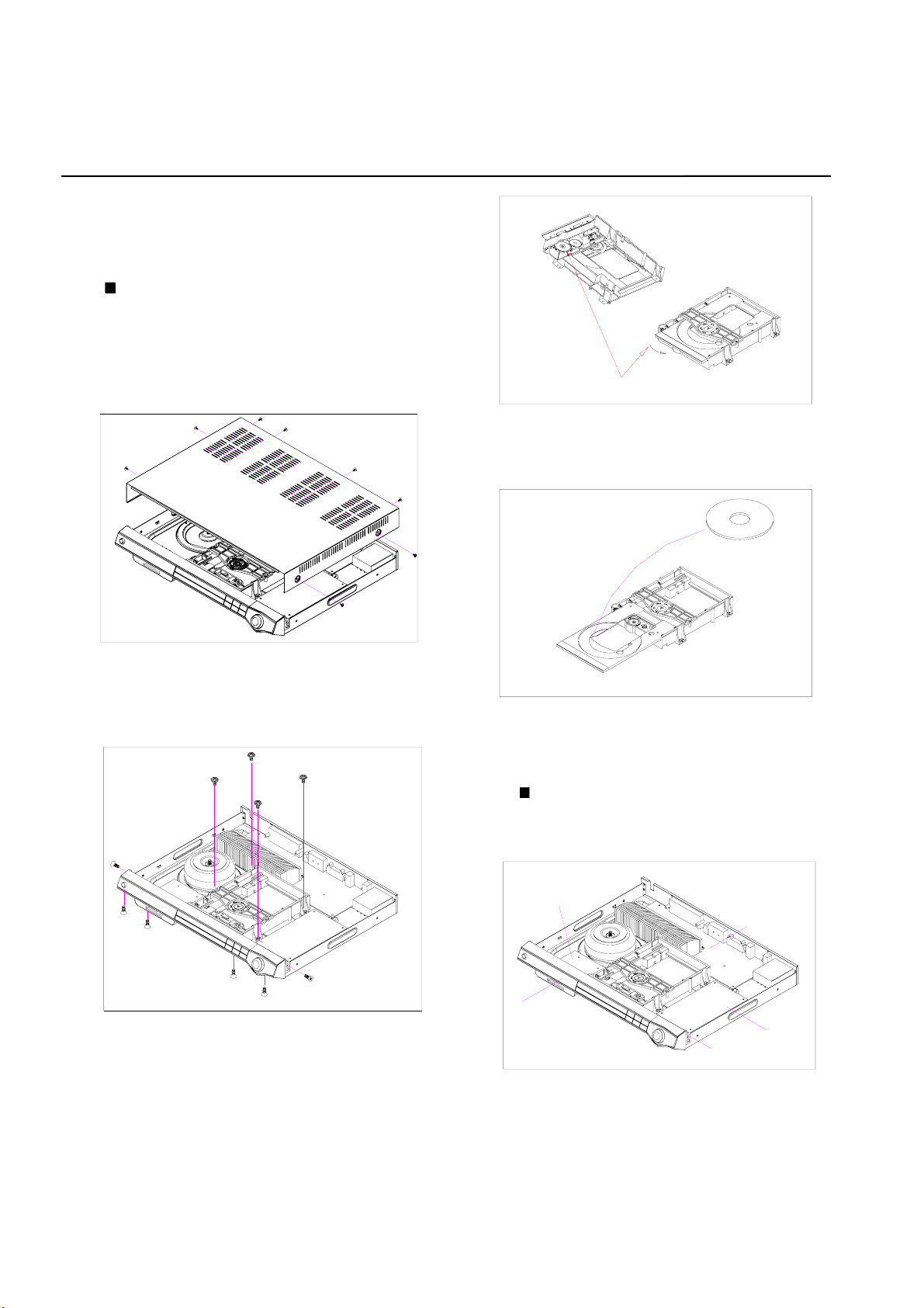
Disassemble and assemble
The unit comprises mechanical and electric part
including:front panel, base panel, top panel,
back panel and loader, AV output board,decoder,etc.
Take out disc from trouble player
If you can not take out disc even press OPEN/CLOSE
key,please pull power cord from the socket and follow
as below:1. Wring 8 screws out then pull left and
right side to take away top panel that rear part is
upper(illustrated
A)
Gear
Graph C Rotate white gear
2.Wring 6 screws out connected base panel with bottom
board then wrest 4 screws connected loader with bottom
board (illustrated B)
Graph A Dispart cabinet
Graph D Take out disc
PCB position
All PCB assemblies locate as illustrated H
card reader board
AV output board
front control board
Graph B Dispart front panel and loader
decoder board
Volume zeta board
3.Take out front panel and loader carefully, there is one
white plastic gear under the loader.Rotate the gear as
illustrated C to stretch DVD tray and door (illustrated D),
you may take disc out carefully.
Graph H PCB boards location
11
Page 13
Disassemble and assemble parts list
1.Take out top panel
See as illustrated A
2.Take out front panel
Able to open the disc tray by electricity
2.1 Operate after completely take out top panel
2.2 Press OPEN/CLOSE button to open disc tray
Be careful not to damage disc when take it out if it is in the tray.
2.3 Press OPEN/CLOSE button to close tray then pull
out power plug.
Take out PCB board on front panel and cords connected with
2.4
other circuit board.Wring out 5 screws connected front panel and
bottom panel,untie two catches on left and right side of the panel
then take out front panel.(See illustrated E)
catch
catch
catch
catch
Graph E Location of catch on front panel
Unable to open the disc tray by electricity
Unable to open disc tray when press OPEN/CLOSE button
2.1 Take out disc as illustrated A,B,C,D.
2.2 Take out front panel
Assemble the case
Assemble the case by reversing disassembly.
After maintenance,switching on power on the condition
that assembly and connection have no mistake then loader
and electric circuit return to original place automatically.
The unit works normally.
12
Page 14

Attachment 1: Block diagram, circuit diagram
Block diagram/ Connecting diagram
Decoder board diagram
Amplifier board diagram
Control board diagram
13
Page 15

Analogue audio 5.1ch
output
Digital audio output &
input (Coaxial, Optical)
Video/YUV/RGB output
SCART output
Stereo analogue audio
input/output
audio DAC-WM8772
Loader
MT1389FE
decoder, servo
Analogue amplifier
ALPS
Digital tuning FM/AM
Control board +VFD
display
+23--+27
+5V
+12V
-12V
+5V
+3V
-3V
-24V
230V
input
TRANSF.
Linear power
USB card reader
Remote control
Block diagram
14
Page 16

~230V/50HZ
SW+
SW-
AC17.5
AC17.5
AC11
ANNULAR
TRANSFORMER
P
O
W
E
R
S
W
SL
GND GND
GND
AC8.4
AC11
AC8.4
SR
RL
FR
CENT+
GND CENT- Cr
GND
Cb
COAXTAL
ML
Y
MR
SCART
VIDEO
S-VIDEO
COAXTAL
IN
POWER AMPLIFER
GND
5V
GND
AC4.5
AC4.5
AC20.8
AC20.8
GND
-3.5V
-24V
+5V
GND
+3.5V
5V
见龙机架+CMS-S71SG6
1
F-
+5V
GND
GND
-3.5V
+3.5V
-24V
O
A
F
O
R
I
F+
T+
T-
C
GND
F
A
B
D
1
I
O
1
2
D
D
O
O
M
L
I
I
NC
E
VCC
V20
VCC
G/Y
STB
B/U
GND
GND
GND
GND
R/V
-9V
+9V
2
O
D
L
NC
GND
GND
GND
GND
CVBS
GNDSYGND
SC
SR
GND
16:9
GND
CENT
LEF
RGB-C
SLED1
SLED2
SPI+
SPI+5V
GND
MLD1
MLD2
CL SW
GND
OP SW
SL
PANEL CONTROL
AUXINL
GND
DET
VSM
R
+9V
L
GND
D
O
C
L
D
I
C
E
3.3
V
RXD
TXD
GND
AM ANTENNA IN
FM ANTENNA IN
FM/AMRECEIVER
S
M
/
C
M
M
/
M
S
/
D
S
CARD
I
I
/
I
F
C
OPTICAL
IN
AUXINR
A
D
T
O
N
P
C
G
5V
GND
5V
GND
+9V
OPT
GND
COA
F
R
I
E
R
X
D
-
T
U
P
M
U
ML
GND
AUXL
GND
A
DM-L
D
S
M
MR
-9V
GND
STB
R/V
GND
B/U
GND
G/Y
GND
CVBS
GND
SY
GND
SC
RGB-C
16:9
GND
GND
LEF
GND
CENT
GND
SR
GND
SL
GND
MR
GND
ML
DM-L
MUTE
DM-R
SPDIF
AUXL
AUXR
SLED1
SLED2
SPI+
SPI+5V
GND
Progressive Scan Decoder
MLD1
MLD2
CL SW
GND
GND
DOUT
CLK
STB
IR
DIN
OP SW
O
D
X
DOUT
CLK
GND
T
GND
DIN
STB
IR
GND
E
T
VSM
RD
+9V
L
GND
D
O
C
L
D
I
C
E
FF+
TT+
C
D
IOA
RFO
A
B
F
GND
V20
VCC
E
NC
IO1
IO2
LDO
1
MDI
1
VCC
NC
LDO
2
GND
V
3
.
3
RXD
Connecting diagram
15
Page 17

Decoder board diagram(1)
16
Page 18

17
Decoder board diagram(2)
Page 19

Decoder board diagram(3)
18
Page 20

Decoder board diagram(4)
19
Page 21

Decoder board diagram(5)
20
Page 22

Amplifier board diagram(1)
21
Page 23

Amplifier board diagram(2)
22
Page 24

Amplifier board diagram(3)
23
Page 25

Control board diagram
24
Page 26

Attachment 2:PCB diagram
Upper decoder board PCB diagram
Upper decoder board silk screen diagram
Lower decoder board PCB diagram
Amplifier board PCB diagram
Amplifier board silk screen diagram
Upper control board PCB diagram
Lower control board PCB diagram
Control board silk screen diagram
25
Page 27

Upper decoder board PCB diagram
26
Page 28

Upper decoder board silk screen diagram
27
Page 29

Lower decoder board PCB diagram
28
Page 30

Amplifier board PCB diagram
29
Page 31

Amplifier board silk screen diagram
30
Page 32

Upper control board PCB diagram
31
Page 33

Low control board PCB diagram
32
Page 34

Control board silk screen diagram
33
Page 35

Attachment 3:Component list
Decoder board component list
Amplifier board component list
Control board component list
34
Page 36

Component list
Decoder board component list
No. Material No. Name Encase No. QTY
1
2
3
4
5
6
7
8
9
10
11
12
13
14
15
16
17
18
19
20
21
22
23
24
25
26
27
28
29
30
31
32
33
34
35
36
37
38
39
40
D2-010420-12 Decoder PCB board 94V0 1
C1-200500-JA 0603 capacitor 20p±5% 50V C4 1
C1-330500-JA 0603 capacitor 33p±5% 50V C10-11、125、127 4
C1-101500-JA 0603 capacitor 101±5% 50V C22、93、95、97 4
C1-151500-JA 0603 capacitor 151±5% 50V C41-42 2
C1-221500-JA 0603 capacitor 221±5% 50V C59、61、63、65、67、 8
C69、119、122
C1-331500-JA 0603 capacitor 331±5% 50V C37-38,C113 3
C1-391500-JA 0603 capacitor 391±5% 50V C1 1
C1-102500-KA 0603 capacitor 102±10% 50V C6 1
C1-152500-KA 0603 capacitor 152±10% 50V C35 1
C1-202500-KA 0603 capacitor 202±10% 50V C60、62、64、66、68、 8
C72、120、124
C1-222500-KA 0603 capacitor 222±10% 50V C3、74 2
C1-472500-KA 0603 capacitor 472±10% 50V C108 1
C1-153500-KA 0603 capacitor 153±10% 50V C40 1
C1-333500-KA 0603 capacitor 333±10% 50V C14 1
C1-473500-KA 0603 capacitor 473±10% 50V C17-18 2
C1-104500-MA 0603 capacitor 104±20% 50V
CB59-62、67、71-98、
CB101-102、
C7-9、12-13、21、
C29-30、33-34、36、39、
C43-47、92、121、123
C1-474500-MA 0603 capacitor 474±20% 50V C19、110-111 3
C1-105500-MA 0603 capacitor 1u±20% 50V C15-16、23-27 7
C2-106160-M9 Electrolyte capacitor 10u±20% 16V CE1、11、15、40、 25
CE43-44、46、48-49、
CE51、53-57、59-61、
C101-103、105、109、
C126、128、
C2-476160-M0 Electrolyte capacitor 47u±20% 16V CE16-18、21-22、28、42、 12
CE64-66、
C106-107
C2-107160-M0 Electrolyte capacitor 100u±20% 16V CE7、9、20、24、58、 8
C98-99、112
C2-227160-M0 Electrolyte capacitor 220u±20% 16V CE2、4-6、8、12-14、19、 10
CE26
C2-337160-M0 Electrolyte capacitor 330u±20% 16V CE23 1
R1-4S7103-J1 Carbon resistor 4.7Ω±5% 3w R168 1
CB1-7、10、12-36、41-50、
98
35
Page 37

Component list
Decoder board component list
No. Material No. Name Encase No. QTY
1
2
3
4
5
6
7
8
9
10
11
12
13
14
15
16
17
18
19
20
21
22
23
24
25
26
27
28
29
30
31
32
33
34
35
36
37
38
39
40
R4-1S0008-J4 0805 resistor 1Ω±5% 1/8w R42-45 4
R4-100008-J4 0805 resistor 10Ω±5% 1/8w R170-171 2
R4-0S0010-J3 0603 resistor 0Ω±5% 1/10w R9、11、21、26-30、212 11
R61-62
R4-1S0010-J3 0603 resistor 1Ω±5% 1/10w R22 1
R4-4S7010-J3 0603 resistor 4.7Ω±5% 1/10w R120、126、181 3
R4-100010-J3 0603 resistor 10Ω±5% 1/10w R24、39、41、L48 4
R4-330010-J3 0603 resistor 33Ω±5% 1/10w R63-66、77-79、105、191,192,194 22
R138-139、142-145、217、
R222-224、L23
R4-750010-F3 0603 resistor 75Ω±1% 1/10w R31、73、75、81、84、 8
R91、94、100
R4-221010-J3 0603 resistor 220Ω±5% 1/10w R57、60、97、99 4
RC-357S0A-F3 0603 resistor 357Ω±1% 1/10w R5 1
R4-561010-F3 0603 resistor 560Ω±1% 1/10w R25 1
RC-681S0A-F3 0603 resistor 681Ω±1% 1/10w R6、98 2
R4-102010-J3 0603 resistor 1KΩ±5% 1/10w R13、48、68-69、173-174、 7
R200
R4-122010-J3 0603 resistor 1.2KΩ±5% 1/10w R187 1
R4-222010-J3 0603 resistor 2.2KΩ±5% 1/10w R101、103、107、208 4
R4-472010-J3 0603 resistor 4.7KΩ±5% 1/10w R106、133、169、186、 5
R201
R4-512010-J3 0603 resistor 5.1KΩ±5% 1/10w R116、128、136、148、 8
R154、164、220、226
R4-103010-J3 0603 resistor 10KΩ±5% 1/10w R1-2、33-34、50、52、 27
R54-55、58、67、70、115、
R127、135、147、153、
R163、182-185、219、225、
R239-242
R4-153010-J3 0603 resistor 15KΩ±5% 1/10w R14、49、110、123、132、 10
R146、152、158、218、
R221
R4-183010-J3 0603 resistor 18KΩ±5% 1/10w R47 1
R4-203010-J3 0603 resistor 20KΩ±5% 1/10w R46、51、53、56 4
R4-104010-J3 0603 resistor 100KΩ±5% 1/10w R7、16、32、35、59、102,245 7
R4-154010-J3 0603 resistor 150KΩ±1% 1/10w R17、19 2
R4-684010-J3 0603 resistor 680KΩ±5% 1/10w R10、15 2
R4-754010-J3 0603 resistor 750KΩ±5% 1/10w R3 1
R6-33004J-30 0603 resistor 4×33Ω±5% RN1-2 2
L4-016008-60 0603 magnetism bead 100MHz 600 L6、17、19、26-27、 9
36
Page 38

Component list
Decoder board component list
No. Material No. Name Encase No. QTY
1
2
3
4
5
6
7
8
9
10
11
12
13
14
15
16
17
18
19
20
21
22
23
24
25
26
27
28
29
30
31
32
33
34
35
36
37
38
39
40
L30、43、47、49
L4-020012-60 0805 magnetism bead 100MHz 600Ω L1-2、7-9、11、20、 12
L24、38、L44-46
L1-100001-J0 Inductance 10uH ±5% L4-5 2
V1-141480-10 Diode 1N4148 D3-15 13
V1-5S1002-20 Zener 5.1V 1/2W D23-25 3
V1-6S8002-20 Zener 6.8V 1/2W D22 1
Z1-27S006-00 Basic oscillator 27MHz 49S type Y1 1
VC-230180-60 MOSFET 2SK3018 SC-70 Q2-3 2
VB-211320-10 Transistor 2SB1132R SOT89 Q4-5 2
VB-239040-10 Transistor SST3904/2N3904 SOT23 Q1、14-15、20 4
VB-239060-10 Transistor SST3906/2N3906 SOT23 Q16 1
V2-855000-10 Transistor 8550 TO-92 Q6-7、17 3
V2-805000-10 Transistor 8050 TO-92 Q8-9 2
IC-111700-21 IC AS1117M3/AK174J SOT223 U1 1
IC-111733-20 IC B1117N-33M142 SOT223 U2 1
IC-111700-20 IC AS1117M(3.3V) SOT223 U2
IC-138900-22 IC MT1389EE LQFP256 U4 1
IC-595400-20 IC BA5954FP HSOP-28 U5 1
IC-565400-20 IC AT5654 HSOP-28 U5
IC-126416-20 IC M12L64164A-7T TSOP54 U9 1
IC-264160-27 SDRAM N2SV6416DT-7K TSOP54 U9
IC-291607-20 IC 29LV160BE-70PFTN TSOP-48 U11 1
IC-291609-29 IC MX29LV160BTC-90 TSOP-48 U11
IC-241600-20 IC AT24C16 SO8NB U12 1
IC-455800-20 IC JRC4558 SO8NB U13、15、20、23-24 5
IC-877200-20 IC WM8772 TSSOP28 U14 1
IC-841500-20 IC CS8415A TSSOP28 U16 1
IC-744052-20 IC 74HC4052 SO16NB U18 1
IC-174200-20 IC PCM1742 SSOP-16 U22 1
IC-780900-10 IC LM7809 TO-220 Q11 1
X4-020003-10 Pin jack 3PIN/2.0mm 1800 J9 1
X4-020004-10 Pin jack 4PIN/2.0mm 1800 J8 1
X4-020005-10 Pin jack 5PIN/2.0mm 1800 J4 1
X4-020006-10 Pin jack 6PIN/2.0mm 1800 J1、7 2
X4-012511-10 Connector 11PIN/1.25mm 1800 J6 1
X4-005024-40 Pin jack 24PIN/0.5mm 900 J2 1
X3-254402-30 Pin jack 40PIN/2.54mm 1800 J10 1
37
Page 39

Component list
Amplifier board component list
No. Material No. Name Encase No. QTY
D1-060120-22 Amplifier PCB board
1
Y3-06016C-12 Heat sink holder Big heat sink 2
2
N8-182032-00 Big heat sink U4-5 1
3
N8-046017-03 Small heat sink U2 1
4
N5-049010-10 Soldering terminal X12 1
5
RA-S10002-J0 Carbon resistor 0.1Ω±5% 1/2w R2 1
6
RA-S22008-J1 Carbon resistor 0.22Ω±5% 1/8w R40-41 2
7
R1-100008-J2 Carbon resistor 10Ω±5% 1/8w R1、74 2
8
R1-330008-J1 Carbon resistor 33Ω±5% 1/8w R18、67 2
9
R1-101008-J2 Carbon resistor 100Ω±5% 1/8w R38、50 2
10
R1-121008-J2 Carbon resistor 120Ω±5% 1/8w R8 1
11
R1-151008-J2 Carbon resistor 150Ω±5% 1/8w R21 1
12
R1-221008-J2 Carbon resistor 220Ω±5% 1/8w R20、43 2
13
R1-361008-J2 Carbon resistor 360Ω±5% 1/8w R9 1
14
R1-102008-J2 Carbon resistor 1KΩ±5% 1/8w R6、48-49、68 4
15
R1-222008-J2 Carbon resistor 2.2KΩ±5% 1/8w R45-46 2
16
R1-332008-J2 Carbon resistor 3.3KΩ±5% 1/8w R16、30、69 3
17
R1-472008-J2 Carbon resistor 4.7KΩ±5% 1/8w R7、65 2
18
R1-622008-J2 Carbon resistor 6.2KΩ±5% 1/8w R19、23 2
19
R1-103008-J2 Carbon resistor 10KΩ±5% 1/8w R3、25、33-34、47、59、 10
20
R62-64、66
21
R1-153008-J2 Carbon resistor 15KΩ±5% 1/8w R35-37、39、60-61 6
22
R1-104008-J2 Carbon resistor 100KΩ±5% 1/8w R42 1
23
R1-4S7004-J2 Carbon resistor 4.7Ω±5% 1/4w R5、14-15、31、44、70-72 8
24
C1-560500-M2 Ceramic capacitor 56p±20% 50V C32
25
C1-104500-M2 Ceramic capacitor 104±20% 50V C4、26、30、33-34、40、 11
26
76-78、87、89
27
C4-104101-K3 Terylene capacitor 104±10% 50V C10、19、21、23-25、 8
28
C36-37
29
C2-474500-M9 Electrolyte capacitor 50V 0.47±20% C15-17、45-47
30
C2-105500-M9 Electrolyte capacitor 50V 1u±20% C12、49-50 3
31
C2-226350-M0 Electrolyte capacitor 35V 22u±20% C22、28 2
32
C2-476160-M0 Electrolyte capacitor 16V 47u±20% C27 1
33
C2-476350-M0 Electrolyte capacitor 35V 47u±20% C2 1
34
C2-107160-M0 Electrolyte capacitor 16V 100u±20% C90 1
35
C2-227250-M0 Electrolyte capacitor 25V 220u±20% C18、20、88 3
36
C2-337160-M0 Electrolyte capacitor 16V 330u±20% C14 1
37
C2-477250-M0 Electrolyte capacitor 25V 470u±20% C3 1
38
39
40
C2-108160-Z0
C2-108250-Z0
Electrolyte capacitor 16V 1000u+80/-20%
Electrolyte capacitor 25V 1000u+80/-20%
1
C86 1
C1、9、29、31、79 5
1
6
38
Page 40

Component list
Amplifier board component list
No. Material No. Name Encase No. QTY
C2-228100-Z0 Electrolyte capacitor 10V 2200u+80/-20% C6 1
1
C2-478160-Z9 Electrolyte capacitor 16V 4700u+80/-20% C5 1
2
C2-478350-Z9 Electrolyte capacitor 35V 4700u+80/-20% C7、8 2
3
F1-6S3011-00 Fuse T6.3AL 250V 5×20mm F1 1
4
F2-010000-00 Fuse jack F1 2
5
V1-401000-40 Bridge pile KBL401 U1 1
6
V1-140040-10 Diode 1N4004 V1-2、4-6, 5
7
C2-106160-M0 Electrolyte capacitor 16V 10u±20% C55,C59 2
8
V1-141480-10 Diode 1N4148 V8、13、 2
9
V1-560000-10 Diode SB560 D1-4 4
10
V1-5S1002-20 Zener 5.1V 1/2W V3 1
11
V1-130002-20 Zener 13V 1/2W V16 1
12
V2-273300-10 Triode A733 TO-92 V7、19-21 4
13
V2-294500-10 Triode C945 TO-92 V10-12、17-18 5
14
L4-035060-40 Magnetism bead Φ3.5×6mm100MHz60Ω L3-13、16-17、21 14
15
L1-1S8001-J0 Twist inductance 1.8uH±5% L14-15、18-20、22 6
16
L1-101001-J0 Twist inductance 100uH±5% L2 1
17
L1-101101-J0 Standing inductance 100uH±5% 2A L1 1
18
V2-781200-10 IC LM7812 TO-220 U9 1
19
IC-108400-11 ICAZ1084T-ADJ TO-220 U2 1
20
IC-894700-10 IC TDA8947J DBS17P U4-5 2
21
X1-550000-00 Optical output jack GPIFA550TZ X10 1
22
X7-284130-30 Concentric jack AV2-8.4-13A X5 1
23
Up red, Down white
24
X7-683440-30 Concentric jack AV6-8.3-44Q X11 1
25
Up white green blue, Down red yellow red
26
X1-105000-00 21 pin jack CS105 X12 1
27
X1-200000-30 S-Video + Video concentric jack SAV2 X13 1
28
X8-121000-00 Amplifier board output jack WP12-1 X9 1
29
X3-396031-31 Pin jack 3PIN/3.96 1800 X3 1
30
X4-025006-10 Pin jack 6PIN/2.54 1800 X4 1
31
X4-025009-10 Pin jack 9PIN/2.54 1800 X2 1
32
X3-254402-30 Double pin 40PIN/2.54 1800 X6 1
33
J1-0605S0-00 Jumper wire Φ0.6×5mm JMP13-14、18、25、29、 7
34
JMP39、51
35
J1-0607S0-00 Jumper wire Φ0.6×7mm JMP5 1
36
J1-0607S5-00 Jumper wire Φ0.6×7.5mm JMP8、11-12、15-17、 22
37
38
39
40
JMP20-23、26、28、30、
JMP33、36-37、40、42、
JMP43、45、48-49
39
Page 41

Component list
Amplifier board component list
No. Material No. Name Encase No. QTY
J1-060100-00 Jumper wire Φ0.6×10mm JMP3、35、41、44、46 5
1
J1-060120-00 Jumper wire Φ0.6×12.5mm JMP2、4、6、9-10、19、 14
2
JMP27、31-32、34、50、
3
JMP52-54
4
J1-060170-00 Jumper wire Φ0.6×17.5mm JMP7 1
5
J1-060200-00 Jumper wire Φ0.6×20mm JMP1 1
6
N0-300051-10 Soldering terminal X8 1
7
N2-300615-54 Screw ST3×6PWTT Nickel
8
Small heat sink and U2
9
N2-301015-54 Screw ST3×10PWTT Nickel Big heat sink and U4-5 4
10
11
12
13
14
15
16
17
18
19
20
21
22
23
24
25
26
27
28
29
30
31
32
33
34
35
36
37
38
39
40
Amplifier board, big heat sink
and holder
5
40
Page 42

Component list
Control board component list
No.
1
2
3
4
5
6
7
8
9
10
11
12
13
14
15
16
17
18
19
20
21
22
23
24
25
26
27
28
29
30
31
32
33
34
35
36
37
38
39
40
Material No. Name Encase No.
D2-060220-4K Key board
D2-060220-4V
D2-060220-40
O8-012012-20 VFD rubber mat VFD1 2
O8-070707-10 Sponge mat 7×7×7mm IC2 1
W1-351036-10 3PIN flat ribbon wires 5mm L=350mm J5-J6 1
W1-381056-10 5PIN flat ribbon wires 5mm L=380mm J7-J8 1
W3-501066-10 6PIN/2.0 flat ribbon wires L=500mm J3 1
W3-551066-20 6PIN/2.5 flat ribbon wires L=550mm J2 1
C1-104500-Z2 Ceramic capacitor 50V 104-20%+80% C1-4,C7 5
C2-107100-M0 Electrolyte capacitor 10V 100uF±20% C5,C6 2
C2-107350-M0 Electrolyte capacitor 35V 100uF±20% C8 1
R4-100016-J3 Chip resistor 1/16W 10Ω±5% R13 1
R4-330016-J3 Chip resistor 1/16W 33Ω±5% R1 1
R4-221016-J3 Chip resistor 1/16W 220Ω±5% R2 1
R4-103016-J3 Chip resistor 1/16W 10KΩ±5% R3-R4,R14-R17 6
R4-333016-J3 Chip resistor 1/16W 33KΩ±5% R9-R11,R18 4
R4-472016-J3 Chip resistor 1/16W 4.7KΩ±5% R5,R6,R8 3
R4-470016-J3 Chip resistor 1/16W 47Ω±5% R12 1
R4-563016-J3 Chip resistor 1/16W 56KΩ±5% R7 1
L4-120160-30 Magnetism annulus: K5BT16×12×8 2
V1-141480-10 Diode 1N4148 D1-2 2
V1-5S1002-20 Zener 5.1V 1/2W D3 1
V1-253021-30 LBD Φ3 red D4 1
S5-162420-00 Digital encoder EC16E-24C-20F-C S4 1
N3-090020-10 Nut M9×2mm Coding switch 1
NO-900053-10 Mat Φ9×Φ20×0.5mm Coding switch 1
Y7-010008-40 Varnished tube Φ1.0×8mm D4 2
S3-665000-00 Soft touch switch 6×6×5 S1-3 5-7 6
P3-085600-00 Display screen HNVC08SS56 VFD1 1
IC-354000-10 Receiver SRM-354VF IC2 1
IC-401300-10 IC CD4013 DIP-14 IC3 1
IC-163110-20 IC uPD16311 or CS16311 IC1 1
Decoder board
VFD board
1
1
1
QTY
41
 Loading...