

Page 1

DVD HOME THEATER SYSTEM
Model:
DVR4025VSS
SERVICE MANUAL
www.akai.ru
Page 2

1.CONTENTS
Title Page
1. CONTENTS
2. BLOCK DIAGRAM (CABLE CONNECTIONS)
3. POWER SUPPLY
4. FUNCTIONAL DESCRITPIONS
4.1 DVD MPEG board
4.2 Front Panel
4.3 SMPS
4.4 DVD Driver
5. DESCRIPTION OF THE INTEGRATED CIRCUITS
5.1 SWPS TRANSFORMER
1
2
3
4
4
10
10
12
13
13
5.2 FRONT PANEL DRIVER IC FRO VIR (PT6311)
5.3 SWPS CONTROLLER IC (5M02659)
5.4 SWPS PROGAMMABLE SHUNT RE
GULATOR (FAIRCHILD TL 431)
5.5 LINE FILTER(2 x 6.8mH)
14
18
22
23
1
1
Page 3

DVD Service Manual
2 BLOCK DIAGRAM(CABLE CONNECTIONS)
1
2
Page 4

DVD Service Manual
1
3
Page 5

DVD Service Manual
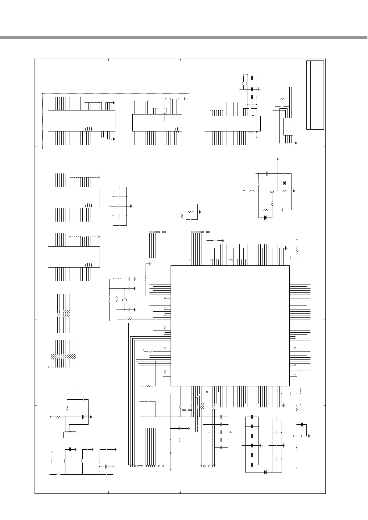
4.FUNCTIONAL DESCRIPTIONS
4.1DVD MPEG board
SEIAL
EPROM
16M
FLADH
64M
SDRAM
MT1379DE
MT1336E
AUD0
DOUT
AUD2
AUD1
AM/FM
TUNER
L/R
4053
DAC
WMA8722
CVBS
R
G
B
KARAOKE
CENTRE/SUBWOOF
SURROUND L/R
FRONT L/R
1
4
Page 6

DVD Service Manual
E
RFVCC
TROPEN
TROUT
TRCLOSE
D
C
TROPEN
L32
L33
NOT STUFF
NOT STUFF
FB 0805
FB 0805
RFVCC
RVCCIN
000
000
R143
R141
L3Ferrite Bead
B
A
+
C9
220u
CB8
0.1u
1206
C151
220u
L4Ferrite Bead
+5V DV33
+
+PS5VDV33
CB11
C6
+
1206
L1Ferrite Bead
Power Supply
CN1
SOT-223
NOT Stuffed
U1
1117-3.3
3
.1u
0
IN
G
1
220u
OUT
2
12345
TRIN
CB74
0.1u
39
10K
R146
R145
10K
CB76
0.1u
10K
R150
LIMIT
STBY
IOA
PWMOUT2
PWMOUT2
AVCC
1206
AVCC
RVCCIN
NOT Stuffed
D6
1N4001
NOT Stuffed
D7
1N4001
40
41
42
43
44
45
10K
R149
46
47
48
49
50
51
52
53
54
55
56
57
58
59
60
61
62
63
64
U2
CB94
SDATA
SDEN
SCLK
C148
URST
+
SCLK
SDATA
SDEN
URST
RVCCIN
C140
47u
+
22Ohm
R160
Q27
2SB1132
R159
22Ohm
Q26
2SB1132
+
C136
47u
CB77
0.1u
+
220u
C146
SW1
100K
15n
C135
C130
C134
R158
R156 RES
LRFRP
C129 27p
R153
0Ohm
383736353433323130292827262524232221201918171615141312111098765432
VDD
VFO13
AGNDX
AGNDX
GND
UDGATE
HDGATE
IO0
IO1
IO2
IO3
IO4
IO5
IO6
IO7
IO8
IO9
IOA
IOB
VDDS
XCK16M
SCLK
GNDS
SDEN
SDATA
RST
DPDMUTE
AGNDP
AGNDX
AVDDP
VCON
AVDDF
AGNDX
AGNDF
666768697071727374757677787980818283848586878889909192939495969798
65
CB97
0.1u
0.1u
47u
LDO1
LDO2
D5
CB2
L36
L35
CB1
D4
390p
390p
10p
C131
C133
C132
HTRC
R157 27K
DPFN
DPFO
AGNDX
HALLCOS
AVDDM
COSPHI
OP-
OPO
1N4148
0.1u
10uH
10uH
0.1u
1N4148
BDO
HTRC
BDO
RFRP
TRLP
CRTP
HTRC
GNDP
TRLPA
LRFRP
HRFRP
CRTPLP
DEFECT
AGNDM
REFCOS
HALLSIN
SINPHI
REFSIN
MOP
SW1
SW2
SW0
OP+
SW1
MDI
E
L34FB 1206
1
NC
NC
MD
HFM
LD-CD
VR-CD
LD-DVD
GND-LD
VR-DVD
CB85
33n
C16
470p
+
CB88
CB29
V2P8 V1P4
C18
RFL
CSO
TEO
RFRP
FEO
+
V2P8
V1P4
V20
FEO
RFL
CSO
TEO
LVL
V20
TM4
TEO
FEO
CSO
VDDP
AVDDT
VREFO
V2REFO
MT1336E
MON
AGNDX
AGNDX
OSP
RFFGC
OSN
RFGCU
CEON
CEOP
RFGCI
CB83
0.1u
CB84
CB82
0.1u
C139
V20
IOA
V20
10u
C138
+
10K
R148
C128
100u
+
C
D
IOA
A
B
RFO
F
F
E
A
B
D
RF
VC
VCC
CD/DVD
GND-PD
0.1u
10u
0.1u
0.1u
0.1u
10u
RFON
RFON
TM1
TM2
TM3
RFON
AGNDT
AGNDO
DVDRFIP
CDD
CDC
CDB
CDA
DVDRFIN
0.1u
C141RES
120p
RFO
R151
R147
R152
24232221201918171615141312111098765432
C
T-
F-
F+
T+
CB109
RVCCIN
0.1u
CB89
RFOP
RFOP
RFOP
DVDD
C1431uCB107
C1421u
D
A
10K
100K
100K
CB80
CB90
CON1
0.1u
CB86
1
WVDD
AGNDX
AGNDX
AVDDO
WOBSO
MT1336E
WGND
128
RFSUBO
127
LDO2
126
LDO1
125
MDI1
124
MDI2
123
AGC3
122
AGC2
121
WAVDD
120
AGC1
119
WGAND
118
SGND
117
TNI
116
TPI
115
SVDD
114
CDFON
113
CDFOP
112
SD
111
SC
110
AVDD
109
IR
108
AGND
107
SB
106
SA
105
MD
104
MC
103
DVDC
DVDB
DVDAMAMB
99
100
101
102
C1451u
C1441u
C142, C 143, C144, C145
SMD0805 Package CAP.
B
C
1Ohm
R162
1Ohm
R161
Q23
2N3904
Q24
2SK3018
Q25
2SK3018
U18BA5954FP HSOP28
1Ohm
R164
0.1u
0.1u
0.1u
SF-HD60AV/0.5mm,24Pin
1Ohm
R163
LDO2
LDO1
MDI
C147
15n
0.1u
CB79
CB78
0.1u
33K
R165
E
F
FMSO
TRSO
+PS5V
SL-
SL+
CB100.1u
171816
PGND
VOLD-
VOTK-
VOTK+
VOLD+
PGND
VOSL+
VOFC+
VOFC-
VOSL-
9
10
12
14
13
11
SP+
SP-
V1P4
STBY
C149150p
R16620K
211920
24
27
232225262930
GNDGND
BIAS
CTK2
CTK1
VINTK
VINLD
VNFTK
PVCC2
PREGND
PVCC1
CF2
CF1
VNFFC
VCC
VOSL
VINSL+
VINSL-
1
3
2157
645288
CB950.1u
R167
10K
R169 20K
R168
20K
C150150p
V1P4
DMSO
+PS5V
TO-9
Q? 8550
+5VP
TO-92
8550
Q?
47u
C153
+
CB96
0.1u
STBY
GND
RES
VINFC
C152
+
C137
10u
FOSO
12345
CN2
JST5 Pin 2.0mm Pitch
LM+
LM
-
TROUT
TRIN
220
R?
2
R?220
ADIN
OPO
750K
R170
RES
R4 10K
C139
TO-92
8050
Q?
TO-92
Q?8050
C139
RES
R5910K
R?1K
R?1K
TROPEN
TRCLOSE
OP+
OP-
R171
750K
V1P4
12345
6
CN3
R173
330K
1Ohm
R174
R172
330K
SP+
LIMIT
SL-
SL+
SP-
D
C
B
JST6 Pin 2.0mm Pitch
A
4 4
3 3
2 2
1
Page 7
DVD Service Manual
E
DV33
+PS5V
CB4
0.1u
L9FB 0805
L10RES
CB105
0.1u
FVCC
CB104
0.1u
C44
47u
+
AD0
37
29
131410
A20
VPP
VCC
WP#
DQ01
DQ00
A05
A04
A03
A02
A01
A00 RESET
WE
CE
25 12
114726
28
A3
A2
A1
PRD#
A4
PCE#
A5
PWR#
R42
+PS5V
DQ26
DQ29
DQ31
DQ30
DV33
GND
133
132
131
130
129
128
127
126
125
RD24
RD25
RD26
RD27
RD28
RD29
RD30
RD31
DVDD3
HIGHA7
AD7
AD6
AD5
AD4
DVDD3
AD3
AD2
AD1
DV33
AD0
AD2
AD1
AD5
AD3
AD4
AD7
AD6
CB18
CB17
DV33
CB15
CB14
DV33
CB13
CB5
+P5V
27
46
BYTE
GND0
GND1
OE
RY_BY
15
C2
RES
+
DV33
R4310K
10K
Q1
2N3906
R42
10K
D1
1N4148
MA2
GND
MA3
DQM0
DQM1
MA1
BA1
MA10
MA0
V25
124
123
122
121
120
119
118
117
116
115
BA1
RA3
RA2
RA1
RA0
RA10
DVSS
DQM0
DQM1
DVDD2
AD0
IOA0
IOA1
DVDD2
IOA2
IOA3
IOA4
IOA5
IOA6
IOA7
V25
A3
A4
A5
A0
A6
A7
A2
A16
A1
0.1u
0.1u
V25
0.1u
0.1u
V25
0.1u
0.1u
D12
1N4001
DQ11
DQ5
DQ13
DQ9MA9
DQ1
DQ3
DQ7
DQ8
DQ15
104611
DQ4
DQ5
A4A5A6A7A8
2930313233
MA5
DQ11DQ5
474650
DQ4
DQ5
A4A5A6A7A8
2930313233
MA5
474650
DQ4
DQ5
A4A5A6A7A8
2930313233
MA5
DQ21
R39 RES
10Ohm
Front Panel Interface
L6
4.7Ohm
DQ6
13
DQ6
MA6
MA7
DQ15
DQ13
53
DQ6
MA7
MA6
DQ1
DQ3
53
DQ6
MA6
MA7
DCS#
DRAS#
RN1 33x4
RAS#
CS#
DQ22
DQ23
R40 RES
R41 RES
JST6 Pin 2.54mm Pitch
DACV33A
FB 0805
DQ10
42
445245
DQ7
DQ8
DQ9
A9
22
343637
MA10
MA8
SD33SD33
1
DQ7
A9
22
343738
MA8
MA9
MA10
1
DQ7
A9
22
343738
10
MA
MA9
MA8
DCAS#
DWE#
WE#
CAS#
P3.1
SDA4
P3.0
R28 RES
R20 RES
R19 RES
IR
P1.5VFD_SDA
R27 33
12345
CB103
4749485051
DQ10
A10/AP
35
MA11
14
VCC
A10/AP
35
MA11
14
VCC
A10/AP
35
MA11
IOA20
R9 RES
P1.4VFD_STB
0.1u
DQ14
SD33
1
14
DQ15
CLK
SDCKE
VCCQ
CLK
SDCKE
VCCQ
CLK
SDCKE
C41
C38
+
DACV33B
CKE
62728
VSSQ
VCCQ
CKE
62728
VSSQ
VCCQ
CKE
43
3627
VCC
VCC
VCC
VSSQ
VSSQ
VSSQ
VSSQ
VCCQ
VCCQ
VCCQ
VCCQ
DQMLWECAS
RAS
CS
DCAS#
DRAS#
DCS#
VSSQ
VSSQ
VSSQ
CAS
RAS
CS
19
DCS#
DCAS#
DRAS#
VSSQ
VSSQ
VSSQ
CAS
RAS
CS
19
DCAS#
DCS#
DRAS#
100p
100u
CB102
0.1u
VSS
NC
DQMH
NC
VSS
VSS
1516171819
41
39
40
54
28
DQM0
DWE#
DQM1
41
54
VSS
VSS
VSS
DQM
WE
161718
39
DQM1
DWE#
41
54
VSS
VSS
VSS
DQM
WE
161718
39
DQM0
DWE#
DACV33C
L8
FB 0805
CB52
CB48
CB47
SD33
CB45
CE29
+
RES
(2.7uH)
R4 100K L5
R5 33Ohm
CB30
0.1u
C154
220u
+
CB27
0.1u
53
DQ11
DQ12
DQ13
DQ14
A11
BA0/A13
BA1/A12
38
20
21
BA1
SDCLK
BA0 DQ12
435249
VCC
VCC
VCCQ
A11
BA0/A13
BA1/A12VCCQ
20
21 3
SDCLK
DBA0
DBA1
435249
VCC
VCC
VCCQ
BA0/A13
BA1/A12VCCQ
A11
20
21 3
DBA0
SDCLK
DBA1
P1.5
R8 RES
P1.3VFD_SCK
6
L7
FB 0805
AD3
AD2
AD0
AD1
AD4
AD5
AD6
252627
28
3233343511
D0D1D2
D3
D4D5D6
TSOP40
OPTIONAL
U9SST39VF080
A0A1A2A3A4A5A6A7A8
21201918171615
A2
A4
A5
A0
A1
A3
0.1uF
0.1uF
0.1uF
0.1uF
47uF
C11
RES
(1nF)
R11 1K
C14
22p
Y1
27MHz
C13
22p
R175
33Ohm
R10
CB28
0.1u
C21
V2P8
URST
RFRP
HTRC
BDO
SCLK
SDEN
SDATA
V1P4
V1P4
V2P8
SDEN
SCLK
RFRP
SDATA
HTRC
DQ2
DQ0
E
D
C
B
A
DQ4
2
4125
798
DQ0
DQ1
DQ2
DQ3
A0A1A2
A3
U5 4M16/2M16 SDRAM
54-Pin TSOPII (400mil x 875mil)
232425
26
MA0
MA3
MA4
MA1
MA2
DQ14
DQ9
DQ12
DQ10
DQ8
2
5128
11944
DQ0
DQ1
DQ2
DQ3
A0A1A2
A3
U9 8M8 SDRAM
54-Pin TSOPII (400mil x 875mil)
232425
26
MA0
MA3
MA2
MA4
MA1
DQ7
DQ4
DQ6
DQ0
DQ2
2
5128
11944
DQ0
DQ1
DQ2
DQ3
A0A1A2
A3
U8 8M8 SDRAM
54-Pin TSOPII (400mil x 875mil)
232425
26
MA4
MA1
MA3
MA0
MA2
SDCKE
SDCLK
R32 33Ohm
R31 33Ohm
DCLK
DCKE
DQ18
DQ19
DQ16
DQ20
DQ17
R34 RES
R35 RES
R36 RES
R37 RES
R38 RES
+PS5V
R26
+PS5V
J5
SD33
1206
L11Ferrite Bead
R6
DV33
AD7
D7
8
14
A8
A7
18K
1000p
R7
CB110
CB87
TEO
ADIN
BDO
ADIN
TEO
2910123831
NC
NC
NC
A9
A10
A12
A11
A13
7
56432
36
A10
A9
A11
A13
A12A6A14
Y2Y3Y1Y5Y6Y4VSYNC#
Y3Y2Y1Y6Y5Y4VSYNC#
100K
RFIN
0.1u
C22 1000p
0.1u
RFON
CSO
FEO
RFL
RFON
CSO
FEO
RFL
FVCC
AD2
AD4
AD5
AD6A0AD3
DQ11
A15
RD18
DVSSFGHIGHA0
DQ10
A14
A15
1K
143
RD19
DQ09
DQ08
DQ07
A13
A12
A11
A14A6A11A7A9
A13
A12 AD7
V25
DQ22
DQ21
DQ20
142
141
140
RD20
RD21
DVDD2
HIGHA1
HIGHA2
A8
A9
A11
A10
C36
330p
C35
330p
C37
RES
C34
15n
CB35
0.1u
DQ06
A10
139
RD22
HIGHA3
DQ05
A09
8
A10
DQ23
138
137
RD23
HIGHA4
A13
A12
AD1
DQ04
DQ03
DQ02
A08
A07
A06
18192021222324
A8
GND
DQ24
136
135
134
DVSS
DQM2
DQM3
MT1379_216
HIGHA5
DVSS
HIGHA6
GND
A15
A14
V1P4
30
23
VSSWEVSS
VCC
VCC
RY/BY
RESET
A18
CE
A14
A15
A16
A17
A19
OE
9 39
1
372413
22
40
A19
A15
A17
PRD#
A16
PWR#
PCE#
A18
CB33
R16
C32
HSYNC#
HSYNC#
GND
Y1
DACV33B
Y2
GND
Y3
DACV33A
Y4
GND
Y5
Y6
VSYNC#
ADC_DAT
GND
HSYNC#
V25
DV33
GND
DV33
BDO
GND
ADIN
TEO
CSO
FEO
RFL
AV33
RFIP
C23 1000p
RFOP
RFOP
R13 RES
DACV33C
162
161
160
159
158
FS
SMD LQFP-216
163
164
165
166
167
168
169
170
171
172
173
174
175
176
177
178
179
180
181
182
183
184
185
186
187
188
189
190
191
192
193
194
195
196
197
198
199
200
201
202
203
204
205
206
207
208
209
210
211
212
213
214
215
216
ICE
TEI
FEI
R14
AV33
DACVSSC
YUV1/C
DACVDDB
YUV2/Y
DACVSSB
YUV3/CVBS
DACVDDA
YUV4/G
DACVSSA
YUV5/B
YUV6/R
BLANK#
VSYN
YUV7
DVSS
HSYN
SPMCLK
SPDATA
DVDD2
SPLRCK
SPBCK
DVDD3
XTALO
XTALI
PRST
DVSS
VFO13
IDGATE
DVDD3
UDGATE
WOBSI
SDATA
SDEN
SLCK
BDO
ADCVSS
ADIN
RFSUBI
TEZISLV
CSO
RFLEVEL
RFRP_DC
RFRP_AC
HRFZC
PWMVREF
PWM2VREF
ADCVDD3
RFDTSLVP
RFDTSLVN
RFIN
RFIP
IREF
123456789
R15 8.2K
CB22
0.1u
C24
47u
+
4.7Ohm
VREF
YUV0/CIN
DACVDDC
PLLVSS
LPIOP
LPION
LPFON
C29 10n
C28 10n
C30 10n
U5 MT1379E
454341393634323044424038353331
DQ15
DQ14
DQ13
DQ12
A19
A18
A17
A16
U118M/16M Flash
48Pin TSOP (Standard Type, 12mm x 20mm)
9
1234567
161748
A20
A17
A19
A16
A18
RES
560
RES
ASDAT2
ASDAT1
ASDAT0
ABCK
ALRCK
ASPDIF
MUTE
ADC_DAT
ACLK
R23
ABCK
ASDAT2
MUTE
ADC_DAT
ASPDIF
DV33
ASDAT0
ACLK
ASDAT1
157
156
155
ASDATA4
ASDATA3
ASDATA2
LPFIP
LPFIN
LPFOP
C31 10n
GND
ALRCK
154
153
152
151
150
149
148
147
146
145
144
RD16
RD17
ACLK
ABCK
DVSS
SPDIF
ALRCK
DVDD3
ASDATA1
ASDATA0
MC_DATA
JITFO
JITFN
PLLVDD3
FOO
TRO
TROPENPWM
PWMOUT1
PWMOUT2
DVDD2
DMO
FMO
10111213141516171819202122232425262728293031323334353637383940414243444546474849505152
V25
GND
R21 10K
R22 15K
R18 20K
R17 750K
R19 18K
C33 100p
FMSO
FOSO
DMSO
PWMOUT2
TRSO
TROPEN
PWMOUT2
DMSO
FMSO
FOSO
TRSO
TROPEN
SDA
SCL
R24
1K
R25
1K
678
SCL
VCC
RST/WP
CB510.1u
DC/NC
RST_/NC
WP/RST_
VSS SDA
123
4 5
U10 EEPROM 24C16 SOP8
URST
URST
C7
10n
D10
RES
R1
1K
R4310K
+
C5
10u
AV33
MA7
MA4
DV33
MA6
MA5
114
113
112
111
110
RA4
RA5
RA6
DVSS
DVDD3
IOA20
A16
A17
IOA18
IOA19
53
54
A17
A19
A18
A20
CB100
0.1u
CB20
0.1u
CB19
0.1u
CB9
0.1u
C10
220u
+
R304.7Ohm
C39
2.2u
0805
109
RA7
DMVSS
DMVDD3
108
RA8
107
RA9
106
RA11
105
CLE
104
CLK
103
DVSS
102
GND
RD8
101
RD9
100
RD10
99
RD11
98
DVDD3
97
DV33
RD12
96
RD13
95
RD14
94
RD15
93
DVSS
92
GND
BA0
91
RCS#
90
RAS#
89
CAS#
88
RWE#
87
RD0
86
RD1
85
RD2
84
RD3
83
DVDD2
82
V25
RD4
81
RD5
80
RD6
79
RD7
78
DVSS
77
GND
URD#
76
UWR#
75
UP3_5
74
UP3_4
73
DVDD2
72
V25
IR
71
INT0#
70
UP3_1
69
UP3_0
68
UP1_7
67
DVDD3
66
DV33
UP1_6
65
UP1_5
64
UP1_4
63
UP1_3
62
UP1_2
61
DVSS
60
GND
IOCS#
59
IOWR#
58
IOOE#
57
ALE
56
APLLVDD3
55
APLLVSS
R33 10K
C40
2.2u
0805
FVCC
R294.7Ohm
CB3 Placed
CB3
0.1u
AV33
AV33
+
C4
220u
1206
L2Ferrite Bead
DV33
of
2 4Wednesday, July 28, 2004
E
MAXITECH Technology Co., LTD.
Maxitech DVD-Receiver MT1379 Solution
Title
Size Document Number Rev
Date: Sheet
D
C
MA8
MA9
MA11
DCKE
DCLK
DQ8
DQ9
DQ10
DQ11
DQ12
DQ13
DQ14
DQ15
BA0
CS#
RAS#
CAS#
WE#
DQ0
DQ1
DQ2
DQ3
DQ4
DQ5
DQ6
DQ7
TXD
RXD
IR
P3.1
P3.0
SDA
SCL
P1.5
P1.4
B
P1.3
PCE#
PWR#
PRD#
Near Pin
212
A
The information has been checked and is believed to be reliable. However, no responsib time in order to improve the design.
4 4
3 3
2 2
1 1
1
6
Page 8

DVD Service Manual
4
FR
C35
22p
L30
FB
Q30
E
C49
R3515k
D
A+12V
C
B
A
C53
R3815k
U14WM8772/DA1172
R52 10 Ohm
R51 RES
+5V
2N3904
C34
10u
+
R178
1K
R1511K
A_MUTE
1
U10A
4558
SOP8
+
-
3
2
220pF
R37
5.1k
R36
10k
+
CE19
10uF
DAC_FR
FL FR
FL
FB
C24
10u
+
R157
1K
7
U10B
4558
SOP8
+
-
5
6
220pF
R54
5.1k
R40
10k L10
+
CE24
10uF
DAC_FL
+5VA
151617
18
28
VMID
AVDD
VFEFP
TESTREF1
SSOP28
MODE
DVDD
ML/I2S
MC/IWL
1
5
111213
+5VA
AXIAL 0.4
R196 FB
DV33
R3215k
C50
2000pF
C15
22p
Q10
2N3904
R1511K
A_MUTE
8 4
A-12V
R2915k
C54
2000pF
C55
220uF
+
DAC_FR
DAC_FL
CB106
0.1uF
CB58
0.1uF
C54
10uF
+
CB57
0.1uF
C8
10uF
+
2122232425
27
AGND
VREFN
VOUT1L
MCLK
DGND
MD/DM
MUTE
234
6
14
CB56
0.1uF
+
C53
220uF
RN2 33x4
ABCK
ACLK
ACLK
SR
C35
22p
L30
FB
Q30
2N3904
C34
10u
+
R137
1K
R1511K
A_MUTE
1
U13A
4558
SOP8
+
-
3
2
C43
220pF
R34
5.1k
C46
2000pF
R1815k
R33
10k
+
CE10
10uF
SL
C25
22p
L20
FB
Q20
2N3904
C24
10u
+
R151
1K
R1511K
A_MUTE
7
U13B
4558
SOP8
A+12V
+
-
8 4
A-12V
5
6
C32
220pF
R31
5.1k
C33
2000pF
R9 15k
R30
10k
+
CE8
10uF
DAC_SL DAC_SR
AINL
AINR
DAC_SR
DAC_LFE
DAC_CENT
DAC_SL
C133
10nF
C145
10nF
19
20
26
AINL
AINR
VOUT2L
VOUT3L
VOUT1R
VOUT2R
VOUT3R
Hardware
BCLK
LRC
789
ALRCK
ASDAT0
ALRCK
ABCK
Con
DIN1
DIN2
DIN3
DOUT
10
RN2 33x4
ASDAT1
ASDAT2
ADC_DAT
ASDAT2
ASDAT0
ASDAT1
ADC_DTA
78L05
24Bit-I
U103
CENT
C35
22p
123456789
L30
FB
Q30
2N3904
C34
10u
+
R117
1K
R1511K
1
U15A
4558
SOP8
+
-
3
2
C29
220pF
CB9
A-12V
OPAMPs U10, U13 & U15
Decoupling Capacitors
A+12V
+5VA
A-12V
D?
R191 1K
CE43
CB76
CB76
VEE
VDD
15246109
R197RES
MIC2
AUX1_R
AUX2_R
TUNER_R
0.1uF
CB8
0.1uF
CB7
0.1uF
CB6
0.1uF
CE6
47uF
16V
+
CB9
0.1uF
CB8
0.1uF
CB7
0.1uF
CB6
0.1uF
CE6
47uF
16V
+
5.1V
+
47uF
0.1uF
0.1uF
VSS
C227
RES
C226
RES
DQ30
DQ29
R26
5.1k
C31
2000pF
R24
10k
+
CE7
10uF
DAC_CENTDAC_LFE
LFE
C35
22p
L30
FB
Q30
2N3904
C34
10u
+
R129
1K
R1511K
A_MUTE A_MUTE
7
U15B
4558
SOP8
A+12V
+
-
8 4
A-12V
5
6
C19
220pF
R12
5.1k
C20
2000pF
R11
10k
+
CE5
10uF
AINL
AINR
+
4052
R82 150
R84 150
+
CE5 10uF
CE6 10uF
1331687
X
Y
SOP16
X0X1X2X3Y0Y1Y2Y3INHAB
U?
121415
11
R196RES
+
CE8 10uF+CE7 10uF
MIC1
AUX1_L
AUX2_L
TUNER_L
CE43
RES
+
CB73
RES
1
OUT
G
2
IN
TO-92 (Reserved)
3
CB73
RES
+
CE43
RES
A+12V +5VA
OPTIONAL
JP?
SLSRCENT
LFE
FR
FL
AMP_STBY
DQ16
SPDIFOUTASPDIF
R111330
R10868
C1720.1u
U13D
74HC04
U13E
9 8
11 10
U13C
5 6
U13B
3 4
U13A
1 2
R103
10M
VCC
C163
R10433
Audio Out
JST9 Pin 2.0mm Pitch
R112
91
74HC04
74HC04
74HC04
74HC04
0.1u
mm Pitch
CON8
Audio Input
JST 12Pin 2.0
RCA Jack
P2 Audio Output
+PS5V +5V +12V -12V A+5V
+3.3V
JP?
Power Supply
U13F
13 12
R1051M
1234567891011
AUX2_R
AUX2_L
MIC_DECT
FLFRSLSRCENT
123456789
JST10 Pin 2.54mm Pitch
74HC04
12
MIC2
AUX1_L
AUX1_R
RXP3
MIC1
RXP2
LFE
RSL
RSR
R138
RESD11N4148
R138
RES
A_MUTE
R106
100K
Q712N3906
R932.2k
R91
4.7K
10
MUTE
DV33
A2
2 3Friday, July 30, 2004
E
MAXITECH Technology Co., LTD.
7.1-Channel DivX DVD-Receiver
Title
Siz Document Number Rev
Date: Sheet of
D
CE5
10uF
+
C
B
A
The information has been checked and is believ ed to be reliable. However, no responsibility is assumed for inaccuracies. Circ uit diagrams are provided as a means of illustrating ty pical applications; MAXITECH Technology reserves the right to make changes at any time in order to improve the design.
4
3 3
2 2
1 1
7
Page 9

DVD Service Manual
DQ20
123456789101112131415
CON9
To Output Board
JST 15Pin 2.0mm Pitch
FL
FR
R/V
G/Y
CVBS
FL
FR
P1
S-Video+RCA
8
9
CVBSSYSCSC
L281.8uH
D13
1N4148
+P12V
Q17
8550
TO- 92
R89
B/U
HSYNC#
VSYNC#
RGB/CVBS#
16:9
SPDIF
RGB/CVBS#
+5V
HSYNC#
VSYNC#
SPDIF
7
6
CY
GG
5
1 2
3 4
C56
47pF
C55
47pF
D15
1N4148
R91
150
1%
C85
0.1u
Q71
2N3906
R106
DV33
16:9 Control Signal to TV set:
16:9
Q74
R71
1K
R74
2.2k
R70
680
4.7K
RGB_Switch
+12V
DQ20
C56
L281.8uH
C55
D13
D15
1N4148
R91
150
Y6Y5G/Y B/U R/VY4
Y6Y4 Y5
2N3904
Q70
2N3904
R722.2k
R942.2k
FS0
FS1
DQ22
DQ21
47pF
47pF
1N4148
1%
R96
680
L13
FERB
C126
0.1uF
CE1
100uF
+
TUNER VCC
U28
TUNER ON/OFF
R50
10K
Q14
2N3904
1K
CE2
47uF
+
D12
5.1V
CE4
47uF
+
RDS_VCC
CB1
0.1uF
+
CE3
2.2uF
R97
2.2K
C223
15
6
10
9
3125
T57
VSS1
TEST
VREF
VDDA
VDDD
MODE
QUAL
RDATA
RCLK
PT2579/BU1924F
SOP16
1
2
16
P3.1
DQ31
P3.0
XIN XOUT
VSS3VSS2
CMP
MPXIN
7 11
8
4
13 14
C224
560pF
C225330P
MPX
PT2579/BU1924F or
82pF
Y2 4.332MHz
C220
47pF
R81
RES
Equivalent Part.
PT2579: R81=OPEN
BU1924F: R81=0
C52
C52
47pF
L321.8uH
C51
47pF
D18
D17
V33 V33 V33
D19
1N4148
1N4148
R81
150
1%
C48
47pF
L351.8uH
C47
47pF
D20
1N4148
1N4148
R73
150
1%
Y1 SY Y2 Y3 CVBS
Y1 Y2 Y3
D17
V33 V33V33
D19
47pF
L321.8uH
C51
47pF
D18
1N4148
1N4148
R81
150
1%
VCC
C48
47pF
L351.8uH
C47
47pF
D20
1N4148
1N4148
R73
150
1%
TUNER VCC
R99
10K
RN4
10Kx4
R75
10K
R180
10K
DQ21
DQ30
DQ29
Radio-L
12345678910111213
CON7
Tuner Connector
FFC CON 13 Pin 1.27mm Pitch
C130
100p
C233
100p
C230
100p
C232
100p
C93
100p
C94
100p
C128
PLL_CLK
PLL_CE
RN2 330x4
DQ23
DQ24
DQ22
Radio-R
100p
PLL_DAT
C95
100p
R179 330
R72 330
P3.1
P3.0
MPX
P1.3
P3.1
DQ26
1
8
Page 10

DVD Service Manual
1
9
Page 11

4.2.1 Front Panel Interface
6 Pin, Data Connector Pin Assignments
PIN NAME I/O DESCRIPTION
1 DATA I IR sensor interrupt
2 CLK O Front Panel chip select
3 STB O Front Panel clock
4 GND O Front Panel Data output
5 VCC
6 REM I Front Panel Data input
3Pin, Power Connector Pin Assignments
DVD Service Manual
PIN NAME FROM DESCRIPTION
3 -21V SMPS the cathode.
PT6311 S0791GC
There are 3 different devices operated by the and (Optional):
* Vacuum Fluorescent Display (VFD)
* Push-buttons
* VFDs
There is an option for a tray lamp and a joystick which is not currently assembled. The VFD display is
custom made,
implemented in a 6 grids by 16 segment matrix.
The VFD needs special voltage supply for operation:
* Vkk which is -21V needed to drive the segments and grids of the VFD.
* Vf1, Vf2 which powers the exectron cloud filament (cathode) with a differential voltage of 3.5V. This is
a floating
voltage difference generated by the power supply, and is biased to -21V in the ront panel board by a
Zener circuit
from the -21V (Vkk) supply. Moving the bias towards a more positive number will reduce the segment
brightness.
Vf1 & Vf2 provide a DC supply to the cathode. To overcome the voltage difference between one end
and the other
of the cathode, it is geometrically titled so that the segments observe the same potential and have all
the same
brightness. Other way to overcome the problem is to employ an AC supply to power the Vf1 and Vf2.
1 VFD 1 SMPS Segment and grid Voltage of the VFD
2 VFD 2 SMPS Provide a DC supply to the cathode. To vercome
the voltage difference between one and the other of
4.3 SMPS
The mains power(220VAC) fed from K1is filtered through 3C1, 3L1, 3C2 then rectified by D1,D2, D3 and
D4 and generates an output at 300VDC. This 300VDC fed to 3TR1 (pin1, pin5) which
connects to 5M02659R(pin3), then 5M02659R will automatically generate a 50KHz square waveform,
this 50KHz square waveform controls the ON/OFF between 5M02659R pin1 and the ground.
In normal condition, T1 primary (between pin2 and pin4) will create a 50KHz square waveform
which is controlled by 5M02659R, this signal then fed to 3TR1 and generates 2 different potential
voltages of 12V and 5V .The 12VDC and 5VDC
then rectified by3D11 and then filtered by3 L2, 3R9, 3C18, 3CC25 and 3C11. The feedback voltage
is controlled by Ic3 TL431 and IC2 PC817. When the output voltage is higher than 5V, the voltage at
TL431(2.5V) is compared with R10 and send out a signal to 5M02659R, the output square waveform then
will change to adjust the output voltage, this acts as a voltage stabilizer.
10
1
Page 12

DVD Service Manual
11
1
Page 13

DVD Service Manual
12
1
Page 14

DVD Service Manual
5. DESCRIPTION OF THE INTEGRATED CIRCUITS
5.1 SMPS TRANSFORMER
1. GENERAL INFORMATION
Main Voltage Operations:
Main Drop-out Voltage:
Mains STart-up Voltage:
Operating Frequency:
90Vac - 265 Vac
Max. 90 Vac
Max. 90 Vac
60 KHz
2. ELECTRICAL CHARACTERISTICS
2.1 STATIC CHARACTERISTICS
WINDING
PrimaryInductance
PIN.NO
2-4
1. Primary Leakage inductance (Pin 2-4) L1.5mH
INDUCTANCE 6DESCRIPTION
1.5mH10% <0.50W
2.2 WITHSTANDING VOLTAGE
The transformer shall sithstanding a voltage of 4 Kvms for 1 minute and 1 mA between
primary and seconday winding and also 2 Kvms for 1 minute and 1 mA between
primary winding with core and secondary winding with core.
2.3 INSULATION RESISTANCE
The insulation resistance shall be ore than 500M between primary and seconday
windings when the applied voltage 300 Vdc for 1 minute
2.4 ELECTRICAL CHARACTERISTICS
1. Before taking measurement Pp01 will be to give 5.0Vdc on 5.0Vdc line at Minimum
setting of controls and a mains voltage 220 Vac.
2. Before taking a measurement, DVD set should be working at least 5 minutes on
Normal condition
13
1
Page 15

DVD Service Manual
5.2 FRONT PANEL DRIVER IC FOR VIR (PT6311)
5.2.1 General Description
14
1
Page 16

DVD Service Manual
15
1
Page 17

DVD Service Manual
1161
Page 18

DVD Service Manual
17
Page 19

DVD Service Manual
5.3 SWPS CONTROLLER IC ( )5M02659
18
1
Page 20

DVD Service Manual
19
1
Page 21

DVD Service Manual
20
1
Page 22

DVD Service Manual
21
1
Page 23

DVD Service Manual
22
Page 24

DVD Service Manual
23
1
 Loading...