

Page 1

Service Guide
Agilent Technologies
ESG Family Signal Generators
Serial Number Pref i xes :
(Affix Label Here)
Part No. E4400-90335
Printed in USA
August 2003
© Copyright 1999-2003 Agilent Technologies Inc.
Page 2

ii
Page 3

Contents
1. Initial Troubleshooting and RF Block Diagrams
Before You Begin Troubleshooting . . . . . . . . . . . . . . . . . . . . . . . . . . . . . . . . . . . . . . . . . . . . . .1-2
Using this Service Guide to Troubleshoot. . . . . . . . . . . . . . . . . . . . . . . . . . . . . . . . . . . . . . . . .1-2
Signal Generator Options . . . . . . . . . . . . . . . . . . . . . . . . . . . . . . . . . . . . . . . . . . . . . . . . . . . . .1-3
Contacting Agilent Technologies. . . . . . . . . . . . . . . . . . . . . . . . . . . . . . . . . . . . . . . . . . . . . . . .1-8
Check the Basics before Contacting Agilent Technologies . . . . . . . . . . . . . . . . . . . . . . . . . .1-8
Review the Warranty . . . . . . . . . . . . . . . . . . . . . . . . . . . . . . . . . . . . . . . . . . . . . . . . . . . . . . .1-8
Calling Agilent Technologies Sales and Service Offices . . . . . . . . . . . . . . . . . . . . . . . . . . . .1-8
Returning Y our Signal Generator for Service . . . . . . . . . . . . . . . . . . . . . . . . . . . . . . . . . . .1-10
Equipment Required for Troubleshooting . . . . . . . . . . . . . . . . . . . . . . . . . . . . . . . . . . . . . . .1-11
Initial Troubleshooting . . . . . . . . . . . . . . . . . . . . . . . . . . . . . . . . . . . . . . . . . . . . . . . . . . . . . .1-12
Step 1: Observe the Front and Rear Panel LEDs . . . . . . . . . . . . . . . . . . . . . . . . . . . . . . . .1-12
Step 2: Power On the Signal Generator and Check for Error Messages . . . . . . . . . . . . . .1-13
Step 3: Functional Check the Front Panel Keys and Display . . . . . . . . . . . . . . . . . . . . . .1-14
Step 4: Visually Check the Individual Voltage Supplies. . . . . . . . . . . . . . . . . . . . . . . . . . .1-15
Step 5: Measure the Individual Vo ltage Supplies. . . . . . . . . . . . . . . . . . . . . . . . . . . . . . . .1-16
Step 6: Isolate the Failed Assembly . . . . . . . . . . . . . . . . . . . . . . . . . . . . . . . . . . . . . . . . . . .1-19
Step 7: Check for Basic CPU Functionality. . . . . . . . . . . . . . . . . . . . . . . . . . . . . . . . . . . . .1-21
Additional Information for Troubleshooting the ESG-AP and ESG-DP Series . . . . . . . . . .1-23
ESG-A Series RF Block Diagram (Standard & Option 1E6) . . . . . . . . . . . . . . . . . . . . . . . . .1-25
ESG-D Series RF Block Diagram . . . . . . . . . . . . . . . . . . . . . . . . . . . . . . . . . . . . . . . . . . . . . .1-27
ESG-D Series RF Block Diagram (Options UN3 & UN4) . . . . . . . . . . . . . . . . . . . . . . . . . . .1-29
ESG-D Series RF Block Diagram (Option UN8 or UN9) Rev C or D . . . . . . . . . . . . . . . . . .1-31
. . . . . . . . . . . . . . . . . . . . . . . . . . . . . . . . . . . . . . . . . . . . . . . . . . . . . . . . . . . . . . . . . . . . . . . . . .1-32
ESG-D Series RF Block Diagram (Options UN8 & UN9) Rev B. . . . . . . . . . . . . . . . . . . . . .1-35
ESG-D Series RF Block Diagram (Option UND) . . . . . . . . . . . . . . . . . . . . . . . . . . . . . . . . . .1-37
ESG-D Series RF Block Diagram (Option UN7, UN8/UN9, & 300) . . . . . . . . . . . . . . . . . . .1-39
ESG-AP Series RF Block Diagram (Standard & Option 1E6). . . . . . . . . . . . . . . . . . . . . . . .1-41
ESG-DP Series RF Block Diagram . . . . . . . . . . . . . . . . . . . . . . . . . . . . . . . . . . . . . . . . . . . . .1-43
ESG-DP Series RF Block Diagram (Option UN7) . . . . . . . . . . . . . . . . . . . . . . . . . . . . . . . . .1-45
ESG-DP Series RF Block Diagram (Options UN8 & UN9) . . . . . . . . . . . . . . . . . . . . . . . . . .1-47
ESG-DP Series RF Block Diagram (Option UND). . . . . . . . . . . . . . . . . . . . . . . . . . . . . . . . .1-49
Blue Repair Tags . . . . . . . . . . . . . . . . . . . . . . . . . . . . . . . . . . . . . . . . . . . . . . . . . . . . . . . . . . .1-51
2. Assembly-Level Troubleshooting with Block Diagrams
Before You Begin Troubleshooting . . . . . . . . . . . . . . . . . . . . . . . . . . . . . . . . . . . . . . . . . . . . . .2-2
Using this Chapter with Service Software . . . . . . . . . . . . . . . . . . . . . . . . . . . . . . . . . . . . . . . .2-2
A5 Dual Arbitrary Waveform Generator Block Diagram (Option UND) . . . . . . . . . . . . . . . .2-5
A6 Bit Error Rate Test Block Diagram (Option UN7) . . . . . . . . . . . . . . . . . . . . . . . . . . . . . . .2-7
A7 Baseband Generator Block Diagram (Options UN3 & UN4). . . . . . . . . . . . . . . . . . . . . . .2-9
A7 DBMIC Baseband Generator Block Diagram (Options UN8 & UN9). . . . . . . . . . . . . . .2-11
A8 Data Generator Block Diagram (Options UN3 & UN4). . . . . . . . . . . . . . . . . . . . . . . . . .2-13
A8 Data Generator - Rev. A & B Block Diagram (Options UN8 & UN9) . . . . . . . . . . . . . . .2-15
A8 Flex Data Generator - Rev. C & D Block Diagram (Options UN8 & UN9) . . . . . . . . . . .2-17
A9 Output ABUS Nodes (ESG-A Series) . . . . . . . . . . . . . . . . . . . . . . . . . . . . . . . . . . . . . . . .2-19
A9 Output Block Diagram (ESG-A Series) . . . . . . . . . . . . . . . . . . . . . . . . . . . . . . . . . . . . . . .2-21
A9 Output ABUS Nodes (ESG-D Series) . . . . . . . . . . . . . . . . . . . . . . . . . . . . . . . . . . . . . . . .2-23
A9 Output ABUS Nodes (ESG-AP, & ESG-DP Series). . . . . . . . . . . . . . . . . . . . . . . . . . . . . .2-25
A9 Output Block Diagram (ESG-D, ESG-AP, & ESG-DP Series) . . . . . . . . . . . . . . . . . . . . .2-27
A11 Reference ABUS Nodes (ESG-A & ESG-D Series) . . . . . . . . . . . . . . . . . . . . . . . . . . . . .2-29
A11 Reference Block Diagram (ESG-A & ESG-D Series) . . . . . . . . . . . . . . . . . . . . . . . . . . .2-31
iii
Page 4

Contents
A11 Reference ABUS Nodes (ESG-AP & ESG-DP Series) . . . . . . . . . . . . . . . . . . . . . . . . . . 2-33
A11 Reference Block Diagram (ESG-AP & ESG-DP Series). . . . . . . . . . . . . . . . . . . . . . . . . 2-35
A12 Synthesizer/Doubler ABUS Nodes (ESG-A & ESG-D Series) . . . . . . . . . . . . . . . . . . . . 2-37
A12 Synthesizer/Doubler Block Diagram (ESG-A & ESG-D Series) . . . . . . . . . . . . . . . . . . 2-39
A14 CPU/Motherboard ABUS Nodes . . . . . . . . . . . . . . . . . . . . . . . . . . . . . . . . . . . . . . . . . . . 2-41
A14 CPU/Motherboard Block Diagram (1 of 2) . . . . . . . . . . . . . . . . . . . . . . . . . . . . . . . . . . . 2-43
A14 CPU/Motherboard Block Diagram (2 of 2) . . . . . . . . . . . . . . . . . . . . . . . . . . . . . . . . . . . 2-45
A20 Downconvertor Block Diagram (Option 300) . . . . . . . . . . . . . . . . . . . . . . . . . . . . . . . . . 2-47
A21 Demodulator Block Diagram (Option 300). . . . . . . . . . . . . . . . . . . . . . . . . . . . . . . . . . . 2-49
A22 YIG Driver ABUS Nodes (ESG-AP & ESG-DP Series) . . . . . . . . . . . . . . . . . . . . . . . . . 2-51
A22 YIG Driver Block Diagram (ESG-AP & ESG-DP Series). . . . . . . . . . . . . . . . . . . . . . . . 2-53
A23 Sampler ABUS Nodes (ESG-AP & ESG-DP Series) . . . . . . . . . . . . . . . . . . . . . . . . . . . 2-55
A23 Sampler Block Diagram (ESG-AP & ESG-DP Series). . . . . . . . . . . . . . . . . . . . . . . . . . 2-57
A24 Frac-N/Divider ABUS Nodes (ESG-AP & ESG-DP Series . . . . . . . . . . . . . . . . . . . . . . 2-59
A24 Frac-N/Divider Block Diagram (ESG-AP & ESG-DP Series . . . . . . . . . . . . . . . . . . . . . 2-61
AT1 Electronic Attenuator/RPP Block Diagram . . . . . . . . . . . . . . . . . . . . . . . . . . . . . . . . . . 2-63
AT1 Mechanical Attenuator and A19 RPP Block Diagram (Option UNB) . . . . . . . . . . . . . 2-65
ESG-A Series Power Supply and Ground Interconnects Block Diagram. . . . . . . . . . . . . . . 2-67
ESG-D Series Power Supply and Ground Interconnects Block Diagram (1 of 2) . . . . . . . . 2-69
ESG-D Series Power Supply and Ground Interconnects Block Diagram (2 of 2) . . . . . . . . 2-71
ESG-A Series Modulation and Signal Interconnects Block Diagram. . . . . . . . . . . . . . . . . . 2-73
ESG-D Series Modulation and Signal Interconnects Block Diagram (1 of 2) . . . . . . . . . . . 2-75
ESG-D Series Modulation and Signal Interconnects Block Diagram (2 of 2) . . . . . . . . . . . 2-77
3. Replaceable Parts (ESG-A and ESG-D Series)
Ordering Information . . . . . . . . . . . . . . . . . . . . . . . . . . . . . . . . . . . . . . . . . . . . . . . . . . . . . . . . 3-2
Call (800) 227-8164 to Order Parts Fast (U.S. Only) . . . . . . . . . . . . . . . . . . . . . . . . . . . . . . 3-2
Save Money with Rebuilt-Exchange Assemblies. . . . . . . . . . . . . . . . . . . . . . . . . . . . . . . . . . . 3-3
Shipping the Defective Assembly Back to Agilent Technologies. . . . . . . . . . . . . . . . . . . . . 3-4
Abbreviations Used in Part Descriptions. . . . . . . . . . . . . . . . . . . . . . . . . . . . . . . . . . . . . . . . . 3-5
Major Assemblies. . . . . . . . . . . . . . . . . . . . . . . . . . . . . . . . . . . . . . . . . . . . . . . . . . . . . . . . . . . . 3-7
Top View . . . . . . . . . . . . . . . . . . . . . . . . . . . . . . . . . . . . . . . . . . . . . . . . . . . . . . . . . . . . . . . . . 3-8
Top View (ESG-D Series - Option 300) . . . . . . . . . . . . . . . . . . . . . . . . . . . . . . . . . . . . . . . . 3-10
Right Side Assemblies . . . . . . . . . . . . . . . . . . . . . . . . . . . . . . . . . . . . . . . . . . . . . . . . . . . . . 3-12
Disassembled Front Panel View . . . . . . . . . . . . . . . . . . . . . . . . . . . . . . . . . . . . . . . . . . . . . 3-13
Inside Rear Panel View . . . . . . . . . . . . . . . . . . . . . . . . . . . . . . . . . . . . . . . . . . . . . . . . . . . . 3-14
Cables. . . . . . . . . . . . . . . . . . . . . . . . . . . . . . . . . . . . . . . . . . . . . . . . . . . . . . . . . . . . . . . . . . . . 3-15
Top View (ESG-A Series) . . . . . . . . . . . . . . . . . . . . . . . . . . . . . . . . . . . . . . . . . . . . . . . . . . . 3-16
Top View (ESG-D Series - Options UN3/4, UN7) . . . . . . . . . . . . . . . . . . . . . . . . . . . . . . . . 3-18
Top View (ESG-D Series - Options UN7, UN8) . . . . . . . . . . . . . . . . . . . . . . . . . . . . . . . . . 3-20
Top View (ESG-D Series - Option UND). . . . . . . . . . . . . . . . . . . . . . . . . . . . . . . . . . . . . . . 3-22
Top View (ESG-D Series - Options UN3/4, UN7 with 1EM) . . . . . . . . . . . . . . . . . . . . . . . 3-24
Top View (ESG-D Series - Options UN7, UN8 with 1EM). . . . . . . . . . . . . . . . . . . . . . . . . 3-26
Top View (ESG-D Series - Options UN7, UN8, UND) . . . . . . . . . . . . . . . . . . . . . . . . . . . . 3-28
Top View (ESG-D Series - Option UND with 1EM) . . . . . . . . . . . . . . . . . . . . . . . . . . . . . . 3-30
Top View (ESG-D Series - Option 300) . . . . . . . . . . . . . . . . . . . . . . . . . . . . . . . . . . . . . . . . 3-32
Inside Front Panel View. . . . . . . . . . . . . . . . . . . . . . . . . . . . . . . . . . . . . . . . . . . . . . . . . . . . 3-34
Electronic Attenuator/RPP View. . . . . . . . . . . . . . . . . . . . . . . . . . . . . . . . . . . . . . . . . . . . . 3-36
iv
Page 5

Contents
Electronic Attenuator/RPP View (with Option 1EM) . . . . . . . . . . . . . . . . . . . . . . . . . . . . .3-38
Mechanical Attenuator View (Option UNB) . . . . . . . . . . . . . . . . . . . . . . . . . . . . . . . . . . . .3-40
Mechanical Attenuator View (Option UNB with 1EM) . . . . . . . . . . . . . . . . . . . . . . . . . . .3-42
Pulse Modulator View (Option 1E6) . . . . . . . . . . . . . . . . . . . . . . . . . . . . . . . . . . . . . . . . . .3-44
Hardware and Other Instrument Parts . . . . . . . . . . . . . . . . . . . . . . . . . . . . . . . . . . . . . . . . .3-45
Top View . . . . . . . . . . . . . . . . . . . . . . . . . . . . . . . . . . . . . . . . . . . . . . . . . . . . . . . . . . . . . . . .3-46
Downconvertor View (Option 300) . . . . . . . . . . . . . . . . . . . . . . . . . . . . . . . . . . . . . . . . . . . .3-48
Disassembled Mechanical Attenuator View (Option UNB) . . . . . . . . . . . . . . . . . . . . . . . .3-49
Disassembled Pulse Modulator View (Option 1E6). . . . . . . . . . . . . . . . . . . . . . . . . . . . . . .3-50
Disassembled Pulse Modulator View (Option 1E6/UNB). . . . . . . . . . . . . . . . . . . . . . . . . .3-51
Front Panel View (ESG-A Series). . . . . . . . . . . . . . . . . . . . . . . . . . . . . . . . . . . . . . . . . . . . .3-52
Front Panel View (ESG-D Series) . . . . . . . . . . . . . . . . . . . . . . . . . . . . . . . . . . . . . . . . . . . .3-54
Disassembled Front-Panel View. . . . . . . . . . . . . . . . . . . . . . . . . . . . . . . . . . . . . . . . . . . . . .3-56
Daughterboard Card Cage View . . . . . . . . . . . . . . . . . . . . . . . . . . . . . . . . . . . . . . . . . . . . .3-58
Inside Rear-Panel View. . . . . . . . . . . . . . . . . . . . . . . . . . . . . . . . . . . . . . . . . . . . . . . . . . . . .3-59
Rear-Panel View (ESG-A Series) . . . . . . . . . . . . . . . . . . . . . . . . . . . . . . . . . . . . . . . . . . . . .3-60
Rear-Panel View (ESG-A Series - Option 1EM) . . . . . . . . . . . . . . . . . . . . . . . . . . . . . . . . .3-62
Rear-Panel View (ESG-D Series) . . . . . . . . . . . . . . . . . . . . . . . . . . . . . . . . . . . . . . . . . . . . .3-64
Rear Panel View (ESG-D Series - Option 1EM) . . . . . . . . . . . . . . . . . . . . . . . . . . . . . . . . .3-66
Instrument Chassis with Top and Right-Side Hardware . . . . . . . . . . . . . . . . . . . . . . . . . .3-68
Power Supply Shield and Left-Side Hardware . . . . . . . . . . . . . . . . . . . . . . . . . . . . . . . . . .3-70
Motherboard and Bottom-Side Hardware . . . . . . . . . . . . . . . . . . . . . . . . . . . . . . . . . . . . . .3-71
Instrument Cover and Associated Parts . . . . . . . . . . . . . . . . . . . . . . . . . . . . . . . . . . . . . . .3-72
Miscellaneous . . . . . . . . . . . . . . . . . . . . . . . . . . . . . . . . . . . . . . . . . . . . . . . . . . . . . . . . . . . . . .3-74
Accessories. . . . . . . . . . . . . . . . . . . . . . . . . . . . . . . . . . . . . . . . . . . . . . . . . . . . . . . . . . . . . . .3-74
Documentation . . . . . . . . . . . . . . . . . . . . . . . . . . . . . . . . . . . . . . . . . . . . . . . . . . . . . . . . . . .3-75
Electrostatic Discharge (ESD) Protective Supplies. . . . . . . . . . . . . . . . . . . . . . . . . . . . . . .3-78
Upgrade and Retrofit Kits . . . . . . . . . . . . . . . . . . . . . . . . . . . . . . . . . . . . . . . . . . . . . . . . . .3-78
4. Replaceable Parts (ESG-AP and ESG-DP Series)
Ordering Information. . . . . . . . . . . . . . . . . . . . . . . . . . . . . . . . . . . . . . . . . . . . . . . . . . . . . . . . .4-2
Call (800) 227-8164 to Order Parts Fast (U.S. Only). . . . . . . . . . . . . . . . . . . . . . . . . . . . . . .4-2
Save Money with Rebuilt-Exchange Assemblies . . . . . . . . . . . . . . . . . . . . . . . . . . . . . . . . . . .4-3
Shipping the Defective Assembly Back to Agilent Technologies . . . . . . . . . . . . . . . . . . . . .4-4
Abbreviations Used in Part Descriptions . . . . . . . . . . . . . . . . . . . . . . . . . . . . . . . . . . . . . . . . .4-5
Major Assemblies . . . . . . . . . . . . . . . . . . . . . . . . . . . . . . . . . . . . . . . . . . . . . . . . . . . . . . . . . . . .4-7
Top View . . . . . . . . . . . . . . . . . . . . . . . . . . . . . . . . . . . . . . . . . . . . . . . . . . . . . . . . . . . . . . . . .4-8
Right Side Assemblies . . . . . . . . . . . . . . . . . . . . . . . . . . . . . . . . . . . . . . . . . . . . . . . . . . . . .4-10
Disassembled Front Panel View. . . . . . . . . . . . . . . . . . . . . . . . . . . . . . . . . . . . . . . . . . . . . .4-11
Inside Rear Panel View. . . . . . . . . . . . . . . . . . . . . . . . . . . . . . . . . . . . . . . . . . . . . . . . . . . . .4-12
Cables . . . . . . . . . . . . . . . . . . . . . . . . . . . . . . . . . . . . . . . . . . . . . . . . . . . . . . . . . . . . . . . . . . . .4-13
Top View . . . . . . . . . . . . . . . . . . . . . . . . . . . . . . . . . . . . . . . . . . . . . . . . . . . . . . . . . . . . . . . .4-14
Top View (ESG-DP Series - Options UN7, UN8). . . . . . . . . . . . . . . . . . . . . . . . . . . . . . . . .4-16
Top View (ESG-DP Series - Option UND) . . . . . . . . . . . . . . . . . . . . . . . . . . . . . . . . . . . . . .4-18
Top View (ESG-DP Series - Options UN7, UN8 with 1EM). . . . . . . . . . . . . . . . . . . . . . . .4-20
Top View (ESG-DP Series - Options UN7, UN8, UND) . . . . . . . . . . . . . . . . . . . . . . . . . . .4-22
Top View (ESG-DP Series - Option UND with 1EM) . . . . . . . . . . . . . . . . . . . . . . . . . . . . .4-24
Side View — YIG Driver Assembly . . . . . . . . . . . . . . . . . . . . . . . . . . . . . . . . . . . . . . . . . . .4-26
v
Page 6

Contents
Inside Front Panel View. . . . . . . . . . . . . . . . . . . . . . . . . . . . . . . . . . . . . . . . . . . . . . . . . . . . 4-28
Electronic Attenuator/RPP View. . . . . . . . . . . . . . . . . . . . . . . . . . . . . . . . . . . . . . . . . . . . . 4-30
Electronic Attenuator/RPP View (with Option 1EM). . . . . . . . . . . . . . . . . . . . . . . . . . . . . 4-32
Mechanical Attenuator View (Option UNB). . . . . . . . . . . . . . . . . . . . . . . . . . . . . . . . . . . . 4-34
Mechanical Attenuator View (Option UNB with 1EM) . . . . . . . . . . . . . . . . . . . . . . . . . . . 4-36
Pulse Modulator View (Option 1E6) . . . . . . . . . . . . . . . . . . . . . . . . . . . . . . . . . . . . . . . . . . 4-38
Hardware and Other Instrument Parts. . . . . . . . . . . . . . . . . . . . . . . . . . . . . . . . . . . . . . . . . 4-39
Top View . . . . . . . . . . . . . . . . . . . . . . . . . . . . . . . . . . . . . . . . . . . . . . . . . . . . . . . . . . . . . . . . 4-40
YIG Driver View. . . . . . . . . . . . . . . . . . . . . . . . . . . . . . . . . . . . . . . . . . . . . . . . . . . . . . . . . . 4-42
Disassembled Mechanical Attenuator View (Option UNB). . . . . . . . . . . . . . . . . . . . . . . . 4-43
Disassembled Pulse Modulator View (Option 1E6) . . . . . . . . . . . . . . . . . . . . . . . . . . . . . . 4-44
Disassembled Pulse Modulator View (Option 1E6/UNB) . . . . . . . . . . . . . . . . . . . . . . . . . 4-45
Front Panel View (ESG-AP Series) . . . . . . . . . . . . . . . . . . . . . . . . . . . . . . . . . . . . . . . . . . . 4-46
Front Panel View (ESG-DP Series). . . . . . . . . . . . . . . . . . . . . . . . . . . . . . . . . . . . . . . . . . . 4-48
Disassembled Front-Panel View . . . . . . . . . . . . . . . . . . . . . . . . . . . . . . . . . . . . . . . . . . . . . 4-50
Daughterboard Card Cage View . . . . . . . . . . . . . . . . . . . . . . . . . . . . . . . . . . . . . . . . . . . . . 4-52
Inside Rear-Panel View . . . . . . . . . . . . . . . . . . . . . . . . . . . . . . . . . . . . . . . . . . . . . . . . . . . . 4-53
Rear-Panel View (ESG-AP Series). . . . . . . . . . . . . . . . . . . . . . . . . . . . . . . . . . . . . . . . . . . . 4-54
Rear-Panel View (ESG-AP Series - Option 1EM). . . . . . . . . . . . . . . . . . . . . . . . . . . . . . . . 4-56
Rear-Panel View (ESG-DP Series) . . . . . . . . . . . . . . . . . . . . . . . . . . . . . . . . . . . . . . . . . . . 4-58
Rear Panel View (ESG-DP Series - Option 1EM). . . . . . . . . . . . . . . . . . . . . . . . . . . . . . . . 4-60
Instrument Chassis with Top and Right-Side Hardware. . . . . . . . . . . . . . . . . . . . . . . . . . 4-62
Power Supply Shield and Left-Side Hardware. . . . . . . . . . . . . . . . . . . . . . . . . . . . . . . . . . 4-64
Motherboard and Bottom-Side Hardware. . . . . . . . . . . . . . . . . . . . . . . . . . . . . . . . . . . . . . 4-65
Instrument Cover and Associated Parts. . . . . . . . . . . . . . . . . . . . . . . . . . . . . . . . . . . . . . . 4-66
Miscellaneous. . . . . . . . . . . . . . . . . . . . . . . . . . . . . . . . . . . . . . . . . . . . . . . . . . . . . . . . . . . . . . 4-68
Accessories . . . . . . . . . . . . . . . . . . . . . . . . . . . . . . . . . . . . . . . . . . . . . . . . . . . . . . . . . . . . . . 4-68
Documentation . . . . . . . . . . . . . . . . . . . . . . . . . . . . . . . . . . . . . . . . . . . . . . . . . . . . . . . . . . . 4-69
Electrostatic Discharge (ESD) Protective Supplies . . . . . . . . . . . . . . . . . . . . . . . . . . . . . . 4-72
Upgrade and Retrofit Kits . . . . . . . . . . . . . . . . . . . . . . . . . . . . . . . . . . . . . . . . . . . . . . . . . . 4-72
5. Assembly Replacement
Before You Replace an Assembly . . . . . . . . . . . . . . . . . . . . . . . . . . . . . . . . . . . . . . . . . . . . . . . 5-2
After Replacing an Assembly . . . . . . . . . . . . . . . . . . . . . . . . . . . . . . . . . . . . . . . . . . . . . . . . . . 5-2
Assemblies That You Can Replace . . . . . . . . . . . . . . . . . . . . . . . . . . . . . . . . . . . . . . . . . . . . . . 5-3
A1 Front Panel Board . . . . . . . . . . . . . . . . . . . . . . . . . . . . . . . . . . . . . . . . . . . . . . . . . . . . . . . . 5-4
Tools Required . . . . . . . . . . . . . . . . . . . . . . . . . . . . . . . . . . . . . . . . . . . . . . . . . . . . . . . . . . . . 5-4
Removal . . . . . . . . . . . . . . . . . . . . . . . . . . . . . . . . . . . . . . . . . . . . . . . . . . . . . . . . . . . . . . . . . 5-4
Replacement . . . . . . . . . . . . . . . . . . . . . . . . . . . . . . . . . . . . . . . . . . . . . . . . . . . . . . . . . . . . . . 5-4
A2 Display . . . . . . . . . . . . . . . . . . . . . . . . . . . . . . . . . . . . . . . . . . . . . . . . . . . . . . . . . . . . . . . . . 5-6
Tools Required . . . . . . . . . . . . . . . . . . . . . . . . . . . . . . . . . . . . . . . . . . . . . . . . . . . . . . . . . . . . 5-6
Removal . . . . . . . . . . . . . . . . . . . . . . . . . . . . . . . . . . . . . . . . . . . . . . . . . . . . . . . . . . . . . . . . . 5-6
Replacement . . . . . . . . . . . . . . . . . . . . . . . . . . . . . . . . . . . . . . . . . . . . . . . . . . . . . . . . . . . . . . 5-6
A2DS1 Fluorescent Lamp . . . . . . . . . . . . . . . . . . . . . . . . . . . . . . . . . . . . . . . . . . . . . . . . . . . . . 5-9
Tools Required . . . . . . . . . . . . . . . . . . . . . . . . . . . . . . . . . . . . . . . . . . . . . . . . . . . . . . . . . . . . 5-9
Removal . . . . . . . . . . . . . . . . . . . . . . . . . . . . . . . . . . . . . . . . . . . . . . . . . . . . . . . . . . . . . . . . . 5-9
Replacement . . . . . . . . . . . . . . . . . . . . . . . . . . . . . . . . . . . . . . . . . . . . . . . . . . . . . . . . . . . . . . 5-9
A3 Inverter. . . . . . . . . . . . . . . . . . . . . . . . . . . . . . . . . . . . . . . . . . . . . . . . . . . . . . . . . . . . . . . . 5-10
Tools Required . . . . . . . . . . . . . . . . . . . . . . . . . . . . . . . . . . . . . . . . . . . . . . . . . . . . . . . . . . . 5-10
Removal . . . . . . . . . . . . . . . . . . . . . . . . . . . . . . . . . . . . . . . . . . . . . . . . . . . . . . . . . . . . . . . . 5-10
vi
Page 7

Contents
Replacement . . . . . . . . . . . . . . . . . . . . . . . . . . . . . . . . . . . . . . . . . . . . . . . . . . . . . . . . . . . . .5-10
A4 Power Supply . . . . . . . . . . . . . . . . . . . . . . . . . . . . . . . . . . . . . . . . . . . . . . . . . . . . . . . . . . .5-12
Tools Required. . . . . . . . . . . . . . . . . . . . . . . . . . . . . . . . . . . . . . . . . . . . . . . . . . . . . . . . . . . .5-12
Removal . . . . . . . . . . . . . . . . . . . . . . . . . . . . . . . . . . . . . . . . . . . . . . . . . . . . . . . . . . . . . . . . .5-12
Replacement . . . . . . . . . . . . . . . . . . . . . . . . . . . . . . . . . . . . . . . . . . . . . . . . . . . . . . . . . . . . .5-12
A4 Power Supply (with Option 1EM) . . . . . . . . . . . . . . . . . . . . . . . . . . . . . . . . . . . . . . . . . . .5-15
Tools Required. . . . . . . . . . . . . . . . . . . . . . . . . . . . . . . . . . . . . . . . . . . . . . . . . . . . . . . . . . . .5-15
Removal . . . . . . . . . . . . . . . . . . . . . . . . . . . . . . . . . . . . . . . . . . . . . . . . . . . . . . . . . . . . . . . . .5-15
Replacement . . . . . . . . . . . . . . . . . . . . . . . . . . . . . . . . . . . . . . . . . . . . . . . . . . . . . . . . . . . . .5-15
A14 CPU/Motherboard. . . . . . . . . . . . . . . . . . . . . . . . . . . . . . . . . . . . . . . . . . . . . . . . . . . . . . .5-18
Tools Required. . . . . . . . . . . . . . . . . . . . . . . . . . . . . . . . . . . . . . . . . . . . . . . . . . . . . . . . . . . .5-18
Removal . . . . . . . . . . . . . . . . . . . . . . . . . . . . . . . . . . . . . . . . . . . . . . . . . . . . . . . . . . . . . . . . .5-18
Replacement . . . . . . . . . . . . . . . . . . . . . . . . . . . . . . . . . . . . . . . . . . . . . . . . . . . . . . . . . . . . .5-20
A14BT1 Battery . . . . . . . . . . . . . . . . . . . . . . . . . . . . . . . . . . . . . . . . . . . . . . . . . . . . . . . . . . . .5-24
Tools Required. . . . . . . . . . . . . . . . . . . . . . . . . . . . . . . . . . . . . . . . . . . . . . . . . . . . . . . . . . . .5-24
Removal . . . . . . . . . . . . . . . . . . . . . . . . . . . . . . . . . . . . . . . . . . . . . . . . . . . . . . . . . . . . . . . . .5-24
Replacement . . . . . . . . . . . . . . . . . . . . . . . . . . . . . . . . . . . . . . . . . . . . . . . . . . . . . . . . . . . . .5-24
A14Q501 Transistor. . . . . . . . . . . . . . . . . . . . . . . . . . . . . . . . . . . . . . . . . . . . . . . . . . . . . . . . .5-26
Tools Required. . . . . . . . . . . . . . . . . . . . . . . . . . . . . . . . . . . . . . . . . . . . . . . . . . . . . . . . . . . .5-26
Removal . . . . . . . . . . . . . . . . . . . . . . . . . . . . . . . . . . . . . . . . . . . . . . . . . . . . . . . . . . . . . . . . .5-26
Replacement . . . . . . . . . . . . . . . . . . . . . . . . . . . . . . . . . . . . . . . . . . . . . . . . . . . . . . . . . . . . .5-26
A15 Daughterboard . . . . . . . . . . . . . . . . . . . . . . . . . . . . . . . . . . . . . . . . . . . . . . . . . . . . . . . . .5-28
Tools Required. . . . . . . . . . . . . . . . . . . . . . . . . . . . . . . . . . . . . . . . . . . . . . . . . . . . . . . . . . . .5-28
Removal . . . . . . . . . . . . . . . . . . . . . . . . . . . . . . . . . . . . . . . . . . . . . . . . . . . . . . . . . . . . . . . . .5-28
Replacement . . . . . . . . . . . . . . . . . . . . . . . . . . . . . . . . . . . . . . . . . . . . . . . . . . . . . . . . . . . . .5-30
A16 Line Module . . . . . . . . . . . . . . . . . . . . . . . . . . . . . . . . . . . . . . . . . . . . . . . . . . . . . . . . . . .5-32
Tools Required. . . . . . . . . . . . . . . . . . . . . . . . . . . . . . . . . . . . . . . . . . . . . . . . . . . . . . . . . . . .5-32
Removal . . . . . . . . . . . . . . . . . . . . . . . . . . . . . . . . . . . . . . . . . . . . . . . . . . . . . . . . . . . . . . . . .5-32
Replacement . . . . . . . . . . . . . . . . . . . . . . . . . . . . . . . . . . . . . . . . . . . . . . . . . . . . . . . . . . . . .5-32
A17 and A18 Rear Panel Interface Boards . . . . . . . . . . . . . . . . . . . . . . . . . . . . . . . . . . . . . . .5-34
Tools Required . . . . . . . . . . . . . . . . . . . . . . . . . . . . . . . . . . . . . . . . . . . . . . . . . . . . . . . . . . .5-34
Removal . . . . . . . . . . . . . . . . . . . . . . . . . . . . . . . . . . . . . . . . . . . . . . . . . . . . . . . . . . . . . . . . .5-34
Replacement . . . . . . . . . . . . . . . . . . . . . . . . . . . . . . . . . . . . . . . . . . . . . . . . . . . . . . . . . . . . .5-34
A19 Reverse Power Protection (RPP) . . . . . . . . . . . . . . . . . . . . . . . . . . . . . . . . . . . . . . . . . . .5-36
Tools Required. . . . . . . . . . . . . . . . . . . . . . . . . . . . . . . . . . . . . . . . . . . . . . . . . . . . . . . . . . . .5-36
Removal . . . . . . . . . . . . . . . . . . . . . . . . . . . . . . . . . . . . . . . . . . . . . . . . . . . . . . . . . . . . . . . . .5-36
Replacement . . . . . . . . . . . . . . . . . . . . . . . . . . . . . . . . . . . . . . . . . . . . . . . . . . . . . . . . . . . . .5-37
A20 Downconvertor . . . . . . . . . . . . . . . . . . . . . . . . . . . . . . . . . . . . . . . . . . . . . . . . . . . . . . . . .5-39
Tools Required. . . . . . . . . . . . . . . . . . . . . . . . . . . . . . . . . . . . . . . . . . . . . . . . . . . . . . . . . . . .5-39
Removal . . . . . . . . . . . . . . . . . . . . . . . . . . . . . . . . . . . . . . . . . . . . . . . . . . . . . . . . . . . . . . . . .5-39
Replacement . . . . . . . . . . . . . . . . . . . . . . . . . . . . . . . . . . . . . . . . . . . . . . . . . . . . . . . . . . . . .5-39
A22 YIG Driver. . . . . . . . . . . . . . . . . . . . . . . . . . . . . . . . . . . . . . . . . . . . . . . . . . . . . . . . . . . . .5-40
Tools Required. . . . . . . . . . . . . . . . . . . . . . . . . . . . . . . . . . . . . . . . . . . . . . . . . . . . . . . . . . . .5-40
Removal . . . . . . . . . . . . . . . . . . . . . . . . . . . . . . . . . . . . . . . . . . . . . . . . . . . . . . . . . . . . . . . . .5-40
Replacement . . . . . . . . . . . . . . . . . . . . . . . . . . . . . . . . . . . . . . . . . . . . . . . . . . . . . . . . . . . . .5-40
A25 Pulse Modulator . . . . . . . . . . . . . . . . . . . . . . . . . . . . . . . . . . . . . . . . . . . . . . . . . . . . . . . .5-41
Tools Required. . . . . . . . . . . . . . . . . . . . . . . . . . . . . . . . . . . . . . . . . . . . . . . . . . . . . . . . . . . .5-41
Removal . . . . . . . . . . . . . . . . . . . . . . . . . . . . . . . . . . . . . . . . . . . . . . . . . . . . . . . . . . . . . . . . .5-41
Replacement . . . . . . . . . . . . . . . . . . . . . . . . . . . . . . . . . . . . . . . . . . . . . . . . . . . . . . . . . . . . .5-41
vii
Page 8

Contents
A25 Pulse Modulator (with Option UNB) . . . . . . . . . . . . . . . . . . . . . . . . . . . . . . . . . . . . . . . 5-43
Tools Required . . . . . . . . . . . . . . . . . . . . . . . . . . . . . . . . . . . . . . . . . . . . . . . . . . . . . . . . . . . 5-43
Removal . . . . . . . . . . . . . . . . . . . . . . . . . . . . . . . . . . . . . . . . . . . . . . . . . . . . . . . . . . . . . . . . 5-43
Replacement . . . . . . . . . . . . . . . . . . . . . . . . . . . . . . . . . . . . . . . . . . . . . . . . . . . . . . . . . . . . . 5-44
AT1 Electronic Attenuator/RPP . . . . . . . . . . . . . . . . . . . . . . . . . . . . . . . . . . . . . . . . . . . . . . . 5-46
Tools Required . . . . . . . . . . . . . . . . . . . . . . . . . . . . . . . . . . . . . . . . . . . . . . . . . . . . . . . . . . . 5-46
Removal . . . . . . . . . . . . . . . . . . . . . . . . . . . . . . . . . . . . . . . . . . . . . . . . . . . . . . . . . . . . . . . . 5-46
Replacement . . . . . . . . . . . . . . . . . . . . . . . . . . . . . . . . . . . . . . . . . . . . . . . . . . . . . . . . . . . . . 5-46
AT1 Mechanical Attenuator . . . . . . . . . . . . . . . . . . . . . . . . . . . . . . . . . . . . . . . . . . . . . . . . . . 5-48
Tools Required . . . . . . . . . . . . . . . . . . . . . . . . . . . . . . . . . . . . . . . . . . . . . . . . . . . . . . . . . . . 5-48
Removal . . . . . . . . . . . . . . . . . . . . . . . . . . . . . . . . . . . . . . . . . . . . . . . . . . . . . . . . . . . . . . . . 5-48
Replacement . . . . . . . . . . . . . . . . . . . . . . . . . . . . . . . . . . . . . . . . . . . . . . . . . . . . . . . . . . . . . 5-49
B1 Small Fan . . . . . . . . . . . . . . . . . . . . . . . . . . . . . . . . . . . . . . . . . . . . . . . . . . . . . . . . . . . . . . 5-52
Tools Required . . . . . . . . . . . . . . . . . . . . . . . . . . . . . . . . . . . . . . . . . . . . . . . . . . . . . . . . . . . 5-52
Removal . . . . . . . . . . . . . . . . . . . . . . . . . . . . . . . . . . . . . . . . . . . . . . . . . . . . . . . . . . . . . . . . 5-52
Replacement . . . . . . . . . . . . . . . . . . . . . . . . . . . . . . . . . . . . . . . . . . . . . . . . . . . . . . . . . . . . . 5-52
B2 Large Fan . . . . . . . . . . . . . . . . . . . . . . . . . . . . . . . . . . . . . . . . . . . . . . . . . . . . . . . . . . . . . . 5-54
Tools Required . . . . . . . . . . . . . . . . . . . . . . . . . . . . . . . . . . . . . . . . . . . . . . . . . . . . . . . . . . . 5-54
Removal . . . . . . . . . . . . . . . . . . . . . . . . . . . . . . . . . . . . . . . . . . . . . . . . . . . . . . . . . . . . . . . . 5-54
Replacement . . . . . . . . . . . . . . . . . . . . . . . . . . . . . . . . . . . . . . . . . . . . . . . . . . . . . . . . . . . . . 5-54
Daughterboard Card Cage Boards . . . . . . . . . . . . . . . . . . . . . . . . . . . . . . . . . . . . . . . . . . . . . 5-56
Tools Required . . . . . . . . . . . . . . . . . . . . . . . . . . . . . . . . . . . . . . . . . . . . . . . . . . . . . . . . . . . 5-56
Removal . . . . . . . . . . . . . . . . . . . . . . . . . . . . . . . . . . . . . . . . . . . . . . . . . . . . . . . . . . . . . . . . 5-56
Replacement . . . . . . . . . . . . . . . . . . . . . . . . . . . . . . . . . . . . . . . . . . . . . . . . . . . . . . . . . . . . . 5-56
Digital Card Cage Boards . . . . . . . . . . . . . . . . . . . . . . . . . . . . . . . . . . . . . . . . . . . . . . . . . . . . 5-58
Tools Required . . . . . . . . . . . . . . . . . . . . . . . . . . . . . . . . . . . . . . . . . . . . . . . . . . . . . . . . . . . 5-58
Removal . . . . . . . . . . . . . . . . . . . . . . . . . . . . . . . . . . . . . . . . . . . . . . . . . . . . . . . . . . . . . . . . 5-58
Replacement . . . . . . . . . . . . . . . . . . . . . . . . . . . . . . . . . . . . . . . . . . . . . . . . . . . . . . . . . . . . . 5-58
Front Panel . . . . . . . . . . . . . . . . . . . . . . . . . . . . . . . . . . . . . . . . . . . . . . . . . . . . . . . . . . . . . . . 5-60
Tools Required . . . . . . . . . . . . . . . . . . . . . . . . . . . . . . . . . . . . . . . . . . . . . . . . . . . . . . . . . . . 5-60
Removal . . . . . . . . . . . . . . . . . . . . . . . . . . . . . . . . . . . . . . . . . . . . . . . . . . . . . . . . . . . . . . . . 5-60
Replacement . . . . . . . . . . . . . . . . . . . . . . . . . . . . . . . . . . . . . . . . . . . . . . . . . . . . . . . . . . . . . 5-62
Instrument Cover . . . . . . . . . . . . . . . . . . . . . . . . . . . . . . . . . . . . . . . . . . . . . . . . . . . . . . . . . . 5-6 4
Tools Required . . . . . . . . . . . . . . . . . . . . . . . . . . . . . . . . . . . . . . . . . . . . . . . . . . . . . . . . . . . 5-64
Removal . . . . . . . . . . . . . . . . . . . . . . . . . . . . . . . . . . . . . . . . . . . . . . . . . . . . . . . . . . . . . . . . 5-64
Replacement . . . . . . . . . . . . . . . . . . . . . . . . . . . . . . . . . . . . . . . . . . . . . . . . . . . . . . . . . . . . . 5-64
Rear Panel . . . . . . . . . . . . . . . . . . . . . . . . . . . . . . . . . . . . . . . . . . . . . . . . . . . . . . . . . . . . . . . . 5-66
Tools Required . . . . . . . . . . . . . . . . . . . . . . . . . . . . . . . . . . . . . . . . . . . . . . . . . . . . . . . . . . . 5-66
Removal . . . . . . . . . . . . . . . . . . . . . . . . . . . . . . . . . . . . . . . . . . . . . . . . . . . . . . . . . . . . . . . . 5-66
Replacement . . . . . . . . . . . . . . . . . . . . . . . . . . . . . . . . . . . . . . . . . . . . . . . . . . . . . . . . . . . . . 5-68
Rear Panel (with Option 1EM) . . . . . . . . . . . . . . . . . . . . . . . . . . . . . . . . . . . . . . . . . . . . . . . . 5-70
Tools Required . . . . . . . . . . . . . . . . . . . . . . . . . . . . . . . . . . . . . . . . . . . . . . . . . . . . . . . . . . . 5-70
Removal . . . . . . . . . . . . . . . . . . . . . . . . . . . . . . . . . . . . . . . . . . . . . . . . . . . . . . . . . . . . . . . . 5-70
Replacement . . . . . . . . . . . . . . . . . . . . . . . . . . . . . . . . . . . . . . . . . . . . . . . . . . . . . . . . . . . . . 5-72
Semi-Rigid Cables . . . . . . . . . . . . . . . . . . . . . . . . . . . . . . . . . . . . . . . . . . . . . . . . . . . . . . . . . . 5-73
Tools Required . . . . . . . . . . . . . . . . . . . . . . . . . . . . . . . . . . . . . . . . . . . . . . . . . . . . . . . . . . . 5-73
Removal . . . . . . . . . . . . . . . . . . . . . . . . . . . . . . . . . . . . . . . . . . . . . . . . . . . . . . . . . . . . . . . . 5-73
Replacement . . . . . . . . . . . . . . . . . . . . . . . . . . . . . . . . . . . . . . . . . . . . . . . . . . . . . . . . . . . . . 5-73
viii
Page 9

Contents
6. Post-Repair Procedures
Performance Tests . . . . . . . . . . . . . . . . . . . . . . . . . . . . . . . . . . . . . . . . . . . . . . . . . . . . . . . . . . .6-2
Adjustments . . . . . . . . . . . . . . . . . . . . . . . . . . . . . . . . . . . . . . . . . . . . . . . . . . . . . . . . . . . . . . . .6-7
7. Safety and Regulatory
Safety Notes . . . . . . . . . . . . . . . . . . . . . . . . . . . . . . . . . . . . . . . . . . . . . . . . . . . . . . . . . . . . . . . .7-2
General Safety Considerations . . . . . . . . . . . . . . . . . . . . . . . . . . . . . . . . . . . . . . . . . . . . . . . . .7-3
Lithium Battery Disposal . . . . . . . . . . . . . . . . . . . . . . . . . . . . . . . . . . . . . . . . . . . . . . . . . . . . .7-4
Warranty. . . . . . . . . . . . . . . . . . . . . . . . . . . . . . . . . . . . . . . . . . . . . . . . . . . . . . . . . . . . . . . . . . .7-5
Assistance. . . . . . . . . . . . . . . . . . . . . . . . . . . . . . . . . . . . . . . . . . . . . . . . . . . . . . . . . . . . . . . . . .7-6
Notice . . . . . . . . . . . . . . . . . . . . . . . . . . . . . . . . . . . . . . . . . . . . . . . . . . . . . . . . . . . . . . . . . . . . .7-7
Certification . . . . . . . . . . . . . . . . . . . . . . . . . . . . . . . . . . . . . . . . . . . . . . . . . . . . . . . . . . . . . . . .7-8
ix
Page 10

Contents
x
Page 11

ESG Family Signal Generators
1Initial Troubleshooting and RF
Block Diagrams
This chapter will help you begin troubleshooting your signal generator. The procedures in
this chapter primarily check your instrument for failures that affect the power supplies or
CPU function. An RF block diagram of your signal generator is at the end of this chapter.
Service Guide 1-1
Page 12

Initial Troubleshooting and RF Block Diagrams ESG Family Signal Generators
Before You Begin Troubleshooting
Before You Begin Troubleshooting
Be sure to review the warning and caution statements described in Chapter 7 prior to
troubleshooting your signal generator.
Using this Service Guide to Troubleshoot
Several chapters in this service guide work together to help you troubleshoot and repair
your signal generator.
• Chapter 1, “Initial Troubleshooting and RF Block Diagrams,” helps you get
started with some basic checks and instructions.
• Chapter 2, “Assembly-Level Troubleshooting with Block Diagrams,” helps you
identify and verify the failed assembly.
• Chapter 3, “Replaceable Parts (ESG-A & ESG-D),” helps you locate the failed
assembly or cable in the signal generator and also provides you with part numbers and
ordering information.
• Chapter 4, “Replaceable Parts (ESG-AP & ESG-DP),” helps you locate the failed
assembly or cable in the signal generator and also provides you with part numbers and
ordering information.
• Chapter 5, “Assembly Replacement,” gives you step-by-step instructions on how to
remove and replace an assembly.
• Chapter 6, “Post-Repair Procedures,” lists the performance tests and adjustments
that must be performed after an assembly has been repaired or replaced.
1-2 Service Guide
Page 13

ESG Family Signal Generators Initial Troubleshooting and RF Block Diagrams
Signal Generator Options
Signal Generator Options
This section lists the hardware, software, and documentation options you can order with a
new signal generator. Some of the options can be retrofitted into your existing signal
generator. Order a retrofit by requesting either the post-sales option number or the part
number.
Hardware and Software Options Available for New Instruments
Desired
Option
100 X X UND
101 X X UND
1CM X X X X
1CN X X X X
1CP X X X X
1EM X X X X
1E5 X X
1E6 X X
200
201
300 X X UN7, UN8 UND
UN5 X X UND
UN7 X X UN3,UN4,or
UN8 X X
UN9 X X UN8
UNA X X UN8 UNB
UNB X X UNA
UND X X
ESG-A ESG-D ESG-AP ESG-DP
Standard Standard
X X UN8
X X UN8
Required
Options
UN8
Incompatible
Options
Service Guide 1-3
Page 14
Initial Troubleshooting and RF Block Diagrams ESG Family Signal Generators
Signal Generator Options
Adding Hardware and Software Options to Existing Instruments
Desired
Option
100 UND 150
101 UND 151
200 UN8 250
201 UN8
300 UN7, UN8
UN5 UND 005
UN7 UN3, UN4, or UN8 007 E4400-60143
UN8 008 E4400-60170
UN8 UN3 or UN4 E4400-60160
UN8 and UN9 009 E4400-60185
UN8 andUN9 UN3 or UN4 E4400-60184
UND 004 E4400-60166
UND UN3 or UN4 E4400-60181
Existing
Option
Required Options
Post-Sales
Option
251
Part Number
1-4 Service Guide
Page 15

ESG Family Signal Generators Initial Troubleshooting and RF Block Diagrams
Signal Generator Options
Option Description
100 Option 100 has two implementations:
Multichannel W-CDMA (Revision 1.0-1.2) Personality - This first
implementation of Option 100 simulates multichannel forward and
reverse link signals according to the developing W-CDMA international
standards. Spreading and frame structure of these signals are
implemented according to March 1999 ARIB 1.0 - 1.2 specification.
Multichannel W-CDMA (3GPP 3.1 12-99) Personality - This second
implementation of Option 100 simulates multichannel downlink and
uplink signals according to the developing W-CDMA international
standards. This option implements a chip rate of 3.84 Mcps, and is based
on the December 1999 3GPP 3.1 specification.
101 Multichannel CDMA2000 Personality - This option simulates
multichannel forward and reverse link signals according to the developing
CDMA2000 standard revision 8.
1CM Rack Mount Flanges without Handles - This option adds two flanges and
the necessary hardware to rack mount the signal generator in a System II
or System II Plus cabinet.
1CN Front Handles - This option adds two front handles with the necessary
hardware to attach the handles to the front of the signal generator.
1CP Rack Mount Flanges with Handles - This option adds two front handles,
two flanges, and the necessary hardware to rack mount the signal
generator in an System II or System II Plus cabinet.
1E5 High Stability Timebase - This option replaces the standard timebase
reference assembly with a high-stability timebase reference assembly that
has improved specifications over the standard assembly, including
warranted specifications for aging rate. This feature is standard on
ESG-AP and ESG-DP Series Signal Generators.
1E6 High Performance Pulse Input - This option provides high performance
pulse capabilities with rise and fall times < 10 ns and on/off ratios > 70 dB.
1EM Move All Front Panel Connectors to Rear Panel - This option moves all of
the front panel connectors to the rear panel. If you order Option 1EM in
combination with any option that adds front panel connectors,
Option 1EM will cause all of the front panel connectors to be moved to the
rear panel and, in addition, some of the connectors will be changed from
BNC to SMB connectors.
Service Guide 1-5
Page 16

Initial Troubleshooting and RF Block Diagrams ESG Family Signal Generators
Signal Generator Options
200 Fully Coded 3GPP W-CDMA Personality - This option can be used to
provide fully-coded, multichannel downlink and uplink signals in
compliance with 3GPP specifications. Support for this 3GPP W-CDMA
solution may require the use of two ESG signal generators.
201 Multichannel Real-Time cdma2000 Personality - This option can be used
to provide fully-coded, multichannel forward and reverse link signals
supporting both the IS-95 and IS-2000 CDMA standards.
Support for IS-2000 may require the use of two ESG signal generators.
Because IS-2000 provides backward compatibility with IS-95 in RC1 and
RC2 configurations, the Option 201 personality also supports the IS-95
standard.
300 Base Station BERT Extension for Option UN7 - This option adds bit error
rate testing for GSM base stations to the ESG/VSA combination.
ES1 This option indicates that a more recent version of firmware is resident in
the signal generator than was originally shipped. The operating features
in the new firmware may be different than those documented in your
original manual set.
UN3 I/Q Baseband Generator with 1 Mbit Pattern RAM (Obsolete) - This option
is no longer available. Option UN3 provided an I/Q baseband generator
with DECT, GSM, NADC, PDC, PHS, and TETRA digital modulation
formats. Option UN3 is replaced by Option UN8.
UN4 I/Q Baseband Generator with 8 Mbit Pattern RAM (Obsolete) - This option
is no longer available. Option UN4 provided an I/Q baseband generator
with DECT, GSM, NADC, PDC, PHS, and TETRA digital modulation
formats. Pre-modulation filtering selections and PRBS capability were
provided. Option UN4 is replaced by Option UN8 with Option UN9.
UN5 Multi-Channel CDMA - This option provides multi-channel IS-95 CDMA
capability, which provides flexible, coded-channel setups for CDMA base
stations or mobiles, components, or sub-system test.
UN7 Bit Error Rate Test - This option adds a bit error rate test function that
evaluates PN9 or PN15 bit streams for errors. Configuration of data, clock,
and clock gate inputs allow testing of demodulated TDMA or CDMA
formats. A baseband generator must be part of the instrument
configuration.
UN8 Real-time I/Q Baseband Generator - This option provides a custom
modulation generator with 1 Mbit of pattern RAM. The custom
modulation generator provides generic symbol building, variable symbol
rates, and variable filter capabilities in addition to TDMA protocols.
UN9 +7 MBits RAM - This option adds an additional 7 Mbits of pattern RAM to
Option UN8 for very long data pattern generation. You must purchase
Option UN8 in conjunction with Option UN9.
UNA Alternate Timeslot Power Level Control - This option provides alternate
timeslot power level control for adjacent timeslots in TDMA applications.
1-6 Service Guide
Page 17

ESG Family Signal Generators Initial Troubleshooting and RF Block Diagrams
Signal Generator Options
UNB High Power with Mechanical Attenuator - This option provides a
mechanical attenuator that provides 4 to 6 dB more output power than the
standard electronic attenuator.
UND Internal Dual Arbitrary Waveform Generator - This option provides an
internal dual arbitrary waveform generator that contains an on-board
digital signal processor capable of playing back downloaded waveforms to
generate complex, digitally modulated signals. A 1 Megasample per
channel memory accepts I/Q files from different waveform generation
programs, such as Omnisys and Matlab. 14 bit DACs optimize dynamic
range and reduce noise.
Service Guide 1-7
Page 18

Initial Troubleshooting and RF Block Diagrams ESG Family Signal Generators
Contacting Agilent Technologies
Contacting Agilent Technologies
This section prepares you for contacting Agilent Technologies should you have a problem
with your signal generator.
Check the Basics before Contacting Agilent Technologies
Often problems may be solved by repeating what was being done when the problem
occurred. A few minutes spent in performing these simple checks may eliminate time
spent waiting for instrument repair.
• Check that the signal generator is plugged into the proper ac power source.
• Check that the line socket has power.
• Check that the signal generator is turned on.
• Check that the other equipment, cables, and connectors are connected properly and
operating correctly.
• Check the equipment settings in the procedure that was being used when the problem
occurred.
• Check that the test being performed and the expected results are within the
specifications and capabilities of the signal generator. (Refer to the calibration guide.)
• Check the signal generator display for error messages. (Refer to the Error Messages
guide.)
• Check operation by performing the verification procedures in the calibration guide.
Record all results in the performance test record.
Review the Warranty
If there is still a problem, read the warranty printed in Chapter 7, “Safety and Regulatory.”
If your signal generator is covered by a separate maintenance agreement, be familiar with
its terms.
Agilent Technologies offers several maintenance plans to service your signal generator
after warranty expiration. Call your Agilent Technologies sales and service office for full
details.
Calling Agilent Technologies Sales and Service Offices
Sales and service offices are located around the world to provide complete support for your
signal generator. To obtain servicing information, contact the nearest Agilent Technologies
Sales and Service office listed in Table 1-1. For information on ordering parts refer to
Chapter 3 or Chapter 4.
In any correspondence or telephone conversation, refer to the signal generator by its model
number and full serial number. With this information, the Agilent Technologies
representative can quickly determine whether your unit is still within its warranty period.
1-8 Service Guide
Page 19

ESG Family Signal Generators Initial Troubleshooting and RF Block Diagrams
Contacting Agilent Technologies
Table 1-1 Agilent Technologies Sales and Service Offices
UNITED STATES
Instrument Support Center
Agilent Technologies
(800) 403-0801
EUROPEAN FIELD OPERATIONS
Headquarters
Agilent Technologies S.A.
150, Route du Nant-d’Avril
1217 Meyrin 2/ Geneva
Switzerland
(41 22) 780.8111
France
Agilent Technologies France
1 Avenue Du Canada
Zone D’Activite De
Courtaboeuf
F-91947 Les Ulis Cedex
Germany
Agilent Technologies GmbH
Agilent Technologies Strasse
61352 Bad Homburg v.d.H
Germany
(49 6172) 16-0
France
(33 1) 69 82 60 60
Great Britain
Agilent Technologies
Eskdale Road, Winnersh
Triangle Wokingham,
Berkshire RG41 5DZ
England
(44 118) 9696622
INTERCON FIELD OPERATIONS
Headquarters
Agilent Technologies
3495 Deer Creek Rd.
Palo Alto, CA 94304-1316
USA
(650) 857-5027
Australia
Agilent Technologies Australia
Ltd.
31-41 Joseph Street
Blackburn, Victoria 3130
(61 3) 895-2895
Canada
Agilent Technologies
(Canada) Ltd.
17500 South Service Road
Trans-Canada Highway
Kirkland, Quebec H9J 2X8
Canada
(514) 697-4232
Japan
Agilent Technologies Japan,
Ltd.
9-1 Takakura-Cho, Hachioji
Tokyo 192, Japan
(81 426) 60-2111
Singapore
Agilent Technologies
Singapore (Pte.) Ltd.
150 Beach Road
#29-00 Gateway West
Singapore 0718
Taiwan
Agilent Technologies Taiwan
8th Floor, H-P Building
337 Fu Hsing North Road
Taipei, Taiwan
(886 2) 712-0404
(65) 291-9088
China
China Agilent Technologies
38 Bei San Huan X1 Road
Shuang Yu Shu
Hai Dian District
Beijing, China
(86 1) 256-6888
Service Guide 1-9
Page 20

Initial Troubleshooting and RF Block Diagrams ESG Family Signal Generators
Contacting Agilent Technologies
Returning Your Signal Generator for Service
Use the information in this section if you need to return the signal generator to
Agilent Technologies.
Packaging the Signal Generator
Use the following steps to package the signal generator for shipment to Agilent
Technologies for service:
1. Fill out a blue repair tag (available at the end of this chapter) and attach it to the
instrument. Be as specific as possible about the nature of the problem. Send a copy of
any or all of the following information:
• Any error messages that appeared on the signal generator display.
• A completed performance test record from the calibration guide for your instrument.
• Any other specific data on the performance of the signal generator.
2. Use the original packaging materials or a strong shipping container that is made of
double-walled, corrugated cardboard with 159 kg (350 lb) bursting strength. The carton
must be both large enough and strong enough to accommodate the signal generator and
allow at least 3 to 4 inches on all sides of the signal generator for packing material.
CAUTION Signal generator damage can result from using packaging materials other
than those specified. Never use styrene pellets, in any shape, as packaging
materials. They do not adequately cushion the instrument or prevent it from
shifting in the carton. Styrene pellets cause equipment damage by generating
static electricity and by lodging in the signal generator fan.
3. Surround the instrument with at least 3 to 4 inches of packing material, or enough to
prevent the instrument from moving in the carton. If packing foam is not available, the
best alternative is SD-240 Air Cap™ from Sealed Air Corporation (Hayward, CA
94545). Air Cap looks like a plastic sheet covered with 1-1/4 inch air-filled bubbles. Use
the pink Air Cap to reduce static electricity. Wrap the instrument several times in the
material to both protect the instrument and prevent it from moving in the carton.
4. Seal the shipping container securely with strong, nylon adhesive tape.
5. Mark the shipping container “FRAGILE, HANDLE WITH CARE” to ensure careful
handling.
6. Retain copies of all shipping papers.
1-10 Service Guide
Page 21
ESG Family Signal Generators Initial Troubleshooting and RF Block Diagrams
Equipment Required for Troubleshooting
Equipment Required for Troubleshooting
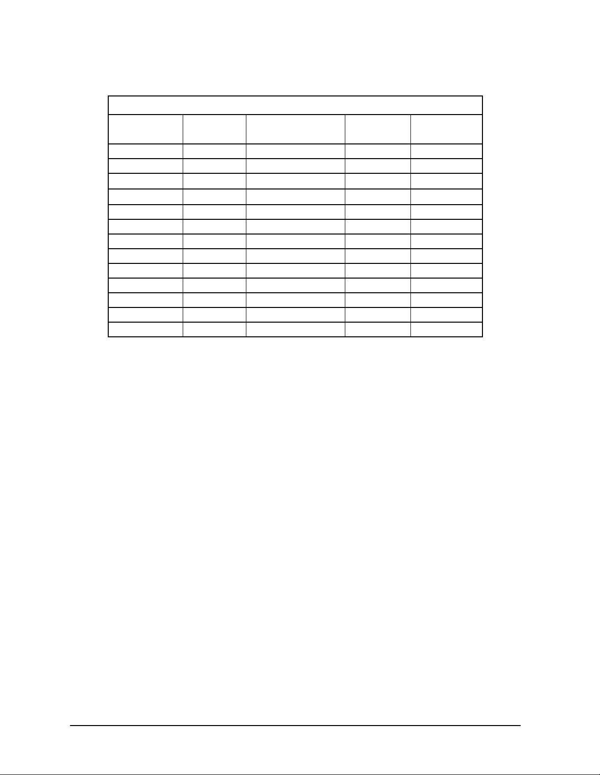
Table 1-2 lists the equipment required to troubleshoot your signal generator. You may use
the recommended model or an equivalent that meets the critical specifications.
Table 1-2 Recommended Test Equipment
Equipment
Digital
Multimeter
Critical Specifications for
Equipment Substitution
Input Resistance: ≤10MΩ Accuracy:
10 mV on 100 V range
Recommended
Model Number
Agilent 3458A
Service Guide 1-11
Page 22
Initial Troubleshooting and RF Block Diagrams ESG Family Signal Generators
Initial Troubleshooting
Initial Troubleshooting
Perform the following troubleshooting steps in the order they are presented. If you are
unable to identify the failed assembly, go to Chapter 2, “Assembly-Level Troubleshooting
with Block Diagrams,” for further instruction.
NOTE Do not attempt to replace any fuses within the power supply to correct a
problem with your signal generator. If you determine that the power supply is
the failed assembly, replace the power supply.
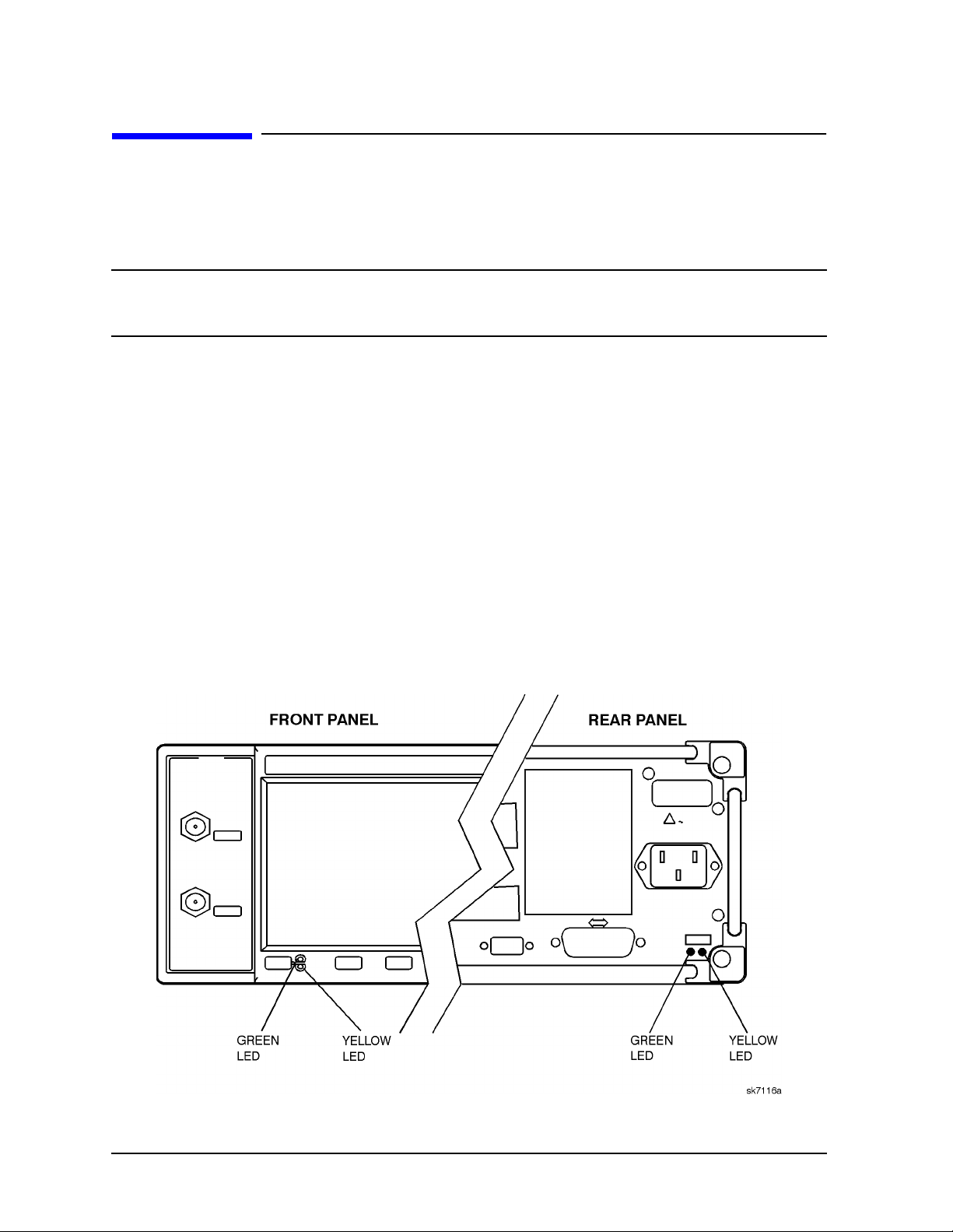
Step 1: Observe the Front and Rear Panel LEDs
Observing the LEDs on the front and rear panel of the signal generator will determine if
there is a catastrophic failure in the power supply assembly.
1. Ensure the signal generator is plugged in (do not switch the power on) and verify that
the yellow LED on both the front and rear panels is lit. Refer to Figure 1-1 for LED
locations. A lit yellow LED (+15 V_STBY) indicates that line voltage is present.
2. Power on the signal generator and verify that the green LED on both the front and rear
panels is lit. A lit green LED indicates the power supply has received an “ON”
command. The ON/OFF switch toggles a flip-flop latch which biases the proper
transistors in the LED control circuit. This circuit is powered by VBAT, the
battery-backed SRAM supply, so that the on-off state is “remembered” even when the
instrument is unplugged.
Figure 1-1 LED Locations on the Front and Rear Panels
1-12 Service Guide
Page 23

ESG Family Signal Generators Initial Troubleshooting and RF Block Diagrams
Initial Troubleshooting
Step 2: Power On the Signal Generator and Check for Error Messages
This procedure verifies that the signal generator powers up and that the internal
instrument check identifies no errors. The internal check evaluates the correctness of
operation and returns an error message if a problem is detected.
1. Switch on the signal generator. Let the signal generator warm up for at least five
minutes.
NOTE For ESG-AP, ESG-DP, and Option 1E5 signal generators, ERROR 514,
Reference Oven Cold will occur whenever the signal generator is powered
up within five minutes of being connected to AC line power. The
annunciator and the ERR annunciator will both turn on. The OVEN COLD
annunciator will automatically clear after approximately five minutes. The
error queue cannot be cleared, however, until the
OVEN COLD annunciator has
turned off.
2. Cycle the power to the signal generator and verify that the green LED on both the front
and rear panels is lit. Refer to Figure 1-1.
OVEN COLD
3. When the display is lit, check to see if the
4. If the
ERR annunciator is turned on, review the error messages in the queue by pressing
Utility > Error Info > View Next Error Message. The first error message in the queue will be
ERR annunciator is turned on.
shown in the text area of the display. Refer to the Error Messages guide for descriptions
of error messages.
If there is more than one error message (each message will be designated as 1 of n),
continue pressing the
View Next Error Message softkey until you have seen and recorded all
of the messages.
5. If you were able to resolve all of the error messages, press Utility > Error Info >
Clear Error Queue(s) to delete the list of error messages.
Service Guide 1-13
Page 24
Initial Troubleshooting and RF Block Diagrams ESG Family Signal Generators
Initial Troubleshooting
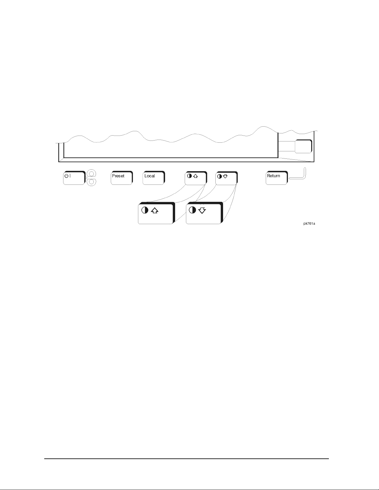
Step 3: Functional Check the Front Panel Keys and Display
1. Press various front panel hardkeys and softkeys to verify they function as expected.
2. Use the contrast keys to verify that the display can be lightened and darkened. Refer to
Figure 1-2.
Figure 1-2 Contrast Keys
1-14 Service Guide
Page 25
ESG Family Signal Generators Initial Troubleshooting and RF Block Diagrams
Initial Troubleshooting
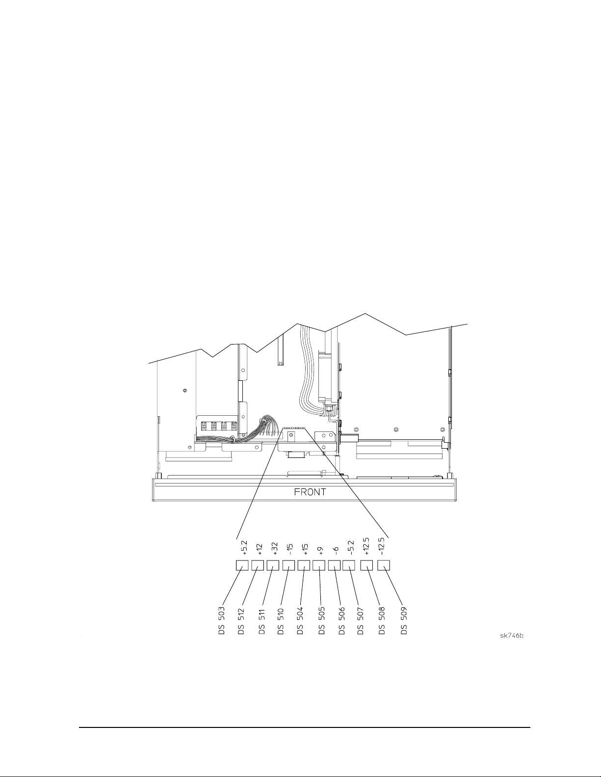
Step 4: Visually Check the Individual Voltage Supplies
1. Unplug the signal generator and remove the instrument cover. Refer to Chapter 5,
“Assembly Replacement,” for removal instructions.
2. Expose the motherboard by removing the top cover. It is secured by 11 screws.
3. Plug in the signal generator and allow it to warm up for at least five minutes.
4. If possible, clear the error queue(s) of messages. Press
Queue(s)
.
Utility > Error Info > Clear Error
5. On the motherboard, locate the 10 LEDs that correspond to the individual voltage
supplies (see Figure 1-3). Verify that all the LEDs are lit. If one or more LEDs are off,
proceed to “Step 6: Isolate the Failed Assembly”.
Figure 1-3 LED Locations on the Motherboard
Service Guide 1-15
Page 26

Initial Troubleshooting and RF Block Diagrams ESG Family Signal Generators
Initial Troubleshooting
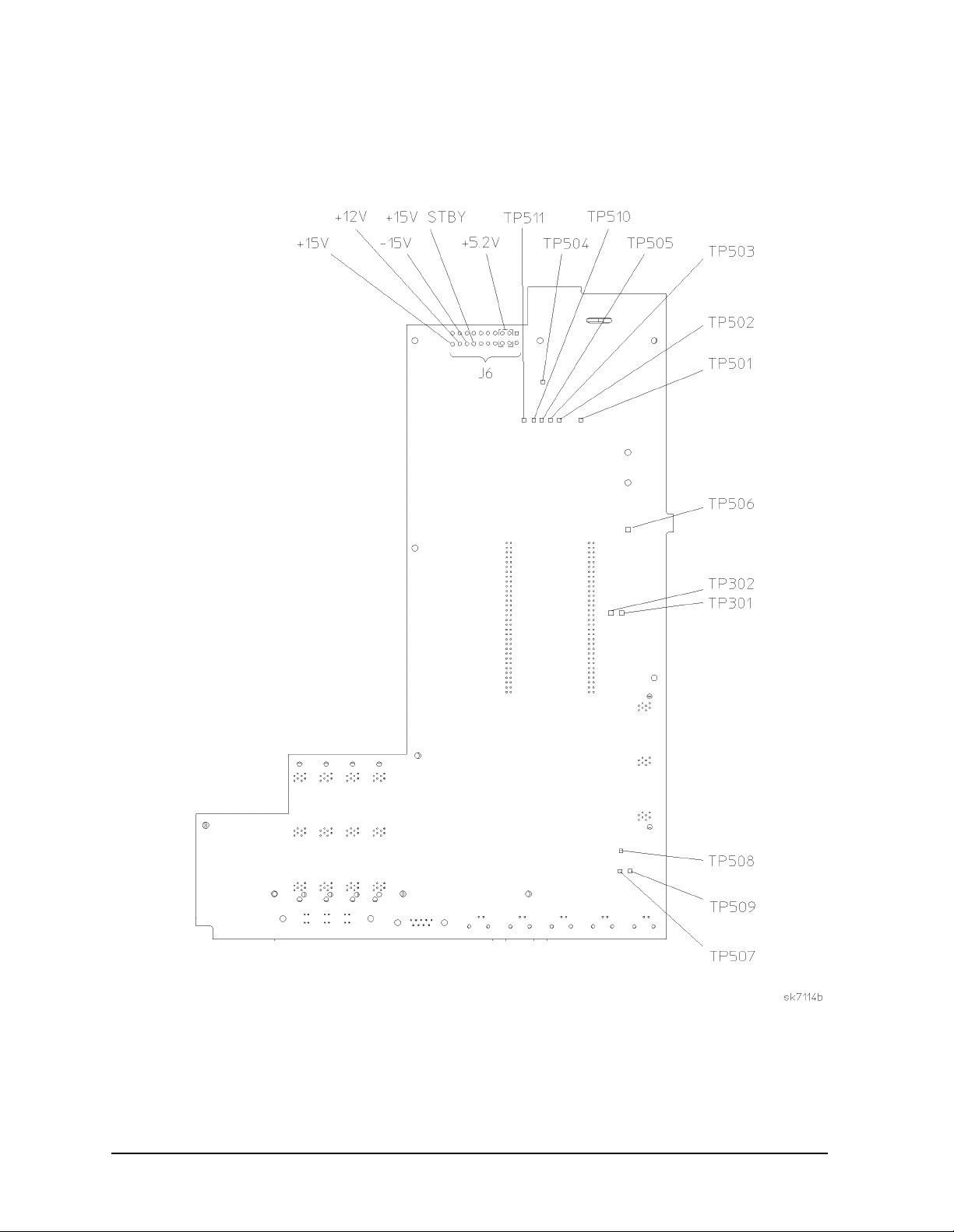
Step 5: Measure the Individual Voltage Supplies
The voltages supplied as inputs from the power supply via J6 to the motherboard are
+15 V (TP502), +15 V standby (+15 V_STBY), −15 V (TP503), +12 V (TP505), and
+5.2 V (TP302). DGND (TP301) is associated with these supplies.
The −6 V (TP508) and −5.2 V (TP509) supplies receive their input from the +5.2 V digital
supply (5.2 VD at TP506). The +5.2 V digital line is filtered to prevent the switching power
supply noise from being induced onto the +5.2 VD supply lines. The −6 V is a bias voltage
for circuits on the output board and other RF circuitry. The −5.2 V is used by the emitter
coupled logic (ECL) digital ICs. The LCD display driver voltage (VLCD), a −14 V to −24 V
source, also receives input from the +5.2 VD supply.
The input to the +32 V supply (TP504) is the +12 V supply.The +32 V supply is used by the
synthesizer/doubler assembly. This supply also includes an LC noise filter.
The +12.5 V regulated supply (TP510) originates from the +15 V input. The −12.5 V
regulated supply (TP511) originates from the −15 V input. These two supplies are used by
the solid-state attenuator and the reverse power protection (RPP). The +10 V reference
(TP501) originates from the +15 V input. The +9 V supply (TP507) originates from the
+10 V reference and the +12 V supply.
1. Unplug the signal generator and turn it upside-down.
2. Expose the motherboard by removing the bottom cover. It is secured by 15 screws.
3. Plug in the signal generator.
4. Measure the voltage of each supply to verify they are within the tolerances listed in
Table 1-3. The voltage supply test point locations are shown in Figure 1-4. If all the
voltages are within tolerance, proceed to “Step 7: Check for Basic CPU Functionality”.
1-16 Service Guide
Page 27
ESG Family Signal Generators Initial Troubleshooting and RF Block Diagrams
Initial Troubleshooting
Table 1-3 Voltage Supply Tolerances
Test Point Supply Voltage Tolerance
J6 (pins 2, 3, 12, 13) +5.2 V +/− 3%
J6 (pin 20) +15 V +/− 3%
J6 (pin 18) −15 V +/− 3%
J6 (pin 19) +12 V +/− 3%
J6 (pin 17) +15 V_STBY +/− 5%
TP301 DGND N/A
TP302 +5.2 V +/− 3%
TP501 +10 V_REF +/− 3%
TP502 +15 V +/− 3%
TP503 −15 V +/− 3%
TP504 +32 V +/− 4%
TP505 +12 V +/− 3%
TP506 +5.2 VD +/− 4%
TP507 +9 V +/− 4%
TP508 −6 V +/− 4%
TP509 −5.2 V +/− 4%
TP510 +12.5 V +/− 4%
TP511 −12.5 V +/− 4%
Service Guide 1-17
Page 28
Initial Troubleshooting and RF Block Diagrams ESG Family Signal Generators
Initial Troubleshooting
Figure 1-4 Motherboard Test Point Locations
1-18 Service Guide
Page 29

ESG Family Signal Generators Initial Troubleshooting and RF Block Diagrams
Initial Troubleshooting
Step 6: Isolate the Failed Assembly
1. Switch off the signal generator.
2. Remove or disconnect an assembly. Below is a suggested order of removal/disconnection
based upon ease.
For the ESG-A and ESG-D Series:
a. A5 Dual Arbitrary Waveform Generator Board (Option UND)
b. A6 Bit Error Rate Test Board (Option UN7)
c. A7 Baseband Generator Board (Options UN3, UN4, UN8, UN9)
d. A8 Data Generator Board (Options UN3, UN4, UN8, UN9)
e. A21 Demodulator Board (Option 300)
f. Front Panel - disconnect A1W1 ribbon cable
g. A3 Inverter - disconnect A3W1
h. A2 Display - disconnect W10
i. AT1 Electronic Attenuator/RPP - disconnect W13
AT1 Mechanical Attenuator and A19 RPP (Option UNB) - disconnect W13 and
A19W1
j. A25 Pulse Modulator (Option 1E6) - disconnect A25W1
k. B1 Fan - disconnect B1W1 (disconnect only temporarily)
l. B2 Fan - disconnect B2W1 (disconnect only temporarily)
m.A9 Output Board
n. A11 Reference Board
o. A12 Synthesizer/Doubler Board
p. A20 YIG Down Convertor Assembly (Option 300) - disconnect W31
NOTE Refer to Chapter 3, “Replaceable Parts (ESG-A and ESG-D Series),” for
information on locating assemblies. Refer to Chapter 5, “Assembly
Replacement,” for information on removing or disconnecting assemblies.
For the ESG-AP and ESG-DP Series:
a. A5 Dual Arbitrary Waveform Generator Board (Option UND)
b. A6 Bit Error Rate Test Board (Option UN7)
c. A7 Baseband Generator Board (Options UN3, UN4, UN8, UN9)
d. A8 Data Generator Board (Options UN3, UN4, UN8, UN9)
e. Front Panel - disconnect A1W1 ribbon cable
f. A3 Inverter - disconnect A3W1
Service Guide 1-19
Page 30

Initial Troubleshooting and RF Block Diagrams ESG Family Signal Generators
Initial Troubleshooting
g. A2 Display - disconnect W10
h. AT1 Electronic Attenuator/RPP - disconnect W13
AT1 Mechanical Attenuator and A19 RPP (Option UNB) - disconnect W13 and
A19W1
i. A25 Pulse Modulator (Option 1E6) - disconnect A25W1
j. B1 Fan - disconnect B1W1 (disconnect only temporarily)
k. B2 Fan - disconnect B2W1 (disconnect only temporarily)
l. A9 Output Board
m.A11 Reference Board
n. A23 Sampler Board
o. A24 Frac-N/Divider Board
p. A22 YIG Driver Assembly - disconnect W35
NOTE Refer to Chapter 4, “Replaceable Parts (ESG-AP and ESG-DP Series),” for
information on locating assemblies. Refer to Chapter 5, “Assembly
Replacement,” for information on removing or disconnecting assemblies.
3. Switch on the signal generator and check the voltage supply LEDs (see Figure 1-3). If
the LEDs are lit, you have likely identified the failed assembly. If one or more LEDs are
still off, switch off the signal generator and replace/reconnect the assembly and repeat
this procedure.
1-20 Service Guide
Page 31

ESG Family Signal Generators Initial Troubleshooting and RF Block Diagrams
Initial Troubleshooting
Step 7: Check for Basic CPU Functionality
The Digital Signal Processor (DSP) performs a self-diagnostic test at power up. If the DSP
is not working, the CPU reports an error.
If the DSP does not seem to be working and the CPU did not report the error, then check
the CLK_OUT signal at TP701. It should be a 16 MHz signal. (Refer to Figure 1-5.)
The eight LEDs of DS201 (see Figure 1-5) indicate the status of the boot and flash ROM for
the CPU. The LEDs form a binary code that can be described as a two digit hexadecimal
code. Table1-4 shows the test sequence and the LED pattern (binary representation) of the
test that is running. If an error occurs and the test is halted, the LED pattern will indicate
which self test halted the process. The LED closest to R201 is the place holder for the Least
Significant Bit (LSB) in the pattern.
Table 1-4 Sequence for DSP Self-Diagnostic Tests
Test Description
LEDs at start of test FF 1111 1111
Checksum test FE 1111 1110
Bootrom RAM test FD 1111 1101
RAM test FC 1111 1100
I/O bus test FB 1111 1011
Main firmware checksum test FA 1111 1010
CPU test AA 1010 1010
Test done and OK 00 0000 0000
Hexadecimal
Code
Binary
Equivalent
MSB LSB
Service Guide 1-21
Page 32

Initial Troubleshooting and RF Block Diagrams ESG Family Signal Generators
Initial Troubleshooting
Figure 1-5 Location of TP701 and DS201-208 on CPU/Motherboard
1-22 Service Guide
Page 33

ESG Family Signal Generators Initial Troubleshooting and RF Block Diagrams
Additional Information for Troubleshooting the ESG-AP and ESG-DP Series
Additional Information for Troubleshooting the
ESG-AP and ESG-DP Series
Table 1-5 provides frequency-dependent settings for selected points in the RF signal flow of
the ESG-AP and ESG-DP Series Signal Generators.Notice that the settings are relative to
the RF output frequency. This information can improve your understanding of the signal
generator circuitry, especially when used with the RF block diagram.
NOTE The values for Table 1-5 assume FM modulation is turned off.
Table 1-5 Frac-N, YO, and Other Selected Frequency-Dependent Settings for Several
RF Output Frequencies
Freq
Out
(MHz)
4000 8000 9 8 593.75000 37.1093750 884.7656250 High 2
3000 6000 7 10 644.53125 32.2265625 852.5390625 High 2
2271 4542 7 10 605.62500 30.2812500 644.5312500 Low 2
1500 6000 7 10 644.53125 32.2265625 852.5390625 High 4
1001 4004 5 10 685.46875 34.2734375 793.9453125 High 4
1000 8000 9 8 593.75000 37.1093750 884.7656250 High 8
700 5600 7 10 847.65625 42.3828125 793.9453125 High 8
300 4800 6 10 726.56250 36.3281250 793.9453125 High 16
240 6080 7 10 603.90625 30.1953125 864.2578125 High 8
100 7200 8 9 928.12500 51.5625000 893.5546875 High 8
1 7992 9 8 887.62500 55.4765625 881.8359375 High 8
Freq
YO
(MHz)
NP
Frac-N
(MHz)
Fif (MHz) Fs (MHz)
Hi/Low
Output
Divider
Service Guide 1-23
Page 34

ESG-A SERIES RF BLOCK DIAGRAM
(STANDARD & OPTION 1E6)
1 GHz REF
LF OUT
A SYNTHESIZER BOARD
.5-1 GHz
F
f
2
Om
/
FM
d/dt
D REFERENCE BOARD
VARIABLE
MODULUS
PRESCALER
FRACTIONAL
DIVIDE
5 MHz
X2
X2
B OUTPUT BOARD
.75-1 GHz
.0-.25 GHz
OPTION 1E6
E PULSE MOD
ALC
.25-4 GHz
MODULATOR
2
ALC
MODULATOR
DRIVER
BURST
MODULATOR
.25-4 GHz
ALC
HOLD
ALC
DETECTOR
50
PULSE
INPUT
C ATTENUATOR
/RPP
DETECTOR
FEED FORWARD AM
SHAPING
ALC REF
5dB STEP
ATTENUATOR
DAC
BURST
MODULATOR
DRIVER
HOLD ALC
ALC_REF
IN_BAND_AM
RPP
RF Out
EXT REF
sk766b
EXT 1
INPUT
EXT 2
INPUT
PLL
10 MHz PLL
10 MHz BW
1 GHz PLL
PLL
NC
FM_MOD
LIN_AM_MOD
PULSE MOD
10 MHz
SYNTH
10 MHz
OUT
1 GHz
REF
LIN_AM_MOD
PULSE MOD
ESG-A SERIES RF BLOCK DIAGRAM
(STANDARD & OPTION 1E6)
Page 35

ESG-D SERIES RF BLOCK DIAGRAM
A SYNTHESIZER BOARD
.5-1 GHz
VARIABLE
MODULUS
PRESCALER
FRACTIONAL
DIVIDE
F
f
5 MHz
2
Om
/
FM
D REFERENCE BOARD
LF OUT
d/dt
10 MHz SYNTH
X2
X2
1 GHz REF
B OUTPUT BOARD
.25-4 GHz
ALC
HOLD
.0-.25 GHz.0-.25 GHz
ALC
DETECTOR
DETECTOR
SHAPING
DAC
C ATTENUATOR
/RPP
5dB STEP
50
ALC REF
ATTENUATOR
RPP
.75-1 GHz.75-1 GHz
AUX
OUT
(COHERENT
CARRIER)
2
.25-4 GHz
VBLO
DAC
QUAD
IQ MODULATOR
90
ALC
MODULATOR
0
ALC
MODULATOR
DRIVER
BURST
MODULATOR
DAC
CAL
VOLTAGE
Q OFFSET
DAC
DAC
Q GAIN
BURST
MODULATOR
DRIVER
FEED FORWARD AM
HOLD ALC
EXT
I INPUT
EXT
Q INPUT
I OFFSET
DAC
DAC
I GAIN
CAL
VOLTAGE
EXT 1
INPUT
EXT 2
INPUT
EXT REF
PLL
10 MHz PLL
10 MHz BW
PLL
1 GHz PLL
FM_MOD
LIN_AM_MOD
PULSE MOD
10 MHz
SYNTH
10 MHz
OUT
1 GHz
REF
ALC_REF
IN_BAND_AM
LIN_AM_MOD
PULSE MOD
sk773b
ESG-D SERIES RF BLOCK DIAGRAM
Page 36

ESG-D SERIES RF BLOCK DIAGRAM
(OPTIONS UN3 & UN4)
1 GHz REF
B OUTPUT BOARD
LF OUT
EXT 1
INPUT
EXT 2
INPUT
EXT REF
A SYNTHESIZER BOARD
.5-1 GHz
Om
/
FM
d/dt
D REFERENCE BOARD
10 MHz BW
10 MHz PLL
PLL
1 GHz PLL
PLL
F
f
VARIABLE
MODULUS
PRESCALER
FRACTIONAL
DIVIDE
5 MHz
2
10 MHz SYNTH
FM_MOD
LIN_AM_MOD
PULSE MOD
10 MHz
SYNTH
10 MHz
OUT
1 GHz
REF
X2
X2
2
10 MHz DIG
EXT 13 MHz
DATA_CLOCK
DATA
EXT_SYNC
EXT_BURST
PATTERN
TRIG
EVENT 1
EVENT 2
AUX
OUT
(COHERENT
CARRIER)
.25-4 GHz
VBLO
DAC
IQ MODULATOR
QUAD
DAC
I OFFSET
DAC
DAC
EXT
I INPUT
EXT
Q INPUT
I GAIN
E BASEBAND GENERATOR BOARD
PLL_LCK_SIG
MASTER_CLK
BUF_DATA_IN
SYMBOL_SYNC
L DATA_CLK
BBG_BIT_CLK
SUB_I_COUNT
L_BURST
SCRAMBLE_RUN
SYMBOL_SYNC
BURST_GATE
INTERNAL DATA
GENERATOR
(PATTERN RAM)
UN3=1M
UN4=8M
DATA
GENERATION
CONTROL
USER_DATA
PLL_CLOCK
SWITCH
MASTER
CLOCK-PLL
DATA
F DATA GENERATOR BOARD
90
DAC
DAC
CONTROL
BURST & DELAY
BURST_PLS
-1V_REF
CAL
VOLTAGE
SWITCH & FILTERS
BURST_PULSE
0
CAL
VOLTAGE
BURST MOD
Q OFFSET
DAC
DAC
Q GAIN
BURST_ENVELOPE
INT_ Q_MOD
INT_ I_MOD
ALC
MODULATOR
ALC
MODULATOR
DRIVER
FEED FORWARD AM
LIN_BURST
MODULATOR
BURST
MODULATOR
DRIVER
LOG_BURST
BURST
HOLD ALC
BURST
ALC_REF
IN_BAND_AM
.75-1 GHz.75-1 GHz
.25-4 GHz
ALC
HOLD
.0-.25 GHz.0-.25 GHz
ALC
DETECTOR
DETECTOR
SHAPING
DAC
C ATTENUATOR
/RPP
5dB STEP
50
ALC REF
ATTENUATOR
RPP
sk774b
LIN_AM_MOD
PULSE MOD
ESG-D SERIES RF BLOCK DIAGRAM (OPTIONS UN3 & UN4)
Page 37

ESG-D SERIES RF BLOCK DIAGRAM
(OPTION UN8 or UN9) Rev C or D
1 GHz REF
B OUTPUT BOARD
LF OUT
EXT 1
INPUT
EXT 2
INPUT
EXT REF
A SYNTHESIZER BOARD
.5-1 GHz
VARIABLE
MODULUS
PRESCALER
FRACTIONAL
DIVIDE
F
f
Om
/
d/dt
FM
10 MHz SYNTH
D REFERENCE BOARD
10 MHz BW
10 MHz PLL
PLL
1 GHz PLL
PLL
5 MHz
2
FM_MOD
LIN_AM_MOD
PULSE MOD
10 MHz
SYNTH
10 MHz
OUT
1 GHz
REF
X2
X2
2
10 MHz DIG
EXT 13 MHz
DATA_CLOCK
DATA
EXT_SYNC
EXT_BURST
PATTERN
TRIGGER
EVENT 1
EVENT 2
AUX
OUT
(COHERENT
CARRIER)
.25-4 GHz
VBLO
DAC
IQ MODULATOR
90
QUAD
DAC
I OFFSET
DAC
DAC
EXT
I INPUT
EXT
Q INPUT
I GAIN
CAL
VOLTAGE
E BASEBAND GENERATOR BOARD
MASTER
CLOCK-PLL
MPU
GLOBAL CLOCK INPUTS
INTERNAL DATA
GENERATOR
(PATTERN RAM)
UN8=1M
UN8&UN9=8M
EVENT1_OUT
USER_DATA_EN
PLL_LCK_SIG
MASTER_CLK
BBG_BIT_CCK
SUB_I_CLK
MPU BUS
DATA
GENERATION
CONTROL
BASEBAND
GEN. I/O
FPGA
FPGA
FPGA
FPGA BUS
DAC
DAC
CONTROL
BURST & DELAY
BURST_PLS
-1V_REF
F DATA GENERATOR BOARD
0
CAL
VOLTAGE
BURST MOD
SWITCH &
FILTERS
BURST_PULSE
Q OFFSET
DAC
DAC
Q GAIN
BURST_ENVELOPE
INT_ Q_MOD
INT_ I_MOD
LIN_AM_MOD
ALC
MODULATOR
ALC
MODULATOR
DRIVER
FEED FORWARD AM
LIN_BURST
PULSE_MOD
BURST
MODULATOR
BURST
MODULATOR
DRIVER
LOG_BURST
.75-1 GHz
HOLD ALC
BURST
ALC_REF
IN_BAND_AM
.25-4 GHz
ALC
HOLD
.0-.25 GHz
DETECTOR
SHAPING
ALC
DETECTOR
DAC
50
ALC REF
C ATTENUATOR
/RPP
5dB STEP
ATTENUATOR
RPP
sk77c
ESG-D SERIES RF BLOCK DIAGRAM (OPTION UN8 or UN9 ) Rev C or D
Page 38

ESG-D SERIES RF BLOCK DIAGRAM (OPTION UN7 with UN8)
1 GHz REF
B OUTPUT BOARD
LF OUT
EXT 1
INPUT
EXT 2
INPUT
EXT REF
A SYNTHESIZER BOARD
.5-1 GHz
Om
/
FM
d/dt
D REFERENCE BOARD
10 MHz BW
10 MHz PLL
PLL
1 GHz PLL
PLL
F
f
VARIABLE
MODULUS
PRESCALER
FRACTIONAL
DIVIDE
5 MHz
2
10 MHz SYNTH
FM_MOD
LIN_AM_MOD
PULSE MOD
10 MHz
SYNTH
10 MHz
OUT
1 GHz
REF
X2
X2
2
10 MHz DIG
EXT 13 MHz
DATA_CLOCK
DATA
EXT_SYNC
EXT_BURST
PATTERN
TRIG
EVENT 1
EVENT 2
AUX
OUT
(COHERENT
CARRIER)
.25-4 GHz
VBLO
DAC
IQ MODULATOR
90
QUAD
DAC
I OFFSET
DAC
DAC
EXT
I INPUT
EXT
Q INPUT
I GAIN
E BASEBAND GENERATOR BOARD (UN8)
PLL_LCK_SIG
MASTER_CLK
BUF_DATA_IN
SYMBOL_SYNC
L DATA_CLK
BBG_BIT_CLK
SUB_I_COUNT
L_BURST
SCRAMBLE_RUN
SYMBOL_SYNC
BURST_GATE
INTERNAL DATA
GENERATOR
(PATTERN RAM)
UN3=1M
UN4=8M
DATA
GENERATION
CONTROL
DAC
DAC
CONTROL
BURST & DELAY
BURST_PLS
-1V_REF
USER_DATA
PLL_CLOCK
SWITCH
MASTER
CLOCK-PLL
DATA
F DATA GENERATOR BOARD
CAL
VOLTAGE
SWITCH & FILTERS
BURST_PULSE
0
CAL
VOLTAGE
BURST MOD
Q OFFSET
DAC
DAC
Q GAIN
BURST_ENVELOPE
INT_ Q_MOD
INT_ I_MOD
ALC
MODULATOR
ALC
MODULATOR
DRIVER
FEED FORWARD AM
LIN_BURST
MODULATOR
BURST
MODULATOR
DRIVER
LOG_BURST
BURST
.25-4 GHz
ALC
HOLD
.0-.25 GHz.0-.25 GHz
ALC
DETECTOR
DETECTOR
SHAPING
.75-1 GHz.75-1 GHz
HOLD ALC
BURST
ALC_REF
IN_BAND_AM
G BERT MEASURMENT BOARD (UN7)
BERT
DATA IN
BERT
CLK IN
BERT
GATE IN
INPUT
BERT ASIC
DSP
BER
Calculation
DAC
50
ALC REF
BER
SYNC LOSS
BER
NO DATA
BER
ERR OUT
BER
TEST OUT
BER
MEAS END
C ATTENUATOR
/RPP
5dB STEP
ATTENUATOR
RPP
sk775b
LIN_AM_MOD
PULSE MOD
ESG-D SERIES RF BLOCK DIAGRAM (OPTION UN7 with UN8)
Page 39

ESG-D SERIES RF BLOCK DIAGRAM
(OPTIONS UN8 or UN9) Rev B
1 GHz REF
B OUTPUT BOARD
LF OUT
EXT 1
INPUT
EXT 2
INPUT
EXT REF
A SYNTHESIZER BOARD
.5-1 GHz
Om
/
FM
d/dt
D REFERENCE BOARD
10 MHz BW
10 MHz PLL
PLL
1 GHz PLL
PLL
F
f
VARIABLE
MODULUS
PRESCALER
FRACTIONAL
DIVIDE
5 MHz
2
10 MHz SYNTH
FM_MOD
LIN_AM_MOD
PULSE MOD
10 MHz
SYNTH
10 MHz
OUT
1 GHz
REF
X2
X2
2
10 MHz DIG
EXT 13 MHz
DATA_CLOCK
DATA
EXT_SYNC
EXT_BURST
PATTERN
TRIG
EVENT 1
EVENT 2
AUX
OUT
(COHERENT
CARRIER)
.25-4 GHz
VBLO
DAC
IQ MODULATOR
QUAD
DAC
I OFFSET
DAC
DAC
EXT
I INPUT
EXT
Q INPUT
I GAIN
E BASEBAND GENERATOR BOARD
PLL_LCK_SIG
MASTER
CLOCK-PLL
DBMIC
DATA
GENERATION
UN8=1M
UN9=8M
CONTROL
BURST & DELAY
USER_DATA
PLL_CLOCK
SWITCH
DATA
MASTER_CLK
BUF_DATA_IN
SYMBOL_SYNC
L DATA_CLK
BBG_BIT_CLK
SUB_I_COUNT
L_BURST
SCRAMBLE_RUN
SYMBOL_SYNC
BURST_GATE
INTERNAL DATA
GENERATOR
(PATTERN RAM)
90
Q
DAC
Q-ADJ
DAC
I-ADJ
I
DAC
CONTROL
CAL
VOLTAGE
BURST_PLS
-1V_REF
0
Q OFFSET
DAC
DAC
Q GAIN
CAL
VOLTAGE
RECONSTRUCTION
FILTER
RECONSTRUCTION
FILTER
BURST MOD
SWITCH & FILTERS
Q-OFFSET
I-OFFSET
BURST_ENVELOPE
.75-1 GHz.75-1 GHz
.0-.25 GHz.0-.25 GHz
C ATTENUATOR
/RPP
ALC
MODULATOR
ALC
MODULATOR
DRIVER
BURST
MODULATOR
.25-4 GHz
ALC
HOLD
ALC
DETECTOR
DETECTOR
SHAPING
5dB STEP
50
ALC REF
ATTENUATOR
DAC
BURST
MODULATOR
DRIVER
FEED FORWARD AM
INT_ Q_MOD
AUD 2
INT_ I_MOD
AUD 1
LIN_BURST
LOG_BURST
HOLD ALC
BURST
ALC_REF
IN_BAND_AM
RPP
sk776b
F DATA GENERATOR BOARD
BURST_PULSE
LIN_AM_MOD
PULSE MOD
ESG-D SERIES RF BLOCK DIAGRAM
(OPTIONS UN8 or UN9) Rev B
Page 40

ESG-D SERIES RF BLOCK DIAGRAM
(OPTION UND)
1 GHz REF
B OUTPUT BOARD
A SYNTHESIZER BOARD
.5-1 GHz
F
Om
/
FM
d/dt
VARIABLE
MODULUS
PRESCALER
FRACTIONAL
DIVIDE
f
10 MHz SYNTH
5 MHz
2
X2
X2
.75-1 GHz.75-1 GHz
.0-.25 GHz.0-.25 GHz
C ATTENUATOR
AUX
OUT
(COHERENT
CARRIER)
.25-4 GHz
2
VBLO
DAC
QUAD
IQ MODULATOR
90
ALC
MODULATOR
0
ALC
MODULATOR
DRIVER
BURST
MODULATOR
.25-4 GHz
ALC
DETECTOR
50
DAC
CAL
VOLTAGE
Q OFFSET
DAC
DAC
Q GAIN
ALC
HOLD
DETECTOR
SHAPING
ALC REF
DAC
BURST
MODULATOR
DRIVER
FEED FORWARD AM
HOLD ALC
EXT
I INPUT
EXT
Q INPUT
I OFFSET
DAC
DAC
I GAIN
CAL
VOLTAGE
/RPP
5dB STEP
ATTENUATOR
RPP
DUAL ARBITRARY WAVEFORM GENERATOR BOARD
LF OUT
EXT 1
INPUT
EXT 2
INPUT
EXT REF
D REFERENCE BOARD
10 MHz BW
10 MHz PLL
PLL
1 GHz PLL
PLL
FM_MOD
LIN_AM_MOD
PULSE MOD
10 MHz
SYNTH
10 MHz
OUT
1 GHz
REF
ARB_REF
CLOCK IN
DATA IN
SYNC IN
PATTERN
TRG
REFERENCE
PLL_CLOCK
SOCLK 1
SOCLK 0
DATA
SWITCH
EXT_CLK
EXT_DATA
EXT_SYNC
PATTERN_TRG
DSP
RAM
MEMORY
POL
LATCH
I/O DATA BUS
PLL_ON
SOCLK 1
SOCLK 0
POL_LATCH
EVENT 1 OUT
EVENT 2 OUT
NSGEND
SQADV
WFCNT
CONTROL
LOGIC
DATA
SEQUENCER
RAM
MEMORY
RAM
DATA
RAM
I/O DATA BUS
Q_OUT
BURST
Q
I
Q
DAC
I
DAC
BURST_PULSE
ALC_REF
IN_BAND_AM
I_OUT
LIN_BURST
LOG_BURST
LIN_AM_MOD
PULSE MOD
sk777b
ESG-D SERIES RF BLOCK DIAGRAM (OPTION UND)
Page 41

ESG-D SERIES RF BLOCK DIAGRAM
(OPTION UN7, UN8/UN9, 300)
1 GHz REF
B OUTPUT BOARD
LF OUT
EXT 1
INPUT
EXT 2
INPUT
EXT REF
A SYNTHESIZER BOARD
.5-1 GHz
VARIABLE
MODULUS
PRESCALER
FRACTIONAL
DIVIDE
F
f
Om
/
d/dt
FM
10 MHz SYNTH
D REFERENCE BOARD
10 MHz BW
10 MHz PLL
PLL
1 GHz PLL
PLL
5 MHz
2
FM_MOD
LIN_AM_MOD
PULSE MOD
10 MHz
SYNTH
10 MHz
OUT
1 GHz
REF
X2
X2
2
10 MHz DIG
EXT 13 MHz
DATA_CLOCK
DATA
EXT_SYNC
EXT_BURST
PATTERN
TRIGGER
EVENT 1
EVENT 2
AUX
OUT
(COHERENT
CARRIER)
.25-4 GHz
VBLO
DAC
IQ MODULATOR
90
QUAD
DAC
I OFFSET
DAC
DAC
EXT
I INPUT
EXT
Q INPUT
I GAIN
CAL
VOLTAGE
E BASEBAND GENERATOR BOARD
MASTER
CLOCK-PLL
MPU
GLOBAL CLOCK INPUTS
INTERNAL DATA
GENERATOR
(PATTERN RAM)
UN8=1M
UN8&UN9=8M
EVENT1_OUT
USER_DATA_EN
PLL_LCK_SIG
MASTER_CLK
BBG_BIT_CCK
SUB_I_CLK
MPU BUS
DATA
GENERATION
CONTROL
BASEBAND
GEN. I/O
FPGA
FPGA
FPGA
FPGA BUS
DAC
DAC
CONTROL
BURST & DELAY
BURST_PLS
-1V_REF
F DATA GENERATOR BOARD
0
CAL
VOLTAGE
BURST MOD
SWITCH &
FILTERS
BURST_PULSE
Q OFFSET
DAC
DAC
Q GAIN
BURST_ENVELOPE
INT_ Q_MOD
INT_ I_MOD
LIN_AM_MOD
ALC
MODULATOR
ALC
MODULATOR
DRIVER
FEED FORWARD AM
LIN_BURST
PULSE_MOD
BURST
MODULATOR
BURST
MODULATOR
DRIVER
LOG_BURST
.75-1 GHz
.25-4 GHz
ALC
HOLD
HOLD ALC
BURST
ALC_REF
IN_BAND_AM
OPTION 300
DEMODULATOR
CLOCK
DATA
GAIN
.0-.25 GHz
C ATTENUATOR
/RPP
5dB STEP
ATTENUATOR
FPGA
DETECTOR
SHAPING
INTERFACE
SWITCH
DETECTOR
PLL
ALC
FPGA
DAC
50
ALC REF
CLK
MEMORY
DSP
CLK
G BERT MEASURMENT BOARD
BERT
DATA IN
BERT
CLK IN
BERT
GATE IN
INPUT
BERT ASIC
DSP
BER
CALCULATION
12
RPP
ADC
26 MHz REF
BER
SYNC LOSS
BER
NO DATA
BER
ERR OUT
BER
TEST OUT
BER
MEAS END
DAC
DOWN CONVERTER
IF
321.4
MHz
F
f
sk7110b
ESG-D SERIES RF BLOCK DIAGRAM (OPTION UN7, UN8/UN9, 300 )
Page 42

ESG-AP SERIES RF BLOCK DIAGRAM (STANDARD &1E6)
A FRAC-N (PART OF FRAC-N/DIVIDER)
10 MHz
SYNTH
FM_MOD
Paren/Tessera
Frac-N
D REFERENCE
LF OUT
10 MHz BW
400-1000
MHz
B YO DRIVER
J3
J4
PRETUNE
FM
CROSS
OVER
DAC
<115 Hz
SCALING
-15V
P/O
P/O
F OUTPUT
1 GHz REF
E DIVIDER (PART OF FRAC-N DIVIDER)
.75-1 GHz
YO
J1
FM
COIL
J1
MAIN
COIL
RF OUT TO
FRAC-N/DIVIDER
J7
4-8 GHz
J8
RF OUT TO
SAMPLER
2-4 GHz
1-2 GHz
2
.5-1 GHz
22 2
.25-4 GHz
.25-.5 GHz
AUX
OUT
(Coherent
Carrier)
EXT
I INPUT
EXT
Q INPUT
VBLO
DAC
IQ MODULATOR
QUAD
DAC
I OFFSET
DAC
DAC
I GAIN
ALC
MODULATOR
90
0
Q OFFSET
ALC
MODULATOR
DRIVER
BURST
MODULATOR
DAC
CAL
VOLTAGE
DAC
Q GAIN
CAL
VOLTAGE
LIN_AM_MOD
FEED FORWARD AM
BURST
MODULATOR
DRIVER
.25-4 GHz
HOLD ALC
.0-.25 GHz
ALC
HOLD
ALC_REF
IN_BAND_AM
ALC
DETECTOR
DETECTOR
SHAPING
DAC
50
ALC REF
PULSE
INPUT
G PULSE MOD
H ATTENUATOR /RPP
5dB STEP
ATTENUATOR
RPP
RF OUTPUT
EXT 1
INPUT
EXT 2
INPUT
EXT 10 MHz
INPUT
10 MHz
PLL
VCO
1 GHz
PLL
100
LIN_AM_MOD
PULSE MOD
1 GHz
J3
1 GHz In
10 MHz
SYNTH
10 MHz
OUT
10 MHz
CLK
1 GHZ
REF
FRAC-N
J1
J6
C SAMPLER
750 MHz
4
PROGRAMMABLE
DIVIDER
750 MHz
256
M
DATA
M
6
4 < M < 51
- -
cw
fm
PULSE MOD
2 P
F
+ / -
¦
P = 8, 9, or 10
cw
fm
750 MHz
30-70 MHz
600-735 MHz
765-900 MHz
2.93 MHz Steps
f
s
f = N * f + f
yo s if
f
if
LO
5 < N < 9
- -
F
¦
IF
S
RF
J3
f
yo
sk781b
ESG-AP SERIES RF BLOCK DIAGRAM (STANDARD & 1E6)
Page 43

ESG-DP SERIES RF BLOCK DIAGRAM
A FRAC-N (PART OF FRAC-N/DIVIDER)
Paren/Tessera
Frac-N
10 MHz BW
400-1000
MHz
LF OUT
10 MHz
SYNTH
FM_MOD
D REFERENCE
B YO DRIVER
J3
J4
PRETUNE
FM
CROSS
OVER
DAC
<115 Hz
SCALING
-15V
P/O
P/O
F OUTPUT
1 GHz REF
E DIVIDER (PART OF FRAC-N DIVIDER)
.75-1 GHz
YO
J1
FM
COIL
J1
MAIN
COIL
RF OUT TO
FRAC-N/DIVIDER
J7
4-8 GHz
J8
RF OUT TO
SAMPLER
2-4 GHz
1-2 GHz
.5-1 GHz
2
22 2
.25-.5 GHz
.25-4 GHz
AUX
OUT
(Coherent
Carrier)
EXT
I INPUT
EXT
Q INPUT
VBLO
DAC
IQ MODULATOR
QUAD
DAC
I OFFSET
DAC
DAC
I GAIN
ALC
MODULATOR
90
0
Q OFFSET
ALC
MODULATOR
DRIVER
BURST
MODULATOR
DAC
CAL
VOLTAGE
DAC
Q GAIN
CAL
VOLTAGE
LIN_AM_MOD
FEED FORWARD AM
BURST
MODULATOR
DRIVER
.25-4 GHz
HOLD ALC
.0-.25 GHz
ALC
HOLD
ALC_REF
IN_BAND_AM
ALC
DETECTOR
DETECTOR
SHAPING
DAC
50
ALC REF
G ATTENUATOR
/RPP
5dB STEP
ATTENUATOR
RPP
RF OUTPUT
EXT 1
INPUT
EXT 2
INPUT
EXT 10 MHz
INPUT
10 MHz
PLL
VCO
1 GHz
PLL
100
LIN_AM_MOD
PULSE MOD
1 GHz
J3
1 GHz In
10 MHz
SYNTH
10 MHz
OUT
10 MHz
CLK
1 GHZ
REF
FRAC-N
J1
C SAMPLER
J6
750 MHz
4
PROGRAMMABLE
DIVIDER
750 MHz
256
M
DATA
M
6
4 < M < 51
- -
cw
fm
PULSE MOD
2 P
F
+ / -
¦
P = 8, 9, or 10
cw
fm
750 MHz
30-70 MHz
600-735 MHz
765-900 MHz
2.93 MHz Steps
f
s
f = N * f + f
yo s if
f
if
LO
5 < N < 9
- -
F
¦
IF
S
RF
J3
f
yo
sk767b
ESG-DP SERIES RF BLOCK DIAGRAM
Page 44

ESG-DP SERIES RF BLOCK DIAGRAM (OPTION UN7)
A FRAC-N (PART OF FRAC-N/DIVIDER)
Paren/Tessera
Frac-N
LF OUT
10 MHz
SYNTH
FM_MOD
D REFERENCE
10 MHz BW
400-1000
MHz
B YO DRIVER
J3
J4
PRETUNE
FM
CROSS
OVER
DAC
<115 Hz
SCALING
-15V
P/O
P/O
F OUTPUT
1 GHz REF
E DIVIDER (PART OF FRAC-N DIVIDER)
.75-1 GHz
YO
J1
FM
COIL
J1
MAIN
COIL
RF OUT TO
FRAC-N/DIVIDER
J7
4-8 GHz
J8
RF OUT TO
SAMPLER
2-4 GHz
1-2 GHz
.5-1 GHz
2
22 2
.25-.5 GHz
.25-4 GHz
AUX
OUT
(Coherent
Carrier)
EXT
I INPUT
EXT
Q INPUT
VBLO
DAC
IQ MODULATOR
QUAD
DAC
I OFFSET
DAC
DAC
I GAIN
ALC
MODULATOR
90
0
Q OFFSET
ALC
MODULATOR
DRIVER
BURST
MODULATOR
DAC
CAL
VOLTAGE
DAC
Q GAIN
CAL
VOLTAGE
LIN_AM_MOD
FEED FORWARD AM
BURST
MODULATOR
DRIVER
.25-4 GHz
HOLD ALC
.0-.25 GHz
ALC
HOLD
ALC_REF
IN_BAND_AM
ALC
DETECTOR
DETECTOR
SHAPING
DAC
50
ALC REF
G ATTENUATOR
/RPP
5dB STEP
ATTENUATOR
RPP
RF OUTPUT
EXT 1
INPUT
EXT 2
INPUT
EXT 10 MHz
INPUT
10 MHz
PLL
VCO
1 GHz
PLL
100
LIN_AM_MOD
PULSE MOD
BURST_PULSE
10 MHz SYNTH
10 MHz OUT
10 MHz CLK
1 GHZ REF
1 GHz
J3
FRAC-N
1 GHz In
J6
J1
C SAMPLER
750 MHz
4
PROGRAMMABLE
DIVIDER
750 MHz
256
M
DATA
M
6
4 < M < 51
- -
cw
fm
PULSE MOD
2 P
F
+ / -
¦
P = 8, 9, or 10
cw
fm
750 MHz
30-70 MHz
600-735 MHz
765-900 MHz
2.93 MHz Steps
f
s
f = N * f + f
yo s if
f
if
LO
5 < N < 9
- -
F
¦
10 MHz DIG
EXT 13 MHz
IF
H BASEBAND GENERATOR BOARD
PLL_LCK_SIG
MASTER_CLK
BUF_DATA_IN
SYMBOL_SYNC
DATA
GENERATION
CONTROL
PLL_CLOCK
MASTER
CLOCK-PLL
DAC
DAC
INT_ Q_MOD
INT_ I_MOD
S
RF
J3
f
yo
DATA_CLOCK
DATA
EXT_SYNC
EXT_BURST
PATTERN
TRIG
EVENT 1
EVENT 2
USER_DATA
DATA
SWITCH
L DATA_CLK
BBG_BIT_CLK
SUB_I_COUNT
L_BURST
SCRAMBLE_RUN
SYMBOL_SYNC
BURST_GATE
INTERNAL DATA
GENERATOR
(PATTERN RAM)
UN3=1M
UN4=8M
CONTROL
BURST & DELAY
BURST_PLS
-1V_REF
BURST MOD
SWITCH & FILTERS
BURST_ENVELOPE
K BERT MEASURMENT BOARD
BERT
DATA IN
BERT
CLK IN
BERT
GATE IN
INPUT
BERT ASIC
DSP
BER
Calculation
BER
SYNC LOSS
BER
NO DATA
BER
ERR OUT
BER
TEST OUT
BER
MEAS END
sk782b
J DATA GENERATOR BOARD
BURST_PULSE
ESG-DP SERIES RF BLOCK DIAGRAM (OPTION UN7)
Page 45

ESG-DP SERIES RF BLOCK DIAGRAM (OPTIONS UN8 or UN9)
A FRAC-N (PART OF FRAC-N/DIVIDER)
Paren/Tessera
Frac-N
10 MHz BW
LF OUT
10 MHz
SYNTH
FM_MOD
D REFERENCE
400-1000
MHz
B YO DRIVER
J3
J4
PRETUNE
FM
CROSS
OVER
DAC
<115 Hz
SCALING
-15V
P/O
P/O
F OUTPUT
1 GHz REF
E DIVIDER (PART OF FRAC-N DIVIDER)
.75-1 GHz
YO
J1
FM
COIL
J1
MAIN
COIL
RF OUT TO
FRAC-N/DIVIDER
J7
4-8 GHz
J8
RF OUT TO
SAMPLER
2-4 GHz
1-2 GHz
.5-1 GHz
2
22 2
.25-.5 GHz
.25-4 GHz
AUX
OUT
(Coherent
Carrier)
EXT
I INPUT
EXT
Q INPUT
VBLO
DAC
IQ MODULATOR
QUAD
DAC
I OFFSET
DAC
DAC
I GAIN
ALC
MODULATOR
90
0
Q OFFSET
ALC
MODULATOR
DRIVER
BURST
MODULATOR
DAC
CAL
VOLTAGE
DAC
Q GAIN
CAL
VOLTAGE
LIN_AM_MOD
FEED FORWARD AM
BURST
MODULATOR
DRIVER
.25-4 GHz
HOLD ALC
.0-.25 GHz
ALC
HOLD
ALC_REF
IN_BAND_AM
ALC
DETECTOR
DETECTOR
SHAPING
DAC
50
ALC REF
G ATTENUATOR
/RPP
5dB STEP
ATTENUATOR
RPP
RF OUTPUT
EXT 1
INPUT
EXT 2
INPUT
EXT 10 MHz
INPUT
10 MHz
PLL
VCO
1 GHz
PLL
100
LIN_AM_MOD
PULSE MOD
BURST_PULSE
10 MHz SYNTH
10 MHz OUT
10 MHz CLK
1 GHZ REF
1 GHz
J3
J6
FRAC-N
J1
1 GHz In
C SAMPLER
750 MHz
4
PROGRAMMABLE
DIVIDER
750 MHz
256
M
DATA
M
6
4 < M < 51
- -
cw
fm
PULSE MOD
H BASEBAND GENERATOR BOARD
2 P
F
+ / -
¦
P = 8, 9, or 10
cw
fm
750 MHz
30-70 MHz
600-735 MHz
765-900 MHz
2.93 MHz Steps
f
s
f = N * f + f
yo s if
f
if
LO
5 < N < 9
- -
F
¦
IF
10 MHz DIG
EXT 13 MHz
S
RF
J3
f
yo
DATA_CLOCK
DATA
EXT_SYNC
EXT_BURST
PATTERN
TRIGGER
EVENT 1
EVENT 2
INTERNAL DATA
GENERATOR
(PATTERN RAM)
UN8=1M
UN8&UN9=8M
MASTER
CLOCK-PLL
MPU
GLOBAL CLOCK INPUTS
EVENT1_OUT
USER_DATA_EN
PLL_LCK_SIG
MASTER_CLK
BBG_BIT_CCK
SUB_I_CLK
MPU BUS
DATA
GENERATION
CONTROL
BASEBAND
GEN. I/O
FPGA
FPGA
FPGA
FPGA BUS
DAC
DAC
CONTROL
BURST & DELAY
BURST_PLS
-1V_REF
BURST MOD
SWITCH &
FILTERS
INT_ Q_MOD
INT_ I_MOD
BURST_PULSE
J DATA GENERATOR BOARD
BURST_PULSE
sk783b
ESG-DP SERIES RF BLOCK DIAGRAM (OPTIONS UN8 or UN9)
Page 46

ESG-DP SERIES RF BLOCK DIAGRAM (OPTION UND)
A FRAC-N (PART OF FRAC-N/DIVIDER)
Paren/Tessera
Frac-N
LF OUT
10 MHz
SYNTH
FM_MOD
D REFERENCE
10 MHz BW
400-1000
MHz
B YO DRIVER
J3
J4
PRETUNE
FM
CROSS
OVER
DAC
<115 Hz
SCALING
-15V
P/O
P/O
F OUTPUT
1 GHz REF
E DIVIDER (PART OF FRAC-N DIVIDER)
.75-1 GHz
YO
J1
FM
COIL
J1
MAIN
COIL
RF OUT TO
FRAC-N/DIVIDER
J7
4-8 GHz
J8
RF OUT TO
SAMPLER
2-4 GHz
1-2 GHz
.5-1 GHz
2
22 2
.25-.5 GHz
.25-4 GHz
AUX
OUT
(Coherent
Carrier)
EXT
I INPUT
EXT
Q INPUT
VBLO
DAC
IQ MODULATOR
QUAD
DAC
I OFFSET
DAC
DAC
I GAIN
ALC
MODULATOR
90
0
Q OFFSET
ALC
MODULATOR
DRIVER
BURST
MODULATOR
DAC
FEED FORWARD AM
LIN_BURST
BURST
MODULATOR
DRIVER
LOG_BURST
CAL
VOLTAGE
DAC
Q GAIN
CAL
VOLTAGE
LIN_AM_MOD
.25-4 GHz
HOLD ALC
.0-.25 GHz
ALC
HOLD
ALC_REF
IN_BAND_AM
ALC
DETECTOR
DETECTOR
SHAPING
DAC
50
ALC REF
G ATTENUATOR
/RPP
5dB STEP
ATTENUATOR
RPP
RF OUTPUT
EXT 1
INPUT
EXT 2
INPUT
EXT 10 MHz
INPUT
10 MHz
PLL
VCO
1 GHz
PLL
100
LIN_AM_MOD
PULSE MOD
BURST_PULSE
10 MHz
SYNTH
10 MHz
OUT
10 MHz
CLK
1 GHZ
REF
1 GHz
J3
FRAC-N
1 GHz In
J6
J1
C SAMPLER
750 MHz
4
PROGRAMMABLE
DIVIDER
750 MHz
256
M
DATA
M
6
4 < M < 51
- -
cw
fm
PULSE MOD
2 P
F
+ / -
¦
P = 8, 9, or 10
cw
fm
750 MHz
30-70 MHz
600-735 MHz
765-900 MHz
2.93 MHz Steps
f
s
f = N * f + f
yo s if
f
if
LO
5 < N < 9
- -
F
¦
ARB_REF
IF
S
RF
J3
f
yo
CLOCK IN
DATA IN
SYNC IN
PATTERN
TRG
H DUAL ARBITRARY WAVEFORM GENERATOR BOARD
DSP
RAM
I/O DATA BUS
PLL_ON
SOCLK 1
SOCLK 0
POL_LATCH
EVENT 1 OUT
EVENT 2 OUT
NSGEND
SQADV
WFCNT
CONTROL
LOGIC
DATA
SEQUENCER
RAM
MEMORY
Q
RAM
DATA
I
RAM
I/O DATA BUS
Q
DAC
I
DAC
REFERENCE
PLL_CLOCK
SOCLK 1
SOCLK 0
DATA
SWITCH
EXT_CLK
EXT_DATA
EXT_SYNC
PATTERN_TRG
MEMORY
POL
LATCH
Q_OUT
I_OUT
sk784b
BURST_PULSE
ESG-DP SERIES RF BLOCK DIAGRAM (OPTION UND)
Page 47

ESG Family Signal Generators
2Assembly-Level Troubleshooting with
Block Diagrams
This chapter provides the block diagrams and information necessary for you to test and
troubleshoot the major assemblies of your signal generator.
Service Guide 2-1
Page 48

Assembly-Level Troubleshooting with Block Diagrams ESG Family Signal Generators
Before You Begin Troubleshooting
Before You Begin Troubleshooting
Be sure to review the warning and caution statements described in Chapter 7 prior to
troubleshooting your signal generator.
Using this Chapter with Service Software
Some block diagrams in this chapter are accompanied by a table for use with the
automated service software that came with your signal generator. These tables list the
signal generator’s test conditions and the expected ABUS node voltages. The service
software has a utility program which measures and displays the node voltages for each
test. Refer to your signal generator’s calibration guide for information on using the
software.
The block diagrams and ABUS node tables are arranged in the following order:
A5 Dual Arbitrary Waveform Generator Block Diagram (Option UND)
A6 Bit Error Rate Test Block Diagram (Option UN7)
A7 Baseband Generator Block Diagram (Options UN3 & UN4)
A7 DBMIC Baseband Generator Block Diagram (Options UN8 & UN9)
A8 Data Generator Block Diagram (Options UN3 & UN4)
A8 Data Generator - Rev. A & B Block Diagram (Options UN8 & UN9)
A8 Flex Data Generator - Rev. C & D Block Diagram (Options UN8 & UN9)
A9 Output ABUS Nodes (ESG-A Series)
A9 Output Block Diagram (ESG-A Series)
A9 Output ABUS Nodes (ESG-D Series)
A9 Output ABUS Nodes (ESG-AP, & ESG-DP Series)
A9 Output Block Diagram (ESG-D, ESG-AP, & ESG-DP Series)
A11 Reference ABUS Nodes (ESG-A & ESG-D Series)
A11 Reference Block Diagram (ESG-A & ESG-D Series)
A11 Reference ABUS Nodes (ESG-AP & ESG-DP Series)
A11 Reference Block Diagram (ESG-AP & ESG-DP Series)
A12 Synthesizer/Doubler ABUS Nodes (ESG-A & ESG-D Series)
A12 Synthesizer/Doubler Block Diagram (ESG-A & ESG-D Series)
A14 CPU/Motherboard ABUS Nodes
2-2 Service Guide
Page 49

ESG Family Signal Generators Assembly-Level Troubleshooting with Block Diagrams
Using this Chapter with Service Software
A14 CPU/Motherboard Block Diagram (1 of 2)
A14 CPU/Motherboard Block Diagram (2 of 2)
A20 Downconvertor Block Diagram (Option 300)
A21 Demodulator Block Diagram (Option 300)
A22 YIG Driver ABUS Nodes (ESG-AP & ESG-DP Series)
A22 YIG Driver Block Diagram (ESG-AP & ESG-DP Series)
A23 Sampler ABUS Nodes (ESG-AP & ESG-DP Series)
A23 Sampler Block Diagram (ESG-AP & ESG-DP Series)
A24 Frac-N/Divider ABUS Nodes (ESG-AP & ESG-DP Series
A24 Frac-N/Divider Block Diagram (ESG-AP & ESG-DP Series
AT1 Electronic Attenuator/RPP Block Diagram
AT1 Mechanical Attenuator and A19 RPP Block Diagram (Option UNB)
ESG-A Series Power Supply and Ground Interconnects Block Diagram
ESG-D Series Power Supply and Ground Interconnects Block Diagram (1 of 2)
ESG-D Series Power Supply and Ground Interconnects Block Diagram (2 of 2)
ESG-A Series Modulation and Signal Interconnects Block Diagram
ESG-D Series Modulation and Signal Interconnects Block Diagram (1 of 2)
ESG-D Series Modulation and Signal Interconnects Block Diagram (2 of 2)
Service Guide 2-3
Page 50

A5 DUAL ARBITRARY WAVEFORM GENERATOR BLOCK DIAGRAM (OPTION UND)
REFERENCE
PROCESSOR INTERFACE
P2 - 33
P2-82
P2-83
P2-32
P2-24
P2-74
P2-25
P2 - 26
P2-76
P2-27
P2-77
P2-78
P2-29
P2-79
P2-36
P2-19
P2-20
P2-70
P2-21
P2-71
P2-72
P2-23
P2-73
sk73b
EXT_LSEL
EXT LSTROBE
EXT RD L WR
EXT RESET
IAB0
IAB1
IAB2
IAB3
IAB4
IAB5
IAB6
IAB7
IAB8
IAB9
IAB10
EXT_DO
EXT_D1
EXT_D2
EXT_D3
EXT_D4
EXT_D5
EXT_D6
EXT_D7
SELECT
STROBE
READ/LWRITE
RESET
A0
A1
A2
A3
A4
A5
A6
A7
A8
A9
A10
D0
D1
D2
D3
D4
D5
D6
D7
J3
CLK
SELECT
EEPROM
DATA
CONTROL
LOGIC
LATCHED
ADDRESS
LATCHED
DATA
DIG BUS INT
(PLL UNLOCKED)
POWER SUPPLY INPUTS
P2-9
P2-14,64
+10V
REF
P2-16,66
P2-17,67
P2-12, 62
P2-13,63
P2-1,7,54,56
P2-22,28,34, 40,
46,69,75,81,
87,93 ,99
EXT_REF_DIV4
PLL_REF_CLK
EXT_REF_DEL
ARB_REF
WF_ CLK_RAM
PROCESSOR
+10 VREF
40 Mhz
ABUS
REF SELECT
&
DIVIDE
CLK_IN
DATA BUS
+32V
+15V
-1 VREF
-1 VREF
+5VA
+5.2V
-5.2V
-15V
ANALOG
COMMON
DIGITAL
COMMON
PLL_REF
13 MHz_BBG
WF_CLK_DDS
WAVEFORM
CLOCK
TUNING
USO_CLK 0
DIGITAL
SIGNAL
PROCESSOR
P_RAM
512 Kbyte
FLASH
MEMORY
5 Mbyte
1
K
CL
_
SO
U
NWF_CLK_DIV2
WF_CLK
WF_CLK_DIV2
I_LATCH_CLK
Q_LATCH_CLK
MEMORY DATA BUS
VPPI_EN
VPPQ_EN
DATA SWITCH
CLOCK IN
P2-50
DATA I N
P2-49
SYNC IN
P2-100
PATTER
TRIGGER
P1-4
SQ_CLK0
SQ_CLK1
CLOCK
SELECT
DATA
SELECT
SYNC
SELECT
TRIGGER
SELECT
VPPI_EN
VPPQ_EN
CON_TRISTATE
EXT_CK_POL
DATA_IN_POL
SYNC_IN__POL
PAT_TRIG__POL
POL
LATCH
WF_CLK
WF_CLK_DIV2
POL_LATCH_ENABLE
EVENT 1_OUT
EVENT 2_OUT
EVENT 1
EVENT 2
CLOCK PLL
P1-8
P1-10
RFCLK_DIV
F
PLL_REF
DATA SEQUENCER
VPPI_EN
VPPQ_EN
CONTROL
LOGIC
(FPGA)
EXT_CLOCK
EXT_DATA
EXT_SYNC
PATTERIN_TRIG
SQ_CLK0+
SQ_CLK1
CONTROL
MEMORY
PLL_UNLK
PLL_UNLK
NSGEND
SQADV
WFCNT
I/O DATA BUS
PLL_VCO_TUNE
I/O DATA BUS
75 T O 150 MHz
VCO
PLL_ON
PLL_ON
SQ_CLK0
SQ_CLK1
WF_CLK_DDS_LD
WF_CLK_DDS_UD
WFCLK
FREQ SCALING
WF_CLK_DDS_LD
WF_CLK_DDS_UD
I/O DATA
BUS
SEQUENCER
SEQUENCER
RAM
MEMORY
EVENT 1
EVENT 2
NWFCLK_DIV2
WFCLK_DIV2
Q DATA
GENERATION
WFR_ARB
Q_LATCH_CLK
MEMORY DATA BUS
I/O DATA BUS
CONN_TRISTATE
I DATA
GENERATION
WFR_ARB
MEMORY DATA BUS
NWFCLK_DIV2
WFCLK_DIV2
WAVEFORM
Q RAM
1 Mword
ADJ
DAC
I_LATCH_CLK
WAVEFORM
I RAM
1 Mword
14
Q
OFFSET ADJUST
Q
GAIN ADJUST
I
GAIN ADJUST
I
OFFSET ADJUST
14
WAVEFORM
Q
DAC
WAVEFORM
I
DAC
2X
2X
RECONSTRUCTION
FILTERS
2.50 Khz
2.5 Mhz
8.0 MHz
RECONSTRUCTION
FILTERS
2.50 Khz
2.5 Mhz
8.0 MHz
ABUS
J2
Q_OUT
P2--53
AUD 2
P2-4
J1
I_0UT
P2-52
AUD 2
P2--55
P2-6
16 Mhz
Q_OFFSET
I_OFFSET
16 Mhz
A5 DUAL ARBITRARY WAVEFORM GENERATOR BLOCK DIAGRAM (OPT UND)
Page 51

ESG Family Signal Generators Assembly-Level Troubleshooting with Block Diagrams
A6 Bit Error Rate Test Block Diagram (Option UN7)
A6 Bit Error Rate Test Block Diagram (Option UN7)
Service Guide 2-7
Page 52

A7 BASEBAND GENERATOR BLOCK DIAGRAM (OPTIONS UN3 & UN4)
REFERENCE
P301-84
FROM MOTHERBOARD
FROM 13 MHz IN
/CPU
13 MHz
10 MHz DIG
P403
GENERATOR INTERFACE
P300-6
P300-8
P300-10
P300-12
P300-14
P300-18
P300-20
BURST_GATE
ADJ_TS_PWR_IN
BB_DATA
SYMBOL_SYNC
EXT_CLK
BBG_INT_CLK
BBG_EN
REF SELECT
&
DIVIDE
6
8
10
12
14
18
20
PLL_CLOCK
16
22
L_BURST
BUFFERED_DATA_IN
SYMBOL_SYNC_INV
BBG_BIT_CLK
SUB_I_COUNT (1)
MASTER CLOCK PLL
PLL LOCK SIG
PLL CLK
PLL REF
DATA
ABUS
RC TIME
CONSTANT
LCLK
ABUS
RC TIME
CONSTANT
LDATA_CLK
P300-16
P300-22
P301-35
DIG BUS INT
(PLL UNLOCKED)
PLL_T UNE
ABUS
PLL T UNE
F
REF
LOOP FILTER
&
LEAD/LAG
DATA GENERATION CONTROL
MASTER CLOCK
LBIT_CLK
BUFFERED DATA
SYMBOL SYNC INV
PMF CONTROL
ENCODE
160 T O 320 MHz
LOOP
COUNT
&
DIFF
VCO
VCO
ENABLE
PLL LOCK SIG
SUB_ I_COUNT (3)
p
/4 CLK
CA ADDRESS & CONTROL
SUB_I _COUNT (1)
LATCH ADDRESS
LATCH DATA
PLL
DIVIDERS
20 T O
40 MHz
PMF
CONTROL
LOGIC
LDATA_CLK
p
/4 CONTROL LOGIC
P300-22
LBIT_CLK
L_BURST
CONTROL
LOGIC
MASTER CLOCK
INTERNAL
CLK
BURST PLS
MOD INVERT
CAL ENABLE
LATCH I CAL
LATCH Q CAL
PLL GAIN
EXT REF ENABLE
p
/4 PMF ENABLE
CA PMF ENABLE
VCO ENABLE
EVENT SELECT
BBG_BIT_CLK
LBIT_CLK
PMF CONTROL
P300-16
BURST
CONTROL LOGIC
FORMAT SELECT
PATH
CONTROL LOGIC
I DATA GENERATION
LATCH I CAL
WRITE DATA
p
/4 CLK
FORMAT SELECT
p
/4 CONTROL LOGIC
FORMAT SELECT
CA ADDRESS & CONTROL
12
Q DATA GENERATION
LATCH Q CAL
WRITE DATA
p
/4 CLK
FORMAT SELECT
p
/4 CONTROL LOGIC
FORMAT SELECT
CA ADDRESS & CONTROL
12
BURST MOD
BURST_PLS
CONTROL
LOGIC
15
ENVL_LATCH
LATCH_DATA
BURST_TC
MASTER_CLK
BURST
ENVELOPE
CONTROL
&
RAM
I
CAL LATCHES
I
p
/4 DQPSK
(NADC,TETRA,
PDC,PHS)
I
CONSTANT
AMPLITUDE
(GMSK, GFSK
DECT)
Q
CAL LATCHES
Q
/4 DQPSK
p
(NADC,TETRA,
PDC,PHS)
Q
CONSTANT
AMPLITUDE
(GMSK,GFSK,
DECT)
15
ENVELOPE
DATA
DAC_EN
-IV_REF
I DAC
DATA
MODULATION
ENABLE/SELECT
Q DAC
DATA
MODULATION
ENABLE/SELECT
BURST
ABUS
BURST MOD
SWITCH
AND
FILTERS
12
DAC
12
MOD
INVERT
MOD INVERT
BURST_ENVELOPE
BURST_PULSE
INTL_ALC_HOLD
L_DCC_ALT_PWR_SEL
DAC
ANALOG FILTERS
(NADC/TETRA/
PDC,PHS,GSM)
PATH CONTROL
LOGIC
P301-57
P301-30
P301-31
P301-80
ANALOG FILTERS
(NADC/TETRA/
PDC,PHS GSM)
PATH CONTROL
LOGIC
I OUT
ABUS
Q OUT
ABUS
P405
I OUT
TO I-OUT
INT I MOD OUT
P301-2
P404
Q OUT
TO Q-OUT
INT Q MOD OUT
P301-53
DIGITAL INTERFACE
P301-33
P301-82
P301-83
P301-32
P301-24
P301-74
P301-25
P301-26
P301-76
P301-27
P301-77
P301-78
P301-29
P301-79
P301-36
P301-19
P301-20
P301-70
P301-21
P301-71
P301-72
P301-23
P301-73
EXT SELECT
L EXT STROBE
EXT RD L WR
EXT RESET
IAB0
IAB1
IAB2
IAB3
IAB4
IAB5
IAB6
IAB7
IAB8
IAB9
IAB10
EXT_DO
EXT_D1
EXT_D2
EXT_D3
EXT_D4
EXT_D5
EXT_D6
EXT_D7
POWER SUPPLY INPUTS
P301-9
P301-14,64
+10V
REF
P301-16,66
P301-17,67
P301-12
P301-62
P301-13,63
P301-1,7,54,56
P301-22,28,34,
40,46,69,75,81,
87,93 ,99
SELECT
STROBE
READ/LWRITE
RESET
A0
A1
A2
A3
A4
A5
A6
A7
A8
A9
A10
D0
D1
D2
D3
D4
D5
D6
D7
+10 VREF
CLK
SELECT
DATA
DIG BUS INT
(PLL UNLOCKED)
ABUS
EEPROM
CONTROL
LOGIC
LATCHED
ADDRESS
LATCHED
DATA
+32V
+15V
-1V_REF
-1 V_REF
+5VA
+5.2V
-5.2V
-5V
-15V
ANALOG
COMMON
DIGITAL
COMMON
sk7120a
A7 BASEBAND GENERATOR BLOCK DIAGRAM (OPTIONS UN3 & UN4)
Page 53

A7 DBMIC BASEBAND GENERATOR BLOCK DIAGRAM (OPTIONS UN8 and UN9)
REFERENCE
P1-84
FROM MOTHERBOARD
/CPU
13 MHz
10 MHz DIG
J3
P403
REF SELECT
DIVIDE
GENERATOR INTERFACE
P3-6
P3-8
P3-10
P3-12
P3-14
P3-18
P3-20
P1-85
P1-49
P1-100
P1-50
P2-6
P2-4
P10-8,9,
10,11,12,
13,14,15
P6-12,13,
14,15,16,
17,18,19
BURST_GATE LINT_CLK_EN
ADJ_TS LEXT_CLK_EN
EXT_DATA LBBG_EN
EXT_SYNC
EXT_CLK
BBG_INT_CLK
BBG_EN
BBG_TRIG_INT
DATA
SYNC
CLK
ALT_PWR_IN
PATTERN_TRG
I_DIRECT
Q_DIRECT
6
8
10
12
14
18
20
BURST MOD
MASTER CLOCK PLL
BURST_PLS
CONTROL
LOGIC
15
ENVL_LATCH
LATCH_DATA
BURST_TC
MASTER_CLK
L_BURST
+10V_REF
ALC_HOLD_DIR
BURST_PULSE_DIR
ALT_PWR_DIR
ADJ_TS_PWR_IN
BURST
ENVELOPE
CONTROL
&
RAM
15
ENVELOPE
DATA
DAC_EN
LOOP FILTER
&
LEAD/LAG
DIG_BUS_INT
(PLL UNLOCKED)
PLL_T UNE
ABUS
PLL T UNE
60 T O 120 MHz
VCO
VCO
ENABLE
PLL
DIVIDERS
30 T O
60 MHz
MASTER CLOCK
P1-35
PLL LOCK SIG
PLL CLK
&
PLL REF
LCLK
ABUS
F
REF
DIGITAL MODULATOR IC
BURST
ABUS
BURST MOD
SWITCH
AND
FILTERS
BURST_ENVELOPE
BURST_PULSE
INTL_ALC_HOLD
L_DCC_ALT_PWR_SEL
P1-57
P1-30
P1-31
P1-80
Q DATA
PLL_CLOCK
BBG_BIT_CLK
16
EXT_BURST
2
BURST_GATE
ADJ_TS_PWR_IN
L_BURST
RC TIME
CONSTANT
DATA
ABUS
RC TIME
CONSTANT
BUFFERED_DATA_IN
SYMBOL_SYNC
P3-16
P2-2
FIR
PRE-MOD
FILTER
DATA/SYMBOL
GENERATOR
DIGITAL
INTERPOLATOR
GENERATION
14
CLK_OUT
DATA_OUT
SYNC_OUT
LATCH DATA BUS
DATA_EN_OUT
EVENT1_OUT
I DATA
GENERATION
14
P2-14
P2-12
P2-16
P2-10
P2-8
Q
DAC
ADJ
DAC
DAC
I
14 MHz
Q
OFFSET ADJUST
Q
GAIN ADJUST
I
GAIN ADJUST
I
OFFSET ADJUST
14 MHz
RECONSTRUCTION
FILTER
RECONSTRUCTION
FILTER
Q_OFFSET
I_OFFSET
ABUS
J2
Q_OUT
P1-53
AUD 2
P1-4
J1
I_OUT
P1-2
AUD 1
P1-55
P1-6
POWER SUPPLY INPUTS
P1-9
P1-14,64
+10V
REF
P1-16
P1-17,66,67
P1-12
P1-62
P1-13,63
P1-1,7,54,56
P1-22,28,34,
40,46,69,75,
81,87,93 ,99
REG
3V
DIGITAL INTERFACE
P1-33
P1-82
P1-83
P1-32
P1-24
P1-74
P1-25
P1-26
P1-76
P1-27
P1-77
P1-78
P1-29
P1-79
P1-36
P1-19
P1-20
P1-70
P1-21
P1-71
P1-72
P1-23
P1-73
EXT SELECT
L EXT STROBE
EXT RD L WR
EXT RE SET
IAB0
IAB1
IAB2
IAB3
IAB4
IAB5
IAB6
IAB7
IAB8
IAB9
IAB10
EXT_DO
EXT_D1
EXT_D2
EXT_D3
EXT_D4
EXT_D5
EXT_D6
EXT_D7
SELECT
STROBE
READ/LWRITE
RESET
A0
A1
A2
A3
A4
A5
A6
A7
A8
A9
A10
D0
D1
D2
D3
D4
D5
D6
D7
+10 VREF
CLK
SELECT
DATA
DIG_ BUS_ INT
(PLL UNLOCKED)
+32V
+15V
+5VA
+3.3VF
-5.2V
-5V
-15V
ANALOG
COMMON
DIGITAL
COMMON
EEPROM
CONTROL
LOGIC
LATCHED
ADDRESS
LATCHED
DATA
sk758b
A7 DBMIC BASEBAND GENERATOR BLOCK DIAGRAM (OPTIONS UN8 and UN9)
Page 54

ESG Family Signal Generators Assembly-Level Troubleshooting with Block Diagrams
A8 Data Generator Block Diagram (Options UN3 & UN4)
A8 Data Generator Block Diagram
(Options UN3 & UN4)
Service Guide 2-13
Page 55

ESG Family Signal Generators Assembly-Level Troubleshooting with Block Diagrams
A8 Data Generator - Rev. A & B Block Diagram (Options UN8 & UN9)
A8 Data Generator - Rev. A & B Block Diagram
(Options UN8 & UN9)
Service Guide 2-15
Page 56

A8 FLEX GENERATOR BLOCK DIAGRAM
REV. C & D (OPTION UN8 & UN9)
Burst Pulse
Intl ACL Hold
L DCC Alt Pwr Sel
P1-30
P1-31
P1-80
P1
Motherboard
Digital Card Cage
Connector
POWER SUPPLY INPUTS
P1-14, 64
P1-16, 17, 66, 67
TP100
Control
Data
Address
3.3V
CPU BUS
+15VF
+5VD
MPU
14.7456 MHz
Configuration
Flash 4MB
Boot ROM
Microprocessor
+3.3V to +5V
Conversion
Rx Tx
UART
162550
Identification
Clock
DRAM
4MB
CPU
Interface
Control
Board
EEPROM
MPU Clock
Configuration "A"
Configuration "B"
Configuration "C"
IRQ
and
Status
Symbol Sync OutSymbol Sync Out
Clock OutClock Out
Data OutData Out
Event 2
Event 1
Ext Alt Power
Ext Pattern Trigger
Data Configuration
Field Programmable
Gate Array "C"
External RAM
32K X 8 X 2 pages
FPGA-to-FPGA BUS
MPU BUS
Data Generator
RAM
8MB X 8
Data Configuration
Field Programmable
Gate Array "B"
Data Configuration
Field Programmable
Gate Array "A"
External RAM
32K X 8 X 2 pages
Global Clock
&
Global Input Mux
Global Clocks and Inputs
Baseband and External I/O
Ext Burst Gate
I Data 0
I Data 1
I Data 2
I Data 3
Q Data 0
Q Data 1
Q Data 2
Q Data 3
Burst Gate
Alt Power
Data
Ext Symbol Sync
Ext Clock
Int/Ext Clock Select
BB Gen Enable
Ext Data
Ext Clock
Ext Symbol Sync
Trigger
10 MHz Reference
P2-16P2-16
P2-14P2-14
P2-12P2-12
P2-10
P2- 8
P2- 6
P2- 4
P2- 2
P4- 2
P4- 4
P4- 6
P4- 8
P4-10
P4-12
P4-14
P4-16
P3- 6
P3- 8
P3-10
P3-12
P3-14
P3-18
P3-20
P1-16Bit Clock
P3-2Sub I Clock
P1-49
P1-50
P3-100
P3-85
P3-84
sk786b
P1-1, 7, 54, 56
P1-22, 28, 34,
40, 46, 69, 75,
81, 87, 93, 99
Analog
Common
Digital
Common
A8 FLEX GENERATOR BLOCK DIAGRAM
REV. C & D (OPTION UN8 & UN9)
Page 57

ESG Family Signal Generators Assembly-Level Troubleshooting with Block Diagrams
A9 Output ABUS Nodes (ESG-A Series)
A9 Output ABUS Nodes (ESG-A Series)
NOTE The node voltages given in the following table are approximate values based
on a sample of signal generators. Your signal generator may not reflect these
exact values. Additionally, the resolution of these values varies from node to
node. As a guideline, interpret your measurements based on the number of
decimal places shown for the expected voltage.
A9 Output ABUS Nodes (ESG-A Series) (1 of 2)
Node Voltages (Corrected Values in Vdc)
Test Conditions
PTAT
ALC_DET
−0.02
POW_REF_1
b
≈5
b
≈5
POW_REF_2
c
≈ 5
c
≈ 5
LOOP_INT
0.3 to
1.7
≈−10 ≈ 8.5 to
≈ 8.5 to
9.9
9.9
PRESET; 0 dBm; RF On; No Modulation
PRESET; 0 dBm; RF Off; No Modulation
ALC_MOD
a
≈ 0.7
d
≈ 0.1
BURST_MOD
≈ 19 −0.23 to
≈ 19 0.0
PRESET; 20 dBm; RF On (Unleveled) ≈ 20 ≈ 19 ≈−0.5 ≈ 2.3 ≈ 4.1 ≈ 12 ≈ 8.5 to
9.9
Frequency Set to heterodyne Band;
PRESET; Freq ≤ 249.9 MHz; 0 dBm;
RF On; No Modulation
+5.0 Vdc applied to Q INPUT:
PRESET; 0 dBm; RF On; I/Q On; I/Q
Source EXT I/Q; I Input =No Connection;
Burst Envelope On; If −0.5Vdc is applied
to Q INPUT, the Q node changes to
negative voltage
+1 Vdc Applied to EXT 1 INPUT:
PRESET; 0 dBm; RF On; AM On;
AM Depth 100%; AM Source Ext 1 DC
a. If board E4400-60038 then Abus ≈ 0.3.
If board E4400-60141 then Abus ≈ 1.3.
b. If Option UNB then Abus ≈ 3.9.
c. If Option UNB then Abus ≈ 4.2.
d. If board E4400-60141 then Abus ≈ 1.3.
≈ 0.2 to
0.5
≈ 0.6
(20 w/
no Q
Input)
≈ 1 ≈ 19 ≈ 0
≈ 19 4.1 to
4.8
≈ 4.8 to
5.6
≈−0.08
to −0.2
(≈ 0.1
w/ no Q
Input)
≈ 4.3 to
5.0
≈ 4.5
≈ 4.6
≈ 4.3 to
5.0
b
≈ 4.8
b
≈ 4.8
≈ 0.0 ≈ 8.5 to
c
≈−0.2
to 0.6
(≈ 12 w/
no Q
Input)
c
9.9
≈ 8.5 to
9.9
≈ 8.5 to
9.9
Service Guide 2-19
Page 58

Assembly-Level Troubleshooting with Block Diagrams ESG Family Signal Generators
A9 Output ABUS Nodes (ESG-A Series)
A9 Output ABUS Nodes (ESG-A Series) (2 of 2)
Node Voltages (Corrected Values in Vdc)
Test Conditions
I
PRESET; 0 dBm; RF On; No Modulation ≈ 0.7 ≈ 0
PRESET; 0 dBm; RF Off; No Modulation ≈ 0.7 ≈ 0
PRESET; 20 dBm; RF On (Unleveled) ≈ 0.7 ≈ 0
Q
PRE_LEVEL
a
≈ 2.1
d
≈ 2.1
a
≈ 2.1
QUAD
≈−1.8 −0.22
≈−1.8 −0.22
≈−1.8
b
to
−0.05
b
to
−0.05
−0.3 to
−0.19
GND
GAIN_DET
0.0 −0.52
0.0 ≈ −0.52
b
0.0 ≈ 2.3
REF_AM
c
to
0.3
c
to
0.3
Frequency Set to heterodyne Band;
PRESET; Freq ≤ 249.9 MHz; 0 dBm;
RF On; No Modulation
+5.0 Vdc applied to Q INPUT:
PRESET; 0 dBm; RF On; I/Q On; I/Q
Source EXT I/Q; I Input =No Connection;
Burst Envelope On; If −0.5Vdc is applied
to Q INPUT, the Q node changes to
negative voltage
+1 Vdc Applied to EXT 1 INPUT:
PRESET; 0 dBm; RF On; AM On;
AM Depth 100%; AM Source Ext 1 DC
a. If board E4400-60155, 60141 or 60038 then Abus ≈ 3.
b. If board E4400-60038 then Abus ≈ 1.2.
c. If Option UNB then Abus ≈ 0.8.
d. If board E4400-60038 then Abus ≈ 5.0.
If board E4400-60155 or 60141 then Abus ≈ 3.
e. If board E4400-60155 or 60141 then Abus ≈ 4.
f. If board E4400-60155 or 60141 then Abus ≈ 3.
g. If Option UNB then Abus ≈ 1.4.
≈ 0.44 ≈ 0
≈ 0.0 ≈ 1.1
≈ 0.7 ≈ 0
≈ 2
≈ 2
≈ 2.1
e
f
≈−3
≈−1.8 ≈0.6
a
≈−1.8 ≈ −0.2 0.0
≈−0.04
(0.0 w/
no Q
Input)
b
0.0 −0.1 to
0.0 0.2 to
0.6
0.9
≈ 0.9
g
2-20 Service Guide
Page 59

A9 OUTPUT BLOCK DIAGRAM (ESG-A SERIES)
250 to 4000 MHz
RF IN
>+10 dBm
FROM:
SYNTHESIZER
ALC MOD DRIVE
CLOSED =
RF PATH
PRELEVEL
ABUS
PRELEVEL DET
2400-4000MHz
2400 MHZ LPF
1550-2400
1550 MHZ LPF
J4
1000 MHZ LPF
628 MHZ LPF
396 MHZ LPF
1000-1550
628-1000
396-628
256-396
250 MHz TO 4000 MHz
0 dBm +/- 5dB
BURST MOD
DRIVE
PRELEVEL REF
DAC
ALC MOD
ALC MOD
DRIVE
+
GAIN ADJ DET
1 GHz REFERENCE
FROM: REFERENCE
BURST MOD
P1-19
ASSY P1-19
PRELEVEL MOD DRIVE
P3-4
TO: SYNTHESIZER P3-17
F >250 MHz
F < 250 MHz
700 - 1050 MHz
BPF
1GHZ
MIXER
300 MHz
LPF
LO
F >250 MHz
F <250 MHz
DET
VOLTAGE
DET BW
SEL
.250 TO 4000 MHz
MAX POWER >17 dBm
TO: STEP ATTENUATOR
ASSY J2
ALC DETECTOR
VOLTAGE
J6
RF OUT
ALC REFERENCE
DET OFFSET
DET
ALC REF
DAC
ALT ALC REF
DAC
DAC
ALC DET
ABUS
ALC REF
SELECT
CLOSED=
OPEN LOOP
BULK R
ADJUSTMENT
LOG
AMP
PWR REF
OPEN=
OPEN LOOP
IN BAND AM
ABUS
LOG DET
REFERENCE + AM
REF + AM
LOG OFFSET
REF AM
ABUS
DAC
OPEN =
HOLD ALT INT
P2-10
RF OFF MAIN INT
OPEN =
HOLD MAIN INT
CLOSED =
RF OFF ALT INT
L ALT PWR SEL
+V
BW SELECT
+
_
BW SELECT
+
_
ALT POWER
SELECT LOGIC
ALC UNLEVELED
DETECTOR
ALC MOD BIAS
L_UNLEVELED
DAC
LOOP INT
ABUS
+V
OPEN =
OPEN LOOP
CLOSED =
RF OFF (ALC MOD)
-15V
ALT POWER SELECT
ALC REF SELECT
ALC MOD
ALC MOD
DRIVER
ABUS
ALC
MOD
DRIVE
P2-6,21
P2-5,20
P2-14,29
P2-3,18
P2-1,17
P2-1,16
P2-15,30
CLK OUT P2-24
DATA P2-11
ENABLE/INTERRUPT
P2-25
POWER SUPPLIES INPUTS
+10V REG
FILTER
FILTER
FILTER
FILTER
FILTER
ABUS
+15VF
+9VF
+5VF
-6VF
-15VF
GND
ANALOG COMMON
DIGITAL COMMON
DIGITAL INTERFACE
SERIAL I/O
CLK
DATA
ENABLE/INTRPT
+5V
+5V
L UNLEVELED
+5V
INT 1
INT2
INT3
INT4 (Serial Data)
+10V
8.5 TO 9.9V
TEMPERATURE
COMPENSATION
POWER SUPPLY
CLK
SELECT
DATA
PTAT
ABUS
-PTAT
ABUS
P1-4
DIGITAL
CONTROL
EEPROM
MUX
+PTAT
P1-15
ALC MOD 1
BURST MOD
LOOP INT
REF PLUS AM
PRELEVEL DRIVE
ALC DET
PWR REF
+PTAT
LIN_AM_ MOD
P1-2
FROM: REFERENCE
ASSY
P3-17
AM INPUT
AMP
LOG
P1-17
P1-6
EN LIN AM
BURST MOD DRIVE
FADE ENVELOPE
(NOT USED)
BURST ENVELOPE
(NOT USED)
EN LIN BURST
EN LOG BURST
FEED FORWARD AM
REF
L RF OFF (BURST MOD)
FROM: REFERENCE ASSY
P3-7
BURST GAIN
DAC
BURST MOD OFFSET
P2-23
BURST EN
DAC
BURST MOD BIAS
PULSE MOD
REF + AM
DAC
BURST MOD
ABUS
BURST
MOD
DRIVER
&
BURST
MOD
DRIVE
CLOSED =
RF OFF
(BURST MOD)
-6V
DEEP AM LEVEL DETECTOR
P2-22
ALC HOLD
L ALC HOLD
L HOLD ALC
L RF OFF ALC MOD
DEEP AM MOD
&
ALT POWER SELECT
FEED FORWARD AM
HOLD MAIN
INT
HOLD ALT
INT
sk785b
A9 OUTPUT BLOCK DIAGRAM (ESG-A SERIES)
Page 60

ESG Family Signal Generators Assembly-Level Troubleshooting with Block Diagrams
A9 Output ABUS Nodes (ESG-D Series)
A9 Output ABUS Nodes (ESG-D Series)
NOTE The node voltages given in the following table are approximate values based
on a sample of signal generators. Your signal generator may not reflect these
exact values. Additionally, the resolution of these values varies from node to
node. As a guideline, interpret your measurements based on the number of
decimal places shown for the expected voltage.
A9 Output ABUS Nodes (ESG-D Series) (1 of 2)
Node Voltages (Corrected Values in Vdc)
Test Conditions
PTAT
ALC_DET
−0.02
POW_REF_1
b
≈5
b
≈5
POW_REF_2
c
≈ 5
c
≈ 5
LOOP_INT
0.3 to
1.7
≈−10 ≈ 8.5 to
≈ 8.5 to
9.9
9.9
PRESET; 0 dBm; RF On; No Modulation
PRESET; 0 dBm; RF Off; No Modulation
ALC_MOD
a
≈ 0.7
d
≈ 0.1
BURST_MOD
≈ 19 −0.23 to
≈ 19 0.0
PRESET; 20 dBm; RF On (Unleveled) ≈ 20 ≈ 19 ≈−0.5 ≈ 2.3 ≈ 4.1 ≈ 12 ≈ 8.5 to
9.9
Frequency Set to heterodyne Band;
PRESET; Freq ≤ 249.9 MHz; 0 dBm;
RF On; No Modulation
+5.0 Vdc applied to Q INPUT:
PRESET; 0 dBm; RF On; I/Q On; I/Q
Source EXT I/Q; I Input =No Connection;
Burst Envelope On; If −0.5Vdc is applied
to Q INPUT, the Q node changes to
negative voltage
+1 Vdc Applied to EXT 1 INPUT:
PRESET; 0 dBm; RF On; AM On;
AM Depth 100%; AM Source Ext 1 DC
a. If board E4400-60038 then Abus ≈ 0.3.
If board E4400-60141 then Abus ≈ 1.3.
b. If Option UNB then Abus ≈ 3.9.
c. If Option UNB then Abus ≈ 4.2.
d. If board E4400-60141 then Abus ≈ 1.3.
≈ 0.2 to
0.5
≈ 0.6
(20 w/
no Q
Input)
≈ 1 ≈ 19 ≈ 0
≈ 19 4.1 to
4.8
≈ 4.8 to
5.6
≈−0.08
to −0.2
(≈ 0.1
w/ no Q
Input)
≈ 4.3 to
5.0
≈ 4.5
≈ 4.6
≈ 4.3 το
5.0
b
≈ 4.8
b
≈ 4.8
≈ 0.0 ≈ 8.5 to
c
≈−0.2
to 0.6
(≈ 12 w/
no Q
Input)
c
≈ 8.5 to
9.9
9.9
≈ 8.5 to
9.9
Service Guide 2-23
Page 61

Assembly-Level Troubleshooting with Block Diagrams ESG Family Signal Generators
A9 Output ABUS Nodes (ESG-D Series)
A9 Output ABUS Nodes (ESG-D Series) (2 of 2)=
Node Voltages (Corrected Values in Vdc)
Test Conditions
I
PRESET; 0 dBm; RF On; No Modulation ≈ 0.7 ≈ 0
PRESET; 0 dBm; RF Off; No Modulation ≈ 0.7 ≈ 0
PRESET; 20 dBm; RF On (Unleveled) ≈ 0.7 ≈ 0
Frequency Set to heterodyne Band;
PRESET; Freq ≤ 249.9 MHz; 0 dBm;
RF On; No Modulation
+5.0 Vdc applied to Q INPUT:
PRESET; 0 dBm; RF On; I/Q On; I/Q
Source EXT I/Q; I Input =No Connection;
Burst Envelope On; If −0.5Vdc is applied
to Q INPUT, the Q node changes to
negative voltage
+1 Vdc Applied to EXT 1 INPUT:
PRESET; 0 dBm; RF On; AM On;
AM Depth 100%; AM Source Ext 1 DC
≈ 0.44 ≈ 0
≈ 0.0 ≈ 1.1
≈ 0.7 ≈ 0
Q
PRE_LEVEL
a
≈ 2.1
d
≈ 2.1
a
≈ 2.1
e
≈ 2
f
≈ 2
a
≈ 2.1
QUAD
GAIN_DET
≈−1.8 −0.22
≈−1.8 −0.22
≈−1.8
≈−3
≈−1.8 ≈0.6
≈−1.8 ≈ −0.2 0.0
b
to
−0.05
b
to
−0.05
−0.3 to
−0.19
≈−0.04
(0.0 w/
no Q
Input)
0.0 −0.52
0.0 ≈ −0.52
b
0.0 ≈ 2.3
b
0.0 −0.1 to
0.0 0.2 to
GND
REF_AM
c
to
0.3
c
to
0.3
0.6
0.9
g
≈ 0.9
a. If board E4400-60155, 60141 or 60038 then Abus ≈ 3.
b. If board E4400-60038 then Abus ≈ 1.2.
c. If Option UNB then Abus ≈0.8.
d. If board E4400-60038 then Abus ≈ 5.0.
If board E4400-60155 or 60141 then Abus ≈ 3.
e. If board E4400-60155 or 60141 then Abus ≈ 4.
f. If board E4400-60155 or 60141 then Abus ≈ 3.
g. If Option UNB then Abus ≈ 1.4.
2-24 Service Guide
Page 62

ESG Family Signal Generators Assembly-Level Troubleshooting with Block Diagrams
A9 Output ABUS Nodes (ESG-AP, & ESG-DP Series)
A9 Output ABUS Nodes
(ESG-AP, & ESG-DP Series)
NOTE The node voltages given in the following table are approximate values based
on a sample of signal generators. Your signal generator may not reflect these
exact values. Additionally, the resolution of these values varies from node to
node. As a guideline, interpret your measurements based on the number of
decimal places shown for the expected voltage.
A9 Output ABUS Nodes (ESG-AP & ESG-DP Series) (1 of 2)
Node Voltages (Corrected Values in Vdc)
Test
Conditions
PTAT
ALC_DET
−0.3 3.5 4.2
POW_REF_1
POW_REF_2
LOOP_INT
≈−2 to 2
(varies w/
freq)
a
9.5
(8.5 to 9.9)
PRESET;
0 dBm; RF On;
No Modulation;
50 Ω load on
output
ALC_MOD
≈ 0.2 to 2
a
BURST_MOD
≈ 0.5 to5at
≤ 2.4 GHz;
≤20 at
4 GHz
a. These values will be > 10 V if ALC is unleveled.
A9 Output ABUS Nodes (ESG-AP & ESG-DP Series) (2 of 2)
Node Voltages (Corrected Values in Vdc)
Test
Conditions
I
Q
QUAD
PRE_LEVEL
PRESET;
0 dBm; RF On;
No Modulation;
50 Ω load on
output
1.9 0 ≈−2 to 12
(varies w/
freq)
0.7 −0.35 to
GAIN_DET
0.02 at
≤ 2.4 GHz;
0.1to0.7at
> 2.4 GHz
GND
REF_AM
0 ≈0.6
(varies w/
freq &
power
level)
Service Guide 2-25
Page 63

A9 OUTPUT BLOCK DIAGRAM (ESG-D, ESG-AP, & ESG-DP SERIES)
250 to 4000 MHz
SYNTHESIZER
OR FRAC-N/DIVIDER
AUX OUT
TO: COHERENT
CARRIER OUT
P2-6,21
P2-5,20
P2-14,29
P2-3,18
P2-1,17
P2-1,16
P2-15,30
CLK P2-24
DATA P2-11
ENABLE/INTERRUPT
P2-25
RF IN
>+10 dBm
FROM:
RF PATH
I MOD DRIVE
Q MOD DRIVE
VBLO DAC
DAC
J4
J5
POWER SUPPLIES INPUTS
FILTER
FILTER
FILTER
FILTER
FILTER
ABUS
DIGITAL INTERFACE
+5V
+5V
L UNLEVELED
+5V
QUAD
GND
ABUS
VBLO QUAD Q I
I/Q
MODULATOR
I DET Q DET
QUAD
CONTROL
LOOP
QUAD
DAC
+10V REG
+15VF
+9VF
+5VF
-6VF
-15VF
ANALOG COMMON
DIGITAL COMMON
SERIAL I/O
CLK
DATA
ENABLE/INTRPT
INT 1
INT2
INT3
INT4 (Serial Data)
PRELEVEL DET
PRELEVEL REF
DAC
+10V
8.5 TO 9.9V
TEMPERATURE
COMPENSATION
POWER SUPPLY
CLK
SELECT
DATA
GAIN ADJUST
DAC
PTAT
ABUS
-PTAT
ABUS
P1-4
DIGITAL
CONTROL
EEPROM
+
GAIN ADJ
MOD
MUX
PRELEVEL
ABUS
+PTAT
P1-15
PRELEVEL MOD DRIVE
P3-4
TO: SYNTHESIZER OR
FRAC-N/DIVIDER
P3-17
ALC MOD 1
BURST MOD
LOOP INT
REF PLUS AM
PRELEVEL DRIVE
QUAD LOOP
GAIN ADJUST DET
I
Q
ALC DET
PWR REF
+PTAT
ASSY
2400-4000MHz
2400 MHZ LPF
1550-2400
1550 MHZ LPF
1000 MHZ LPF
628 MHZ LPF
396 MHZ LPF
EXT I MOD
P3-19
FROM: I INPUT
EXT Q MOD
P3-8
FROM: Q INPUT
1000-1550
628-1000
396-628
256-396
FROM: REFERENCE
ASSY
P3-6
250 MHz TO 4000 MHz
0 dBm + -5dB
I MOD DRIVE
P3-15
CAL
VOLTAGES
Q MOD DRIVE
CAL
VOLTAGES
BURST MOD
DRIVE
INT_I_MOD
EXT_I_MOD
EXT_Q_MOD
INT_Q_MOD
EXT_Q_MOD
EXT_I_MOD
GAIN DETECTOR
ABUS
ALC MOD
I MOD SELECT
Q MOD SELECT
ALC MOD
DRIVE
GAIN ADJ DET
BURST MOD
1 GHz REFERENCE
FROM: REFERENCE
I OFFSET
DAC
I GAIN
REF
DAC
Q OFFSET
DAC
Q GAIN
REF
DAC
P1-19
ASSY P1-19
F >250 MHz
F < 250 MHz
700 - 1050 MHz
BPF
MIXER
1GHZ
I
STEP
ATTENUATOR
Q
STEP
ATTENUATOR
300 MHz
LPF
LO
F >250 MHz
F <250 MHz
ABUS
ABUS
I MOD DRIVE
Q MOD DRIVE
DET
VOLTAGE
DET BW
SEL
.250 TO 4000 MHz
MAX POWER >17 dBm
TO: STEP ATTENUATOR
ASSY J2
LIN_AM_ MOD
P1-2
FROM: REFERENCE
ASSY
P3-17
ALC DETECTOR
J6
RF OUT
ALC REFERENCE
AM INPUT
AMP
LOG
P1-17
P1-6
FROM: BASEBAND
GENERATOR ASSY
P301-57
DET
VOLTAGE
ALC REF
DAC
ALT ALC REF
DAC
DET OFFSET
DAC
ALC DET
ABUS
CLOSED=
OPEN LOOP
ALC REF
SELECT
EN LIN AM
BURST MOD DRIVE
FADE ENVELOPE
(NOT USED)
BURST ENVELOPE
BULK R
ADJUSTMENT
LOG
AMP
PWR REF
OPEN=
OPEN LOOP
IN BAND AM
EN LIN BURST
ABUS
EN LOG BURST
LOG DET
REFERENCE + AM
FROM: REFERENCE ASSY
P3-7
REF AM
REF + AM
LOG OFFSET
DAC
L RF OFF (BURST MOD)
ABUS
FEED FORWARD AM
BURST GAIN
REF
DAC
P2-23
BURST EN
BURST MOD OFFSET
DAC
BURST MOD BIAS
DAC
PULSE MOD
REF + AM
BURST MOD
ABUS
BURST
MOD
DRIVER
&
ALC MOD DRIVE
OPEN =
HOLD MAIN INT
OPEN =
HOLD ALT INT
P2-10
FROM: BASEBAND GENERATOR
ASSY P301-80
BURST
MOD
DRIVE
CLOSED =
RF OFF
(BURST MOD)
-6V
DEEP AM LEVEL DETECTOR
CLOSED =
RF OFF MAIN INT
CLOSED =
RF OFF ALT INT
L ALT PWR SEL
P2-22
+V
BW SELECT
+
_
BW SELECT
+
_
ALC HOLD
FROM: BASEBAND
GENERATOR ASSY
P301-31
L ALC HOLD
L HOLD ALC
L RF OFF ALC MOD
DEEP AM MOD
+V
ALT POWER
SELECT LOGIC
&
ALT POWER SELECT
LOOP INT
ABUS
CLOSED =
RF OFF (ALC MOD)
ALT POWER SELECT
ALC REF SELECT
HOLD MAIN
INT
HOLD ALT
INT
ALC UNLEVELED
DETECTOR
ALC MOD BIAS
DAC
OPEN =
OPEN LOOP
-15V
FEED FORWARD AM
ALC MOD
ALC MOD
DRIVER
L_UNLEVELED
ABUS
ALC
MOD
DRIVE
sk772b
A9 OUTPUT BLOCK DIAGRAM
(ESG-D, ESG-DP, & ESG-DP SERIES)
Page 64

ESG Family Signal Generators Assembly-Level Troubleshooting with Block Diagrams
A11 Reference ABUS Nodes (ESG-A & ESG-D Series)
A11 Reference ABUS Nodes
(ESG-A & ESG-D Series)
NOTE The node voltages given in the following table are approximate values based
on a sample of signal generators. Your signal generator may not reflect these
exact values. Additionally, the resolution of these values varies from node to
node. As a guideline, interpret your measurements based on the number of
decimal places shown for the expected voltage.
A11 Reference ABUS Nodes (ESG-A & ESG-D Series)
Node Voltages (Corrected Values in Vdc)
Test Conditions
VTUNE
MOD1_OUT
PRESET; No Modulation 0.00 0.00 2 to 4 < 0.5 < 0.5 0.00 0.0 < 0.3
Frequency Set to Heterodyne Band:
PRESET; Freq ≤ 249.9 MHz;
No Modulation
+1 Vdc Applied to EXT 1 INPUT:
PRESET; FM On; FM Source Ext 1 DC
+1 Vdc Applied to EXT 2 INPUT:
PRESET; FM On; FM Source Ext 2 DC
1 Vpp @ 1 kHz Applied to EXT 1 INPUT:
PRESET; FM On; FM Source Ext 1 AC
1 Vpp @ 1 kHz Applied to EXT 2 INPUT:
PRESET; FM On; FM Source Ext 2 AC
+1 Vdc Applied to EXT 1 INPUT:
PRESET; AM On; AM Depth 100%;
AM Source Ext 1 DC
+1 Vdc Applied to EXT 2 INPUT:
PRESET; AM On; AM Depth 100%;
AM Source Ext 2 DC
1 Vpp @ 1 kHz Applied to EXT 1 INPUT:
PRESET; AM On; AM Depth 100%;
AM Source Ext 1 AC
≈−1.9 0.00 2 to 4 < 0.5 < 0.5 0.0 ≈ 2.2
≈ 0 0.00 2 to 4 ≈ 7.5 < 0.5 0.0 ≈0
≈−1.9 0.00 2 to 4 < 0.5 < 0.5 ≈ 2.0 0.0
≈ 0 0.00 2 to 4 ≈ 7.5 < 0.5 ≈ 0 0.0
0.00 ≈−1.9 2 to 4 < 0.5 < 0.5 0.0 ≈ 2.2
0.00 ≈ 0 2 to 4 < 0.5 ≈ 7.5 0.0 ≈ 0
0.00 ≈−1.9 2 to 4 < 0.5 < 0.5 ≈ 2.0 0.0
MOD2_OUT
2 to 4 > 0.15
MOD1_PK
MOD2_PK
LIN_AM
1GHZ_DET
FM_MOD
1 Vpp @ 1 kHz Applied to EXT 2 INPUT:
PRESET; AM On; AM Depth 100%;
AM Source Ext 2 AC
Service Guide 2-29
0.00 ≈ 0 2 to 4 < 0.5 ≈ 7.5 ≈ 0 0.0
Page 65

A11 REFERENCE BLOCK DIAGRAM (ESG-A & ESG-D SERIES)
EXT REF
P1-17
FROM:
10 MHz IN
10 MHz PLL
EXT REF
DETECTION
COURSE TUNE
+10V REF
FINE TUNE
+10V REF
DAC
DAC
SAMPLER
PULSE GEN
L_REF_CHANGE
F
SAMPLING
PHASE DETECTOR
MOD_I_OUT
10 MHz DAC
CONTROL
10 MHz OUT OF
LOCK DETECTOR
LOOP INTEGRATOR
++
--
+3V
++
--
L_10MHz_OUT_OF_LOCK
CLOSED = EXT
REFERENCE
PRESENT
CLOSED =
EXT 10 MHz CONTROL
P2-7
P2-26
P2-6,21
P2-14,29
P2-4,19
P2-2,17
P2-1,16
P2-15,30
OVEN COLD TIMER
(5 min Option 1E5)
CLOSED = EXT 10 MHz
CONTROL OR EXT
REFERENCE PRESENT
POWER SUPPLIES
+32V
+15V_STBY
+15V
+5.2VD
-5.2V
-15V
ANALOG COMMON
DIGITAL COMMON
L_OVEN COLD
TUNE
10 MHz REF
OSCILLATOR
1 GHz PLL
PHASE
DETECTOR
10 MHz
10 MHz
MONITOR
F
10 MHz
10 MHz
OK
2 T0 4V
DIVIDE
BY 100
10 MHz OUT
P1-7
TO: 10 MHz OUT
10 MHz SYNTH
P1-5
TO: SYNTH/DOUBLER
ASSY
VTUNE
ABUS
1 GHz
OUT OF LOCK
DETECTOR
ENABLE/INTERRUPT
1 GHZ OUT OF LOCK
1 GHz
VCO
CLK P2-24
DATA P2-11
P2-25
CLOSED =
1GHz ON
DIGITAL INTERFACE
L_10 MHz_OUT_OF_LOCK
L_1GHz_OUT_OF_LOCK
L_EXT_REF_CHANGE
L_OVEN_COLD
L_MOD_LEVEL_INT
10 MHz OUT OF LOCK
1GHz OUT OF LOCK
PULSE_ MOD
OVEN_COLD
10 MHz_OK
EXT REF_PRESENT
MOD_1_OVERANGE
MOD_1_UNDERANGE
MOD_2_OVERANGE
MOD_2_UNDERANGE
1_GHZ_DET
ON: 0.05
T0 0.3V
ABUS
&
&
PARALLEL
LOAD
SHIFT
REG
1 GHz REF
P1-19
TO: OUTPUT
ASSY
FROM: BASEBAND
GEN ASSY.
SERIAL I/O
CLK
DATA
ENABLE/INTRPT
INT 1
INT2
INT3
INT4 (Serial Data)
BURST PULSE
P3-8
CLK
SELECT
DATA
PULSE MOD
MOD1_OUT
MOD2_OUT
AUD_1
AUD_2
INT_MOD
+5V
-7.5V
DIGITAL
CONTROL
EEPROM
PULSE MUX
-0.6V
+5V
+
COMP+COMP
+5V
&
EXT_MOD_1
P3-19
FROM: EXT
1 INPUT
EXT_MOD_2
P3-10
FROM: EXT
2 INPUT
PULSE MOD
P3-7
TO: OUTPUT
ASSY
MODULATIONS INPUTS
P3-5
FROM: CPU
P3-2
MOTHERBOARD
P3-6
CLOSED =
DC COUPLED MODULATION
CLOSED =
DC COUPLED MODULATION
MOD1_PEAK_OUT
ABUS
MOD_1_OUT
MOD_2_OUT
MOD LEVEL
DIAGNOSTICS
LF OUTPUT
MOD1_OUT
MOD2_OUT
AUD_1
AUD_2
INT_MOD
LIN_AM_MOD
FM.MOD
AUD_1
AUD_2
INT_MOD
MOD_1_OUT
ABUS
MOD2_PEAK_OUT
ABUS
PULSE MUX
MOD_1_OUT
MOD_2_OUT
ABUS
L_MOD_LEVEL_INT
MOD_1_OVERANGE
MOD_1_UNDERANGE
MOD_2_OVERANGE
MOD_2_UNDERANGE
FOR
FUTURE
USE
MOD_2_OUT
SCALE
DAC
FM MOD
MOD1_OUT
MOD2_OUT
INT_MOD
MOD1_OUT
MOD2_OUT
INT_MOD
LF OUT
P3-13
TO: LF OUT
AUD_1
AUD_2
+2VREF
AUD_1
AUD_2
+2VREF
OFFSET
FM2 MUX
+10VREF
DAC
SCALE
DAC
FM_MOD
OFFSET
ABUS
+
+10VREF
FM1 MUX
DAC
FM
MOD
FM_MOD
P3-11
TO: SYNTH
/DOUBLER
ASSY
NC
AM MOD
AM1 MUX
MOD1_OUT
MOD2_OUT
AUD_1
AUD_2
INT_MOD
NC
+2VREF
MOD1_OUT
MOD2_OUT
AUD_1
AUD_2
INT_MOD
+2V REF
AM2 MUX
DAC
DAC
LIN_AM_MOD
ABUS
LIN_AM_MOD
LIN_AM_MOD
P3-17
TO: OUTPUT
ASSY
sk778b
A11 REFERENCE BLOCK DIAGRAM
(ESG-A & ESG-D)
Page 66

ESG Family Signal Generators Assembly-Level Troubleshooting with Block Diagrams
A11 Reference ABUS Nodes (ESG-AP & ESG-DP Series)
A11 Reference ABUS Nodes
(ESG-AP & ESG-DP Series)
NOTE The node voltages given in the following table are approximate values based
on a sample of signal generators. Your signal generator may not reflect these
exact values. Additionally, the resolution of these values varies from node to
node. As a guideline, interpret your measurements based on the number of
decimal places shown for the expected voltage.
A11 Reference ABUS Nodes (ESG-AP & ESG-DP Series)
Node Voltages (Corrected Values in Vdc)
Test Conditions
VTUNE
MOD1_OUT
PRESET; 0 dBm; RF On; No Modulation ≈ 0 ≈ 0 7to 27
MOD2_OUT
(Fixed
vs.
Freq)
MOD1_PK
0.5 0.5 ≈ 0 ≈ 0.25
MOD2_PK
LIN_AM
(< 250
MHz)
≈ 0.02
(> 250
MHz)
1GHZ_DET
FM_MOD
< 0.3
Service Guide 2-33
Page 67

A11 REFERENCE BLOCK DIAGRAM (ESG-AP & ESG-DP SERIES)
EXT REF
P1-17
FROM:
10 MHz IN
10 MHz PLL
EXT REF
DETECTION
COARSE TUNE
+10V REF
FINE TUNE
+10V REF
ANALOG GROUND
SAMPLER
PULSE GEN
L_REF_CHANGE
DAC
DAC
+3QV
+15V.STBY
+15V
+5.2VD
-5.2V
-15V
DIGITAL GROUND
F
SAMPLING
PHASE DETECTOR
EFC CONTROL
(MOD1_OPAMP)
10 MHz DAC
CONTROL
P2-7
P2-26
P2-6,21
P2-14,29
P2-4,19
P2-2,17
P2-1,16
P2-15,30
10 MHz OUT OF
LOCK DETECTOR
LOOP INTEGRATOR
++
+3V
--
++
--
CLOSED = EXT
REFERENCE
PRESENT
EFC LOOP
INTEGRATOR
CLOSED = EFC LOCK
POWER SUPPLIES
FILTER
FILTER
FILTER
FILTER
FILTER
FILTER
L_10MHz_OUT_OF_LOCK
CLOSED = EFC OR
EXT REFERENCE
PRESENT
+32VF
+15 SF
5V Reg
10V Reg
12.5 Reg
5V Reg
+5V_STBY
+10V REF
+15 VF
+12.5 V
+5V (PLL)
+5 VD
-5 VF
-12.5 Reg
-12.5 V
A
D
OVEN COLD TIMER
L_OVEN COLD
TUNE
10 MHz REF
OSCILLATOR
1 GHz PLL
PHASE
DETECTOR
10 MHz
MONITOR
10 MHz
F
10 MHz
10 MHz
OK
2 T0 4V
DIVIDE
BY 100
10 MHz OUT
P1-7
TO: 10 MHz OUT
» +7dBm
10 MHz SYNTH
P1-5
TO: FRAC-N/DIVIDER
ASSY
» +7dBm
VTUNE
ABUS
ENABLE/INTERRUPT
1 GHz
OUT OF LOCK
DETECTOR
CLK P2-24
DATA P2-11
P2-25
1 GHZ OUT OF LOCK
1 GHz
VCO
DIGITAL INTERFACE
L_10 MHz_OUT_OF_LOCK
L_1GHz_OUT_OF_LOCK
L_EXT_REF_CHANGE
L_OVEN_COLD
L_MOD_LEVEL_INT
10 MHz OUT OF LOCK
1GHz OUT OF LOCK
PULSE_ MOD
OVEN_COLD
10 MHz_OK
EXT REF_PRESENT
MOD_1_OVERANGE
MOD_1_UNDERANGE
MOD_2_OVERANGE
MOD_2_UNDERANGE
ON: 0.05
T0 0.3V
CLOSED =
HET BAND
1GHz
BPF
PARALLEL
LOAD
SHIFT
REG
1_GHZ_DET
ABUS
&
&
SERIAL I/O
CLK
DATA
ENABLE/INTRPT
INT 1
INT2
INT3
INT4 (Serial Data)
1 GHz REF
P1-19
TO: OUTPUT
ASSY
1GHz
J3 TO
SAMPLER BD.
BURST PULSE
P3-8
FROM: BASEBAND
GEN ASSY.
DIGITAL
CONTROL
CLK
SELECT
DATA
EEPROM
PULSE MOD
MOD1_OUT
MOD2_OUT
AUD_1
AUD_2
INT_MOD
+5V
-7.5V
MOD1_PEAK_OUT
MOD2_PEAK_OUT
PULSE MUX
MOD1_OUT
MOD2_OUT
V TUNE
LIN_AM_MOD
1 GHz_DET
FM_MOD
-0.6V
+5V
+
COMP+COMP
+5V
P2-9
EXT_MOD_1
P3-19
FROM: EXT
1 INPUT
&
ABUS
EXT_MOD_2
P3-10
FROM: EXT
2 INPUT
MODULATIONS INPUTS
FROM: CPU
MOTHERBOARD
MOD1_PEAK_OUT
MOD_1_OUT
MOD_2_OUT
LF OUTPUT
MOD1_OUT
PULSE MOD
P3-7
TO: OUTPUT
ASSY
MOD2_OUT
LIN_AM_MOD
P3-5
P3-2
P3-6
MOD_1_OUT
ABUS
CLOSED =
DC COUPLED MODULATION
CLOSED =
DC COUPLED MODULATION
MOD2_PEAK_OUT
ABUS
MOD LEVEL
DIAGNOSTICS
AUD_1
AUD_2
INT_MOD
FM.MOD
ABUS
PULSE MUX
AUD_1
AUD_2
INT_MOD
MOD_1_OUT
MOD_2_OUT
ABUS
L_MOD_LEVEL_INT
MOD_1_OVERANGE
MOD_1_UNDERANGE
MOD_2_OVERANGE
MOD_2_UNDERANGE
FOR
FUTURE
USE
MOD_2_OUT
SCALE
DAC
FM MOD
MOD1_OUT
MOD2_OUT
INT_MOD
MOD1_OUT
MOD2_OUT
INT_MOD
LF OUT
P3-13
TO: LF OUT
AUD_1
AUD_2
+2VREF
AUD_1
AUD_2
NC
+2VREF
FM2 MUX
FM1 MUX
AM MOD
MOD1_OUT
MOD2_OUT
AUD_1
AUD_2
INT_MOD
+2VREF
MOD1_OUT
MOD2_OUT
AUD_1
AUD_2
INT_MOD
+2V REF
+10VREF
+10VREF
NC
AM1 MUX
AM2 MUX
OFFSET
DAC
SCALE
DAC
OFFSET
DAC
DAC
DAC
+
LIN_AM_MOD
ABUS
LIN_AM_MOD
FM_MOD
ABUS
FM
MOD
FM_MOD
P3-11
TO: FRAC-N/DIVIDER
ASSY
LIN_AM_MOD
P3-17
TO: OUTPUT
ASSY
sk769b
A11 REFERENCE BLOCK DIAGRAM (ESG-AP & ESG-DP SERIES)
Page 68

ESG Family Signal Generators Assembly-Level Troubleshooting with Block Diagrams
A12 Synthesizer/Doubler ABUS Nodes (ESG-A & ESG-D Series)
A12 Synthesizer/Doubler ABUS Nodes (ESG-A & ESG-D
Series)
NOTE The node voltages given in the following table are approximate values based
on a sample of signal generators. Your signal generator may not reflect these
exact values. Additionally, the resolution of these values varies from node to
node. As a guideline, interpret your measurements based on the number of
decimal places shown for the expected voltage.
A12 Synthesizer/Doubler ABUS Nodes
Node Voltages (Corrected Values in Vdc)
Test Conditions
F2
RF_OUT
TUNE
LOOP
10V
FM
PRESET; Freq 500.000001 MHz;
No Modulation
PRESET; Freq 750 MHz; No Modulation ≈5.5 −0.4 to
PRESET; Freq 1000 MHz; No Modulation ≈ 7.2 −0.4 to
+1 Vdc Applied to EXT 1 INPUT:
PRESET; FM On; FM Source Ext 1 DC
+1 Vdc Applied to EXT 1 INPUT:
PRESET; Freq < 250 MHz; FM On; FM
Source Ext 1 DC
≈ 4 −0.4 to
−0.7
−0.7
−0.7
3.0 to 4.8 ≈−0.6 9.9 to
10.1
10.2 to
12.8
17.7 to
23.2
≈−1.5 9.9 to
10.1
≈−5.5 9.9 to
10.1
< 0.2
< 0.2
< 0.2
≈−2.0
≈−2.0
Service Guide 2-37
Page 69

ESG-D SERIES MODULATION AND SIGNAL INTERCONNECTS (2 of 2)
DIGITAL CARD CAGE
F
J1- J4,37,38,39,
41,43,44,45,47,
86,88,89,90,91,
92,94,95,96,97
J1- J4,55
J1- J4,6
J1- J4,30
I-OUT
(RP)
Q-OUT
(RP)
J1- J4,2
J1- J4,3
J1- J4,4
J1- J4,5
J1- J4,52
J1- J4,53
EVENT 1
(RP)
EVENT 2
(RP)
J1- J4,58
J1- J4,8
J1- J4,31
J1- J4,49
J1- J4,50
J1- J4,100
J1- J4,80
NC
NC
NC
DUAL ARBITRARY
I
WAVEFORM
GENERATOR
BOARD
(OPTION UND)
AUD2
P2-55
AUD1
P2-6
BURST_PULSE
P2-30
I_OUT
J1
Q_OUT
J2
INT_I_MOD
P2-2
INT_Q_MOD_RTN
P2-3
ABUS
P2-4
ABUS_RTN
P2-5
INT_I_MOD_RTN
P2-52
INT_Q_MOD
P2-53
EVENT1_OUT
P1-8
EVENT2_OUT
P1-10
INTL_ALC_HOLD
P2-31
EXT_DATA
P2-49
CLOCK
P2-50
SYNC
P2-100
L_ALT_PWR_SEL
P2-80
ACOM
ACOM
J1- J4,55
J1- J4,6
J1- J4,30
I-OUT
(RP)
Q-OUT
(RP)
J1- J4,2
J1- J4,3
J1- J4,52
J1- J4,53
J1- J4,57
J1- J4,59
J1- J4,58
J1- J4,8
J1- J4,31
J1- J4,80
NC
NC
NC
NC
NC
BASEBAND
G
GENERATOR
BOARD
BURST_PULSE
P301-30
I_OUT
P405
Q_OUT
P404
BURST_GATE
ADJ_TS_PWR_IN
SYMBOL _SYNC
BBG_BIT_CLK
BBG_INT_CLK
SUB_I_COUNT
INT_I_MOD
P301-2
INT_Q_MOD_RTN
P301-3
INT_I_MOD_RTN
P301-52
INT_Q_MOD
P301-53
BURST_ENVELOPE
P301-57
INTL_ALC_HOLD
P301-31
L_ALT_PWR_SEL
P301-80
OPTIONS UN3 AND UN4
P300-6
P300-8
BB_DATA
P300-10
P300-12
EXT_CLK
P300-14
P300-16
P300-18
BBG_EN
P300-20
P300-22
BURST
GATE IN
REAR PANEL
PATTERN
TRIG IN
EVENT 1
EVENT 2
NC
NC
ACOM
ACOM
H
DATA
GENERATOR
BOARD
BURST_GATE
P3-6
ADJ_TS_PWR_IN
P3-8
BB_DATA
P3-10
SYMBOL_SYNC
P3-12
EXT_CLK
P3-14
BBG_BIT_CLK
P3-16
BBG_INT_CLK
P3-18
BBG_EN
P3-20
SUB_I_COUNT
P3-22
EXT_BURST
P2-2
PATTERN_TRIG
P2-4
ALT_PWR_IN
P2-6
EVENT (1) OUT
P2-8
USER_DATA_EN
P2-10
P2-1,3,5,7
9,11,13,15
10K
100pf
OPTIONS UN8 AND UN9
BASEBAND
G
J1- J4,55
J1- J4,6
J1- J4,30
I-OUT
(RP)
Q-OUT
(RP)
NC
J1- J4,2
J1- J4,3
J1- J4,52
J1- J4,53
J1- J4,57
J1- J4,59
J1- J4,58
J1- J4,8
J1- J4,31
J1- J4,80
NC
NC
NC
NC
NC
GENERATOR
BOARD
BURST_PULSE
P301-30
I_OUT
P405
Q_OUT
P404
SPR FUZZY
BURST_GATE
ADJ_TS_PWR_IN
SYMBOL _SYNC
BBG_BIT_CLK
BBG_INT_CLK
SUB_I_COUNT
INT_I_MOD
P301-2
INT_Q_MOD_RTN
P301-3
INT_I_MOD_RTN
P301-52
INT_Q_MOD
P301-53
BURST_ENVELOPE
P301-57
INTL_ALC_HOLD
P301-31
L_ALT_PWR_SEL
P301-80
P300-6
P300-8
BB_DATA
P300-10
P300-12
EXT_CLK
P300-14
P300-16
P300-18
BBG_EN
P300-20
P300-22
ACOM
ACOM
REAR PANEL
J1- J4,49
J1- J4,50
J1- J4,100
BURST
GATE IN
PATTERN
TRIG IN
EVENT 1
EVENT 2
NC
NC
H
DATA
GENERATOR
BOARD
BURST_GATE
P3-6
ADJ_TS_PWR_IN
P3-8
BB_DATA
P3-10
SYMBOL_SYNC
P3-12
EXT_CLK
P3-14
BBG_BIT_CLK
P3-16
BBG_INT_CLK
P3-18
BBG_EN
P3-20
SUB_I_COUNT
P3-22
EXT_BURST
P2-2
PATTERN_TRIG
P2-4
ALT_PWR_IN
P2-6
EVENT (1) OUT
P2-8
USER_DATA_EN
P2-10
P2-1,3,5,7
9,11,13,15
10K
EXT_DATA
P1-49
CLOCK
P1-50
SYNC
P1-100
100pf
BERT BOARD
P1-1
BERT BOARD
P2-1
BERT BOARD
P3-1
BER CLK IN
(RP)
BER DATA IN
(RP)
BER GATE IN
(RP)
DOWN CONV
V1-1
DOWN CONV
V1-3
BER SYNC LOSS
(RP)
BER NO DATA
(RP)
BER MEAS END
(RP)
BER ERROR OUT
(RP)
BER TEST OUT
(RP)
PATTERN TRIG IN
(RP)
EVENT 1
(RP)
EVENT 2
(RP)
DATA OUT
(RP)
DATA CLK OUT
(RP)
SYMBOL SYNC OUT
(RP)
J1-J4, 49
J1-J4, 50
J1-J4, 85
J1-J4, 100
OPTION 300
DEMODULATOR
J
CLOCK
P10-1
DATA
P9-1
GATE
P8-1
EXT_CLOCK
P13-1
EXT_DATA
P12-1
EXT_GATE
P11-1
IF IN
P16-1
FREQ_REF
P7-1
SYNC_LOSS_IN
P5-2
NO_DATA_IN
P15-4
MES_END_IN
P5-6
ERR_IN
P5-8
TEST_IN
SPR_FUZZY_INO
P3-4
SPR_FUZZY_INO
P3-16
SPR_FUZZY_INO
P3-22
PATTERN_TRIG_IN
P2-4
EVENT_1
P2-8
EVENT_2
P2-10
DATA_IN
P2-12
DATA_CLK_IN
P2-14
SYMBOL_SYNC_IN
P2-16
P2-1, 3, 5, 7, 9, 11, 13, 15
EXT_DATA_IN
P1-49
EXT_CLK_IN
P1-50
BBG_TRIG_INT
P1-85
EXT_SYNC_IN
P1-100
sk792b
ESG-D SERIES MODULATION AND SIGNAL INTERCONNECTS (2 of 2)
Page 70

ESG Family Signal Generators Assembly-Level Troubleshooting with Block Diagrams
A14 CPU/Motherboard ABUS Nodes
A14 CPU/Motherboard ABUS Nodes
NOTE The node voltages given in the following table are approximate values based
on a sample of signal generators. Your signal generator may not reflect these
exact values. Additionally, the resolution of these values varies from node to
node. As a guideline, interpret your measurements based on the number of
decimal places shown for the expected voltage.
A14 CPU/Motherboard ABUS Nodes
Node Voltages (Corrected Values in Vdc)
Test Conditions
≈7
LCD
INT_MOD
a
0.00 10 −6.0 −5.2 9.0 0.00
P10V_REF
DISP
PRESET;
PRESET; Vary Display Brightness 1 to50−0.4to
−1.3
a. Approximately −5.3 V if jumpers for P104, P105, and P106 are set to negative position.
M6V
M5V
P9V
ACOM
Service Guide 2-41
Page 71

A14 CPU/MOTHERBOARD BLOCK DIAGRAM (1 OF 2)
CPU CLOCK
32.77 kHz
CLOCK
L PRESET
L HALT
SERIAL INTERFACE
FROM: AUXILIARY
INTERFACE
RECV
J8-2
CTS
J8-8
XMIT
J8-3
RTS
J8-7
+5V
J8-4
J8-5
(EXTERNAL)
+5V
RS-232
SERIAL
INTERFACE
L SERIAL I/O INT
NOT USED
L HP-IB INT
L RPG INT
NOT USED
L KEY INT
NOT USED
10 MHz DIG
COUNTER
CPU TRIG INT
L DSP INT
DIG BUS INT 1
DIG BUS INT 2
DIG BUS INT 3
DIG BUS INT 4
PULSE INT
L RPP INT
CTS
FLASH PROGRAM
VOLTAGE
+15V
ENABLE
FLASH
INTERNAL
DATA BUS
PROGRAM
INT ADDR
BUS
INTERNAL
DATA BUS
VOLTAGE
REG
SWITCH & LEDS
CPU
RXD
TXD
IRQ1
IRQ2
IRQ3
IRQ4
IRQ5
IRQ6
IRQ7
TP CLK
TPU0
TPU1
TPU2
TPU3
TPU4
TPU5
TPU6
TPU7
TPU8
TPU10
PROGRAM = +12V
TP303
SELF TEST
LEDS
CONFIG
SWITCH
FLASH
VPP
CPU INTERFACE
ADDRESS BUS
CPU DATA BUS
SERIAL I/O BUS
ADDRESS
BUFFERS
BOOT
ROM
DATA
BUFFERS
CPU DATA BUS
BUS
CONTROL
HP- IB INTERFACE
L HP-IB INT
MEM ADDR
BUS
INT ADDR
BUS
MEM DATA
BUS
INTERNAL DATA
BUS
INT CONT
BUS
INT ADDR
BUS
INTERNAL
DATA BUS
HP-IB
INTERFACE
MEMORY
MEM ADDR
BUS
MEM DATA
BUS
MEM ADDR
BUS
MEM DATA
BUS
MEM ADDR
BUS
MEM DATA
BUS
MEM ADDR
BUS
MEM DATA
BUS
LATN
LEOI
LSRQ
LREN
LIFC
LDAV
NDAC
NRFD
DIO1
DIO2
DIO3
DIO4
DIO5
DIO6
DIO7
DIO8
FLASH
MEMORY
1M X 32
EEROM
64K X 8
NONVOLATILE
RAM
128K X 16
RAM
512 X 16
J7-11
J7-5
J7-10
J7-17
J7-9
J7-6
J7-8
TO:
HP-IB
J7-7
J7-1
J7-2
J7-3
J7-4
J7-13
J7-14
J7-15
J7-16
SERIAL INTERFACE
(INTERNAL)
SERIAL I/O
BUS
INTERNAL
DATA BUS
L SERIAL
I/O INT
INT_I_MOD
P102
INT_I_MOD
P103
TRIGGER I/O
J11
TRIGGER
IN
CPU TRIG OUT
DCC TRIG OUT
DSP TRIG OUT
10 MHz IN/OUT
10 MHz
IN
FROM:
DAUGHTER
BOARD
SERIAL I/O
INTERFACE
J12
SYNTH ENABLE
OUTPUT ENABLE
ATTEN ENABLE
ATTEN CLK
ATTEN DATA
SPARE_I_DATA
SPARE_I_EN
TRIG
ENABLE
TRIG
ENABLE
J13
REF ENABLE
REF CLK
REF DATA
SNTH CLK
SYNTH DATA
OUTPUT CLK
OUTPUT DATA
INT_I_MOD1
INT_Q_MOD1
-15V
+5.2VD
TO:
DAUGHTER
BOARD
10 MHz
OUT
TO: DAUGHTER
BOARD
J5-24
J5-21
J5-18
J5-26
J5-23
J5-20
J5-76
J5-73
J5-70
J5-44
J5-45
J18
2
3
4
7
8
CPU TRIG INT
DCC TRIG INT
TRIG INT
J10
TRIGGER
OUT
TO PULSE
MODULATOR
OPTION 1E6
ATTENUATOR & RPP
INTERFACE
ATTEN
SENSE
HF
ATTEN
L DCC ALT
PWR SEL
TRIG INT
INTERNAL DATA BUS
L RPP INT
L RPP RESET
CONTROL
+15V
+12.5V
+5.2V
-12.5V
ACOM
EXT. DATA & CLOCK IN
P5
P6
P7
L = LF ATTEN
L=HF ATTEN
ELEC.
ATTEN_405_5
ATTEN_5A_10
ATTEN_10A_40
ATTEN_10B_20
ATTEN_40A_60
ATTEN_5B_XX
ATTEN_20_XX
ATEN XX
ATTEN ENABLE
ATTEN CLK
ATTEN DATA
L RPP INT
L RPP RESET
JI-49
J2-49
DATA
J3-49
J4-49
JI-50
CLOCK
J2-50
J3-50
J4-50
JI-100
J2-100
SYMB_SYNC
J3-100
J4-100
MECH.
J14-20
J14-19
J14-18
J14-16
J15-2
J14-12
J15-1
J14-1
J14-14
J15-3
J14-15
J15-5
J14-13
J15-4
J14-8
J14-17
J14-11
J14-10
J14-9
J14-7
J14-6
J14-5
J14-4
J14-3
J14-2
ANALOG TO DIGITAL CONVERTER (ADC)
TP703
ABUS
ABUS RTN
TP702
+
DIGITAL SIGNAL PROCESSOR (DSP)
16 MHz
CLOCK
DSP/CPU
+5V
INTERFACE
ADC
DSP DATA BUS
TRIG INT
SERIAL INTERFACE
INTERNAL DATA BUS
INT ADDR BUS
ADC IN
TP704
SWEEP RAMP
BUF ABUS
+10V REF
RESET
BUF ABUS
DAC
DIGITAL
SIGNAL
PROCESSOR
SWEEP RAMP
A BUS
TP701
CLK OUT
DSP ADDR BUS
INTERNAL MODULATION DAC
SERIAL INTERFACE
J9
SWEEP
OUT
L DSP INT
DSP TRIG
OUT
DAC
TP705
DSP RAM
DSP ADDR BUS
DSP DATA BUS
+
DSP
RAM
32K X 8
TP706
INT MOD
ABUS
TO: DAUGHTER
BOARD
sk789b
A14 CPU/MOTHERBOARD BLOCK DIAGRAM (1 0F 2)
Page 72

A14 CPU/MOTHERBOARD BLOCK DIAGRAM (2 OF 2)
LCD CONTROLLER
14.32 MHz
CLOCK
LCD DATA
CPU DATA BUS
BUFFER
LCD DRIVER VOLTAGE
(CONTRAST)
+10 VREF
INTERNAL DATA BUS
DAC
LCD BRIGHTNESS DRIVER
(FLUORESCENT)
DISPLAY ENABLED
+10 VREF
INTERNAL DATA BUS
OPEN=
DAC
RESET
LCD DATA BUS
MEM ADDR BUS
VARIABLE
POWER
SUPPLY
+5V
LCD
CONTROLLER
POLARITY
CONTROL JUMPERS
P104, 5, 6
CLOSED=
DISPLAY ENABLED
+
DISPLAY
ENABLE
+5V J21-5
SHIFT
CLOCK
TO LCD DISPLAY
FLM
LP
P0
P1
P2
P3
P4
P5
P6
P7
LCD RAM INTERFACE
TP601
VLCD
ABUS
VDISP
ABUS
TP602
J21-4
J21-3
J21-1
J21-2
J21-11
J21-10
J21-9
J21-8
J21-15
J21-14
J21-13
J21-12
+5V
LCD RAM
256K X 16
J21-7
TO: LCD
J19-1
J19-2
J19-3
TO: LCD
KEYBOARD DECODER
J20-1
J20-3
J20-5
J20-7
J20-9
J20-11
J20-13
J20-15
FROM FRONT PANEL
KEYCOL 0
KEYCOL 1
KEYCOL 2
KEYCOL 3
KEYCOL 4
KEYCOL 5
KEYCOL 6
KEYCOL 7
INTERNAL DATA BUS
POWER ON
J20-20
FROM FRONT PANEL
ON/OFF SW
+15V STBY
RPG DECODER
FROM RPG
J20-14
J20-10
RPG A
RPG B
KEYBOARD
COLUMN
DECODER
KEYBOARD
ROW
LATCH
POWER
SWITCH
LATCH
RPG
DECODER
INTERNAL DATA BUS
KEYROW 0
KEYROW 1
KEYROW 2
KEYROW 3
KEYROW 4
KEYROW 5
KEYROW 6
KEYROW 7
L PWRON
PWR GREEN
STBY YELLOW
+5V
L RPG INT
INTERNAL DATA BUS
L KEY INT
TO FRONT PANEL
J20-17
J20-19
J20-21
J20-23
J20-25
J20-26
J20-24
J2-22
J6-1
TO PWR SUPPLY
J20-2
J20-4
J20-12
TO RPG
TO: FRONT
PANEL
POWER SUPPLY INPUTS
J6-17
FROM POWER SUPPLY
J6-20
J6-19
J6-2,3,
12,13
J6-18
+15V STANDBY
TP502
+15V
TP502
+12V
SUPPLY
+5.2V
FILTERING
TP502
-15V
SWITCHING POWER SUPPLIES
TP504
SWITCHING
+12V
+5.2VD
SUPPLY
NEGATIVE
SWITCHING
SUPPLIES
M5V
ABUS
M6V
ABUS
POWER RESET
POWER
RESET
+5.2VD
+5.2VD
J29-1
SENSE
LOW RESET
DS502
TP509
TP508
+15V STBY
+15V
+12V
TP506
DS502
-15V
+32V
DS503-H
-5.2V
DS503-G
-6V
L PRESET
L HALT
L STANDBY
+5.2VD
+5.2V
POWER SUPPLY REGULATORS
TP510
+15V
+15V
+10VREF
-15V
+12.5V
REG
TP501
+10V
REG
TP507
+9V
REG
DS504
DS505
-12.5V
REG
POWER SUPPLY DIAGNOSTICS
+32V
+15V
+12V
-15V
+5.2VD
POWER
SUPPLY
DIAGNOSTICS
DS503-A
LOW=+32V OK
LOW=+15V OK
LOW=+12V OK
LOW=-15V OK
NONVOLATILE MEMORY POWER
+15V STANDBY
+5.2VD
+5.1V
V BAT
SELECT
+3V
BT1
DS504
P10V_REF
ABUS
P9V
ABUS
TP511
VBAT
+12.5V
+10VREF
+9V
+12.5V
DS503-E DS503-B DS503-DDS503-C
FAN POWER SUPPLY
+12V
FAN+
+12V
FAN+
+5.2VD
J16-1
J16-2
J17-1
J17-2
INT ADDR BUS
INT DATA BUS
CONTROL BUS
DIGITAL CARD CAGE CONNECTIONS DAUGHTER BOARD CONNECTIONS
CPU INTERFACE
MNEMONIC
EXT D0
EXT D1
EXT D2
EXT D3
EXT D4
EXT D5
EXT D6
EXT D7
EXT RESET
EXT RD L WR
EXT L STROBE
EXT SELECT 1
EXT SELECT 2
EXT SELECT 3
EXT SELECT 4
DIG BUS INT 1
DIG BUS INT 2
DIG BUS INT 3
DIG BUS INT 4
IAB1
IAB2
IAB3
IAB4
IAB5
IAB6
IAB7
IAB8
IAB9
IAB10
J1 J2 J3 J4
24
24 24 24IAB0
74 74 74 74
25 25 25 25
26 26 26 26
76 76 76 76
27 27 27 27
77 77 77 77
78 78 78 78
29 29 29 29
79 79 79 79
36 36 36 36
19 19 19 19
20 20 20 20
70 70 70 70
21 21 21 21
71 71 71 71
72 72 72 72
23 23 23 23
73 73 73 73
32
83
82
33
33
33
35
35
35
POWER SUPPLIES
MNEMONIC J1 J2 J3 J4
9 9 9 9
+32V
14,64 14,64 14,64 14,64
+15V
15,65 15,65 15,65 15,65
+12V
16,17 16,17 16,17 16,17
+5.2V
66,67 66,67 66,67 66,67
12,62 12,62 12,62 12,62
-5.2V
13,63 13,63 13,63 13,63
-15V
22,28 22,28 22,28 22,28
DCOM
34,40 34,40 34,40 34,40
46,69 46,69 46,69 46,69
75,81 75,81 75,81 75,81
87,93 87,93 87,93 87,93
99 99 99 99
1,7 1,7 1,7 1,7
ACOM
54,56 54,56 54,56 54,56
CPU INTERFACE
MNEMONIC
10 MHz DIG
ABUS RTN
ALC GND
L ALC HOLD
AUD 1 (NOT USED)
AUD 2 (NOT USED)
BURST ENVELOPE
BURST PULSE
COUNTER
L DCC ALT PWR SEL
DCC TRIG OUT
DCC TRIG INT
FADE ENVELOPE
33
35
FM D10
FM D11
FM D12
FM D13
FM D14
FM D15
INT I MOD
INT I/Q MOD RTN
INT Q MOD
MOD STROB
PAREN SYNC
SWP READY
SWP STATUS
SWP RUN
J1 J2 J3 J4
59 59 59 59
+PTAT
84 84 84 84
4 4 4 4
ABUS
5 5 5 5
8 8 8 8
31 31 31 31
6 6 6 6
55 55 55 55
57 57 57 57
30 30 30 30
86 86 86 86
80 80 80 80
18 18 18 18
85 85 85 85
58 58 58 58
47 47 47 47
FM D0
91 91 91 91
FM D1
95 95 95 95
FM D2
90 90 90 90
FM D3
96 96 96 96
FM D4
41 41 41 41
FM D5
89 89 89 89
FM D6
45 45 45 45
FM D7
39 39 39 39
FM D8
94 94 94 94
FM D9
88 88 88 88
37 37 37 37
92 92 92 92
43 43 43 43
38 38 38 38
44 44 44 44
2 2 2 2
3,52 3,52 3,52 3,52
53 53 53 53
97 97 97 97
42 42 42 42
48 48 48 48
98 98 98 98
49 49 49 49
SERIAL I/O SIGNALS
MNEMONIC J5
REF DATA
REF CLK
REF ENABLE
SYNTH DATA
SYNTH CLK
SYNTH ENABLE
OUTPUT DATA
OUTPUT CLK
OUTPUT ENABLE
18
21
24
20
23
26
70
73
76
POWER SUPPLIES
MNEMONIC J5
83
+32V
32,82
+15V
+9V
+5.2V
-5.2V
-6V
-15V
ACOM
33
34,84
30,31
80,81
35,85
37,87
36,86
4,10
16,22
28,51
57,63
69,75
43,47
49,96
+15V STBY
DCOM
MNEMONIC J5
10 MHz IN
10 MHz OUT
10 MHz RTN
ABUS RTN
ALC GND
L ALC HOLD
L ALT PWR SEL
AUD 1 (NOT USED)
AUD 2 (NOT USED)
BURST ENVELOPE
BURST PULSE
COUNTER
FADE ENVELOPE
INT I MOD
INT I/Q MOD RTN
INT Q MOD
MOD STROB
PAREN SYNC
SWP READY
SWP STATUS
SWP RUN
+PTAT
ABUS
FM D0
FM D1
FM D2
FM D3
FM D4
FM D5
FM D6
FM D7
FM D8
FM D9
FM D10
FM D11
FM D12
FM D13
FM D14
FM D15
INT MOD
40
97
99
98,100
93
92
91
17
29
48
46
42
79
15
41
55
60
56
11
5
61
62
6
12
7
13
14
59
8
64
58
50
44
45,94
95
54
9
3
53
2
sk790b
J29-2
JUMPER ACROSS
PINS TO RESET
A14 CPU/MOTHERBOARD BLOCK DIAGRAM (2 OF 2)
Page 73

ESG Family Signal Generators Assembly-Level Troubleshooting with Block Diagrams
A20 Downconvertor Block Diagram (Option 300)
A20 Downconvertor Block Diagram (Option 300)
Service Guide 2-47
Page 74

A21 DEMODULATOR BLOCK DIAGRAM (OPTION 300)
P16
Down Converter
IF IN
DAC
FIFO
ADC
TRIGGER
PULSE
DELAY
SERIAL
EPROM
P1-24,25,26,27,29,36,74,76,77,78,79
P1-20,21,23,79,71,72,73
P1-33
P1-83
P1-32
P1-82
P1-35
P1-49
P1-50
P1-100
P1-85
P1-84
+15V F 1
+5V REG
+15V F 2
-15V F
+15V
+5V A
-5V A
REG
REG
REG
REG
REG
+12.3V
-5V REG
+2.5V
+3.3V
+15V
P1-14
+15V
P1-64
-15V
P1-13,63
-15V
P1-16,17,66
+5V
P1-67
-5V
P1-12,62
IAB 10-0
D7-0
SEL n
R/WEn
RSTn
STRBn
Dig_BUS_INTn
DATA
DATA Clock
Symbol Sync
TRIGGER
10 MHz
Filter
Filter
Filter
Filter
Filter
Filter
P1
FPGA
DIG_BUS_INT1
D_RCV_TRG
16 BTT CLK (4.333 MHz)
TST BUS
I/O BUS
FPGA
DATA BUS
PATTERN TRIG IN (FRAME TRIG IN)
DATA I N
DATA CLOCK IN
SYMB SYNC IN
EVENT 1, 2
P2
Rear Panel
P6
VCXO_IN
SYNC LOSS
NO DATA
MEAS END
Err OUT
TEST IN
BIT CLOCK IN
SPR FUZZY IN0
SPR FUZZY IN1
SUB_BIT OUT
Clock
DATA
GATE
EXT Clock
EXT DATA
EXT GATE
FREQ REF
PLL
26 MHz
12
Clock
SRAM
80 MHz
INTERFACE
256k x 32
SYNC
FLASH
128 x 32
FLASH
256 x 32
DATA_X1
DATA_R1
DSP_TCLK0
DSP_INTn
DSP
DSP Emul
30 MHz
Clock
P3
2
4
6
8
TRIGGER/GATE
10
16
4
BBG
22
2
P10
P9
P8
P13
P12
P11
P7
DOWN
CONVERTER
POWER SUPPLY INPUTS
sk7106b
A21 DEMODULATOR BLOCK DIAGRAM
(OPTION 300)
Page 75

ESG Family Signal Generators Assembly-Level Troubleshooting with Block Diagrams
A22 YIG Driver ABUS Nodes (ESG-AP & ESG-DP Series)
A22 YIG Driver ABUS Nodes
(ESG-AP & ESG-DP Series)
NOTE The node voltages given in the following table are approximate values based
on a sample of signal generators. Your signal generator may not reflect these
exact values. Additionally, the resolution of these values varies from node to
node. As a guideline, interpret your measurements based on the number of
decimal places shown for the expected voltage.
A22 YIG Driver ABUS Nodes (ESG-AP & ESG-DP Series)
Node Voltages
(Corrected Values in Vdc)
Test Conditions:
PRESET; 0 dBm; RF On;
No Modulation
FM_DRVR
PLL_DRVR
N5V
PRETUNE
(−5.3 to 0.1)
00−5
Freq 0.25 MHz −4
Freq 750 MHz −3
Freq 1 GHz −4
Freq 1.001 GHz −2
Freq 2 GHz −4
Freq 2.5 GHz −2.5
Freq 4 GHz −4
Service Guide 2-51
Page 76

A22 YIG DRIVER BLOCK DIAGRAM
J3
FM IN
FROM
FRAC-N/
DIVIDER
J4
FROM
SAMPLER
FM DRIVER
PLL INTERFACE
CROSSOVER
>230 Hz
<230Hz
PRETUNE
+5VREF
0-66dB
6dB STEPS
DAC
12 BIT
DAC
0-6dB
PLL DRIVER
ABUS
ADJ FREQ
COMP
0 - -2.2dB
@10 MHz
TP2
115Hz
0-36dB
12dB STEPS
PRETUNE
ABUS
FIXED FREQ
COMP
+5dB @ 10MHz
CURRENT
SOURCE
TP3
TP1 FM
FM DRIVER
J1-5
J1-4,6
ABUS
+15
-5
GND
J1-8, 9
J1-1
J1-2
J1-3
YTO
J6
SPLITTER
6dB
6dB
FM COIL
MAIN
YTO
COIL
> +10dBm
8dB
9dB
+5V
-15V
+15V
+9
dB
12GHZ
POWER SUPPLY
FILTER
FILTER
8dB
+5V
REG
FILTER
J7
J8
+
» 0dBm
TO
FRAC- N/DIVIDER
» 0dBm
TO SAMPLER
ABUS
-5VF
Q1
-15 VF
TP4
+5VF
-15VF
+15VF
+15VF
-5VF
+5VF
IO
CIK
DATA
EN
SERIAL
IO
FM DRIVER
CIK
DATA
SELECT
D
A
T
A
LATCH
D
A
T
A
LATCH
PLL TUNE
PRETUNE
-5VF
EEPROM
MUX
ABUS
P1-4
8
8
sk768b
J1-7, 10
-15VF
A22 YIG DRIVER BLOCK DIAGRAM
Page 77

ESG Family Signal Generators Assembly-Level Troubleshooting with Block Diagrams
A23 Sampler ABUS Nodes (ESG-AP & ESG-DP Series)
A23 Sampler ABUS Nodes (ESG-AP & ESG-DP Series)
NOTE The node voltages given in the following table are approximate values based
on a sample of signal generators. Your signal generator may not reflect these
exact values. Additionally, the resolution of these values varies from node to
node. As a guideline, interpret your measurements based on the number of
decimal places shown for the expected voltage.
A23 Sampler ABUS Nodes (ESG-AP & ESG-DP Series)
Node Voltages (Corrected Values in Vdc)
Test Conditions:
PRESET; 0 dBm; RF On;
No Modulation
YO_PHSLK
8V
P525V
P4_5
AGND
(5.5 to 12)
VCO_TUNE
VCO_BIAS
(4 to 7.5)
≈−4 to
2
(varies
w/ freq)
Freq 0.25 MHz 10 6
Freq 750 MHz 95
Freq 1 GHz 10 6
Freq 1.001 GHz 75
Freq 2 GHz 10 6
Freq 2.5 GHz 85
Freq 4 GHz 10 6
8 5 4.5 0
Service Guide 2-55
Page 78

A23 SAMPLER (ESG-AP AND ESG DP SERIES)
POWER SUPPLIES
750 MHz REFERENCE
J1
1GHz
IN
+6dBm
PROGRAMMABLE DIVIDER
750MHz
(256 / M)
5 £ M £ 51
6
DATA
FRAC-N INPUT
FRAC-N
IN
500-1000MHz
1000 MHz
RF
IF
44
LO
250 MHz
750 MHz BPF
750 MHz A
750 MHz B
750 MHz C
PHASE DETECTOR
L_CRSPLL_PRETUNE
14-150MHz
MIXER IF
PHASE DET
f
+/-1
UNLOCK
DETECTOR
L_CRS PLL_UNLK
DS1
J6
+5dBm
750MHz_A
FM_MODE
INTEGRATOR
TP1
PHASE
DET
A/B
+6dBm
+
2
RF
-14dBm
HIGH/LOW
P
LO
_
+
TP2
VTUNE
_
HIGH/LOW
Mode A
Mode B
+15V
ABUS_VCO_TUNE
.5
.5
fif
ABUS
YO PLL PHASE DETECTOR
SAMPLER IF
2
2
PHASE DET
VCO 600-900 MHz
+8V
ABUS- VCO-BIAS
BIAS
VTUNE
ABUS
2.93MHz STEPS
f
fs
600-735MHz
765-900MHz
TP3
TP4
YO PLL
PHASE DET
-.45V/RAD
900 MHz
900 MHz
YO PLL INTEGRATOR
L_YOL_UNLK
YO PLL
UNLOCK
DETECTOR
DS2
YO_GAIN
DATA
4
L HOLD
MICROWAVE SAMPLER
J3
fyo
COARSE PLL MIXER
+14dBm
+6dBm
YTO IN
» 2 dBm
600-900 MHz
750MHz
RF
900 MHz
LPF
L_YOPLL_PRESET
IF
SS
LO
RF
-8dBm
fyo = N x fs + fif
IF
LO
+13dBm
80 MHz
150MHz
where 5 £ N £ 9
80 MHz
_
+
SAMPLER IF
30-70 MHz
14-150MHz
_
+
MIXER IF
YO_PREDAC
TP5
YO Phaselock
FROM MOTHERBOARD/CPU ASSY
FROM MOTHERBOARD/CPU ASSY
FROM MOTHERBOARD/CPU ASSY
ABUS
YO_PHSLK
J5-23
J5-20
J5-26
P2-24
P2-11
P2-25
P1-2, 12
TUNING VOLTAGE
TO YO DRIVER Bd
+2MHz/VOLT. DC
DIGITAL INTERFACE
CLK
DATA
ENABLE/INTERRUPT
L_CRSPLL_UNLK
L_YOL_UNLK
NOT USED
NOT USED
+15V
P2-6,21
+32V
P2-7
+9V
P2-5,20
-15V
P2-2,17
+5.2V
P2-14,29
CLK
DATA
ENABLE/INTERRUPT
INT 1
INT 2
INT 3
INT 4 (SERIAL DATA)
FILTER
SERIAL I/O
REG
+5V
Ref
Ref
FILTER
Ref
Ref
Ref
REG
25V
REG
+8V
REG
-10V
REG
4.5V
REG
2.5V
CLK
SELECT
DATA
+15VF
4K
1K
DIGITAL
CONTROL
EEPROM
+25V
ABUS_+25V
ABUS_+ 8V
+8V
-15VF
-10V
ABUS_+ 4.5V
+4.5V
+2.5VR
DAC
YO-PREDAC
DATA
sk770b
ABUS
P2-9
YO_PHSLK
ABUS_VCO_TUNE
ABUS_VCO_BIAS
ABUS_10V
ABUS_+25V
ABUS_+8V
ABUS_+4.5V
A23 SAMPLER (ESG-AP AND ESG DP SERIES)
MUX
Page 79

ESG Family Signal Generators Assembly-Level Troubleshooting with Block Diagrams
A24 Frac-N/Divider ABUS Nodes (ESG-AP & ESG-DP Series
A24 Frac-N/Divider ABUS Nodes (ESG-AP & ESG-DP
Series
NOTE The node voltages given in the following table are approximate values based
on a sample of signal generators. Your signal generator may not reflect these
exact values. Additionally, the resolution of these values varies from node to
node. As a guideline, interpret your measurements based on the number of
decimal places shown for the expected voltage.
A24 Frac-N/Divider ABUS Nodes
Node Voltages (Corrected Values in Vdc)
Test Conditions:
PRESET; 0 dBm; RF
On; No Modulation
10V
RF_OUT
1 to 6 10 0.15 −10.0 0 −1to−5
Freq 0.25 MHz 3.6 6
Freq 750 MHz 4 3 to 23
Freq 1 GHz 3.8 7
Freq 1.001 GHz 4.1 10
Freq 2 GHz 3.8 7
Freq 2.5 GHz 4.7 3 to 23
Freq 4 GHz 3.8 7
FM
M10V
GND
F2
TUNE
LOOP
(3 to 23)
typical
(−10 to 0)
Service Guide 2-59
Page 80

A24 FRAC-N/DIVIDER (ESG-AP & ESG-DP SERIES)
10 MHz SYNTH
FROM REFERENCE ASSY
FROM MOTHERBOARD
P3-15
P1-6
MOD_STRB
P1-20
CPU ASSY
J5-54
FRAC-N SYNTHESIZER
LOOP BW
CONTROL
5 MHz
ABUS
+10 V
LOOP GAIN
DAC
2
(NOT USED)
LOOP
0.02 to -10.1 V
F
Loop Filter
&
Lead/Lag
Frac-N
Divide
VCO TUNE
ABUS
4 T0 25V
VCO
BIAS
VCO FM
OUT OF LOCK
DETECTOR
F/2
ABUS
VCO
500-1000 MHz
INPUT FROM
YTO DRIVER
J2 OUT
TO
SAMPLER Bd.
»+6 dBm
500-1000 MHz
4-8 GHz
» +1dBm
J1
DIVIDER
8.5 GHz LPF
PROGRAMMABLE DIVIDER
2
4
8
16
3dB
.25 - 4 GHz
» 5dBm
SWITCHED
FILTERS
2.4-4 GHz
1.55-2.4 GHz
1-1.55 GHz
628-1000 MHz
396-628 MHz
250-396 MHz
MAX LOSS=6dB
PRE_LEVEL_MOD_DRIVE
FROM OUTPUT ASSY
P3-17
PRE-LEVEL MOD
» -10dBm
OUTPUT AMPLIFIER
+10dB
ABUS
DC gain=20
J6
.25-4GHz TO
OUTPUT BOARD
»0 dBm
ABUS_RF_OUT
FM INPUT
FROM REFERENCE ASSY
TO YIG
DRIVER
J3
P1-11
P3-11
YTO-FM
P1-10
FM SUB SYSTEM
-1
FM
ABUS
FM IN-BAND
DAC
FM OUT-OF BAND
DAC
A/D
CONVERTER
FM
ATTENUATORS
MODULATOR
DIGITAL INTERFACE
3
FROM MOTHERBOARD/CPU ASSY
FROM MOTHERBOARD/CPU ASSY
FROM MOTHERBOARD/CPU ASSY
P2-24
J5-23
P2-11
J5-20
P2-25
J5-26
CLK
DATA
ENABLE/INTERRUPT
L_OUT OF LOCK
NOT USED
NOT USED
SER_DATA_OUT
(FRAC-N DIVIDER)
ABUS_LOOP
ABUS_TUNE
ABUS_10V
ABUS_F/Z
ABUS_RF_OUT
ABUS_FM
ABUS_-10V
SERIAL I/O
CLK
DATA
ENABLE/INTERRUPT
INT 1
INT 2
INT 3
INT 4 (SERIAL DATA)
MUX
CLK
SELECT
DATA
P2-9
ABUS
OUT
DIGITAL
CONTROL
EEPROM
POWER SUPPLY INPUTS
P2-7
P2-6,21
P2-5,20
P2-14,29
P2-4,19
P2-3,18
P2-2,17
P2-1,16
P2-15,30
FILTER
+10V
REG
FILTER
FILTER
FILTER
FILTER
FILTER
+10V
ABUS
+32VF
+15VF
9.9 TO 10.1V
+10V REF
+9V
+5.2VF
-5.2VF
-6VF
-15V
ANALOG COMMON
DIGITAL COMMON
+5VOLT
REGULATORS
REG
REG
REG
REG
REG
REG
ABUS
+5_REF
+5V_PRE_A
+5V_PRE_B
+5V_SD
+5_PD1
+5_PD2
+10VF
-10VF
-10V REF
ABUS_-10V
sk771b
A24 FRAC-N/DIVIDER (ESG-AP & ESG-DP SERIES)
Page 81

ESG Family Signal Generators Assembly-Level Troubleshooting with Block Diagrams
AT1 Electronic Attenuator/RPP Block Diagram
AT1 Electronic Attenuator/RPP Block Diagram
Service Guide 2-63
Page 82

ESG Family Signal Generators Assembly-Level Troubleshooting with Block Diagrams
AT1 Mechanical Attenuator and A19 RPP Block Diagram (Option UNB)
AT1 Mechanical Attenuator and A19 RPP Block
Diagram (Option UNB)
Service Guide 2-65
Page 83

ESG-A SERIES POWER SUPPLY AND GROUND INTERCONNECTS
POWER SUPPLY MOTHER BOARD
R1
DCOM
121
ACOM
C
DCOM
J6-4,5,14,15
ACOM
J6-6,16
+ 5.2 V
J6-2,3,12,13
+ 12 V + 12 V
+ 15 V
DCOM
J6-4,5,14,15
ACOM
J6-6,16
+ 5.2 V
J6-2,3,12,13
J6-19
J6-19
+ 15 V
J6-20 J6-20
DCOM
FILTER
C
HP-IB
DCOM
ACOM
+ 5.2 VD
FILTER
R1
10
+5VPSF
+5VPSF
+5VPSF
+5.2V
DCOM
+5.2VD
DCOM
+5.2VD
DCOM
ACOM
DCOM
ACOM
+12V
ACOM
+12V
ACOM
+12V
ACOM
+15V
ACOM
+15V
-15V
FILTER
FILTER
FILTER
SW REG
SW REG
FILTER
FILTER
SW REG
LINEAR
REG
LINEAR
REG
DCOM
+5.2VD
DCOM
DCOM
ACOM
DCOM
ACOM
ACOM
(SEE NOTE 3)
ACOM
DCOM
ACOM
C
C5
100p
(FL LAMP +5.2V)
(FL LAMP RTN)
C1
100p
C
(RPG 5.2VD )
(RPG RTN)
C2
100p
C
(LCD +5.2VD)
(LCD RTN)
C3
47p
C
(CONTROL VOLTAGE)
C4
47p
C
(CONTROL VOLTAGE)
+5.2VD
(FAN +12V)
(FAN RTN)
+12.5V
DCOM
ACOM
-6V
-5.2V
VLCD
+32V
+9V
+12V
+15V
VDISP
-15V
DAUGHTER CARD CAGE
DAUGHTER BOARD
DCOM
ACOM
-6V
-5.2V
+32V
J5-83
+9V
+15V
-15V
J5-33
J5-97
J5-99
EXT1
EXT2
J4
J5
J6
J1-4,10,16,22,28,51
J1-57,63,69,75
J1-43,47,49,96,
C
ACOM
J1-27,38,39,77
J1-88,89,90
J1-15,19,25
J1-68,71,72,74
J1-30,31,80,81
J1-37,87
J1-35,85
J1-83
J1-34,84
J1-32,82
J1-36,86
J1-33
J1-97
J1-99
J1-98,100
EXT_MOD_1
EXT_MOD_1_RTN
C
EXT_MOD_2
EXT_MOD_2_RTN
C
MOD_OUT
MOD_OUT_RTN
C
J5-4,10,16,22,28,51
J5-57,63,69,75
J5-43,47,49,96,
NC
+5.2VD
J5-30,31,80,81
J5-37,87
J5-35,85
J5-34,84
J5-32,82
J5-36,86
+15V_STBY
10_MHz_IN
10_MHz_OUT
10 MHz_GND
J5-98,100
(TO FP BNC)
(TO FP BNC)
(TO FP BNC)
LF OUTPUT
DCOM
DGND
+15V_STBY
10_MHz_IN
10_MHz_OUT
10 MHz_GND
DCOM
ACOM
+5.2VD
-6V
-5.2V
+32V
+9V
+15V
-15V
DGND
J42-15,30
ACOM
J42-1,16
J42-10,12,13,22
J42-23,26,27,28
J43-1,3,5,7,9
J43-12,16,18,19,20
PRE_LEVEL_DRIVE
ACOM
+5.2VD
J42-14,29
J42,-3,18
-5.2V
J42-4,19
J42-7
+9V
J42-5,20
+15V
J42-6,21
-15V
J42-2,17
J43-17
SYNTHESIZER
BOARD
P2-15,30
P2-1,16
P2-10,12,13,22
P2-23,26,27,28
P3-1,3,5,7,9
P3-12,16,18,19,20
P42-14,29
P2,-3,18
P2-4,19
P2-7
P2-5,20
P2-6,21
P2-2,17
P3-17
FILTER
FILTER
FILTER
FILTER
FILTER
D
A
+5.2V
+5VF
-6VF
-5.2V
+32VF
+9V
+9VF1
+9VF2
+15VF
+12VF
+10VREF
-15VF
-12VF
-10VREF
DGND
J32-15,30
ACOM
J32-1,16
ACOM
J33-1,14,16 P3-1,4,14,16
ACOM
J31-1,2,3,11,12,14
J32-10,12,13,22
J32-23,27,28
+5.2VD
J32-14,29
-6V
J32-3,18
-5.2V
J32-4,19
J32-4,19
+32V
J32-7
+ 9V
J32-5,20
+15V
J32-6,21
-15V
J32-7,17
+15V_STBY
J32-26
10_MHZ_IN
J31-17
EXT_MOD_1
J33-19
EXT_MOD_2_RTN
J33-20
EXT_MOD_2
J33-10
EXT_MOD_2_RTN
J33-9
REFERENCE BOARD
P2-15,30
P2-1,16
P1-1,2,3,11,12,14
P2-10,12,13,22
P2-23,27,28
P2-14,29
A
P2-3,18
Filter
Filter
P2-4,19
P2-4,19
Filter
P2-7
P2-5,20
P2-6,21
P2-7,17
Filter
P2-26
EXT_REF_IN
P1-17
EXT_MOD_1
P3-19
P3-20
EXT_MOD_2
P3-10
P3-9
DCOM
ACOM
AMOD
NC
Filter
D
Filter
A
D
NC
NC
ACOM
AMOD AMOD
AMOD AMOD
MOD_OUT
AMOD
-5.2V
- 5VF
+32VF
+32V
+15V
+15VD
+15VF
+14V
+10VREF
-15V
-15VF
-14V
+15V_STBY
-15V_SF
+5.2VD
+5VD
+5VA
P1-7
P1-16
P3-13
P3-3
J11-7,11,12,13,14,16
J12-8,9,12,13
J12-26,27,28
J13-1,2,3,5,7,9
J13-11,12,13,14
J13-16,18,20
PRE_LEVEL_DRIVE
10_MHZ_OUT10MHZ
J31-7
10_MHZ_RTN
J31-16
MOD_OUT
J33-13
MOD_OUT_RTN
J33-3
DGND
J12-15,30
ACOM
J12-1,16
ACOM
+5.2VD
J12-14,29
-6V
J12-3,18
-5.2V
J12-4,19
+32V
J12-7
+9V
J12-5,20
+15V
J12-6,21
-15V
J12-2,17
J13-4
OUTPUT BOARD
P2-15,30
P2-1,16
P1-7,11,12,13,14,16
P2-8,9,12,13
P2-26,27,28
P3-1,2,3,5,7,9
P3-11,12,13,14
P3-16,18,20
Filter
P2-14,29
Filter
P2-3,18
-5.2 V
P2-4,19
+30VF
P2-7
Filter
P2-5,20
Filter
P2-6,21
-15V
Filter
P2-2,17
PRE_LEVEL_DRIVE
P3-4
D
A
NC
R2
215
R3
215
R4
215
A
A
NC
NC
+5.2 V
+5VF
+5VPR
+5VPR2
+5VPR3
-5.3VF2
-5.3VF
-6VF
-6VF2
+9VF
+9VF2
+15VF
-15V
-15VF
C
C
(TO FP TYPE N)
RF OUTPUT
J6
(TO RP TYPE N)
COHERENT CARRIER
J5
ATTENUATOR
ACOM
J14-8
-5.2VD
J14-15, J15-5
+12.5V
J14-14, J15-3
-12.5V
J14-13, J15-4
+5V
J1-15
+12.5VS
-12.5VS
J1-14
(FAN +12V)
(FAN RTN)
MOTHER BOARD
TEST &
DIAGNOSTICS
DCOM
SERIAL I/O
INTERFACE
DCOM
J1-4
J1-7
J16-17,1
J16-17,2
DCOM
J23-J24,1,2,63,64
J25-3,5
+5.2VD
J23-J24,3,4,61,62
J25-9
+12V
J23-26
DCOM
J18-6
J26-10
+5.2VD
J18-8
J26-12
+32V
J18-10
J26-14
+15V
J18-9
J26-13
-15V
J18-7
J26-11
ACOM
Filter
Filter
Filter
Filter
FAN A/B
(RED)
(BLACK)
C
+5VF
+5V_RFI_FILT
+12.5V_RFI_FILT
+10VF
+10VP
-12.5V_RFI_FILT
-10VF
-10VP
J5-97
J5-98
J5-99
J5-100
ENABLE
+15VD
10 MHz I/O
10_MHz_IN
10MHz_GND
10_MHz_OUT
10MHz_GND
TRIGGER I/O
RP_TRIG_IN
TRIGGER_GND
RP_TRIG_OUT
TRIGGER_GND
TRIGGER_GND
DATA
P18-2
P18-3
GND
P18-6
-15V
P18-7
P18-8
PULSE OPT 1E6
RPP (MECH)
5.2V
J15-5
+12.5 V
J15-3
-12.5V
J15-4
DCOM
J15-6
(RP BNC)
10 MHz IN
J12-A
(RP BNC)
10 MHz OUT
J13-A
R2
10
DCOM
DATA
ENABLE
GND
-15V
+15VD
(RP BNC)
TRIGGER IN
J11-A
(RP BNC)
TRIGGER OUT
J10-A
(FL LAMP +5.2V)
(FL LAMP RTN)
(LCD +5.2VD)
(LCD RTN)
SWEEP RAMP
SWEEP_RAMP_OUT
SWEEP
RAMP
DCOM
RS232 RP
CONNECTOR
SERIAL_GND
HP-IB RP
CONNECTOR
DCOM
J19-1
J19-3
(VDISP)
J19-2
J21-5
J21-6
(VLCD)
J21-7
SWEEP_GND
DCOM
DCOM
+5.2VD
J8-PM1,PMH2
DCOM
J7-12,18,19,20
J7-21,22,23,24
J7-PMH1,PMH2
(RPG 5.2VD)
J20-12
(RPG RTN)
J20-8
LCD
(BRIGHTNESS)
LCD
(CONTRAST)
(RP BNC)
SWEEP OUT
J10-A
J8-5
J8-4
RPG
J1-12
J1-8
D
sk779b
- 15 V
- 15 V
J6-18
J6-18
+ 15 V_STBY + 15 V_STBY
J6-17 J6-17
-15V
ACOM
LINEAR
REG
-12.5V
ACOM
+15V_STBY
ESG-A SERIES POWER SUPPLY AND GROUND INTERCONNECTS
Page 84

ESG-D SERIES POWER SUPPLY & GROUND INTERCONNECTS (1 OF 2)
C
POWER SUPPLY MOTHER BOARD
DCOM
R1
DCOM
121
C
J6-4,5,14,15
ACOM
J6-2,3,12,13
DCOM
J6-4,5,14,15
ACOM
ACOM
J6-6,16
J6-6,16
+ 5.2 V
+ 5.2 V
J6-2,3,12,13
+ 12 V + 12 V
J6-19
J6-19
+ 15 V + 15 V
J6-20 J6-20
FILTER
DCOM
HP-IB
DCOM
ACOM
+ 5.2 VD
FILTER
R1
10
+5VPSF
+5.2V
DCOM
+5.2VD
DCOM
+5.2VD
DCOM
+5VPSF
ACOM
DCOM
+5VPSF
ACOM
+12V
ACOM
+12V
ACOM
+12V
ACOM
+15V
ACOM
+15V
-15V
FILTER
FILTER
FILTER
SW REG
SW REG
FILTER
FILTER
SW REG
LINEAR
REG
LINEAR
REG
DCOM
+5.2VD
DCOM
DCOM
ACOM
DCOM
ACOM
ACOM
(SEE NOTE 3)
ACOM
DCOM
ACOM
C5
100p
C
(FL LAMP +5.2V)
(FL LAMP RTN)
C1
100p
C
(RPG 5.2VD )
(RPG RTN)
C2
100p
C
(LCD +5.2VD)
(LCD RTN)
C3
47p
C
(CONTROL VOLTAGE)
C4
47p
C
(CONTROL VOLTAGE)
+5.2VD
(FAN +12V)
(FAN RTN)
DCOM
ACOM
-6V
-5.2V
VLCD
+32V
+9V
+12V
+12.5V
+15V
VDISP
-15V
DAUGHTER CARD CAGE
DAUGHTER BOARD
DCOM
ACOM
+5.2VD
-6V
J5-37,87
-5.2V
J5-35,85
+32V
J5-83
+9V
J5-34,84
+15V
J5-32,82
-15V
J5-36,86
J5-33
J5-97
J5-99
EXT1
EXT2
J1-4,10,16,22,28,51
J1-57,63,69,75
J1-43,47,49,96,
ACOM
J1-27,38,39,77
J1-88,89,90
J1-15,19,25
J1-68,71,72,74
J1-30,31,80,81
J1-37,87
J1-35,85
J1-83
J1-34,84
J1-32,82
J1-36,86
J1-33
J1-97
J1-99
J1-98,100
I
J2
Q
J3
J4
J5
J6
C
EXT_I_MOD
EXT_I_Q _RTN
C
EXT_Q_MOD
EXT_I_Q _RTN
C
EXT_MOD_1
EXT_MOD_1_RTN
C
EXT_MOD_2
EXT_MOD_2_RTN
C
MOD_OUT
MOD_OUT_RTN
C
J5-4,10,16,22,28,51
J5-57,63,69,75
J5-43,47,49,96,
NC
J5-30,31,80,81
+15V_STBY
10_MHz_IN
10_MHz_OUT
10 MHz_GND
J5-98,100
(TO FP BNC)
(TO FP BNC)
(TO FP BNC)
(TO FP BNC)
(TO FP BNC)
LF OUTPUT
DCOM
DGND
+15V_STBY
10_MHz_IN
10_MHz_OUT
10 MHz_GND
DCOM
ACOM
+5.2VD
-5.2V
+32V
+9V
+15V
-15V
SYNTHESIZER
BOARD
DGND
ACOM
J42-1,16
ACOM
+5.2VD
J42,-3,18
-5.2V
J42-4,19
J42-7
+9V
J42-5,20
+15V
J42-6,21
-15V
J42-2,17
J43-17
P2-15,30
P2-1,16
P2-10,12,13,22
P2-23,26,27,28
P3-1,3,5,7,9
P3-12,16,18,19,20
P42-14,29
P2,-3,18
P2-4,19
P2-7
P2-5,20
P2-6,21
P2-2,17
P3-17
FILTER
FILTER
FILTER
FILTER
FILTER
D
A
+5.2V
+5VF
-6VF
-5.2V
+32VF
+9V
+9VF1
+9VF2
+15VF
+12VF
+10VREF
-15VF
-12VF
-10VREF
J32-15,30
J32-1,16
J33-1,14,16 P3-1,4,14,16
J31-1,2,3,11,12,14
J32-10,12,13,22
J32-23,27,28
J32-14,29
J32-3,18
J32-4,19
J32-4,19
+15V_STBY
10_MHZ_IN EXT_REF_IN
EXT_MOD_1
EXT_MOD_2_RTN
EXT_MOD_2
EXT_MOD_2_RTN
J42-15,30
J42-10,12,13,22
J42-23,26,27,28
J43-1,3,5,7,9
J43-12,16,18,19,20
-6V
J42-14,29
PRE_LEVEL_DRIVE
REFERENCE BOARD
DGND
P2-15,30
ACOM
P2-1,16
ACOM
ACOM
P1-1,2,3,11,12,14
P2-10,12,13,22
P2-23,27,28
+5.2VD
P2-14,29
-6V
P2-3,18
-5.2V
P2-4,19
P2-4,19
+32V
J32-7
P2-7
+ 9V
J32-5,20
P2-5,20
+15V
P2-6,21
J32-6,21
-15V
J32-7,17
P2-7,17
J32-26
P2-26
P1-17
J31-17
EXT_MOD_1
P3-19
J33-19
J33-20
P3-20
EXT_MOD_2
P3-10
J33-10
J33-9
P3-9
DCOM
ACOM
AMOD
NC
Filter
D
A
Filter
D
Filter
Filter
Filter
Filter
ACOM
AMOD AMOD
AMOD AMOD
AMOD
A
NC
NC
MOD_OUT
+5.2VD
+5VD
+5VA
-5.2V
- 5VF
+32VF
+32V
+15V
+15VD
+15VF
+14V
+10VREF
-15V
-15VF
-14V
+15V_STBY
-15V_SF
P1-7
P1-16
P3-13
P3-3
J11-7,11,12,13,14,16
J12-8,9,12,13
J12-26,27,28
J13-1,2,3,5,7,9
J13-11,12,13,14
J13-16,18,20
PRE_LEVEL_DRIVE
10_MHZ_OUT10MHZ
J31-7
10_MHZ_RTN
J31-16
MOD_OUT
J33-13
MOD_OUT_RTN
J33-3
OUTPUT BOARD
DGND
ACOM
J12-1,16
ACOM
+5.2VD
J12-14,29
J12-3,18
-5.2V
J12-4,19
+32V
J12-7
+9V
J12-5,20
+15V
J12-6,21
-15V
J12-2,17
J13-19
J13-10
J13-8
J13-4
-6V
P2-15,30
P2-1,16
P1-7,11,12,13,14,16
P2-8,9,12,13
P2-26,27,28
P3-1,2,3,5,7,9
P3-11,12,13,14
P3-16,18,20
P2-14,29
P2-3,18
-5.2 V
P2-4,19
+30VF
P2-7
P2-5,20
P2-6,21
-15V
P2-2,17
EXT_I_ MOD
P3-19
EXT_I_Q_MOD
P3-10
P3-8
PRE_LEVEL_DRIVE
P3-4
J12-15,30
EXT_I_MOD
EXT_I_Q_MOD
EXT_Q_MOD EXT_Q_MOD
Filter
Filter
Filter
Filter
Filter
D
A
NC
+5.2 V
+5VF
R2
215
+5VPR
R3
215
+5VPR2
R4
215
+5VPR3
-5.3VF2
-5.3VF
-6VF
-6VF2
NC
NC
+9VF
+9VF2
+15VF
-15V
-15VF
A
(TO FP TYPE N)
RF OUTPUT
A
A
J6
C
(TO RP TYPE N)
COHERENT CARRIER
J5
C
sk787b
- 15 V
- 15 V
J6-18
J6-18
+ 15 V_STBY + 15 V_STBY
J6-17 J6-17
-15V
ACOM
LINEAR
REG
-12.5V
ACOM
+15V_STBY
ESG-D SERIES POWER SUPPLY & GROUND INTERCONNECTS (1 OF 2)
Page 85

ESG-D SERIES POWER SUPPLY & GROUND INTERCONNECTS (2 OF 2)
+5.2VD
-5.2VD
DCOM
J1-J4,22,28,34
J1-J4,40,46,69,75
J1-J4,81,87,93,99
ACOM
J1-J4,1,7,54,56
J1-J4,16,66
J1-J4,17,67
J1-J4,12
J1-J4,62
+32V
J1-J4,9
+12V
J1-J4,15,65
+15V
J1-J4,14,64
-15V
J1-J4,13,63
DIGITAL CARD CAGE
DUAL
ARBITRARY
WAVEFORM
GENERATOR
(OPTION UND)
P2-22,28,34
P301-40,46,69,75
P301-81,87,93,99
P2-1,7,54,56
+5V
+5V
-5V
-5V
+32V
+12V
+15V
-15V
P2-16,66
P2-17,67
P2-12
P2-62
P2-9
NC
P2-14,64
P2-13,63
Filter
A
Filter
D
Filter
Filter
Filter
Filter
Filter
DCOM
+5A
+5D
-5F1
-5F2
+32F
+15F
-15F
P1-1,3,5,
7,9,11,13,15
+5.2VD
-5.2VA
(RP D Conn)
DIGITAL MOD
INTERFACE
DCOM
J1-J4,22,28,34
J1-J4,40,46,69,75
J1-J4,81,87,93,99
ACOM
J1-J4,1,7,54,56
J1-J4,16,17,66
J1-J4,1,67
J1-J4,12,62
+32V
J1-J4,9
+12V
J1-J4,15,65
+15V
J1-J4,14
-15V
J1-J4,13,63
-15V
J1-J4, 64
+5V
+5V
-5V
+32V
+12V
+15V
-15V
-15V
DEMODULATION
BOARD
(OPTION 300)
P2-22,28,34
P301-40,46,69,75
P301-81,87,93,99
P2-1,7,54,56
P2-16,17, 66
P2-1,67
P2-12,62
P2-9
NC
P2-14
P2-13,63
P2-64
DCOM
Filter
Filter
Filter
Filter
Filter
Filter
Filter
D
A
+5D
+5A
-5VA
+32F
+15VF1
-15VF
-15VF2
P2-1,3,5,
7,9,11,13,15
+5.2VD
-5.2VD
(RP D Conn)
DIGITAL MOD
INTERFACE
DCOM
J1-J4,22,28,34
J1-J4,40,46,69,75
J1-J4,81,87,93,99
ACOM
J1-J4,1,7,54,56
J1-J4,16,66
J1-J4,17,67
J1-J4,12
J1-J4,62
+32V
J1-J4,9
+12V
J1-J4,15,65
+15V
J1-J4,14,64
-15V
J1-J4,13,63
+5V
+5V
-5V
-5V
+32V
+12V
+15V
-15V
BASEBAND
GENERATOR
(OPTION(S)
UN3/4-UN8/9)
P301-22,28,34
P301-40,46,69,75
P301-81,87,93,99
P301-1,7,54,56
P301-16,66
P301-17,67
P301-12
P301-62
P301-9
NC
P301-14,64
P301-13,63
Filter
Filter
Filter
Filter
Filter
Filter
Filter
ATTENUATOR
ACOM
J14-8
5.2VD
DATA
J14-15
GENERATOR
(OPTION(S)
UN3/4-UN8/9)
DCOM
J1-J4,22,28,34
J1-J4,40,46,69,75
J1-J4,81,87,93,99
ACOM
J1-J4,1,7,54,56
+5.2VD
+5A
A
+5D
D
-5F1
-5F2
+32F
+15F
-15F
-5.2VD
J1-J4,16,66
J1-J4,17,67
J1-J4,12
J1-J4,62
+32V
J1-J4,9
+12V
J1-J4,15,65
+15V
J1-J4,14,64
-15V
J1-J4,13,63
+5V
+5V
-5V
-5V
+32V
+12V
+15V
-15V
P1-22,28,34
P1-40,46,69,75
P1-81,87,93,99
P1-1,7,54,56
P1-16,66
P1-17,67
P1-12
P1-62
P1-9
NC
P1-14,64
P1-13,63
DCOM
Filter
Filter
Filter
Filter
Filter
Filter
Filter
A
D
+5A
+5D
-5F1
-5F2
+32F
+15F
-15F
P300-1,3,5,
7,9,11,13,15
(RP D Conn)
DIGITAL MOD
INTERFACE
+12.5V
J14-14
-12.5V
J14-13
(FAN +12V)
J16-17,1
(FAN RTN)
J16-17,2
MOTHER BOARD
TEST &
DIAGNOSTICS
DCOM
J1-4
+5V
J1-15
+12.5VS
J1-7
-12.5VS
J1-14
FAN A/B
(RED)
(BLACK)
DCOM
J23-J24,1,2,63,64
J25-3,5
+5.2VD
J23-J24,3,4,61,62
J25-9
+12V
J23-26
ACOM
Filter
Filter
Filter
Filter
C
+5VF
+5V_RFI_FILT
+12.5V_RFI_FILT
+10VF
+10VP
-12.5V_RFI_FILT
-10VF
-10VP
10 MHz I/O
10_MHz_IN
J5-97
J5-98
J5-99
J5-100
10MHz_GND
10_MHz_OUT
10MHz_GND
(RPG 5.2VD)
(RP BNC)
10 MHz IN
J12-A
(RP BNC)
10 MHz OUT
J13-A
J20-12
(RPG RTN)
+12.5 V
J15-3
-12.5V
DCOM
J20-8
5.2V
J15-5
J15-4
J15-6
RPG
J1-12
J1-8
RPP (MECH)
(FL LAMP +5.2V)
J19-1
D
(FL LAMP RTN)
J19-3
(VDISP)
J19-2
(LCD +5.2VD)
J21-5
(LCD RTN)
J21-6
(VLCD)
J21-7
SWEEP RAMP
SWEEP
RAMP
DCOM
RS232 RP
LCD
(BRIGHTNESS)
LCD
(CONTRAST)
SWEEP_RAMP_OUT
SWEEP_GND
(RP BNC)
SWEEP OUT
J10-A
CONNECTOR
sk788b
SERIAL I/O
INTERFACE
DCOM
DCOM
J26-10
+5.2VD
J26-12
J18-10
J26-14
J26-13
J26-11
J18-6
J18-8
+32V
+15V
J18-9
-15V
J18-7
TRIGGER I/O
RP_TRIG_IN
TRIGGER_GND
RP_TRIG_OUT
TRIGGER_GND
TRIGGER_GND
DCOM
(RP BNC)
TRIGGER IN
J11-A
(RP BNC)
TRIGGER OUT
J10-A
R2
10
DCOM
DOWN CONVERTER
OPT 300
-15V
P1-11
+5.2VD
P1-12
+15V
P1-13
DCOM
P1-10
J26-11
J26-12
J26-13
J26-10
SERIAL_GND
HP-IB RP
CONNECTOR
DCOM
DCOM
J7-12,18,19,20
J7-21,22,23,24
J7-PMH1,PMH2
J8-5
+5.2VD
J8-4
J8-PM1,PMH2
DCOM
ESG-D SERIES POWER SUPPLY & GROUND INTERCONNECTS (2 OF 2)
Page 86

ESG-A SERIES MODULATION AND SIGNAL INTERCONNECTS
J1- J4,47
J1- J4,91
J1- J4,96
J1- J4,41
J1- J4,89
J1- J4,45
J1- J4,95
J1- J4,90
J1- J4,94
J1- J4,88
J1- J4,37
J1- J4,92
J1- J4,38
J1- J4,44
J1- J4,97
J1- J4,39
J1- J4,43
J1- J4,86
J1- J4,58
J1- J4,55
J1- J4,6
J1- J4,55
J1- J4,8
J1- J4,31
J1- J4,80
DCOM
FADE_ENVELOPE
ALC_GND
FMDATA0
FMDATA1
FMDATA2
FMDATA5
FMDATA4
FMDATA3
MOTHER BOARD
E
J1-5 J5-5
J1-55 J5-55
J1-60 J5-60
J1-26 J5-26
J1-23 J5-23
J1-20 J5-20
SYNTH_CLK SYNTH_CLK
SYNTH_EN SYNTH_EN
FMDATA0
SYNTH_DATA SYNTH_DATA
J1-56 J5-56
FMDATA1
FMDATA3
FMDATA2
J1-61 J5-61
J1-11 J5-11
FMDATA5
FMDATA4
DAUGHTER BOARD
J41-18
J41-19
J41-9
J42-25
J42-24
D
SYNTH_EN
P2-25
J41-17
SYNTH_CLK
FMDATA0
SYNTH_DATA
P2-24
P2-11
J41-17
FMDATA1
FMDATA3
FMDATA2
P1-19
P1-9
P1-17
J41-8
J41-7
FMDATA5
FMDATA4
P1-8
P1-18
P1-7
FMDATA8
FMDATA7
FMDATA6
J1-62 J5-62
FMDATA6
J41-6
FMDATA6
P1-6
FMDATA9
FMDATA11
FMDATA10
FMDATA12
FMDATA13
J1-13 J5-13
J1-14 J5-14
J1-6 J5-6
J1-7 J5-7
J1-12 J5-12
FMDATA8
FMDATA7
FMDATA9
FMDATA10
J41-16
J41-15
J41-5
FMDATA7
FMDATA9
FMDATA8
P1-16
FMDATA10
P1-5
P1-15
J1-59 J5-59
J1-8 J5-8
FMDATA11
FMDATA12
FMDATA13
J41-4
J41-1
J41-12
J41-13
FMDATA11
FMDATA12
FMDATA13
P1-1
P1-4
P1-12
P1-13
MOD_STROBE
FMDATA14
FMDATA15
COUNTER
R3
4.22 k
+5.2 VD
J1-64 J5-64
J1-58 J5-58
J1-54 J5-54
J1-15 J5-15
MOD_STROBE
FMDATA14
FMDATA15
COUNTER
10_MHz_SYNTH_RTN
10_MHz_SYNTH
FM_MOD_RTN
NC
J41-3
J41-14
J41-20
J43-14
P3-14
FMDATA14
FMDATA15
P1-14
P1-20
MOD_STRB
P1-3
FM_MOD
J43-15
J41-2
J41-11
P1-11
P3-15
P1-2
FM_MOD
FM_MOD_RTN
10_MHz_SYNTH
FM_MOD_RTN
FM_MOD
J33-12
J33-11
P3-11
P3-12
FM_MOD
FM_MOD_RTN
REF_EN
REF_CLK
J5-24
J5-21
J1-24
J1-21
10_MHz_SYNTH_RTN
REF_EN
REF_CLK
J31-5
J31-6
J32-25
J32-24
P1-5
P2-25
P2-24
P1-6
REF_EN
10_MHz_SYNTH
REF_CLK
10_MHz_SYNTH_RTN
AUD_2
REF_DATA
J5-18
J1-18
REF_DATA
INT_MOD
J33-11
P3-11
REF_DATA
AUD_1
INT_MOD
J5-46
J5-48
J5-50
J1-46
J1-48
J1-50
LIN_AM_MOD
LIN_AM_RTN
AUD_2
AUD_1
J33-6
J33-2
J33-5
P3-6
INT_MOD
P3-5
P3-2
AUD_2
AUD_1
LIN_AM_MOD
1_GHz_RTN
1_GHz_REF_OSC
J33-18
J33-17
P3-17
P3-18
LIN_AM_RTN
J31-19
J31-8,9,10,18,20
P1-19
P1-8,9,10,18,20
1_GHz_RTN
1_GHz_REF_OSC
1_GHz_REF_OSC
J11-19
P1-19
1_GHz_REF_OSC
LIN_AM_RTN
1_GHz_RTN
J11-8,9,10,18,20
P1-8,9,10,18,20
1_GHz_RTN
LIN_AM_RTN
+PTAT
J5-40
J1-40
LIN_AM_MOD
FADE_ENVELOPE
+PTAT
J31-5
P1-1
J11-15
J31-6
P1-2
P1-15
LIN_AM_MOD
FADE ENVELOPE
+PTAT
L_ALC_HOLD
J5-41
J5-91
J5-17
J1-41
J1-91
J1-17
ALC_GND
L_ALC_HOLD
J11-17
J11-3
J12-22
P1-3
P1-17
P2-22
L _ALC _HOLD
A
1.96 k
R1
L_DCC_ALT_PWR_SEL
+5.2VD
MUX
L_ALT_PWR_SEL
J5-29
J1-29
L_ALT_PWR_SEL
J12-10
P2-10
L _ALT_ PWR_ SEL
+5.2 VD
TRIG_INT
OUT_EN
OUT_CLK
OUT_DATA
J5-76
J5-73
J5-70
J1-76
J1-73
J1-70
OUT_EN
OUT_CLK
OUT_DATA
J12-11
J12-24
J12-25
P2-24
P2-25
OUT_EN
P2-11
OUT_CLK
OUT_DATA
SYNTHESIZER BOARDA
sk780b
R2
46.4
REFERENCE BOARDREFERENCE BOARD
AMOD
BB
OUTPUT BOARD
C
ESG-A SERIES MODULATION AND SIGNAL INTERCONNECTS
Page 87

ESG-D SERIES MODULATION AND SIGNAL INTERCONNECTS (1 of 2)
J1- J4,47
J1- J4,91
FMDATA0
FMDATA1
FMDATA2
J1-55 J5-55
J1-26 J5-26
J1-23 J5-23
SYNTH_CLK SYNTH_CLK
SYNTH_DATA SYNTH_DATA
SYNTH_EN SYNTH_EN
J1-60 J5-60
J1-20 J5-20
FMDATA0
FMDATA1
FMDATA2
DAUGHTER BOARD MOTHER BOARD
J41-19
J42-25
D ESYNTHESIZER BOARDA
J42-24
J41-9
J41-17
J1- J4,96
J1- J4,41
J1- J4,89
J1- J4,45
J1- J4,95
J1- J4,90
FMDATA5
FMDATA4
FMDATA3
J1-5 J5-5
J1-56 J5-56
J1-11 J5-11
FMDATA4
FMDATA3
J41-18
J41-17
J41-7
FMDATA7
FMDATA6
J1-61 J5-61
J1-62 J5-62
FMDATA5
FMDATA7
FMDATA6
J41-8
J41-6
J1- J4,94
J1- J4,88
J1- J4,37
J1- J4,92
J1- J4,38
J1- J4,44
J1- J4,97
J1- J4,39
FMDATA8
FMDATA9
FMDATA11
FMDATA10
J1-6 J5-6
FMDATA8
J41-16
J1-13 J5-13
J1-7 J5-7
J1-12 J5-12
FMDATA11
FMDATA9
FMDATA10
J41-4
J41-15
J41-5
J1- J4,43
FMDATA12
FMDATA13
FMDATA14
FMDATA15
J1-14 J5-14
J1-59 J5-59
J1-64 J5-64
J1-8 J5-8
FMDATA12
FMDATA13
FMDATA14
FMDATA15
J41-1
J41-12
J41-3
J41-13
J1- J4,86
MOD_STROBE
COUNTER
R3
4.22 k
+5.2 VD
J1-58 J5-58
J1-54 J5-54
J1-15 J5-15
MOD_STROBE
COUNTER
10_MHz_SYNTH_RTN
10_MHz_SYNTH
FM_MOD_RTN
NC
J41-14
J41-20
J43-14
P3-14
FM_MOD
J43-15
J41-2
J41-11
P1-11
P3-15
P1-2
FM_MOD_RTN
FM_MOD
J33-12
J33-11
P3-11
P3-12
REF_EN
REF_CLK
REF_DATA
J5-24
J5-21
J1-24
J1-21
10_MHz_SYNTH_RTN
REF_EN
REF_CLK
10_MHz_SYNTH
J31-5
J31-6
P1-5
P1-6
REF_DATA
J32-25
J32-24
P2-25
P2-24
AUD_2
INT_MOD
J5-18
J5-50
J1-18
J1-50
AUD_2
INT_MOD
J33-11
J33-6
P3-11
P3-6
J1- J4,30
J1- J4,55
J1- J4,6
AUD_1
BURST_PULSE
J5-46
J5-48
J5-79
J1-46
J1-48
J1-79
LIN_AM_MOD
AUD_1
BURST_PULSE
J33-8
J33-2
J33-5
P3-8
P3-5
P3-2
J1- J4,49
J1- J4,50
J1- J4,100
DATA
CLOCK
SYMB
P5
LIN_AM_RTN
1_GHz_RTN
1_GHz_REF_OSC
J33-18
J33-17
P3-17
J31-8,9,10,18,20
P3-18
P7
P6
LIN_AM_RTN
1_GHz_RTN
1_GHz_REF_OSC
J31-19
P1-19
J11-19
P1-19
J31-5
J11-8,9,10,18,20
P1-1
J1- J4,2
INT_I_MOD
P102
J8
LIN_AM_MOD
INT_I_MOD
NC
J13-15
J31-6
P1-2
P3-15
J1- J4,52
J1- J4,3
INT_Q_MOD_RTN
INT_I_MOD_RTN
A
A
A
INT_I_Q_RTN
INT_I_Q_RTN
J13-17
P3-17
J1- J4,57
J1- J4,53
INT_Q_MOD
P103
J9
INT_Q_MOD
J13-6
P3-6
J1- J4,59
J1- J4,58
J1- J4,8
J1- J4,31
BURST_ENVELOPE
+PTAT
FADE_ENVELOPE
ALC_GND
L_ALC_HOLD
J5-42
J5-40
J5-41
J5-91
J5-17
J1-42
BURST_ENVELOPE
J11-6
P1-6
J1-41
J1-91
J1-40
FADE_ENVELOPE
+PTAT
J11-15
J11-17
P1-17
P1-15
J1-17
ALC_GND
L_ALC_HOLD
J11-3
J12-22
P1-3
P2-22
J1- J4,80
DCOM
MUX
L_ALT_PWR_SEL
L_ALT_PWR_SEL
1.96 k
R1
L_DCC_ALT_PWR_SEL
+5.2VD
J5-29
J1-29
J12-10
P2-10
+5.2 VD
TRIG_INT
OUT_EN
OUT_CLK
OUT_DATA
J5-76
J5-73
J5-70
J1-76
J1-73
J1-70
OUT_EN
OUT_CLK
OUT_DATA
J12-25
P2-25
J12-11
J12-24
P2-24
P2-11
sk791b
FMDATA5
FMDATA0
SYNTH_EN
SYNTH_CLK
SYNTH_DATA
P2-25
P2-24
FMDATA1
P1-19
P1-9
P2-11
FMDATA4
FMDATA3
FMDATA2
P1-17
P1-18
P1-7
FMDATA7
FMDATA6
P1-8
P1-6
FMDATA9
FMDATA8
P1-16
P1-5
FMDATA11
FMDATA10
FMDATA12
FMDATA13
FMDATA14
P1-1
P1-15
P1-4
P1-12
FMDATA15
P1-13
P1-14
P1-20
MOD_STRB
P1-3
FM_MOD
FM_MOD_RTN
FM_MOD
FM_MOD_RTN
R2
46.4
REFERENCE BOARDREFERENCE BOARD
REF_EN
REF_CLK
10_MHz_SYNTH
10_MHz_SYNTH_RTN
AMOD
REF_DATA
AUD_2
AUD_1
INT_MOD
LIN_AM_MOD
BURST_PULSE
BB
P1-8,9,10,18,20
1_GHz_RTN
LIN_AM_RTN
1_GHz_REF_OSC
OUTPUT BOARD
C
P1-8,9,10,18,20
1_GHz_RTN
LIN_AM_RTN
1_GHz_REF_OSC
LIN_AM_MOD
INT _I _MOD
INT I-Q RTN
INT_Q_MOD
A A
+PTAT
BURST ENVELOPE
FADE ENVELOPE
L _ALC _HOLD
A
L _ALT_ PWR_ SEL
OUT_EN
OUT_CLK
OUT_DATA
ESG-D SERIES MODULATION AND SIGNAL INTERCONNECTS (1 of 2)
Page 88

ESG-D SERIES MODULATION AND SIGNAL INTERCONNECTS (2 of 2)
J1- J4,37,38,39,
41,43,44,45,47,
86,88,89,90,91,
92,94,95,96,97
J1- J4,55
J1- J4,6
J1- J4,30
(RP)
(RP)
J1- J4,2
J1- J4,3
J1- J4,4
J1- J4,5
J1- J4,52
J1- J4,53
EVENT 1
(RP)
EVENT 2
(RP)
J1- J4,58
J1- J4,8
J1- J4,31
J1- J4,49
J1- J4,50
J1- J4,100
J1- J4,80
DIGITAL CARD CAGE
F
I
DUAL ARBITRARY
WAVEFORM
GENERATOR
BOARD
(OPTION UND)
AUD2
P2-55
AUD1
P2-6
BURST_PULSE
P2-30
INT_I_MOD
P2-2
INT_Q_MOD_RTN
P2-3
ABUS
P2-4
ABUS_RTN
P2-5
INT_I_MOD_RTN
P2-52
INT_Q_MOD
P2-53
EVENT1_OUT
P1-8
EVENT2_OUT
P1-10
NC
NC
INTL_ALC_HOLD
P2-31
EXT_DATA
P2-49
CLOCK
P2-50
SYNC
P2-100
L_ALT_PWR_SEL
P2-80
OPTIONS UN8 AND UN9OPTIONS UN3 AND UN4
BURST
GATE IN
TRIG IN
EVENT 1
EVENT 2
NC
NC
H
BURST_GATE
P3-6
ADJ_TS_PWR_IN
P3-8
BB_DATA
P3-10
SYMBOL_SYNC
P3-12
EXT_CLK
P3-14
BBG_BIT_CLK
P3-16
BBG_INT_CLK
P3-18
BBG_EN
P3-20
SUB_I_COUNT
P3-22
EXT_BURST
P2-2
PATTERN_TRIG
P2-4
ALT_PWR_IN
P2-6
EVENT (1) OUT
P2-8
USER_DATA_EN
P2-10
P2-1,3,5,7
9,11,13,15
DATA
GENERATOR
BOARD
10K
100pf
J1- J4,55
J1- J4,6
J1- J4,30
(RP)
(RP)
NC
J1- J4,2
J1- J4,3
J1- J4,52
J1- J4,53
J1- J4,57
J1- J4,59
J1- J4,58
J1- J4,8
J1- J4,31
J1- J4,80
G
BASEBAND
NC
J1- J4,55
J1- J4,6
J1- J4,30
(RP)
(RP)
I_OUTI-OUT
J1
Q_OUTQ-OUT
J2
ACOM
J1- J4,2
ACOM
J1- J4,3
J1- J4,52
J1- J4,53
J1- J4,57
J1- J4,59
J1- J4,58
J1- J4,8
J1- J4,31
J1- J4,80
NC
NC
NC
NC
NC
GENERATOR
BOARD
BURST_PULSE
P301-30
I_OUTI-OUT
P405
Q_OUTQ-OUT
P404
INT_I_MOD
P301-2
INT_Q_MOD_RTN
P301-3
INT_I_MOD_RTN
P301-52
INT_Q_MOD
P301-53
BURST_ENVELOPE
P301-57
INTL_ALC_HOLD
P301-31
L_ALT_PWR_SEL
P301-80
BURST_GATE
P300-6
ADJ_TS_PWR_IN
P300-8
BB_DATA
P300-10
SYMBOL _SYNC
P300-12
EXT_CLK
P300-14
BBG_BIT_CLK
P300-16
BBG_INT_CLK
P300-18
BBG_EN
P300-20
SUB_I_COUNT
P300-22
ACOM
ACOM
PATTERN
REAR PANEL
NC
NC
NC
NC
NC
G
BASEBAND
GENERATOR
BOARD
BURST_PULSE
P301-30
I_OUTI-OUT
P405
Q_OUTQ-OUT
P404
INT_I_MOD
P301-2
INT_Q_MOD_RTN
P301-3
INT_I_MOD_RTN
P301-52
INT_Q_MOD
P301-53
BURST_ENVELOPE
P301-57
INTL_ALC_HOLD
P301-31
L_ALT_PWR_SEL
P301-80
SPR FUZZY
BURST_GATE
P300-6
ADJ_TS_PWR_IN
P300-8
BB_DATA
P300-10
SYMBOL _SYNC
P300-12
EXT_CLK
P300-14
BBG_BIT_CLK
P300-16
BBG_INT_CLK
P300-18
BBG_EN
P300-20
SUB_I_COUNT
P300-22
ACOM
ACOM
PATTERN
REAR PANEL
J1- J4,49
J1- J4,50
J1- J4,100
BURST
GATE IN
TRIG IN
EVENT 1
EVENT 2
NC
NC
H
BURST_GATE
P3-6
ADJ_TS_PWR_IN
P3-8
BB_DATA
P3-10
SYMBOL_SYNC
P3-12
EXT_CLK
P3-14
BBG_BIT_CLK
P3-16
BBG_INT_CLK
P3-18
BBG_EN
P3-20
SUB_I_COUNT
P3-22
EXT_BURST
P2-2
PATTERN_TRIG
P2-4
ALT_PWR_IN
P2-6
EVENT (1) OUT
P2-8
USER_DATA_EN
P2-10
P2-1,3,5,7
9,11,13,15
EXT_DATA
P1-49
CLOCK
P1-50
SYNC
P1-100
DATA
GENERATOR
BOARD
10K
100pf
BERT BOARD
P1-1
BERT BOARD
P2-1
BERT BOARD
P3-1
BER CLK IN
(RP)
BER DATA IN
(RP)
BER GATE IN
(RP)
DOWN CONV
V1-1
DOWN CONV
V1-3
BER SYNC LOSS
(RP)
(RP)
BER NO DATA
(RP)
BER MEAS END
(RP)
BER ERROR OUT
(RP)
BER TEST OUT
(RP)
PATTERN TRIG IN
(RP)
EVENT 1
(RP)
EVENT 2
(RP)
DATA OUT
(RP)
DATA CLK OUT DATA_CLK_IN
(RP)
SYMBOL SYNC OUT
(RP)
J1-J4, 49
J1-J4, 50
J1-J4, 85
J1-J4, 100
OPTION 300
J
DEMODULATOR
CLOCK
P10-1
DATA
P9-1
GATE
P8-1
EXT_CLOCK
P13-1
EXT_DATA
P12-1
EXT_GATE
P11-1
IF IN
P16-1
FREQ_REF
P7-1
SYNC_LOSS_IN
P5-2
NO_DATA_IN
P15-4
MES_END_IN
P5-6
ERR_IN
P5-8
TEST_IN
SPR_FUZZY_INO
P3-4
SPR_FUZZY_INO
P3-16
SPR_FUZZY_INO
P3-22
PATTERN_TRIG_IN
P2-4
EVENT_1
P2-8
EVENT_2
P2-10
DATA_IN
P2-12
P2-14
SYMBOL_SYNC_IN
P2-16
P2-1, 3, 5, 7, 9, 11, 13, 15
EXT_DATA_IN
P1-49
EXT_CLK_IN
P1-50
BBG_TRIG_INT
P1-85
EXT_SYNC_IN
P1-100
sk792b
ESG-D SERIES MODULATION AND SIGNAL INTERCONNECTS (2 of 2)
Page 89

ESG Family Signal Generators
3Replaceable Parts
(ESG-A and ESG-D Series)
This chapter provides important ordering information and lists the part numbers for the
various replaceable parts, kits, and accessories available for your signal generator. This
chapter is also useful for locating and identifying assemblies and cables.
Service Guide 3-1
Page 90

Replaceable Parts (ESG-A and ESG-D Series) ESG Family Signal Generators
Ordering Information
Ordering Information
To order a part listed in the replaceable parts lists, do the following:
1. Determine the part number.
2. Determine the quantity required.
3. Mail this information to the nearest Agilent Technologies office or, in the U.S., call the
hotline number listed in the following section.
To order a part not listed in the replaceable parts lists, mail the following information to
the nearest Agilent Technologies office or, in the U.S., call the hotline number listed in the
following section.
1. the instrument model number
2. the serial number and options, if any (see rear panel)
3. a description of the part
4. a description of the part’s function
5. the quantity required
Call (800) 227-8164 to Order Parts Fast (U.S. Only)
When you have gathered the information required to place an order, contact Agilent
Technologies’ direct ordering team by calling the toll-free hotline number shown above.
Orders may be placed Monday through Friday, 6 AM to 5 PM (Pacific Stand ard Time).
The parts specialists have direct on-line access to replacement part s inventory
corresponding to the replaceable parts lists in this manual. Four day delivery time is
standard; there is a charge for hotline one-day delivery.
This information applies to the United States only. Outside the United States, you must
contact the nearest Agilent Technologies sales and service office. (Refer to Table 1-1 on
page 1-9.)
3-2
Service Guide
Page 91

ESG Family Signal Generators Replaceable Parts (ESG-A and ESG-D Series)
Save Money with Rebuilt-Exchange Assemblies
Save Money with Rebuilt-Exchange Assemblies
Under the rebuilt-exchange assembly program, certain factory-repaired and tested
assemblies are available on a trade-in basis. These assemblies cost less than a new
assembly, and meet all factory specifications required of a new assembly.
The defective assembly must be returned for credit under the terms of the
rebuilt-exchange assembly program. The figure below illustrates the assembly exchange
procedure in flowchart format.
Assembly Exchange Procedure
Service Guide 3-3
Page 92

Replaceable Parts (ESG-A and ESG-D Series) ESG Family Signal Generators
Save Money with Rebuilt-Exchange Assemblies
Shipping the Defective Assembly Back to Agilent Technologies
1. When you receive the rebuilt assembly, be careful not to d amage the box in whic h it w as
shipped. You will use that box to return the defective assembly. The box you receive
should contain the following:
• the rebuilt assembly
• an exchange assembly failure report
• a return address label
2. Complete the failure report.
3. Place the failure report and the defective assembly in the box. Be sure to remove the
enclosed return addres s label.
4. Seal the box with tape.
If you are inside the United States, stick the preprinted retur n address label over the
label that is already on the box and return the box to Agilent Technologies. (Agilent
Technologies pays postage on boxes mailed within the United States.)
If you are outside the USA, do not use the retur n address label; instea d, address the bo x
to the nearest Agilent Technologies sales and service office. (Refer to Table 1-1 on
page 1-9.)
3-4
Service Guide
Page 93

ESG Family Signal Generators Replaceable Parts (ESG-A and ESG-D Series)
Abbreviations Used in Part Descriptions
Abbreviations Used in Part Descriptions
This section defines the referenc e desi gnator s , abbr eviations, and option numbers t hat ar e
used in the part descriptions throughout this chapter.
Reference Designations
Abbreviations
Reference
Designator
A assembly
AT attenuator
Bfan
DS lamp
J electrical co nn ector; jack
P electri cal connector; plu g
W cable; transmission path; wire
Abbreviation Definition
Assy assembly
Bd board
BC beryllium
BN buttonhead (screws)
CPU central processing unit
Definition
CW conical washer (screws)
CY c opper
Ddiameter
ESD electrostatic discharge
EXT external
FL flathead (screws)
Ft feet
Hex hexagonal
GPIB general purpose i nt erface bus
HX hexagonal recess (screws)
Iin-phase
ID inside diameter
L length
Service Guide 3-5
Page 94

Replaceable Parts (ESG-A and ESG-D Series) ESG Family Signal Generators
Abbreviations Used in Part Descriptions
Abbreviation Definition
LF low frequency
M meters or metric hardware
OD outside diameter
PC patch lock (screws) or printed circuit
PN panhead (screws)
Qquadrature
Qty quantity
REF reference
RF radio frequency
RFI radio frequency interference
RPP reverse power protection
SH socket head cap (screws)
SMA subminiature type-A
Hardware Options
SMB subminiature type-B
TX TORX recess (screws)
V volt
Options Definition
300 Base Station BERT Extension for Option
UN7
1E5 Precision Frequency Reference
1E6 High Performance Pulse Input
1EM Rear Panel Connections
UN3 Baseband Generator - 1 Meg
UN4 Baseband Generator - 8 Meg
UN7 Bit Error Rate Test
UN8 Real-Time I/Q Baseband Generator - 1 Meg
UN9 Adds 7 Meg RAM to UN8
UNA Alternate Timeslot Power
3-6
UNB High Power with Mechanical Attenuator
UND Dual Arbitrary Waveform Generator
Service Guide
Page 95

ESG Family Signal Generators Replaceable Parts (ESG-A and ESG-D Series)
Major Assemblies
Major Assemblies
This section lists part numbers for the major assemblies in your signal generator. The
following instrument views are provided to help you locate specific assemblies.
• “Top View” on page 3-8
• “Top View (ESG-D Series - Option 300)” on page 3-10
• “Right Side Assemblies” on page 3-12
• “Disassembled Front Panel View” on page 3-13
• “Inside Rear Panel View” on page 3-14
Service Guide 3-7
Page 96

Replaceable Parts (ESG-A and ESG-D Series) ESG Family Signal Generators
Major Assemblies
Top View
Refer to Table 3-1 and Figure 3-1.
Table 3-1 Top View
Reference
Designator
A4 0950-2791 1 Assy-Power Supply
A5 E4400-60187 1 Bd Assy-Dual Arbitrary Waveform Generator (Option UND)
A5 E4400-69187 Exchange Bd Assy-Dual Arbitrary Waveform Generator (Option UND)
A6 E4400-60072 1 Bd Assy-Bit Error Rate Test (Option UN7)
A6 E4400-69072 Exchange Bd Assy-Bit Error Rate Test (Option UN7)
A7 E4400-60048 1 Bd Assy-Baseband Generator (Options UN3, UN4)
A7 E4400-69048 Exchange Bd Assy-Baseband Generator (Options UN3, UN4)
A7 E4400-60070 1 Bd Assy-Real-Time I/Q Baseband Generator (Options UN8, UN8+UN9)
A7 E4400-69070 Exchange Bd Assy-Real-Time I/Q Baseband Generator
A8 E4400-60043 1 Bd Assy-Data Generator, 1 Meg (Option UN3)
A8 E4400-69043 Exchange Bd Assy-Data Generator, 1 Meg (Option UN3)
A8 E4400-60057 1 Bd Assy-Data Generator, 8 Meg (Option UN4)
A8 E4400-69057 Exchange Bd Assy-Data Generator, 8 Meg (Option UN4)
A8 E4400-60182 1 Bd Assy-Data Generator, 1 Meg (Option UN8)
Part Number Qty Description
(Options UN8, UN8+UN9)
A8 E4400-69182 Exchange Bd Assy-Data Generator, 1 Meg (Option UN8)
A8 E4400-60183 1 Bd Assy-Data Generator, 8 Meg (Option UN8+UN9)
A8 E4400-69183 Exchange Bd Assy-Data Generator, 8 Meg (Option UN8+UN9)
A8 E4400-60154 1 Bd Assy-Flex Data Generator, 1 Meg (Option UN8)
A8 E4400-69154 Exchange Bd Assy-Flex Data Generator, 1 Meg (Option UN8)
A8 E4400-60195 1 Bd Assy-Flex Data Generator, 8 Meg (Option UN8+UN9)
A8 E4400-69195 Exchange Bd Assy-Flex Data Generator, 8 Meg (Option UN8+UN9)
A14 E4400-60220 1 Replacement Kit-CPU/Motherboard (serial no. prefixes < US3934/GB3934)
A14 E4400-60225 1 Replacement Kit-CPU/Motherboard (serial no. prefixes ≥ US3934/GB3934)
A14BT1 1420-0338 1 Battery -Lithium
AT1 E4400-60042 1 Assy-Electronic Attenuator/RPP (Option UNA) replaced by E4400-60681
AT1 E4400-60680 1 Assy-Electronic Attenuator/RPP
AT1 E4400-60681 1 Assy-Electronic Attenuator/RPP upgrade kit (for E4400-60042 and
AT1 33322-60014 1 Assy-Mechanical Attenuator (Option UNB)
A19 08648-60025 1 Assy-RPP (Option UNB)
E4400-60205)
3-8
Service Guide
Page 97

ESG Family Signal Generators Replaceable Parts (ESG-A and ESG-D Series)
Major Assemblies
Reference
Designator
A25 08648-60010 1 Pulse Modulator Assembly (Option 1E6)
B1 E4400-60218 1 Assy-Fan, Small
B2 E4400-60062 1 Kit-Fan, Large (includes 2 foam strips)
Part Number Qty Description
Figure 3-1 Top View
Service Guide 3-9
Page 98

Replaceable Parts (ESG-A and ESG-D Series) ESG Family Signal Generators
Major Assemblies
Top View (ESG-D Series - Option 300)
Refer to Table 3-2 and Figure 3-2.
Table 3-2 Top View (ESG-D Series - Option 300)
Reference
Designator
A4 0950-2791 1 Assy-Power Supply
A6 E4400-60507 1 Bd Assy-Bit Error Rate Test (Option UN7)
A6 E4400-69072 Exchange Bd Assy-Bit Error Rate Test (Option UN7)
A7 E4400-60070 1 Bd Assy-Real-Time I/Q Baseband Generator (Options UN8 or UN8+UN9)
A7 E4400-69070 Exchange Bd Assy-Real-Time I/Q Baseband Generator
A8 E4400-60154 1 Bd Assy-Flex Data Generator, 1 Meg (Option UN8)
A8 E4400-69154 Exchange Bd Assy-Flex Data Generator, 1 Meg (Option UN8)
A8 E4400-60195 1 Bd Assy-Flex Data Generator, 8 Meg (Option UN8+UN9)
A8 E4400-69195 Exchange Bd Assy-Flex Data Generator, 8 Meg (Option UN8+UN9)
A14 E4400-60220 1 Replacement Kit-CPU/Motherboard (serial no. prefixes < US3934/GB3934)
A14 E4400-60225 1 Replacement Kit-CPU/Motherboard (serial no. prefixes ≥ US3934/GB3934)
A14BT1 1420-0338 1 Battery -Lithium
AT1 E4400-60042 1 Assy-Electronic Attenuator/RPP (Option UNA) replaced by E4400-60681
AT1 E4400-60680 1 Assy-Electronic Attenuator/RPP
Part Number Qty Description
(Options UN8 or UN8+UN9)
AT1 E4400-60681 1 Assy-Electronic Attenuator/RPP upgrade kit (for E4400-60042 and
E4400-6205)
A20 E4400-60200 1 Bd Assy-Downconvertor
A20 E4400-69200 1 Exchange Bd Assy-Downconvertor
A21 E4400-60241 1 Bd Assy-Demodulator
A21 E4400-69199 Exchange Assy-Demodulator
B1 E4400-60218 1 Assy-Fan, Small
B2 E4400-60062 1 Kit-Fan, Large (includes 2 foam strips)
3-10
Service Guide
Page 99

ESG Family Signal Generators Replaceable Parts (ESG-A and ESG-D Series)
Major Assemblies
Figure 3-2 Top View (ESG-D Series - Option 300)
Service Guide 3-11
Page 100

Replaceable Parts (ESG-A and ESG-D Series) ESG Family Signal Generators
Major Assemblies
Right Side Assemblies
Refer to Table 3-3 and Figure 3-3.
Table 3-3 Replaceable Assemblies, Right Side
Reference
Designator
A9 E4400-60038 1 Bd Assy-Output (ESG-A series with serial no. prefixes
A9 E4400-69038 1 Exchange Bd Assy-Output (ESG-A series with serial no. prefixes
A9 E4400-60003 1 Bd Assy-Output (ESG-A series with serial no. prefix US3927/GB3927)
A9 E4400-69003 1 Exchange Bd Assy-Output (ESG-A series with serial no. prefix
A9 E4400-60003 1 Bd Assy-Output (ESG-D Series)
A9 E4400-69003 1 Exchange Bd Assy-Output (ESG-D Series)
A9 E4400-60141 1 Bd Assy-Output (All models with Option UNB)
A9 E4400-69141 1 Exchange Bd Assy-Output (All models with Option UNB)
A11 E4400-60243 1 Bd Assy-Reference, TCXO
A11 E4400-69243 1 Exchange Bd Assy-Reference, TCXO
A11 E4400-60242 1 Bd Assy-Reference, OCXO (Option 1E5)
A11 E4400-69242 1 Exchange Bd Assy-Reference, OCXO (Option 1E5)
A12 E4400-60180 1 Bd Assy-Synthesizer/Doubler
Part Number Qty Description
≤ US3926/GB3926 or ≥ US3934/GB3934)
≤ US3926/GB3926 or ≥ US3934/GB3934)
US3927/GB3927)
A12 E4400-69180 1 Exchange Bd Assy-Synthesizer/Doubler
A15 E4400-60138 1 Bd Assy-Daughter
Figure 3-3 Right Side View
3-12
Service Guide
 Loading...